CN1220078C - 2-D optical waveguide device and photoelectric fuse wiring substrate using same - Google Patents
2-D optical waveguide device and photoelectric fuse wiring substrate using same Download PDFInfo
- Publication number
- CN1220078C CN1220078C CN03152348.XA CN03152348A CN1220078C CN 1220078 C CN1220078 C CN 1220078C CN 03152348 A CN03152348 A CN 03152348A CN 1220078 C CN1220078 C CN 1220078C
- Authority
- CN
- China
- Prior art keywords
- light
- guided wave
- mentioned
- optical
- wave device
- Prior art date
- Legal status (The legal status is an assumption and is not a legal conclusion. Google has not performed a legal analysis and makes no representation as to the accuracy of the status listed.)
- Expired - Fee Related
Links
Images


Classifications
-
- G—PHYSICS
- G02—OPTICS
- G02B—OPTICAL ELEMENTS, SYSTEMS OR APPARATUS
- G02B6/00—Light guides; Structural details of arrangements comprising light guides and other optical elements, e.g. couplings
- G02B6/10—Light guides; Structural details of arrangements comprising light guides and other optical elements, e.g. couplings of the optical waveguide type
- G02B6/12—Light guides; Structural details of arrangements comprising light guides and other optical elements, e.g. couplings of the optical waveguide type of the integrated circuit kind
- G02B6/13—Integrated optical circuits characterised by the manufacturing method
- G02B6/132—Integrated optical circuits characterised by the manufacturing method by deposition of thin films
-
- G—PHYSICS
- G02—OPTICS
- G02B—OPTICAL ELEMENTS, SYSTEMS OR APPARATUS
- G02B6/00—Light guides; Structural details of arrangements comprising light guides and other optical elements, e.g. couplings
- G02B6/10—Light guides; Structural details of arrangements comprising light guides and other optical elements, e.g. couplings of the optical waveguide type
- G02B6/12—Light guides; Structural details of arrangements comprising light guides and other optical elements, e.g. couplings of the optical waveguide type of the integrated circuit kind
- G02B6/12004—Combinations of two or more optical elements
-
- G—PHYSICS
- G02—OPTICS
- G02B—OPTICAL ELEMENTS, SYSTEMS OR APPARATUS
- G02B6/00—Light guides; Structural details of arrangements comprising light guides and other optical elements, e.g. couplings
- G02B6/10—Light guides; Structural details of arrangements comprising light guides and other optical elements, e.g. couplings of the optical waveguide type
- G02B6/12—Light guides; Structural details of arrangements comprising light guides and other optical elements, e.g. couplings of the optical waveguide type of the integrated circuit kind
- G02B6/122—Basic optical elements, e.g. light-guiding paths
-
- G—PHYSICS
- G02—OPTICS
- G02B—OPTICAL ELEMENTS, SYSTEMS OR APPARATUS
- G02B6/00—Light guides; Structural details of arrangements comprising light guides and other optical elements, e.g. couplings
- G02B6/24—Coupling light guides
- G02B6/42—Coupling light guides with opto-electronic elements
- G02B6/4201—Packages, e.g. shape, construction, internal or external details
- G02B6/4204—Packages, e.g. shape, construction, internal or external details the coupling comprising intermediate optical elements, e.g. lenses, holograms
- G02B6/4214—Packages, e.g. shape, construction, internal or external details the coupling comprising intermediate optical elements, e.g. lenses, holograms the intermediate optical element having redirecting reflective means, e.g. mirrors, prisms for deflecting the radiation from horizontal to down- or upward direction toward a device
-
- G—PHYSICS
- G02—OPTICS
- G02B—OPTICAL ELEMENTS, SYSTEMS OR APPARATUS
- G02B6/00—Light guides; Structural details of arrangements comprising light guides and other optical elements, e.g. couplings
- G02B6/10—Light guides; Structural details of arrangements comprising light guides and other optical elements, e.g. couplings of the optical waveguide type
- G02B6/12—Light guides; Structural details of arrangements comprising light guides and other optical elements, e.g. couplings of the optical waveguide type of the integrated circuit kind
- G02B2006/12083—Constructional arrangements
- G02B2006/12107—Grating
-
- G—PHYSICS
- G02—OPTICS
- G02B—OPTICAL ELEMENTS, SYSTEMS OR APPARATUS
- G02B6/00—Light guides; Structural details of arrangements comprising light guides and other optical elements, e.g. couplings
- G02B6/24—Coupling light guides
- G02B6/42—Coupling light guides with opto-electronic elements
- G02B6/43—Arrangements comprising a plurality of opto-electronic elements and associated optical interconnections
Abstract
A two-dimensional optical waveguide apparatus which can efficiently transmit light without limiting the arrangement of a light emitting element for converting an electric signal into a light signal and a light receiving element for converting a light signal into an electric signal. The two-dimensional waveguide apparatus has a two-dimensional optical waveguide (102), a transmission part (110) which propagates light in the two-dimensional optical waveguide (102), and a reception part (112) which receives the light propagated in the two-dimensional optical waveguide (102), and a repeating means (106) of relaying and transmitting the propagated light is arranged between the transmission part (110) and the reception part (112).
Description
Technical field
The photoelectricity of the present invention relates to two-dimentional optical guided wave device and combined shipment electrical wiring layer and light wiring layer merges circuit board.
Background technology
Follow popularizing fast of present portable telephone or personal information terminal, more and more further miniaturization, lightweight or the high performance of claimed apparatus.But, because the cause of miniaturization, lightweight or high performance, the high speed of circuit substrate and the highly integrated progress that obtained, the problems such as generation that how to solve signal delay, EMI (electromagnetic interference noise) become a critical job.As the means that address these problems, express very high expectation to reducing from the electromagnetic interference noise of wiring emission and the light wiring technique that can carry out transmitting at a high speed.
The spy of the advantage of having utilized this light wiring open disclose in the flat 9-96746 communique below such optical circuit substrate.In this optical circuit substrate, make light wiring portion and electrical wiring the part from, be used to the photoswitch or the photomodulator that are provided with on matrix be driven from the voltage signal of electronic installation, the light of propagating on the light-guide wave path that is provided with on the above-mentioned matrix is modulated, with converting electrical signal is that light signal transmits, the photo detector that utilization is provided with on above-mentioned matrix or the matrix at other is electric signal with converting optical signals, passes to other electronic installation or same electronic installation.In this method electrical wiring is changed into light and connect up, but, be restricted so carry out the place of (EO) conversion of electricity/light signal or light/electric signal (OE) conversion because the light wiring is transmission lines (the polymkeric substance guided wave road of wire).
In addition, open in the 2000-199827 communique, vertically penetrate or the light of incident with respect to light-guide wave path, used the catoptron that tilts with 45 degree in order to be coupled efficiently the spy.Like this, owing to for the coupling of light-guide wave path with make the light and the photo detector coupling of on light-guide wave path, propagating use 45 degree catoptrons, become circuit so transmit the road, under the situation that forms a plurality of transmission road, the position that is provided with of light-emitting component and photo detector is restricted, and the degree of freedom of design is less.
Summary of the invention
As mentioned above, because the transmission road of light signal is a circuit, so the degree of freedom of design is restricted.Thereby, the object of the present invention is to provide the spread state that possesses on transmitter side and the path accepting to propagate between the side with trunking scheme change propagation light be used for so that can send light efficiently with converting electrical signal be the light-emitting component of light signal or with converting optical signals be electric signal photo detector the unrestricted relay of configuration two-dimentional optical guided wave device and use the photoelectricity of this device to merge circuit board.
Two-dimentional optical guided wave device of the present invention is to possess two-dimentional light-guide wave path, make sending part that light propagates and the two-dimentional optical guided wave device that is received in the receiving portion of the light of propagating in this two dimension light-guide wave path in this light-guide wave path, it is characterized in that: possess between this sending part and receiving portion carrying out relaying from the propagates light of this sending part and sending the relay of this receiving portion to.Two-dimentional guided wave road among so-called the present invention is such, and the communication function of the light that this guided wave road has itself is not only to make from the light signal of sending part to propagate on certain direction of receiving portion, but it is propagated on direction in face in addition.According to this structure, at transmitter side and accept between the side, can according to transmitter side and the configuration of accepting side utilize light beam transmit with disperse transmissions, light beam transmits transmits with light beam, disperse to transmit with light beam and transmit, disperse and transmit and the combination transmission of dispersing transmission etc., can suppress the loss of luminous power, carry out signal efficiently and transmit.Under typical situation, utilize at first light beam make lightray propagation arrive photo detector near after, transmit by adopting the combination of being undertaken on whole directions, dispersing by relay, but loss makes lightray propagation to photo detector less, efficiently.If but adopt the such active relaying device of aftermentioned, then also have to make to disperse and transmit and disperse that transmitting combines and make suitably the situation of lightray propagation to the photo detector.In addition, the relay that also can be provided with more than 2 grades makes lightray propagation to photo detector.
According to above-mentioned basic structure, following such form can be arranged.
Above-mentioned relay with the spread state (with reference to Fig. 1) of trunking scheme change propagates light in the plane on guided wave road, or changes the spread state (with reference to Fig. 8) of propagates light between the direction of direction in the plane on guided wave road and its approximate vertical with trunking scheme on transmitter side and the path of accepting to propagate between the side on transmitter side and the path accepting to propagate between the side.
Above-mentioned relay for example comprises makes the divergent structure body of dispersing or dispersing with the light beam of light beam state propagation on the part direction on whole directions of 360 degree in the plane on guided wave road.At this moment, the divergent structure style micro-structure body of the following size of the thickness of the core layer of guided wave road floor (with reference to Fig. 1 etc.) in this way.So-called core layer is the layer to the high index of refraction medium of light channeling conduct.Above-mentioned relay also can take to comprise change with the light beam of the light beam state propagation reflective structure body (with reference to Fig. 6 etc.) by the direction of original state propagation of light beam.
On the part of the light beam that transmits above-mentioned two-dimentional light-guide wave path, can form three-dimensional light-guide wave path.Thus, can further reduce optical power loss.
Above-mentioned relay is with the spread state of the passive mode change propagation light optical structure (grid, holography, uneven surface structure, minute protrusions structure etc.) of (mean and light signal is not amplified or Regeneration Treatment such as shaping), or for the spread state of active mode change propagation light (mean light signal is amplified or Regeneration Treatment such as shaping) and comprise and accept propagates light it is carried out the photo detector of OE conversion and the electric signal that obtains with this OE conversion is carried out the light-emitting component that the EO conversion comes the reproduced light signal.Any as for using, according to circumstances decide to get final product.
The structure that above-mentioned two-dimentional light-guide wave path has had the sheet core layer stacked and clamped the 1st and the 2nd covering of this core layer.So-called covering, refer to this high index of refraction medium layer around the layer of low high index of refraction medium.In addition, the light-emitting component of transmitter side does not limit with the position that is provided with of accepting the photo detector of side, but under typical situation, at least one side is configured in the surperficial and even inner of above-mentioned two-dimentional light-guide wave path.
Also can take to have disposed in the light-guide wave path part under this light-emitting component and make the optical beam transformation more than 1 or 1 that sends from above-mentioned light-emitting component light chopper structure for the light beam propagated towards the prescribed direction more than 1 or 1.This light chopper structure for example is semisphere, taper shape, wedge shape or PYR structure.Under these circumstances, light-emitting component for example is 1 surface-emitting laser or so that penetrates the array-like surface-emitting laser that the mode on the inclined-plane that couples light to above-mentioned light chopper structure disposes.So-called array-like refers to a plurality of elements is arranged as a group.By the inclined-plane of polygonal awl of the exit wound of bullet of the light-emitting component of such array-like and light chopper structure etc. is aimed at, make beam propagation efficiently on the direction arbitrarily.
In addition, at least one of above-mentioned light-emitting component and above-mentioned photo detector can be to be spherical optical element.Can on the surface of this spherical optical element, be formed integrally as electron device.
In addition, it is to merge circuit board can obtain having on guided wave road that the two-dimensional directional glazing is propagated, send the sending part of light and be received in the photoelectricity that light-guide wave path device and the ways of connecting of the electric conductivity of electrical wiring floor of the receiving portion of the light of propagating in this guided wave road install in this guided wave road that photoelectricity of the present invention merges circuit board, it is characterized in that: the giving and accepting part or all of the signal of electrical wiring layer connected up and make electronic installation work of light signal of utilizing use optical guided wave device.In more detail, the photoelectricity of be stacked for example electrical wiring layer and light wiring layer merges substrate, surface or a plurality of electron devices of internal configurations at this substrate, the built-in mutual electric conductivity of electrical wiring layer ground connects the electrical wiring of electron device, the light wiring layer has above-mentioned two-dimentional optical guided wave apparatus structure, to have the converting electrical signal with electron device be light signal and the luminescent device that makes the function that light signal transmits in the light wiring layer in configuration in the light wiring layer, the light signal propagated in the light wiring layer is dispersed in the Zone Full of light wiring layer or a part of zone or the relay that disposes for the original state by light beam changes the direction of propagation and have the sensitive device that is received in the light signal of propagating in the light wiring layer and is transformed to the function of electric signal, and proceeded to being connected of electric conductivity of luminescent device and sensitive device from the electrical wiring layer.By two-dimentional optical guided wave device of the present invention and electrical wiring layer are merged, can implement the EMI countermeasure at an easy rate and do not carry out the design alteration of electrical wiring layer.
Photoelectricity according to above-mentioned basic structure merges substrate, also can take following such form.
Can in above-mentioned two-dimentional optical guided wave device, can form coupling with connecting two-dimentional optical guided wave device and electric conductivity and clamp a plurality of paths of the mutual usefulness of electrical wiring layer of this two dimension optical guided wave device.Above-mentioned electrical wiring layer has parallel signal line, its lead-out terminal is coupled on the above-mentioned globe-type luminescence element, the electron device that is integrated on the globe-type luminescence element by utilization carries out parallel/serial conversion, and the mode that can propagate in two-dimentional optical guided wave device is produced serial optical signal.At this moment, with being accepted above-mentioned serial optical signal by the above-mentioned spherical photo detector of landfill in two-dimentional optical guided wave device, the electron device that is integrated on the spherical photo detector by utilization carries out serial/parallel conversion, and the mode that can send electron device to forms and horizontal electrical signal.
Can form perforation electrical wiring layer and light signal in above-mentioned electrical wiring layer can be at the mutual a plurality of smooth through hole of propagating of the two-dimentional optical guided wave device of clamping the electrical wiring layer.Can be at the inner filling of light through hole and the same material of core material layer of two-dimentional optical guided wave device, light through hole inside can be air, also can be at inner optical fiber or the lens of inserting of light through hole.
As discussed above, in two-dimentional optical guided wave device of the present invention, owing to used the relay (passive relay structure body or active repeater) that on transmitter side and the path accepting to propagate between the side, changes the spread state of the light of in two-dimentional light-guide wave path, propagating, so can be at transmitter side and accept to utilize the light beam transmission between the side and disperse the combination transmission of transmission etc. with trunking scheme.In addition, merge, can implement the EMI countermeasure at an easy rate and do not carry out the design alteration of electrical wiring layer by making two-dimentional optical guided wave device of the present invention and electrical wiring layer.
Description of drawings
Fig. 1 is the sectional view of the two-dimentional optical guided wave device of embodiments of the invention 1.
Fig. 2 is the brief strabismus map of the two-dimentional optical guided wave device of embodiments of the invention 1.
Fig. 3 is the process profile of manufacture method of the two-dimentional optical guided wave device of explanation embodiments of the invention 1.
Fig. 4 is the general view that the photoelectricity that merged the two-dimentional optical guided wave device of embodiments of the invention 1 and circuit substrate merges circuit board.
Fig. 5 is the sectional view that the photoelectricity of embodiments of the invention 2 merges circuit board.
Fig. 6 is the general view that the photoelectricity of embodiments of the invention 3 merges circuit board.
Fig. 7 is the sectional view that the photoelectricity of embodiments of the invention 4 merges circuit board.
Fig. 8 is the sectional view of the two-dimentional optical guided wave device of embodiments of the invention 5.
Fig. 9 is the brief strabismus map of the two-dimentional optical guided wave device of embodiments of the invention 5.
Figure 10 is the process profile of manufacture method of the two-dimentional optical guided wave device of explanation embodiments of the invention 5.
Figure 11 is the general view that the photoelectricity that merged the two-dimentional optical guided wave device of embodiments of the invention 5 and circuit substrate merges circuit board.
Figure 12 is the figure of the two-dimentional optical guided wave device of explanation embodiments of the invention 6.
Figure 13 is the sectional view of the two-dimentional optical guided wave device of embodiments of the invention 7.
Figure 14 is the skeleton diagram of explanation globe-type luminescence element and spherical photo detector.
Figure 15 is the sectional view of two-dimentional optical guided wave device of the variation of embodiments of the invention 7.
Figure 16 is the sectional view that the photoelectricity of embodiments of the invention 8 merges circuit board.
Figure 17 is the sectional view that the photoelectricity of embodiments of the invention 9 merges circuit board.
Figure 18 is the sectional view that the photoelectricity of embodiments of the invention 10 merges circuit board.
Embodiment
(embodiment 1)
Fig. 1 shows the sectional view of a part of the two-dimentional optical guided wave device of embodiments of the invention 1.In Fig. 1,100 is the 1st coverings, the 102nd, and core layer, 104 is the 2nd coverings, the 106th, the light divergent structure body that constitutes by small a plurality of protrusions, the 108th, light chopper structure, the 110th, light-emitting component, the 112nd, photo detector.The combination that the two-dimentional light-guide wave path of sheet utilizes the different material of refractive index is made of core layer 102 (part that refractive index is big) and the 1st and the 2nd covering 100,104 (part that refractive index is little) of clamping this core layer 102.In the present embodiment, using refractive index is that 1.59 Z type polycarbonate (PCZ) is 100 microns core layer 102 as thickness, use refractive index be 1.53 glass substrate as the 1st covering 100, using refractive index is that 1.53 norbornene resin (ARTON) is 50 microns the 2nd covering 104 as thickness.
In the present embodiment, use Z type polycarbonate, glass and norbornene resin as core layer the 102, the 1st and the 2nd covering 100,104 respectively, but be not limited to this, so long as the big material of refractive index of the refractive index ratio the 1st of core material layer and the 2nd clad material also can be to use the combination of polyimide resin or acryl resin.In addition, the thickness of each layer also is not limited to the value of present embodiment.For example, replace glass substrate to make the thickness of two-dimentional optical waveguide layer be the hundreds of micron, can handle in flexible mode by using resin molding.
In the present embodiment, the semiconductor laser of use side surface-emitting type is installed in the mode of imbedding in the two-dimentional optical waveguide layer as light-emitting component 110.As shown in fig. 1, semiconductor laser 110 can penetrate 2 light beams in two-dimentional optical waveguide layer.Noise spectra of semiconductor lasers 110 is aimed at, and makes divergent structure body 106 couplings that form on these 2 light beams and the part in two-dimentional optical waveguide layer, drives semiconductor laser 110 by contacting with the electrode that forms on the two-dimentional optical waveguide layer surface then.Thus, utilize divergent structure body 106 to make on whole directions of beam divergence to 360 degree of self-emission device 110, make in the whole zone of light in two-dimentional optical waveguide layer and propagate.The light chopper structure 108 that utilization forms in two-dimentional optical waveguide layer reflexes to above the guided wave road light of propagating in this whole zone in two-dimentional optical waveguide layer, with photo detector 112 couplings.In the present embodiment, having used and can penetrate the semiconductor laser of 2 light beams, but be not limited to this, also can be the semiconductor laser that penetrates 1 light beam.In addition, also can be semiconductor laser with the ring-type resonator that can penetrate many light beams, at this moment, can make more efficiently in the whole zone of signal in two-dimentional optical waveguide layer and propagate.
The skeleton diagram of two-dimentional optical guided wave device integral body shown in Figure 2.Two dimension optical guided wave device by two-dimentional optical waveguide layer, the above-mentioned light-emitting component 110, the photo detector 112 that on position arbitrarily, dispose, make divergent structure body 106 that the beam divergence that penetrates from light-emitting component uses and the micro-structure body 108 that the light of having been dispersed carries out light chopper constituted.By constituting like this, because utilizing light beam to make the lightray propagation of penetrating from light-emitting component 110 after near the photo detector 112, utilize divergent structure body 106 to diffuse on whole directions at first, so but loss makes lightray propagation less, efficiently to photo detector 112.
Secondly, the method for making of the two-dimentional optical guided wave device of present embodiment is described.Fig. 3 is the synoptic diagram of this manufacture method of explanation.In the figure, the 300th, glass substrate, the 302nd, electroplate and use comprehensive electrode, the 304th, photoresist, the 306th, electroplate and use window, the 308th, divergent structure body, the 310th, light chopper structure, the 312nd, core layer, 314 is the 2nd coverings, the 316th, and electrode wiring, the 318th, semiconductor laser, the 320th, photo detector, 322 is the 1st coverings.Here the position of the 1st covering 322 of the two-dimentional optical guided wave device of Zhi Zaoing has some different with the structure of Fig. 1.
At first, as shown in Fig. 3 A, evaporation Cr/Au302 uses comprehensive electrode as electroplating on glass substrate 300.Then, utilize photoetching to carry out the composition of photoresist 304, planning to form plating window 306 (for example, forming a plurality of small circular windows) with suitable figure on the position of formation beam divergence structure 308 in approaching mode.Secondly, as shown in Fig. 3 B, carry out the Ni metallide so that in each electroplates with window 306 the plating body of formation to become radius be 30 microns semisphere.Then, if remove photoresist 304, then form divergent structure body 308.Secondly, as shown in Fig. 3 C, use and the same method of method that forms the beam divergence structure, to form radius on the position of diverging light be 75 microns hemispheric light chopper structure 310 planning to take out up.Secondly, as shown in Fig. 3 D, the polycarbonate resin that the coating refractive index is big on glass substrate 300 also makes its sclerosis, and the formation thickness is 100 microns a core layer 312.Then, the norbornene resin that the refractive index of coating refractive index ratio core layer 312 is little also makes its sclerosis, and the formation thickness is 50 microns the 2nd covering 314.
Secondly, as shown in Fig. 3 E, on above-mentioned the 2nd covering 314, form electrode wiring 316.At this moment, utilize Laser Processing to form the hole that semiconductor laser 318 usefulness are installed, so that be coupled from the outgoing beam and the above-mentioned beam divergence structure 308 of semiconductor laser 318.Simultaneously, on light chopper structure 310, also form the hole that photo detector 320 usefulness are installed in the mode of aiming at.Then, use reverse chip key binder that semiconductor laser 318 and photo detector 320 are inserted and are installed in separately the mounting hole.Secondly, as shown in Fig. 3 F, top and glass substrate 300 are peeled off from core layer 312.Secondly, as required, as shown in Fig. 3 G, top is fitted on the 1st little covering 322 of the refractive index of its refractive index ratio core layer from the core layer 312 peeled off.By using norbornene resin, can obtain the two-dimentional optical guided wave device of flexibility that can be crooked as the 1st covering 322.In addition, not necessarily need the 1st covering and the 2nd covering.
Shown in Figure 4 above-mentioned two-dimentional optical guided wave device and the circuit substrate photoelectricity of making that combines is merged substrate.In Fig. 4, the 400th, CPU, 402 and 404 is RAM, the 406th, other electron device, the 408th, fax line sending road, the 410th, light-emitting component, the 412nd, photo detector, the 414th, the divergent structure body, the 416th, light beam, and, the 418th, the light that has been scattered.
In common electrical wiring, for example in 6 transmission lines, need the data line of 64 bit widths.In the data of low speed transmit, do not have the influence of EMI, but under the situation that needs high capacity, transmits at a high speed, in existing electrical wiring, the influence of EMI is bigger, is difficult to carry out always stable data and transmits.Under these circumstances, merge substrate, can carry out stable high capacity, transmission at a high speed by using the photoelectricity shown in Fig. 4.
In existing electrical wiring, need 6 transmission lines, but merge in the substrate at photoelectricity, carry out parallel/serial conversion by final level at CPU400, connect 1 semiconductor laser 410, be light signal with converting electrical signal.The semiconductor laser 410 that is connected on this CPU is embedded in the two-dimentional optical guided wave device, in two-dimentional light-guide wave path substrate, propagate in mode from the light beam 416 that semiconductor laser penetrates with short transverse, if arrive the divergent structure body 414 that is on the light path, then light beam is scattered.And the light 418 that has been scattered is expansion everywhere in two-dimentional light-guide wave path, utilizes the photo detector 412 of going up configuration at an arbitrary position to accept light signal.This photo detector 412 is connected on the RAM404, and light signal is transformed to electric signal.Then, this electric signal is carried out serial/parallel conversion, become the parallel signal of 64 bit widths.
Have, make signal have the dirigibility of selection, that is, signal there is no need to utilize light to transmit, and also can transmit through electrical wiring.As for using up or any mode of electricity transmits, decide by the device of management bus.
Use up wiring by making like this, can reduce in existing signal wire wiring itself significantly becomes antenna and has produced the Electromagnetic Launching noise that the circuit that causes because of the sharing model noise radiation delays work, and can improve EMI.
In addition, and compare with the situation that two-dimensional approach is dispersed light signal to transmit from beginning at first, in the present embodiment,, can suppress the loss of luminous power by in the zone of transmitting, needing signal in the zone of transmitting with light beam light being dispersed at undesired signal.
But, also can make the structure that in the part of the two-dimensional sheet ducting layer that makes beam propagation, forms the three-dimensional guided wave road of enclosed construction and then light beam is sent to the position of divergent structure body 106 in the few mode of power attenuation with transverse direction.In the formation of three-dimensional guided wave road figure, for example under the situation of polycarbonate Z, after having applied polycarbonate Z and monochloro-benzene solution, expose with the photomask that has formed three-dimensional guided wave road figure as photopolymerization monomer.Have only the zone of having shone light to be polymerized and be polymkeric substance, remove unreacted monomer.Its result, the three-dimensional guided wave road of formation polycarbonate Z.In the formation method on three-dimensional guided wave road, except such patterning process, also have add hot-die on photoconduction wave plate surface, form concavo-convex, make protruding part become the method on three-dimensional guided wave road.
(embodiment 2)
Fig. 5 shows the sectional view that the photoelectricity of embodiment 2 of clamping the structure of light wiring layer with electrical wiring substrate merges substrate.In the figure, the 500th, CPU, the 502nd, RAM, the 504th, light-emitting component, the 506th, photo detector, the 508th, path, the 510th, electrical wiring layer, the 512nd, light wiring layer, the 514th, electron device.
As shown in Figure 5,2 electrical wiring layers 510 have been connected in the mode of clamping light wiring layer 512 through path 508 electric conductivity ground.At this moment, will from the signal of CPU500 as light signal under the situation that RAM502 transmits, the possibility of the barrier when existing the paths 508 that are configured in the light wiring layer 512 to play light signal to transmit.Therefore, in the present embodiment, signal is transmitted as light beam, as required, make beam divergence carry out signal and transmit in the mode of avoiding path 508.
By using the wiring of such light, even in light wiring layer 512, exist under the situation of barrier, also can realize the transmission undertaken by light signal, and compare with the situation that two-dimensional approach is dispersed light signal to transmit from beginning at first, can suppress the loss of luminous power.In addition, when light signal being sent to, in certain distance, transmit, make thereafter it to disperse the mode that transmits and compare, can suppress the loss of luminous power from the situation that begins that at first light signal is dispersed and transmit with light beam from the distant position of light-emitting component.
(embodiment 3)
Fig. 6 shows the planimetric map that the photoelectricity of embodiment 3 of clamping the structure of light wiring layer with electrical wiring substrate merges substrate.In the figure, the 600th, CPU, the 602nd, RAM, the 604th, light-emitting component, the 606th, photo detector, the 608th, path, the 610th, catoptron, the 612nd, electron device, the 614th, transmission lines, the 616th, light beam.
In the present embodiment, also identical with embodiment 2, will from the signal of CPU600 as light signal under the situation that RAM602 transmits, the possibility of the barrier when existing the path 608 that is configured in the light wiring layer to play light signal to transmit.Therefore, in the mode of avoiding path 608 signal is transmitted as light beam 616, the structure of function that plays catoptron 610 by configuration on the suitable position in the light wiring layer is so that light beam 616 bendings, can avoid the barrier in the light wiring layer, the transmission of light signal is carried out in the loss that suppresses luminous power.
In the present embodiment, use 1 catoptron 610, but also can use a plurality of catoptrons 610.In addition, as required, also available divergent structure body is dispersed the light beam 616 that sends and is transmitted.
(embodiment 4)
The photoelectricity that Fig. 7 shows the embodiment 4 of the structure of having used multilayer light wiring layer merges the sectional view of substrate.In the figure, the 700th, CPU, the 702nd, RAM, the 704th, light-emitting component, the 707th, photo detector, the 708th, path, the 710th, electrical wiring layer, the 712nd, light wiring layer, the 714th, electron device.
As present embodiment, used the photoelectricity fusion circuit board of multilayer light wiring layer structure can use a plurality of electrical wiring layers simultaneously.Light wiring layer 712 is 2 layers in the present embodiment, but is not limited to this.In addition, alternately stacked electrical wiring layer 710 and light wiring layer 712, but be not limited to this structure.Make the light signal of in light wiring layer separately, propagating not propagate into other light wiring layer by importing covering etc., the structure that also can make multilayer light wiring layer stacked and do not comprise the electrical wiring layer at interlayer.
(embodiment 5)
Fig. 8 shows the sectional view of a part of the two-dimentional optical guided wave device of embodiments of the invention 5.In Fig. 8,1500 is the 1st coverings, the 1502nd, and core layer, 1504 is the 2nd coverings, 1506 is the 1st light chopper structures, the 1508th, the divergent structure body, 1510 is the 2nd light chopper structures, the 1512nd, light-emitting component, and also 1514 are photo detectors.The two-dimentional light-guide wave path of sheet has used the two-dimentional light-guide wave path identical with embodiment 1.
In the present embodiment, propagate as light beam towards any direction more than 1 or 1, under light-emitting component 1512, formed the 1st light chopper structure 1506 of quadrangle cone shape in order to make from the light beam of light-emitting component 1512 ejaculations.Come the ejaculation of self-emission device 1512 to couple light on the 1st light chopper structure 1506, the light-emitting component 1512 of noise spectra of semiconductor lasers etc. is aimed at, and light beam is divided towards 4 directions.Then, the 1st light chopper structure 1506 is configured to make the light beam that divided respectively with suitable position in two-dimentional light-guide wave path on divergent structure body 1508 couplings that form.Thus, make light beam on the direction of 360 degree, disperse or on the part direction, disperse with divergent structure body 1508.Also can use catoptron light to be propagated in two-dimentional light-guide wave path by the mode of original state change direction of propagation of light beam.
The 2nd light chopper structure 1510 that utilization forms in two-dimentional light-guide wave path the light of propagating in above-mentioned two-dimentional light-guide wave path is reflexed to above the guided wave road and with photo detector 1514 couplings.In the present embodiment, the structure that has used quadrangle cone shape is as the 1st light chopper structure 1506, but is not limited to this, also can be wedge shape or the polygonal cone-shaped that light beam is divided on a plurality of directions.The structure of the 2nd light chopper structure 1510 can be identical with the structure of the 1st light chopper structure 1506.In addition, not necessarily need the 2nd light chopper structure.In Fig. 9, penetrate the skeleton diagram of two-dimentional optical guided wave device integral body.At this, only drawn from light-emitting component 1512 and penetrated light and 2 light beams towards the light beam of 4 directions divisions.Two dimension optical guided wave device by two-dimentional optical waveguide layer, at an arbitrary position go up configuration above-mentioned light-emitting component 1512, photo detector 1514, make divergent structure body 1508 that the beam divergence that penetrates from light-emitting component 1512 uses and the micro-structure body 1510 that the light of having been dispersed carries out light chopper constituted.By constituting like this, the light signal that penetrates from light-emitting component 1512 is propagated on the photo detector 1514 of configuration at an arbitrary position efficiently.
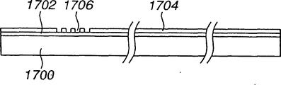
Secondly, the method for making of the two-dimentional optical guided wave device of present embodiment is described.Figure 10 is the schematic cross sectional view of this manufacture method of explanation.In the figure, the 1700th, glass substrate, the 1702nd, electroplate and use comprehensive electrode, the 1704th, photoresist, the 1706th, electroplate and use window, the 1708th, the divergent structure body, 1710 is the 2nd light chopper structures, 1712 is the 1st light chopper structures, the 1714th, and core layer, 1716 is the 2nd coverings, the 1718th, electrode wiring, the 1720th, semiconductor laser, the 1722nd, photo detector, 1724 is the 1st coverings.
The method for making of the two-dimentional optical guided wave device of present embodiment is also roughly similarly carried out with the method for making of Fig. 3 of embodiment 1.Difference is following operation: as shown in Figure 10 D, use the mould that utilizes Si (111) face to form to form the 1st light chopper structure 1712 of quadrangle cone shape, this structure is configured in plating with on comprehensive electrode 1702.
Making up the photoelectricity fusion substrate that above-mentioned two-dimentional optical guided wave device and circuit substrate are made shown in Figure 11 A.Near light signal injection part shown in Figure 11 B.In Figure 11, the 1800th, CPU, 1802 and 1804 is RAM, the 1806th, other electron device, the 1808th, transmission lines, the 1810th, light-emitting component, the 1812nd, photo detector, the 1814th, divergent structure body, the 1816th, light beam, the 1818th, the light that has been scattered, 1820 is the 1st light chopper structures.
In the present embodiment, also similarly to Example 1, can reduce in existing signal wire wiring itself significantly becomes antenna and has produced the Electromagnetic Launching noise that the circuit that causes because of the sharing model noise radiation delays work, and can improve EMI.In addition, and compare with the situation that two-dimensional approach is dispersed light signal to transmit from beginning at first,, can suppress the loss of luminous power by in the zone of transmitting, needing signal in the zone of transmitting with light beam light being dispersed at undesired signal.
(embodiment 6)
Figure 12 A shows the two-dimentional optical guided wave device of the embodiment 6 of the structure that 4 quadrangular pyramid sides of 4 light beams that light-emitting component and the 1st light chopper structure are configured to penetrate from the surface luminous semiconductor laser array element with 4 exits wound of bullet and the 1st light chopper structure of quadrangular pyramid type are coupled.And Figure 12 B shows the enlarged drawing of the position relation of light-emitting component and the 1st light chopper structure.In Figure 12,1900 is the 1st coverings, the 1902nd, and core layer, 1904 is the 2nd coverings, 1906 is the 1st light chopper structures, the 1908th, the divergent structure body, 1910 is the 2nd light chopper structures, the 1912nd, light-emitting component, and also 1914 are photo detectors.
As shown in Figure 12, by making identical signal from propagating from the beginning of becoming 4 light beams, and make 1 light beam be divided into the situation that 4 light beams propagate to compare, can suppress the loss of luminous power, carry out light efficiently and transmit.By being coupled with divergent structure body 1908 as required, make 4 light beams in two-dimentional optical guided wave device, propagating on the directions of 360 degree, disperse or on the part direction, disperse.Original state that also can use catoptron to press light beam changes the direction of propagation.
In addition, become the 2nd light chopper structure 1910 of polygonal wimble structure, also can make with the light of the inclined-plane coupling of polygonal wimble structure body crookedly upward, accept light signal with the photo detector that is configured to array-like by use.
In the present embodiment, used surface luminous semiconductor laser, but the number of exit wound of bullet is not limited to this with 4 exits wound of bullet, can be identical or lack than it with the number on the inclined-plane of the 1st light chopper structure that becomes polygonal wimble structure.In addition, in the present embodiment, having used the quadrangular pyramid type as the 1st light chopper structure, but be not limited to this, also can be wedge structure or polygonal wimble structure.In addition, also be same about the 2nd light chopper structure 1910.Not necessarily need the 2nd light chopper structure.
Configuration is played under the situation of structure of mirror function in the light wiring layer, can make that the light beam of propagating is in statu quo crooked to carry out the transmission of light signal with the barrier of avoiding the path etc. in the light wiring layer.
(embodiment 7)
Figure 13 show the surface of two-dimentional light-guide wave path or internal configurations formed the two-dimentional optical guided wave device of embodiment 7 of the globe-type luminescence component structure of electron device from the teeth outwards.In Figure 13,2000 is the 1st coverings, the 2002nd, and core layer, 2004 is the 2nd coverings, the 2006th, divergent structure body, the 2008th, light chopper structure, the 2010th, globe-type luminescence element, the 2012nd, photo detector.In addition, Figure 15 has shown in the internal configurations of two-dimentional light-guide wave path the similar two-dimentional light-guide wave path of the structure of the globe-type luminescence element that formed electron device from the teeth outwards and spherical photo detector.In Figure 15,2200 is the 1st coverings, the 2202nd, and core layer, 2204 is the 2nd coverings, the 2206th, divergent structure body, the 2208th, globe-type luminescence element, the 2210th, spherical photo detector.By by this way the photo detector 2210 of sphere being imbedded in the two-dimentional optical waveguide layer,, also can accept the light signal that sends efficiently even do not use light chopper structure etc.
Figure 14 shows the skeleton diagram of globe-type luminescence element and spherical photo detector.In Figure 14, the 2100th, light-emitting component, the 2102nd, electron device, the 2104th, electrical wiring, the 2106th, the n layer of spherical photo detector, the 2108th, i layer, the 2110th, p layer, the 2112nd, photo detector electrode.
As shown in Figure 14 A, propagate by making identical signal become 4 light beams from 4 light-emitting components 2100 that form at spherical device, with make 1 light beam be divided into the situation that 4 light beams propagate to compare, can suppress the loss of luminous power, carry out light efficiently and transmit.The electron device 2102 that forms on this sphere device is the cmos circuits that are used for driven light-emitting element 2100.
In the present embodiment, 4 light-emitting components 2100 are surface-emitting lasers of the GaInNAs/AlGaAs series that forms on 4 (111) faces, but are not limited to this, also can be β-FeSi
2Series etc.In addition, in the present embodiment, the electron device 2102 that forms on the surface of spherical device is light emitting element driving circuits, but is not limited to this, also can be integrated device of parallel/serial translation circuit, driving circuit and parallel/serial translation circuit etc.Perhaps, also can form a plurality of electron devices.
In the photo detector of sphere, form the pin layer on the surface of spherical Si substrate (for example the Southern Hemisphere one side), in addition, on the hemisphere (for example Northern Hemisphere) of an opposite side, formed light accepting part has been applied (not shown) such as circuit that reverse bias uses or amplifying circuits with light accepting part.
By making 4 light beams and 2006,2206 couplings of divergent structure body of in two-dimentional optical guided wave device, propagating as required, make it on the directions of 360 degree, disperse or on the part direction, disperse.
In addition, in the present embodiment, show two-dimentional optical guided wave device, but also can merge substrate with the incompatible making photoelectricity of circuit substrate group similarly to Example 2.Dispose under the situation of the structure that plays mirror function in the light wiring layer, the light beam bending that propagation is come is carried out the transmission of light signal with the barriers of avoiding in the light wiring layer such as path.
(embodiment 8)
Figure 16 shows the sectional view of the photoelectricity fusion substrate of the embodiment 8 with 2 light wiring layers that connect through the light through hole, in Figure 16, the 2900th, CPU, the 2902nd, RAM, the 2904th, light-emitting component, the 2906th, photo detector, the 2908th, path, the 2910th, electrical wiring layer, the 2912nd, the light wiring layer, the 2914th, electron device, the 2916th, the light chopper structure, and also 2918 are light through holes.
As shown in Figure 16, by connecting the light wiring layer each other, can make with the lightray propagation of some smooth wiring layer couplings and arrive other a plurality of smooth wiring layers with light through hole 2918.By connecting a plurality of smooth wiring layers 2912 by this way each other, can more transmit light signal efficiently in the wide region.
In Figure 16,, can on the direction vertical, transmit light beam with light wiring layer 2912 by the light chopper of the configuration up and down structure 2916 (for example being the small diffusing structure body of circular cone or polygonal cone-shaped) of the light through hole 2918 that extends in vertical direction.In the present embodiment, use light chopper structure 2916 on the direction vertical, to transmit light beam, but also can use catoptron to replace light chopper structure 2916 to transmit in vertical direction with light wiring layer 2912.
In addition, in the present embodiment, show situation about propagating as light beam by original state change direction of propagation of light beam towards photo detector 2906 from light-emitting component 2904, but be not limited to this, for example, be coupled towards top light wiring layer light beam of propagating and the divergent structure body that in the light wiring layer of top, disposes by making, also can make it on the directions of 360 degree, disperse or on the part direction, disperse from bottom light wiring layer.
In the present embodiment, at the inner filling of light through hole 2918 material same with the core material layer of two-dimentional optical waveguide layer, but be not limited to this.It also can be compaction material and become air structure or go into the structure of optical fiber or lens in light through hole 2918 interpolations not in light through hole 2918.
(embodiment 9)
Figure 17 shows the sectional view of the photoelectricity fusion substrate of the embodiment 9 with 2 light wiring layers that connect through the light through hole.In Figure 17, the 4000th, CPU, the 4002nd, RAM, the 4004th, light-emitting component, the 4006th, photo detector, the 4008th, path, the 4010th, electrical wiring layer, the 4012nd, light wiring layer, the 4014th, electron device, the 4016th, light chopper structure, the 4018th, divergent structure body, the 4020th, light through hole.
Similarly to Example 8, by connecting light wiring layer 4012 each other, make with the lightray propagation of some smooth wiring layer couplings and arrive other a plurality of smooth wiring layers with light through hole 4020.
In the present embodiment, as shown in Figure 17, directly over light through hole 4020, disposed divergent structure body 4018, be coupled, made it on the directions of 360 degree, disperse or on the part direction, disperse by propagate the light beam and the divergent structure body 4018 that come from the downside of light through hole 4020.In the present embodiment, in the inside of light through hole 4020 also filling the material same with the core material layer of two-dimentional optical waveguide layer, but be not limited to this.
(embodiment 10)
Figure 18 shows the sectional view of the photoelectricity fusion substrate of the embodiment 10 with 2 light wiring layers that connect through the light through hole.In Figure 18, the 4100th, CPU, the 4102nd, RAM, the 4104th, globe-type luminescence element, the 4106th, photo detector, the 4108th, path, the 4110th, electrical wiring layer, the 4112nd, light wiring layer, the 4114th, electron device, the 4116th, divergent structure body, the 4118th, light through hole.
Similarly to Example 8, by connecting light wiring layer 4112 each other, make with the lightray propagation of some smooth wiring layer couplings and arrive other a plurality of smooth wiring layers with light through hole 4118.
In the present embodiment, as shown in Figure 18, under light through hole 4118, disposed globe-type luminescence element 4104,2 light beams from 3 light beams that globe-type luminescence element 4104 penetrates are propagated in the light wiring layer of bottom, made 1 remaining light beam propagate into top light wiring layer by light through hole 4118.By using globe-type luminescence element 4104 by this way, and use the light chopper structure that light beam is propagated with the situation that signal is sent to a plurality of smooth wiring layers in the light through hole to compare, can suppress the loss of luminous power, make its transmission efficiently.
In the present embodiment, disposed divergent structure body 4116 directly over light through hole 4118, but be not limited to this, also configurable light chopper structure or catoptron etc. make light beam and the coupling of top light wiring layer.In the present embodiment, in the inside of light through hole 4118 also filling the material same with the core material layer of two-dimentional optical waveguide layer, but be not limited to this.
Claims (12)
1. an optical guided wave device possesses light sends the sending part of light and is received in the light of propagating in this guided wave road at the sheet light-guide wave path of propagating on the two-dimensional directional, in this guided wave road receiving portion, it is characterized in that:
Possessing the relay that the light that sends from this sending part and propagate is carried out relaying and sends this receiving portion between this sending part and the receiving portion in this guided wave road,
Wherein, above-mentioned relay comprises the light divergent structure body that is made of a plurality of protrusions in the above-mentioned guided wave road.
2. the optical guided wave device described in claim 1 is characterized in that:
The spread state of the light that above-mentioned relay is propagated in the plane on above-mentioned guided wave road with the trunking scheme change on transmitter side and the path accepting to propagate between the side.
3. the optical guided wave device described in claim 1 is characterized in that:
Above-mentioned relay comprises makes the structure of dispersing or dispersing with the light beam of light beam state propagation on the part direction on whole directions of 360 degree in the plane on above-mentioned guided wave road.
4. the optical guided wave device described in claim 3 is characterized in that:
The thickness of said structure body is less than the thickness of the core layer of above-mentioned guided wave road floor.
5. the optical guided wave device described in claim 1 is characterized in that:
Above-mentioned relay comprises change with the light beam of the light beam state propagation reflective structure body by the direction of the original state propagation of light beam.
6. the optical guided wave device described in claim 1 is characterized in that:
Above-mentioned relay be do not amplify or the situation of the Regeneration Treatment of shaping under change the structure of the spread state of the light of being propagated.
7. the optical guided wave device described in claim 1 is characterized in that:
The structure that above-mentioned guided wave road floor has had the sheet core layer stacked and clamped the 1st and the 2nd covering of this core layer.
8. the optical guided wave device described in claim 1 is characterized in that:
The light-emitting component of transmitter side is configured in the surperficial and even inner of above-mentioned guided wave road with at least one side who accepts the photo detector of side.
9. the optical guided wave device described in claim 8 is characterized in that:
Disposed in the guided wave road part under this light-emitting component and made the optical beam transformation more than 1 or 1 that sends from above-mentioned light-emitting component light chopper structure for the light beam propagated towards the prescribed direction more than 1 or 1.
10. the optical guided wave device described in claim 9 is characterized in that:
Above-mentioned light chopper structure is the structure of sphere, semisphere, taper shape, wedge shape or polygonal taper.
11. the optical guided wave device described in claim 10 is characterized in that:
Above-mentioned light-emitting component is to be configured to make monomer or the array-like surface-emitting laser that sends on the inclined-plane that couples light to above-mentioned light chopper structure.
12. one kind has merged the photoelectricity that light signal transmits and electronic signal transmits and has merged circuit board, possess light-guide wave path device and the electrical wiring layer that is electrically connected on this light-guide wave path device, above-mentioned light-guide wave path device has light sends the sending part of light and is received in the light of propagating in this guided wave road at the sheet light-guide wave path of propagating on the two-dimensional directional, in this guided wave road receiving portion, it is characterized in that:
This optical guided wave device is also possessing the relay that the light that sends from this sending part and propagate is carried out relaying and sends this receiving portion in this guided wave road between this sending part and the receiving portion, by using this optical guided wave device to send and accept light signal, partly or entirely connecting up of this electrical wiring layer signal made electronic device works
Wherein, above-mentioned relay comprises the light divergent structure body that is made of a plurality of protrusions in the above-mentioned guided wave road.
Applications Claiming Priority (2)
| Application Number | Priority Date | Filing Date | Title |
|---|---|---|---|
| JP219251/2002 | 2002-07-29 | ||
| JP2002219251A JP2004061799A (en) | 2002-07-29 | 2002-07-29 | Two-dimensional waveguide apparatus and opto-electronic fusion wiring board using same |
Publications (2)
| Publication Number | Publication Date |
|---|---|
| CN1475824A CN1475824A (en) | 2004-02-18 |
| CN1220078C true CN1220078C (en) | 2005-09-21 |
Family
ID=30112894
Family Applications (1)
| Application Number | Title | Priority Date | Filing Date |
|---|---|---|---|
| CN03152348.XA Expired - Fee Related CN1220078C (en) | 2002-07-29 | 2003-07-29 | 2-D optical waveguide device and photoelectric fuse wiring substrate using same |
Country Status (4)
| Country | Link |
|---|---|
| US (1) | US7120325B1 (en) |
| EP (1) | EP1387193A1 (en) |
| JP (1) | JP2004061799A (en) |
| CN (1) | CN1220078C (en) |
Families Citing this family (17)
| Publication number | Priority date | Publication date | Assignee | Title |
|---|---|---|---|---|
| KR20050004005A (en) * | 2003-07-01 | 2005-01-12 | 마츠시타 덴끼 산교 가부시키가이샤 | Mount assembly, optical transmission line and photoelectric circuit board |
| FI20035223A (en) * | 2003-11-27 | 2005-05-28 | Asperation Oy | Circuit boards and procedure for its manufacture |
| JP4789423B2 (en) * | 2004-03-30 | 2011-10-12 | キヤノン株式会社 | Optical waveguide device |
| US7483466B2 (en) * | 2005-04-28 | 2009-01-27 | Canon Kabushiki Kaisha | Vertical cavity surface emitting laser device |
| AT503585B1 (en) * | 2006-05-08 | 2007-11-15 | Austria Tech & System Tech | PCB ELEMENT ELEMENT AND METHOD FOR THE PRODUCTION THEREOF |
| AT503027B1 (en) | 2006-05-08 | 2007-07-15 | Austria Tech & System Tech | Printed circuit board element for multi-mode or single mode waveguide data transmission, has opto-electronic component embedded in optical photo-polymerizable layered material, and component has curved deviation mirror |
| TW200807047A (en) * | 2006-05-30 | 2008-02-01 | Sumitomo Bakelite Co | Substrate for mounting photonic device, optical circuit substrate, and photonic device mounting substrate |
| JP2008158440A (en) * | 2006-12-26 | 2008-07-10 | Toshiba Corp | Photoelectric wiring board and method of manufacturing photoelectric wiring apparatus |
| JP5020866B2 (en) * | 2007-05-07 | 2012-09-05 | キヤノン株式会社 | Vertical cavity surface emitting laser |
| WO2008149734A1 (en) * | 2007-05-31 | 2008-12-11 | Sony Corporation | Optical waveguide, signal processing device, and signal processing substrate |
| JP5370714B2 (en) | 2007-05-31 | 2013-12-18 | ソニー株式会社 | Optical waveguide and signal processing apparatus |
| US7912328B2 (en) * | 2008-11-26 | 2011-03-22 | General Electric Company | Optical waveguide EMI shield |
| DE102009051188A1 (en) * | 2009-10-29 | 2011-05-19 | Siemens Aktiengesellschaft | Light signal transmitter and light receiver for an optical sensor |
| WO2012043417A1 (en) * | 2010-10-01 | 2012-04-05 | 住友ベークライト株式会社 | Optical waveguide module, method for producing optical waveguide module, and electronic apparatus |
| US9204551B2 (en) | 2010-11-22 | 2015-12-01 | Lenovo Innovations Limited (Hong Kong) | Mounting structure and mounting method |
| US9377596B2 (en) * | 2014-07-22 | 2016-06-28 | Unimicron Technology Corp. | Optical-electro circuit board, optical component and manufacturing method thereof |
| TWI591834B (en) | 2014-08-12 | 2017-07-11 | Pgi股份有限公司 | Optical sensor and manufacturing method thereof |
Family Cites Families (14)
| Publication number | Priority date | Publication date | Assignee | Title |
|---|---|---|---|---|
| US4611883A (en) | 1981-05-01 | 1986-09-16 | Hughes Aircraft Company | Two-dimensional optics element for correcting aberrations |
| US4838630A (en) | 1987-12-21 | 1989-06-13 | Physical Optics Corporation | Holographic planar optical interconnect |
| US5198008A (en) | 1990-11-09 | 1993-03-30 | National Semiconductor Corporation | Method of fabricating an optical interconnect structure |
| RU2097815C1 (en) * | 1993-02-12 | 1997-11-27 | Фирма "Самсунг Электроникс Ко., Лтд." | Optical processor |
| JPH0996746A (en) | 1995-09-29 | 1997-04-08 | Fujitsu Ltd | Active optical circuit sheet or active optical circuit board |
| US5835646A (en) | 1995-09-19 | 1998-11-10 | Fujitsu Limited | Active optical circuit sheet or active optical circuit board, active optical connector and optical MCM, process for fabricating optical waveguide, and devices obtained thereby |
| US5822475A (en) * | 1995-12-20 | 1998-10-13 | Fuji Xerox Co., Ltd. | Optical bus and signal processor |
| JP2000199827A (en) | 1998-10-27 | 2000-07-18 | Sony Corp | Optical wave guide device and its manufacture |
| JP3728147B2 (en) * | 1999-07-16 | 2005-12-21 | キヤノン株式会社 | Opto-electric hybrid wiring board |
| US7020400B2 (en) | 1999-12-24 | 2006-03-28 | Altera Corporation | Multi-wavelength optical communication system |
| US6661940B2 (en) * | 2000-07-21 | 2003-12-09 | Finisar Corporation | Apparatus and method for rebroadcasting signals in an optical backplane bus system |
| JP3762208B2 (en) * | 2000-09-29 | 2006-04-05 | 株式会社東芝 | Optical wiring board manufacturing method |
| TW499581B (en) * | 2001-06-29 | 2002-08-21 | Ind Tech Res Inst | Planar waveguide diffractive beam splitter/beam coupler |
| JP2004013113A (en) * | 2002-06-11 | 2004-01-15 | Sumitomo Electric Ind Ltd | Optical signal processor |
-
2002
- 2002-07-29 JP JP2002219251A patent/JP2004061799A/en not_active Withdrawn
-
2003
- 2003-07-25 US US10/626,535 patent/US7120325B1/en not_active Expired - Fee Related
- 2003-07-28 EP EP03017112A patent/EP1387193A1/en not_active Withdrawn
- 2003-07-29 CN CN03152348.XA patent/CN1220078C/en not_active Expired - Fee Related
Also Published As
| Publication number | Publication date |
|---|---|
| JP2004061799A (en) | 2004-02-26 |
| EP1387193A1 (en) | 2004-02-04 |
| US7120325B1 (en) | 2006-10-10 |
| CN1475824A (en) | 2004-02-18 |
Similar Documents
| Publication | Publication Date | Title |
|---|---|---|
| CN1220078C (en) | 2-D optical waveguide device and photoelectric fuse wiring substrate using same | |
| JP3848210B2 (en) | Electronic circuit board | |
| US20200403107A1 (en) | Light emitting structure | |
| CN1211954C (en) | Receiving equipment, transmitting equipment and communication system | |
| CN2697670Y (en) | Optics element and device | |
| CN1802579A (en) | Three-dimensional photonic crystal waveguide structure | |
| CN1993639A (en) | Photoelectric integrated circuit element and transmission apparatus using the same | |
| JP4690870B2 (en) | Opto-electric integrated wiring board and opto-electric integrated wiring system | |
| CN1601313A (en) | Apparatus and methods for integrally packaging optoelectronic devices, IC chips and optical transmission lines | |
| CN1139984A (en) | Interconnection optical a fibre parallel | |
| CN100359830C (en) | Bidirectional optical transmission apparatus | |
| TW200630655A (en) | Photo-electricity combined-circuit mounted board and transmitting apparatus using the same | |
| CN1402030A (en) | Optic element, optic waveguide device, mfg. method thereof and light and electric hybrid carried base board | |
| CN101876732B (en) | Transmitting terminal module and receiving terminal module with optical waveguide structures | |
| CN1416533A (en) | Improved integrated optical device | |
| CN1735828A (en) | Photonic circuit board | |
| CN101206282A (en) | Optical circuit board | |
| JP2003279770A (en) | Optical transmission sheet, photoelectric fusion substrate using the same, and optical transmission method | |
| US20240012215A1 (en) | Coupling microleds to optical communication channels | |
| JP2005062557A (en) | Optical element device, two-dimensional optical waveguide element using the same and optoelectronic fusion wiring substrate | |
| CN104040397B (en) | For combination underfill barricade and the electric interconnection structure of photoelectricity engine | |
| CN106980160B (en) | On piece light-source structure based on hybrid integrated and preparation method thereof | |
| JP2003131081A (en) | Semiconductor device, photoelectric combined substrate, method for manufacturing the same, and electronics device using the same | |
| TWI393509B (en) | Optoelectric hybrid circuit board and manufacture thereof | |
| CN203480083U (en) | Optical interface device |
Legal Events
| Date | Code | Title | Description |
|---|---|---|---|
| C06 | Publication | ||
| PB01 | Publication | ||
| C10 | Entry into substantive examination | ||
| SE01 | Entry into force of request for substantive examination | ||
| C14 | Grant of patent or utility model | ||
| GR01 | Patent grant | ||
| CF01 | Termination of patent right due to non-payment of annual fee |
Granted publication date: 20050921 Termination date: 20140729 |
|
| EXPY | Termination of patent right or utility model |