CN1198428C - Modulation technique for transmitting a high data rate signal and an auxiliary data signal through a band limited channel - Google Patents
Modulation technique for transmitting a high data rate signal and an auxiliary data signal through a band limited channel Download PDFInfo
- Publication number
- CN1198428C CN1198428C CNB018161871A CN01816187A CN1198428C CN 1198428 C CN1198428 C CN 1198428C CN B018161871 A CNB018161871 A CN B018161871A CN 01816187 A CN01816187 A CN 01816187A CN 1198428 C CN1198428 C CN 1198428C
- Authority
- CN
- China
- Prior art keywords
- signal
- carrier
- pulse
- data signal
- interval
- Prior art date
- Legal status (The legal status is an assumption and is not a legal conclusion. Google has not performed a legal analysis and makes no representation as to the accuracy of the status listed.)
- Expired - Fee Related
Links
- 238000000034 method Methods 0.000 title claims description 12
- 230000007704 transition Effects 0.000 description 19
- 238000010586 diagram Methods 0.000 description 15
- 230000005236 sound signal Effects 0.000 description 11
- 238000005516 engineering process Methods 0.000 description 10
- 239000002131 composite material Substances 0.000 description 7
- 230000003321 amplification Effects 0.000 description 4
- 230000006835 compression Effects 0.000 description 4
- 238000007906 compression Methods 0.000 description 4
- 238000003199 nucleic acid amplification method Methods 0.000 description 4
- 230000005540 biological transmission Effects 0.000 description 3
- 238000001914 filtration Methods 0.000 description 3
- 238000012546 transfer Methods 0.000 description 3
- 230000010363 phase shift Effects 0.000 description 2
- 238000012545 processing Methods 0.000 description 2
- 238000011084 recovery Methods 0.000 description 2
- 238000007493 shaping process Methods 0.000 description 2
- 241001161843 Chandra Species 0.000 description 1
- 241001269238 Data Species 0.000 description 1
- 230000018199 S phase Effects 0.000 description 1
- 230000003139 buffering effect Effects 0.000 description 1
- 238000006243 chemical reaction Methods 0.000 description 1
- 150000001875 compounds Chemical class 0.000 description 1
- 238000012937 correction Methods 0.000 description 1
- 238000001514 detection method Methods 0.000 description 1
- 230000000694 effects Effects 0.000 description 1
- 238000004134 energy conservation Methods 0.000 description 1
- 239000000284 extract Substances 0.000 description 1
- 230000005764 inhibitory process Effects 0.000 description 1
- 238000012544 monitoring process Methods 0.000 description 1
- 230000035945 sensitivity Effects 0.000 description 1
- 238000001228 spectrum Methods 0.000 description 1
Images


Classifications
-
- H—ELECTRICITY
- H04—ELECTRIC COMMUNICATION TECHNIQUE
- H04L—TRANSMISSION OF DIGITAL INFORMATION, e.g. TELEGRAPHIC COMMUNICATION
- H04L5/00—Arrangements affording multiple use of the transmission path
- H04L5/02—Channels characterised by the type of signal
-
- H—ELECTRICITY
- H04—ELECTRIC COMMUNICATION TECHNIQUE
- H04L—TRANSMISSION OF DIGITAL INFORMATION, e.g. TELEGRAPHIC COMMUNICATION
- H04L27/00—Modulated-carrier systems
-
- H—ELECTRICITY
- H04—ELECTRIC COMMUNICATION TECHNIQUE
- H04L—TRANSMISSION OF DIGITAL INFORMATION, e.g. TELEGRAPHIC COMMUNICATION
- H04L25/00—Baseband systems
- H04L25/38—Synchronous or start-stop systems, e.g. for Baudot code
- H04L25/40—Transmitting circuits; Receiving circuits
- H04L25/49—Transmitting circuits; Receiving circuits using code conversion at the transmitter; using predistortion; using insertion of idle bits for obtaining a desired frequency spectrum; using three or more amplitude levels ; Baseband coding techniques specific to data transmission systems
- H04L25/4902—Pulse width modulation; Pulse position modulation
Landscapes
- Engineering & Computer Science (AREA)
- Signal Processing (AREA)
- Computer Networks & Wireless Communication (AREA)
- Physics & Mathematics (AREA)
- Spectroscopy & Molecular Physics (AREA)
- Digital Transmission Methods That Use Modulated Carrier Waves (AREA)
- Dc Digital Transmission (AREA)
Abstract
A digital data modulator (Fig. 8) is coupled to a source of a digital data signal having a data bit period, and a source of an auxiliary data signal. An encoder encodes the digital data using a variable pulse width code having edges occurring in an interval within the data bit period. A pulse signal generator, generates respective pulses representing the edges of the encoded digital data signal. A carrier signal generator generates a carrier signal having carrier pulses corresponding to the respective pulses during the interval, and modulated by the auxiliary data signal otherwise. A digital data demodulator (Fig. 9) is coupled to a source of a modulated signal including successive bit periods, each having a first interval containing a carrier pulse, spaced relative to other carrier pulses, to represent a variable pulse width encoded digital data signal, and a second interval during which the carrier is modulated with an auxiliary data signal. A detector demodulates the modulated signal to generate a variable pulse width encoded signal in response to received carrier pulses during the first interval, and an auxiliary data signal during the second interval. A decoder decodes the variable pulse width encoded signal to generate the digital data signal.
Description
Technical field
The present invention relates to a kind of modulation technique that high data rate signal and auxiliary data signal are provided by band limited channel.
Background technology
Always expecting provides data by having band-limited channel with High Data Rate.Many modulation techniques have been developed the data transfer rate that is used to improve by channel.For example, M unit's phase shift keying (PSK) and quadrature amplitude modulation (qam) technology allow the compression by a plurality of data bits of coding in the code element that is sent out at each.Such system has relative limitation.At first, relevant with these systems expensive hardware.This is because of the high-caliber channel linearity of these Technology Needs, so that suitably operation.Therefore, must carry out a large amount of signal processing to carrier track, symbol recovery, interpolation and signal shaping.The second, such technology is to the multipath effect sensitivity.The 3rd, these systems often require in some application (for example broadcasting FM subcarrier service on the in-band channel), can to obtain outside the data transfer rate of bandwidth to obtain to be expected.
Expectation is to provide several data-signals by a channel equally.Some modulation techniques are utilized channel fully, and some aspects of other remaining channels are not used.Frequency domain multiplexing and time-domain multiplexed are to be used for two kinds of technology that a plurality of signals are shared a channel.By shared channel by this way, improved whole throughput by channel.
Summary of the invention
According to principle of the present invention, a digital data modulator is connected to a digital data signal source and the auxiliary data signal source with data bit period.The variable pulse duration code with edge that occurs in the interval of encoder utilization in data bit period comes coding digital data.A pulse signal generator produces each pulse at the edge of the coded digital data signal of expression.A carrier signal generator produces carrier signal, and it has the carrier pulse corresponding to each pulse in the interval, otherwise is modulated by auxiliary data signal.
According to another aspect of the present invention, a digital data demodulator is connected to the modulating signal source that comprises continuous bit period, each bit period has: first at interval, comprise a carrier pulse alternate, to represent a variable pulse width coding digital data signal with other carrier pulses; Second at interval, utilizes an auxiliary data signal to come modulated carrier during this period.The signal that a detector demodulation is modulated with in response to first carrier pulse that receives at interval and second at interval auxiliary data signal and produce a variable pulse width coding digital data signal.A decoder decode variable pulse width coding digital data signal is to produce digital data signal.
The high data rate signal and the auxiliary signal that will send by single channel is provided according to the technology of principle of the present invention.Can utilize relatively cheap circuit to realize according to system of the present invention, multipath be disturbed insensitive, and provide the bandwidth reduction of essence.
According to modulates digital data method of the present invention, it is characterized in that comprising the following steps: to provide digital data signal with data bit period; The variable pulse width code with edge that occurs in the interval of utilization in data bit period comes the coding digital data signal; Each pulse at the edge of the digital data signal that the generation expression is encoded; An auxiliary data signal is provided; And producing a carrier signal, it has the carrier pulse corresponding with each pulse in described interval, is modulated by auxiliary data signal in other intervals.
According to digital data modulator of the present invention, it is characterized in that comprising: a digital data signal source with data bit period; An encoder (10) utilizes the variable pulse width code with edge that occurs in the interval in data bit period to come coding digital data; A pulse signal generator (20,25), each pulse that produces the edge of the coded digital data signal of expression; An auxiliary data signal source (AUX); A carrier signal generator (30,40) produces carrier signal, and it has the carrier pulse corresponding to each pulse in described interval, is modulated by auxiliary data signal in other intervals.According to digital data demodulator of the present invention, it is characterized in that comprising: a modulating signal source that comprises the successive bits cycle, each bit period has: comprise first interval of a carrier pulse alternate with other carrier pulses, be used to represent variable pulse width coding digital data signal; With second interval, come modulated carrier with an auxiliary data signal during this period; A detector (140) is used for signal that demodulation modulates producing the variable pulse width code signal in response to the carrier pulse that is received at interval first, produces an auxiliary data signal second at interval; A decoder (150), the described variable pulse width code signal that is used to decode is to produce digital data signal.
Description of drawings
In the accompanying drawings:
Fig. 1 is the block diagram that is used for being created in than the modulator of the higher data signal of narrow bandwidth;
Fig. 2 is the oscillogram that is used to understand the operation of modulator shown in Figure 1;
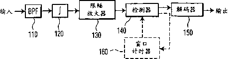
Fig. 3 is the block diagram of receiver that can receive the signal of modulation shown in Figure 1;
Fig. 4 is the spectrogram that is used to understand the modulation technique shown in Fig. 1 and 2;
Fig. 5 is the block diagram that comprises the FM broadcast transmitter of digital transmitting channel on the in-band channel that utilizes the modulation technology shown in Fig. 1 and 2;
Fig. 6 is the block diagram that can receive the FM broadcasting receiver of the signal of being modulated by FM broadcast transmitter shown in Figure 5;
Fig. 7 is the oscillogram that is used to understand according to the operation of the modulator of the principle of the invention;
Fig. 8 is the block diagram according to the modulator of principle of the present invention;
Fig. 9 is according to block diagram of the present invention, that can receive the receiver of the signal that is produced by modulator shown in Figure 8.
Embodiment
Fig. 1 is the block diagram that is used to produce the modulator of High Data Rate narrow band signal.In Fig. 1, input terminal IN receives a digital signal.This input IN is connected to the input of an encoder 10.The output of encoder 10 is connected to the input of a differentiator 20.The output of differentiator 20 is connected to the input of level detector 25.The output of level detector 25 is connected to the first input end of a frequency mixer 30.A local oscillator 40 is connected to second input of frequency mixer 30.The output of frequency mixer 30 is connected to the input of a band pass filter (BPF) 50.The output of BPF 50 is connected to an output OUT, and it produces the modulation signal of the digital signal that is illustrated in input IN.
Fig. 2 is the oscillogram that is used to understand the operation of modulator shown in Figure 1.Fig. 2 draws not in scale so that diagram waveform more clearly.In the graphic embodiment of institute, be the bi-level signal of non-return-to-zero (NRZ) form in the digital signal of input IN.This signal is illustrated in the upper waveform of Fig. 2.The NRZ signal has continuous bit, and each continues to be called as the predetermined period of bit period, is represented by the dotted line in the NRZ signal, and has the respective frequencies that is called as bit rate.The level of NRZ signal is represented the value of that bit, and this all is in known manner.Encoder 10 operation utilizes the variable pulse width NRZ signal of encoding.In an illustrated embodiment, the variable pulse width code is the variable aperture code.Describe variable aperture code on March 11st, 1999 in detail among International Patent Application PCT/US99/05301 that submit to, Chandra Mohan.In present patent application, phase code NRZ signal in the following manner.
Each bit period in the NRZ signal is encoded as a transition in code signal.The encoded clock of a M times more bits rate is used to phase code NRZ signal.In above-mentioned patent application, encoded clock is with the speed M operation of 9 times more bits rates.When the NRZ signal when logic ' 1 ' level transits to logic ' 0 ' level, 8 the encoded clock cycles (M-1) from previous transition in code signal are carried out transition.When the NRZ signal when logic ' 0 ' level transits to logic ' 1 ' level, 10 the encoded clock cycles (M+1) from previous transition in code signal are carried out transition.In the time of the not transition of NRZ signal, if promptly continuous bit has identical value, then 9 the encoded clock cycles (M) from last transition are carried out transition in code signal.Variable aperture code signal (VAC) is illustrated as second waveform in Fig. 2.
20 pairs of variable aperture code signals of differentiator (VAC) differential is to produce a succession of pulse consistent with transition time in the VAC signal.Differentiator also provides 90 degree phase shifts to the VAC modulation signal.The forward position transition produces the pulse of forward, and the back produces negative-going pulse along transition, and this all is in known manner.By the VAC signal of differential
In Fig. 2, be illustrated as the 3rd signal.25 pairs of level detectors
Signal carries out level detection to produce a succession of three level pulses with constant amplitude.When by the VAC signal of differential
When having the value greater than positive threshold value, produce level signal with high value; When it has value less than negative threshold value, produce a level signal, otherwise it has a median with low value, this all is in known manner.Level signal is shown as the 4th signal (LEVEL) in Fig. 2.
The LEVEL signal is modulated the carrier signal from local oscillator 40 in frequency mixer 30.Positive pulse produces the pulse of the carrier signal with first phase place, and negative pulse produces the pulse of the carrier signal with second phase place.The best phase place of first and second phase places differs roughly 180 degree.The carrier signal pulse preferably roughly an encoded clock cycle long, and have among the graphic embodiment duration of 1/9 of NRZ bit period roughly.The frequency of local oscillator 40 is selected so that preferably the local oscillator signal at least 10 cycles can take place during the cycle in carrier signal burst length.In Fig. 2, carrier signal CARR is illustrated as the pulse of bottom, wherein by representing carrier signal at the vertical shading of each rectangle envelope.In CARR signal shown in Figure 2, represent the phase place of the carrier pulse that produces in response to forward LEVEL pulse by "+", represent the phase place of the carrier pulse that produces in response to negative sense LEVEL pulse by "-"."+" and "-" only represents roughly differing of 180 degree, rather than will represent any absolute phase.
Fig. 3 is the block diagram of receiver that can receive the signal of the modulators modulate shown in Fig. 1 and 2.In Fig. 3, input IN is connected to as above the signal source with reference to the described modulation of Fig. 1 and 2.Input IN is connected to the input of BPF 110.The output of BPF 110 is connected to the input of an integrator 120.The output of integrator 120 is connected to the input of a limiting amplifier 130.The output of limiting amplifier 130 is connected to the input of a wave detector 140.The output of wave detector 140 is connected to the input of decoder 150.The output of decoder 150 reproduces by the NRZ signal of representing at the modulation signal of input IN, and is connected to output OUT.
Be in operation, BPF 110 filtered bands external signals are only by modulated SSB signal, as mentioned above.Integrator 120 will be by 90 degree phase shift paraphase of (Fig. 1's) differentiator 20 introducings.Limiting amplifier 130 will be restricted to constant amplitude from the amplitude of the signal of integrator 120.From the signal of limiting amplifier 130 corresponding to carrier pulse signal CARR shown in Figure 2.Wave detector 140 or a FM frequency discriminator, or a phase-locked loop (PLL) are used for the carrier pulse signal that difference demodulation FM or PM modulate.Wave detector 140 detected carrier pulses also produce a bi-level signal with transition of being represented by the phase place and the timing of those pulses.The output of wave detector 140 is and the corresponding variable bit width signal of VAC signal among Fig. 2.Decoder 150 carries out reverse operating to (Fig. 1's) encoder 10, and produces the NRZ signal corresponding with the NRZ signal of Fig. 2 at output OUT.Above-mentioned U.S. Patent application (RCA88,945) has illustrated the decoder 150 that can use in Fig. 3.Being utilized the circuit (not shown) subsequently at the NRZ of output OUT signal handles.
Because carrier pulse (the signal CARR of Fig. 2) occurs in the time that relative to each other defines, and because therefore the limited duration of those pulses might only allow wave detector 140 work when the needs pulse.For example, as above described in detail in the graphic embodiment of institute, each pulse has duration of 1/9 of time between the NRZ signal transition time roughly.After receiving a carrier pulse, only need consecutive pulses in 9/9 (no transition) or 10/9 (forward position) of time between the NRZ of that pulse signal transition from 8/9 of the time of previous carrier pulse (edge, expression back) between the NRZ signal transition.Similarly, after receiving a carrier pulse, only expect consecutive pulses in 8/9 (edge, back) or 9/9 (the no transition) of time between the NRZ of that pulse signal transition from 10/9 of the time of previous carrier pulse (expression forward position) between the NRZ signal transition.Only carrier pulse the time and only need allow wave detector 140 when expectation in the adjacent time of duration of the pulse of being expected.
Window timer shown in the frame of broken lines among Fig. 3 160 has the input of a state output end that is connected to wave detector 140 and the output of a permission input that is connected to wave detector 140.Window timer 160 monitoring is from the signal of wave detector 140, and only when expecting carrier pulse and only allows this wave detector in the adjacent time of duration of that pulse, as mentioned above.
In the graphic embodiment of institute, the energy in modulation signal mainly between 0.44 (8/18) times and 0.55 (10/18) times of bit rate, therefore has 0.11 times bandwidth of bit rate.This causes the data transfer rate by bandwidth has been improved 9 times.Can easily obtain other compression ratios by the ratio that changes encoded clock and bit rate, and have compromise and restriction that those skilled in the art understands easily.
Can in transmitter and receiver, use than M PSK of unit or the simpler circuit of QAM modulation technique and realize described system.Particularly, in receiver, after extracting modulated signal, can use limiting amplifier (as 130), it not only cheaply but also energy-conservation.And can utilize the quick programmable logic device of nominal (PLD) to carry out the Code And Decode of NRZ signal.Such device is cheap (present 1 to 2 dollar) comparatively.In addition, in this system, disturb between nonexistent code unit, therefore do not need waveform shaping.And, except the clock recovery loop, do not need tracking loop.
As mentioned above because the transmission of carrier wave only occurs over just bit boundaries (bit boundary) and do not continue for whole bit period, therefore can be in receiver window comes only needing the carrier pulse that time detecting received of pulse service time.Therefore, the problem that for native system, does not have multipath.
An application of above-mentioned modulation technique is the digital music that sends the CD quality with FM monophony and stereophonic broadcasting audio signal simultaneously.Fig. 4 is the spectrogram that is used to understand this application of the modulation technique shown in Fig. 1 and 2.Fig. 4 a illustrates the power envelope line that is used for the FM broadcast singal in the U.S..In Fig. 4 a, horizontal line is represented frequency, and is illustrated in the part of the VHF frequency band between about 88MHz and the about 107MHz.Represented signal strength signal intensity in vertical direction.Illustrate the permission envelope of the wave spectrum of two adjacent broadcast singals.Each carrier wave is illustrated as a vertical arrow.It around each carrier wave the sideband that has the broadcast singal of FM modulation on carrier wave.
In the U.S., FM radio station can be with total power broadcasting monophony and stereo audio in the sideband in the 100kHz carrier wave.In Fig. 4 a, these sidebands are illustrated by shadow-free ground.Other information can be broadcasted in the broadcasting station in the sideband from 100kHz to 200kHz, but the power that transmits in this frequency band must be than the low 30dB of total power.These sidebands are illustrated with shade.Adjacent broadcasting station (in the same geographic area) 400kHz at least of must being separated by.
The upper sideband on the carrier wave top of the low frequency broadcast singal in Fig. 4 a is illustrated in the spectrogram of Fig. 4 b.In Fig. 4 b, vertical direction is represented percent modulation.In Fig. 4 b, the modulation level with 90% in the 0-15kHz sideband sends monophonic audio signal L+R.Near repressed subcarrier frequency 38kHz, send L-R signal as the double-sideband suppressed-carrier signal with 45% modulation level.Lower sideband (lsb) is operated in from 23kHz to 38kHz, and upper sideband (usb) is operated in from 38kHz to 53kHz.The pilot tone (half of suppressed carrier frequency) that in the sideband of main carrier, also comprises a 19kHz.Therefore, the broadcasting station keeps the upper sideband (Fig. 4 b) and the 47kHz in the lower sideband (not shown) that can obtain near main carrier (promptly from 53kHz to 100kHz) to come with the other information of total power broadcasting.As mentioned above, the power that sends from 100kHz to 200kHz must be than the low 30dB of total power.
Utilize the modulation technique shown in aforesaid Fig. 1 and 2, can in less than the bandwidth of 20kHz, encode and send the signal of one 128 kilobits per second (kbps) that comprises MP3 CD quality audio signal.This digital audio and video signals can be arranged in 53kHz of (for example) upper sideband and the space between the 100kHz, and can be used as subcarrier signal and be sent out with the broadcasting stereo audio signal of rule, shown in Fig. 4 b.In Fig. 4 b, digital audio and video signals is the above-mentioned SSB signal of center at 70kHz, is operated in from about 60kHz to 80kHz.Therefore this signal can be sent out with total power in the 100kHz of main carrier.
Fig. 5 is the block diagram that comprises according to the FM broadcast transmitter of digital transmitting channel on the in-band channel of the described modulation technology of reference Fig. 1-3.In Fig. 5, in those identical elements shown in Figure 1 are enclosed in an empty frame that indicates " Fig. 1 ", and designated identical Reference numeral, do not describing in detail below.As described in reference Fig. 1 and 2, the SSB phase place or the frequency modulated signal (CARR of Fig. 2) of the combination results of encoder 10, differentiator 20, level detector 25, frequency mixer 30, oscillator 40 and BPF 50 expression digital input signals (NRZ among Fig. 2).The output of BPF 50 is connected to an output of amplifier 60.The output of amplifier 60 is connected to the first input end of second frequency mixer 70.Second oscillator 80 is connected to second input of second frequency mixer 70.An output of second frequency mixer 70 is connected to an input of first filter/amplifier 260.First filter/the output of amplifier 260 is connected to the first input end of signal combiner 250.
The output of broadcast baseband signal processor 210 is connected to the first input end of three-mixer 220.The 3rd oscillator 230 is connected to second input of three-mixer 220.The output of three-mixer 220 is connected to the input of second filter/amplifier 240.The output of second filter/amplifier 240 is connected to second input of signal combiner 250.The output of signal combiner is connected to the input of power amplifier 270, and power amplifier 270 is connected to transmitting antenna 280.
Be in operation, encoder 10 receives the digital signal of an expression digital audio and video signals.In a preferred embodiment, this signal is a MP3 compatible digital audio signal.Particularly, utilize Reed-Solomon (RS) sign indicating number to come forward error correction (FEC) coded digital audio data stream.With FEC coded data stream packets, these data that are grouped are become the SSB signal by circuit compression shown in Figure 1 then then, and are as above described in detail.
The frequency of the signal that is produced by oscillator 40 is selected as 10.7MHz, therefore near the centre frequency of 10.7MHz modulation from the digital information of encoder 10.Modulating frequency can be any frequency, but is selected to make its frequency corresponding to existing low-cost BPF filter more practically.For example, typical B PF filter has centre frequency 6MHz, 10.7MHz, 21.4MHz, 70MHz, 140MHz etc.In the graphic embodiment of institute, modulating frequency is selected as 10.7MHz, and BPF 50 is implemented as one of existing 10.7MHz filter.Be exaggerated that device 60 amplifies and by the combination up-conversion of second frequency mixer 70 and second oscillator 80 from the SSB signal of the filtering of BPF 50.In the graphic embodiment of institute, second oscillator 80 produces the signal of 77.57MHz, and SSB is up-converted to 88.27MHz.This signal is by first filter/amplifier 260 filtering and further amplification.
Broadcast baseband signal processor 210 receives a stereo audio signal (not shown), and execution forms the necessary signal processing of base band composite stereo acoustical signal, described base band composite stereo acoustical signal comprises the L+R signal of base band, in the double-sideband suppressed-carrier L-R signal of (inhibition) carrier frequency 38kHz and the pilot tone of 19kHz, this all is in known manner.This signal is modulated onto the carrier signal of the dividing frequency with FM broadcasting station subsequently.The 3rd oscillator 230 produce the 88.2MHz shown in having in the present embodiment distribute a carrier signal of base band frequency.Three-mixer 220 produces the modulated signals with compound monophony of the base band shown in Fig. 4 b and stereo audio signal modulation.Modulated signals with the standard broadcasting audio frequency sideband shown in 88.2MHz carrier frequency and Fig. 4 b is subsequently by second filter/amplifier 240 filtering and amplification.This signal and the modulated digital signal combination of the SSB that from the centre frequency of first filter/amplifier 260 is 88.27MHz are to form a composite signal.Therefore this composite signal is included in standard broadcasting stereo audio sideband of modulating on the 88.2MHz carrier wave and the SSB modulated signals that has the digital audio and video signals of the high 70kHz of center frequency ratio carrier wave (88.2MHz), shown in Fig. 4 b.This composite signal is subsequently by power amplifier 270 power amplifications, and is provided to transmitting antenna 280 to send to the FM wireless receiver.
Fig. 6 is the block diagram that can receive the FM broadcasting receiver of the signal of being modulated by FM broadcast transmitter shown in Figure 5.In Fig. 6, be enclosed in the dashed rectangle that indicates " Fig. 3 " with those identical elements shown in Figure 3, designated identical Reference numeral below does not describe in detail.In Fig. 6, a reception antenna 302 is connected to RF amplifier 304.The output of RF amplifier 304 is connected to the first input end of first frequency mixer 306.The output of first oscillator 308 is connected to second input of first frequency mixer 306.The output of first frequency mixer 306 is connected to each input of BPF 310 and tunable BPF 110.The output of BPF 310 is connected to an input of intermediate frequency (IF) amplifier 312, and intermediate frequency (IF) amplifier 312 can be a limiting amplifier.The output of IF amplifier 312 is connected to the input of FM detector 314.The output of FM detector 314 is connected to the input of FM stereodecoder 316.
Be in operation, 304 receptions of RF amplifier and amplification are from the RF signal of reception antenna 304.First oscillator 308 is created in the signal of 98.9MHz.The combination of first oscillator 308 and first frequency mixer 306 down-converts to 10.7MHz with the main carrier signal of 88.2MHz, and the SSB digital audio and video signals is down-converted to 10.63MHz from 88.27MHz.BPF 310 only passes through the FM stereophonic signal sideband (L+R and L-R) of 53kHz around 10.7MHz in known manner.IF amplifier 312 amplifies this signal, and it is provided to FM detector 314, and FM detector 314 produces base band composite stereo acoustical signal.The described base band composite stereo acoustical signal of FM stereodecoder 316 decoding is with the monophony and/or the stereo audio signal (not shown) of the audio signal that produces expression and sent, and this all is in known manner.
In the graphic embodiment of institute, tunable BPF 110 is tuned to centre frequency 10.63MHz, and only by 20kHz digital audio and video signals around that frequency.In the graphic embodiment of institute, the passband of BPF110 is operated in from 10.53MHz to 10.73MHz.The combination of BPF 110, integrator 120, limiting amplifier 130, wave detector 140, decoder 150 and window timer 160 moves in mode as described in Figure 3 and extracts modulated digital audio and video signals, and that signal of demodulation sign indicating number is to reproduce digital audio and video signals.Handle from the digital audio and video signals of decoder 150 to produce and the digital audio and video signals corresponding audio signal that is sent by suitable mode by another circuit (not shown).Particularly, the split grouping of signal, and detect and be corrected in any mistake of introducing during the transmission.The bit stream that is repaired is converted into stereo audio signal subsequently, and this all is in known manner.
The above embodiments provide the suitable compression performance with 1024 QAM systems.But in fact, the QAM system is limited to 256 QAM, because be difficult to correct because the noise and the multipath inter symbol interference that cause of constellation interval (constellationspacing) closely.Above-mentioned system does not have because the ISI problem of wide and narrow alternate carrier pulse.In brief, in narrow bandwidth channel, can send High Data Rate and not with such as the relevant problem of the other technologies of QAM.
Return referring to Fig. 2, in the CARR signal, between carrier pulse, have the gap of broad as can be seen, during this period, do not have carrier signal to be sent out.Can use these gaps according to the present invention.Fig. 7 is the more detailed oscillogram that is used to understand according to the CARR signal of the operation of modulator of the present invention.As mentioned above, in encoder shown in Figure 1 10, encoded clock signal has 1/9 one-period as the bit period of NRZ signal.Vertical dotted line presentation code clock signal period in Fig. 7.In Fig. 7, there are 9 clock cycle the bit period from time t1 to bit period of time t10 diagram to be illustrated in.But this bit period needn't be consistent in time with the NRZ input signal, probably with respect to NRZ signal delay.
The time location of the carrier pulse that is allowed is represented by dashed rectangle.A carrier pulse may occur in 8,9 or 10 clock pulse places of previous back.Therefore, carrier pulse can occur in any in three adjacent clock cycle.Suppose that carrier pulse A is from 8 previous clock pulse, suppose that carrier pulse B is from 9 previous clock pulse, suppose that carrier pulse C is from 10 previous clock pulse.
As mentioned above, when carrier pulse is 8 clock pulse from previous pulse (A), this is illustrated in the back edge in the NRZ signal, only can be immediately following being illustrated in unconverted one 9 clock pulse interval (D) in the NRZ signal or being illustrated in one 10 clock pulse interval (E) in the forward position in the NRZ signal.Similarly, when a carrier pulse is from previous pulse (C) 10 clock pulse the time, back edge in this expression NRZ signal, and be illustrated in one 8 clock pulse interval (E) in the forward position in the NRZ signal or be illustrated in unconverted one 9 clock pulse interval (F) in the NRZ signal to closely follow only.When a carrier pulse is 9 clock pulse from previous pulse (B), this is illustrated in no change in the NRZ signal, and can be immediately following one 8 clock pulse (D) on the back edge in the expression NPZ signal, be illustrated in unconverted one 9 clock pulse (E) in the NRZ signal or be illustrated in one 10 clock pulse interval (F) in the forward position in the NRZ signal.This all in Fig. 7 by diagram.Obviously, 9 encoded clock cycles in a NRZ bit period, promptly first of the described bit period that is made of one of three adjacent clock cycle (t1-t4) at interval, may comprise a carrier pulse, simultaneously, second interval that is made of other 6 clock cycle (t4-t10) can not have a carrier pulse.
The interim that in CARR signal (t4-t10), does not have carrier pulse to produce, can on carrier signal, modulate other auxiliary datas.This is illustrated as the round rectangle (AUXDATA) with vertical shading in Fig. 7.Keep each guard period Δ t; first last possible carrier pulse (C) in a bit period afterwards; second before the next possible continuously carrier pulse in the next bit period in this gap, so that carrying the carrier pulse of digital audio and video signals (A)-(F) and carrying possible minimum interference between the carrier modulation (AUX DATA) of auxiliary data.
Fig. 8 is the block diagram of one embodiment of the present of invention, and described embodiment can be implemented in the modulated encoded data stream and comprises auxiliary data.In Fig. 8, with graphic those the identical elements of Fig. 1 designated identical Reference numeral, and do not describe in detail below.In Fig. 8, an auxiliary data (AUX) source (not shown) is connected to the input of a first-in first-out (FIFO) buffer 402.The output of fifo buffer 402 is connected to first data input pin of multiplexer 404.The output of multiplexer 404 is connected to an input of frequency mixer 30.The output of level detector 25 is connected to second data input pin of multiplexer 404.A timing output of encoder 10 is connected to a control input end of multiplexer 404.
In the graphic embodiment of institute, suppose directly modulated carrier signal of auxiliary data signal.It will be appreciated by those skilled in the art that how to encode and/or prepare a signal in addition and come to come modulated carrier in the mode of the characteristic of suitable that signal.In addition, in the graphic embodiment of institute, suppose that auxiliary data signal is a digital form.But this not necessarily.Auxiliary data also can be an analog signal.
Be in operation, encoder 10 comprises internal timing circuit (not shown), is used for the relative timing of control impuls.This timing circuit can be modified to produce a signal in the mode that those skilled in the art understands, it has first state during three adjacent encoder clock cycle t1-t4 when pulse may occur in the CARR signal, it has second state during remaining encoded clock cycle t4-t10.This signal can be used to control multiplexer 404 the output of level detector 25 being connected to the input of frequency mixer 30 when may pulsing the time during Δ t1-Δ t4, and at Δ t4-Δ t10 the output of fifo buffer 402 is connected to frequency mixer 30 in addition.During the Δ t1-Δ t4 when the output when level detector 25 is connected to frequency mixer 30, the circuit of Fig. 8 is configuration as shown in Figure 1, and as above detailed described operation.
Be connected at fifo buffer 402 (considering boundary belt Δ t) during (t4+ Δ t is to the t10-Δ t) of frequency mixer 30, from the data-modulated of fifo buffer 402 carrier signal from oscillator 40.Fifo buffer 402 operations receive digital auxiliary data signal with the constant bit rate, and buffering signals during the time cycle (t1-t4) in the time can producing carrier pulse (A)-(C).Fifo buffer 402 provides the auxiliary data of being stored as burst with high bit rate to frequency mixer 30 at (t4+ Δ t is to the t10-Δ t) time durations in the time will sending auxiliary data subsequently.The net throughput of the burst of the auxiliary data by the CARR signal must mate the constant net throughput from the auxiliary data of auxiliary data signal source (not shown).It will be appreciated by those skilled in the art that how to mate throughput, and how to stipulate to exceed and underrun that this all is in known manner.
Fig. 9 is the block diagram that can receive the receiver of the signal that is produced by system shown in Figure 8.In Fig. 9, with those identical elements shown in Figure 3 designated identical Reference numeral, do not describe in detail below.In Fig. 9, the output of wave detector 140 is connected to the input of controllable switch 406.First output of controllable switch 406 is connected to the input of decoder 150.Second output of controllable switch 406 is connected to the input of FIFO 408.The output of FIFO 408 produces auxiliary data (AUX).The output of window timer 160 is not the permission output that is connected to wave detector 140, as shown in Figure 3, but replaces the control input end that is connected to controllable switch 406.
Be in operation, the wave detector 140 in Fig. 9 always is enabled.From the window signal of window timer 160 corresponding to the timing signal that in Fig. 8, produces by encoder 10.Window signal has first state during (t1-t4) when carrier pulse (A)-(C) may take place, at second state of other (t4-t10).During (t1-t4) when carrier pulse (A)-(C) may take place, window timer 160 makes controllable switch 406 that wave detector 140 is connected to decoder 150.This configuration is with shown in Figure 3 identical, and as above detailed described such operation.
In the remaining time of bit period (t4-t10).Wave detector 140 is connected to FIFO 408.During this period, the auxiliary data of being modulated is separated to be in harmonious proportion and is provided to FIFO 408.Utilize the mode corresponding with (Fig. 8's) FIFO 402, FIFO 408 receives the auxiliary data pulse trains from wave detector 140, and with constant bit rate generation auxiliary data output signal AUX.Auxiliary data signal is represented the coded auxiliary data that is used for modulated carrier.May need further to handle (not shown) the auxiliary data signal that is received is decoded as the form of being expected.
Claims (19)
1, a kind of modulates digital data method is characterized in that comprising the following steps:
Digital data signal with data bit period is provided;
The variable pulse width code with edge that occurs in the interval of utilization in data bit period comes the coding digital data signal;
Each pulse at the edge of the digital data signal that the generation expression is encoded;
An auxiliary data signal is provided; And
Produce a carrier signal, it has the carrier pulse corresponding with each pulse in described interval, is modulated by auxiliary data signal in other intervals.
2. according to the modulator approach of claim 1, it is characterized in that described code is a variable aperture code.
3. digital data modulator is characterized in that comprising:
Digital data signal source with data bit period;
An encoder (10) utilizes the variable pulse width code with edge that occurs in the interval in data bit period to come coding digital data;
A pulse signal generator (20,25), each pulse that produces the edge of the coded digital data signal of expression;
An auxiliary data signal source (AUX);
A carrier signal generator (30,40) produces carrier signal, and it has the carrier pulse corresponding to each pulse in described interval, is modulated by auxiliary data signal in other intervals.
4. according to the modulator of claim 3, it is characterized in that, described modulator also comprises: a multiplexer (404), has the pulse signal generator of being connected to (20,25) first data input pin, second data input pin, be connected to auxiliary data signal source (AUX), with an output that connects with carrier signal generator (30,40), and be adjusted make first at interval in pulse signal generator (20,25) be connected to carrier signal generator (30,40), in other intervals, auxiliary data signal source (AUX) is connected to carrier signal generator (30,40).
5. according to the modulator of claim 4, it is characterized in that also being included in a first-in first-out fifo buffer (402) that connects between auxiliary data source and the multiplexer (404).
6. according to the modulator of claim 3, it is characterized in that the variable pulse width code is a variable aperture code.
7. according to the modulator of claim 3, it is characterized in that:
Encoder (10) produces the coding digital data signal with forward position and edge, back;
Pulse signal generator (20,25) produces positive pulse in response to the forward position in digital data signal, and produces negative pulse in response to the back edge in this digital data signal;
Carrier signal generator (30,40) produces a carrier pulse, and it has in response to first phase place of positive pulse with in response to second phase place of negative pulse.
8. according to the modulator of claim 7, it is characterized in that first phase place and second phasic difference 180 degree mutually.
9. according to the modulator of claim 3, it is characterized in that described pulse signal generator comprises:
A differentiator (20) is connected to encoder;
A level detector (25) is connected to differentiator.
10. according to the modulator of claim 3, it is characterized in that carrier signal generator comprises:
A carrier oscillator (40); With
A frequency mixer (30) has the first input end of the pulse signal generator of being connected to (20,25) and is connected to second input of carrier oscillator (40).
11. according to the modulator of claim 10, its feature also is also to comprise a band pass filter (50) that is connected to the output of frequency mixer (30).
12. a digital data demodulator is characterized in that comprising:
A modulating signal source that comprises the successive bits cycle, each bit period has: comprise first interval of a carrier pulse alternate with other carrier pulses, be used to represent variable pulse width coding digital data signal; With second interval, come modulated carrier with an auxiliary data signal during this period;
A detector (140) is used for signal that demodulation modulates producing the variable pulse width code signal in response to the carrier pulse that is received at interval first, produces an auxiliary data signal second at interval;
A decoder (150), the described variable pulse width code signal that is used to decode is to produce digital data signal.
13. demodulator according to claim 12, it is characterized in that also comprising: a gate-controlled switch (406), has the input that is connected to detector (140), first output, be connected to decoder (150), and second output, described demodulator also is adjusted and makes and produce the variable pulse width code signal at first output, produces auxiliary data signal at second output.
14. according to the demodulator of claim 13, its feature also is also to comprise a fifo buffer (408) that is connected to second output.
15., it is characterized in that the variable pulse width code is the variable aperture code according to the demodulator of claim 12.
16., it is characterized in that carrier pulse has one of first phase place and second phase place according to the demodulator of claim 12.
17., it is characterized in that first phase place and second phasic difference 180 degree mutually according to the demodulator of claim 16.
18. according to the demodulator of claim 12, its feature also is connected between modulating signal source and the detector in also comprising:
A band pass filter (110);
An integrator (120);
A limiting amplifier (130).
19., it is characterized in that also comprising according to the demodulator of claim 12:
A window timer (160) is connected between detector (140) and the gate-controlled switch (406), is used to produce a window signal, and it has first phase place in first interval, has second phase place in second interval; Wherein:
Described gate-controlled switch (406) is connected to decoder (150) in first interim with detector (140) selectively in response to described window signal, in second interim described detector is connected to second output.
Applications Claiming Priority (2)
| Application Number | Priority Date | Filing Date | Title |
|---|---|---|---|
| US09/625,254 | 2000-07-25 | ||
| US09/625,254 US6741646B1 (en) | 2000-07-25 | 2000-07-25 | Modulation technique for transmitting a high data rate signal, and an auxiliary data signal, through a band limited channel |
Publications (2)
| Publication Number | Publication Date |
|---|---|
| CN1466837A CN1466837A (en) | 2004-01-07 |
| CN1198428C true CN1198428C (en) | 2005-04-20 |
Family
ID=24505232
Family Applications (1)
| Application Number | Title | Priority Date | Filing Date |
|---|---|---|---|
| CNB018161871A Expired - Fee Related CN1198428C (en) | 2000-07-25 | 2001-07-20 | Modulation technique for transmitting a high data rate signal and an auxiliary data signal through a band limited channel |
Country Status (11)
| Country | Link |
|---|---|
| US (1) | US6741646B1 (en) |
| EP (1) | EP1303959B1 (en) |
| JP (1) | JP4798931B2 (en) |
| KR (1) | KR100852612B1 (en) |
| CN (1) | CN1198428C (en) |
| AU (2) | AU2001277020B2 (en) |
| BR (1) | BR0112681A (en) |
| DE (1) | DE60143036D1 (en) |
| MX (1) | MXPA03000757A (en) |
| MY (1) | MY127764A (en) |
| WO (1) | WO2002009379A2 (en) |
Families Citing this family (18)
| Publication number | Priority date | Publication date | Assignee | Title |
|---|---|---|---|---|
| US20040081697A1 (en) * | 1998-11-12 | 2004-04-29 | Smithkline Beecham P.L.C. | Pharmaceutical composition for modified release of an insulin sensitiser and another antidiabetic agent |
| US6862317B1 (en) * | 2000-07-25 | 2005-03-01 | Thomson Licensing S.A. | Modulation technique providing high data rate through band limited channels |
| JP4918710B2 (en) * | 2000-08-23 | 2012-04-18 | 洋二 巻島 | SSB wireless communication system and radio |
| US7042959B2 (en) * | 2002-02-20 | 2006-05-09 | Thomson Licensing | DSP-based variable aperture code generation technique |
| WO2009146083A2 (en) | 2008-04-01 | 2009-12-03 | Asic Advantage, Inc. | Pulse transformer driver |
| US9444146B2 (en) | 2011-03-24 | 2016-09-13 | Keyssa, Inc. | Integrated circuit with electromagnetic communication |
| US8554136B2 (en) | 2008-12-23 | 2013-10-08 | Waveconnex, Inc. | Tightly-coupled near-field communication-link connector-replacement chips |
| US8811526B2 (en) | 2011-05-31 | 2014-08-19 | Keyssa, Inc. | Delta modulated low power EHF communication link |
| JP5959630B2 (en) * | 2011-05-31 | 2016-08-02 | ケッサ・インコーポレーテッド | Delta modulation low power EHF communication link |
| WO2012174350A1 (en) | 2011-06-15 | 2012-12-20 | Waveconnex, Inc. | Proximity sensing and distance measurement using ehf signals |
| WO2013059802A1 (en) | 2011-10-21 | 2013-04-25 | Waveconnex, Inc. | Contactless signal splicing |
| KR102030203B1 (en) | 2011-12-14 | 2019-10-08 | 키사, 아이엔씨. | Connectors providing haptic feedback |
| CN104272284B (en) | 2012-03-02 | 2017-09-08 | 凯萨股份有限公司 | duplex communication system and method |
| US9515365B2 (en) | 2012-08-10 | 2016-12-06 | Keyssa, Inc. | Dielectric coupling systems for EHF communications |
| US9374154B2 (en) | 2012-09-14 | 2016-06-21 | Keyssa, Inc. | Wireless connections with virtual hysteresis |
| EP2932556B1 (en) | 2012-12-17 | 2017-06-07 | Keyssa, Inc. | Modular electronics |
| CN105379409B (en) | 2013-03-15 | 2019-09-27 | 凯萨股份有限公司 | EHF safety communications equipment |
| CN105264785B (en) | 2013-03-15 | 2017-08-11 | 凯萨股份有限公司 | Extremely high frequency communication chip |
Family Cites Families (11)
| Publication number | Priority date | Publication date | Assignee | Title |
|---|---|---|---|---|
| US2662116A (en) * | 1949-12-31 | 1953-12-08 | Potier Gaston Xavier-Noel | Double modulated pulse transmission |
| US4070550A (en) | 1961-06-28 | 1978-01-24 | The United States Of America As Represented By The Secretary Of The Navy | Quantized pulse modulated nonsynchronous clipped speech multi-channel coded communication system |
| US4462051A (en) | 1982-04-02 | 1984-07-24 | Ampex Corporation | Demodulator for an asynchronous binary signal |
| JP2776094B2 (en) * | 1991-10-31 | 1998-07-16 | 日本電気株式会社 | Variable modulation communication method |
| JPH05236047A (en) * | 1992-02-21 | 1993-09-10 | Japan Aviation Electron Ind Ltd | Multiplexer |
| JP3099036B2 (en) * | 1994-04-26 | 2000-10-16 | 松下電器産業株式会社 | Infrared multiplex transmission system, infrared multiplex signal transmitter, infrared multiplex signal receiver, and infrared multiplex transmitter |
| DE69902760T2 (en) | 1998-03-11 | 2003-06-05 | Thomson Licensing S.A., Boulogne | DIGITAL SIGNAL MODULATION SYSTEM |
| JP3371857B2 (en) * | 1998-07-29 | 2003-01-27 | 日本電信電話株式会社 | Optical transmission equipment |
| US6587452B1 (en) * | 1999-01-04 | 2003-07-01 | Golden Bridge Technology, Inc. | High performance signal structure with multiple modulation formats |
| US6862317B1 (en) * | 2000-07-25 | 2005-03-01 | Thomson Licensing S.A. | Modulation technique providing high data rate through band limited channels |
| US6359525B1 (en) * | 2000-07-25 | 2002-03-19 | Thomson Licensing S.A. | Modulation technique for transmitting multiple high data rate signals through a band limited channel |
-
2000
- 2000-07-25 US US09/625,254 patent/US6741646B1/en not_active Expired - Lifetime
-
2001
- 2001-07-20 AU AU2001277020A patent/AU2001277020B2/en not_active Ceased
- 2001-07-20 KR KR1020037001104A patent/KR100852612B1/en not_active IP Right Cessation
- 2001-07-20 CN CNB018161871A patent/CN1198428C/en not_active Expired - Fee Related
- 2001-07-20 BR BR0112681-4A patent/BR0112681A/en not_active IP Right Cessation
- 2001-07-20 EP EP01954799A patent/EP1303959B1/en not_active Expired - Lifetime
- 2001-07-20 JP JP2002514973A patent/JP4798931B2/en not_active Expired - Fee Related
- 2001-07-20 WO PCT/US2001/022849 patent/WO2002009379A2/en active IP Right Grant
- 2001-07-20 DE DE60143036T patent/DE60143036D1/en not_active Expired - Lifetime
- 2001-07-20 MX MXPA03000757A patent/MXPA03000757A/en active IP Right Grant
- 2001-07-20 AU AU7702001A patent/AU7702001A/en active Pending
- 2001-07-23 MY MYPI20013480A patent/MY127764A/en unknown
Also Published As
| Publication number | Publication date |
|---|---|
| EP1303959A2 (en) | 2003-04-23 |
| KR100852612B1 (en) | 2008-08-18 |
| WO2002009379A2 (en) | 2002-01-31 |
| AU7702001A (en) | 2002-02-05 |
| JP4798931B2 (en) | 2011-10-19 |
| WO2002009379A3 (en) | 2002-08-15 |
| DE60143036D1 (en) | 2010-10-21 |
| US6741646B1 (en) | 2004-05-25 |
| JP2004505505A (en) | 2004-02-19 |
| BR0112681A (en) | 2003-07-29 |
| MY127764A (en) | 2006-12-29 |
| CN1466837A (en) | 2004-01-07 |
| EP1303959B1 (en) | 2010-09-08 |
| AU2001277020B2 (en) | 2005-10-20 |
| KR20030026990A (en) | 2003-04-03 |
| MXPA03000757A (en) | 2003-06-04 |
Similar Documents
| Publication | Publication Date | Title |
|---|---|---|
| CN1257633C (en) | Data transmission using pulse width modulation | |
| CN1198428C (en) | Modulation technique for transmitting a high data rate signal and an auxiliary data signal through a band limited channel | |
| JP4527864B2 (en) | Digital signal transmission / reception method in digital audio broadcasting (DAB) system | |
| AU2001277049A1 (en) | Data transmission using pulse width modulation | |
| CN100466642C (en) | A modulation technique providing high data rate through band limited channels | |
| AU2001277020A1 (en) | Transmission of main and auxilliary data using pulse width modulation | |
| CN1529957B (en) | In-band-on-channel broadcast system for digital data | |
| AU2001275998A1 (en) | Data Transmission using pulse with modulation | |
| AU2001277931A1 (en) | An in-band-on-channel broadcast system for digital data |
Legal Events
| Date | Code | Title | Description |
|---|---|---|---|
| C06 | Publication | ||
| PB01 | Publication | ||
| C10 | Entry into substantive examination | ||
| SE01 | Entry into force of request for substantive examination | ||
| C14 | Grant of patent or utility model | ||
| GR01 | Patent grant | ||
| CF01 | Termination of patent right due to non-payment of annual fee |
Granted publication date: 20050420 Termination date: 20170720 |