CN1196998C - Single instruction multiple data processing - Google Patents
Single instruction multiple data processing Download PDFInfo
- Publication number
- CN1196998C CN1196998C CNB01810648XA CN01810648A CN1196998C CN 1196998 C CN1196998 C CN 1196998C CN B01810648X A CNB01810648X A CN B01810648XA CN 01810648 A CN01810648 A CN 01810648A CN 1196998 C CN1196998 C CN 1196998C
- Authority
- CN
- China
- Prior art keywords
- multidigit
- data word
- instruction
- equipment
- data
- Prior art date
- Legal status (The legal status is an assumption and is not a legal conclusion. Google has not performed a legal analysis and makes no representation as to the accuracy of the status listed.)
- Expired - Lifetime
Links
- 238000011144 upstream manufacturing Methods 0.000 claims abstract description 3
- 238000006073 displacement reaction Methods 0.000 claims description 22
- 238000000034 method Methods 0.000 claims description 9
- 230000015572 biosynthetic process Effects 0.000 claims description 7
- 238000005516 engineering process Methods 0.000 description 5
- 230000000873 masking effect Effects 0.000 description 5
- 238000007792 addition Methods 0.000 description 4
- 230000005540 biological transmission Effects 0.000 description 3
- 238000004590 computer program Methods 0.000 description 2
- 230000000694 effects Effects 0.000 description 2
- 238000012856 packing Methods 0.000 description 2
- 238000004364 calculation method Methods 0.000 description 1
- 230000000295 complement effect Effects 0.000 description 1
- 238000005265 energy consumption Methods 0.000 description 1
- 230000001105 regulatory effect Effects 0.000 description 1
- 230000011664 signaling Effects 0.000 description 1
Images


Classifications
-
- G—PHYSICS
- G06—COMPUTING; CALCULATING OR COUNTING
- G06F—ELECTRIC DIGITAL DATA PROCESSING
- G06F7/00—Methods or arrangements for processing data by operating upon the order or content of the data handled
- G06F7/38—Methods or arrangements for performing computations using exclusively denominational number representation, e.g. using binary, ternary, decimal representation
- G06F7/48—Methods or arrangements for performing computations using exclusively denominational number representation, e.g. using binary, ternary, decimal representation using non-contact-making devices, e.g. tube, solid state device; using unspecified devices
- G06F7/50—Adding; Subtracting
- G06F7/505—Adding; Subtracting in bit-parallel fashion, i.e. having a different digit-handling circuit for each denomination
-
- G—PHYSICS
- G06—COMPUTING; CALCULATING OR COUNTING
- G06F—ELECTRIC DIGITAL DATA PROCESSING
- G06F9/00—Arrangements for program control, e.g. control units
- G06F9/06—Arrangements for program control, e.g. control units using stored programs, i.e. using an internal store of processing equipment to receive or retain programs
- G06F9/30—Arrangements for executing machine instructions, e.g. instruction decode
- G06F9/30003—Arrangements for executing specific machine instructions
- G06F9/30007—Arrangements for executing specific machine instructions to perform operations on data operands
- G06F9/3001—Arithmetic instructions
- G06F9/30014—Arithmetic instructions with variable precision
-
- G—PHYSICS
- G06—COMPUTING; CALCULATING OR COUNTING
- G06F—ELECTRIC DIGITAL DATA PROCESSING
- G06F9/00—Arrangements for program control, e.g. control units
- G06F9/06—Arrangements for program control, e.g. control units using stored programs, i.e. using an internal store of processing equipment to receive or retain programs
- G06F9/30—Arrangements for executing machine instructions, e.g. instruction decode
- G06F9/30003—Arrangements for executing specific machine instructions
- G06F9/30007—Arrangements for executing specific machine instructions to perform operations on data operands
- G06F9/30025—Format conversion instructions, e.g. Floating-Point to Integer, decimal conversion
-
- G—PHYSICS
- G06—COMPUTING; CALCULATING OR COUNTING
- G06F—ELECTRIC DIGITAL DATA PROCESSING
- G06F9/00—Arrangements for program control, e.g. control units
- G06F9/06—Arrangements for program control, e.g. control units using stored programs, i.e. using an internal store of processing equipment to receive or retain programs
- G06F9/30—Arrangements for executing machine instructions, e.g. instruction decode
- G06F9/30003—Arrangements for executing specific machine instructions
- G06F9/30007—Arrangements for executing specific machine instructions to perform operations on data operands
- G06F9/30032—Movement instructions, e.g. MOVE, SHIFT, ROTATE, SHUFFLE
-
- G—PHYSICS
- G06—COMPUTING; CALCULATING OR COUNTING
- G06F—ELECTRIC DIGITAL DATA PROCESSING
- G06F9/00—Arrangements for program control, e.g. control units
- G06F9/06—Arrangements for program control, e.g. control units using stored programs, i.e. using an internal store of processing equipment to receive or retain programs
- G06F9/30—Arrangements for executing machine instructions, e.g. instruction decode
- G06F9/30003—Arrangements for executing specific machine instructions
- G06F9/30007—Arrangements for executing specific machine instructions to perform operations on data operands
- G06F9/30036—Instructions to perform operations on packed data, e.g. vector, tile or matrix operations
-
- G—PHYSICS
- G06—COMPUTING; CALCULATING OR COUNTING
- G06F—ELECTRIC DIGITAL DATA PROCESSING
- G06F2207/00—Indexing scheme relating to methods or arrangements for processing data by operating upon the order or content of the data handled
- G06F2207/38—Indexing scheme relating to groups G06F7/38 - G06F7/575
- G06F2207/3804—Details
- G06F2207/3808—Details concerning the type of numbers or the way they are handled
- G06F2207/3828—Multigauge devices, i.e. capable of handling packed numbers without unpacking them
-
- G—PHYSICS
- G06—COMPUTING; CALCULATING OR COUNTING
- G06F—ELECTRIC DIGITAL DATA PROCESSING
- G06F7/00—Methods or arrangements for processing data by operating upon the order or content of the data handled
- G06F7/38—Methods or arrangements for performing computations using exclusively denominational number representation, e.g. using binary, ternary, decimal representation
- G06F7/48—Methods or arrangements for performing computations using exclusively denominational number representation, e.g. using binary, ternary, decimal representation using non-contact-making devices, e.g. tube, solid state device; using unspecified devices
- G06F7/499—Denomination or exception handling, e.g. rounding or overflow
- G06F7/49931—Modulo N reduction of final result
Abstract
A data processing system is provided with an instruction (ADD8T016) that unpacks non-adjacent portions of a data word using sign or zero extension and combines this with a single-instruction-multiple-data type arithmetic operation, such as an add, performed in response to the same instruction. The instruction is well suited to use within systems having a data path (2) including a shifting circuit (6) upstream of an arithmetic circuit (8).
Description
Technical field
The present invention relates to the data handling system field.Specifically, the present invention relates to such data handling system, need to provide the operation of single instruction multiple data type therein.
Background technology
Single instruction multiple data operation is a kind of known technology, utilizes this technology, can in fact represent multidata value in these data words according to the data word that single instrction is handled, and wherein specific processing can be carried out independently according to corresponding data values.Such instruction can improve the efficient of data handling system operation and reduce code quantity and improving aspect the processing operating speed particularly useful.This technology is usually but not exclusively be applied to such field: expression is handled such as the data value of the physical signalling in digital signal processing is used.
When the data-handling capacity of growth data disposal system, important consideration is the degree of any scale, complicacy, cost and the energy consumption expense that can be used for supporting the extra process ability.It is advantageous increasing the measure that processing power reduces the overhead that is caused simultaneously.
Summary of the invention
From an aspect, the invention provides the equipment that is used for data processing, this equipment comprises: shift circuit; Computing circuit; And, instruction decoder, its response instruction and control above-mentioned shift circuit and computing circuit goes data word Rn and data word Rm are operated, wherein, described operation can produce the value that obtains by following steps: a plurality of non-adjacent multidigit part of selecting above-mentioned data word Rm, thereby form a plurality of multidigit parts, the bit length of each part is A; By shared displacement above-mentioned a plurality of multidigit partial dislocations are become bit position after the displacement alternatively; Make each part in the above-mentioned a plurality of multidigit part all rise to bit length B, forming a plurality of multidigit parts that promoted, make that the described multidigit part that has promoted can be adjacent, thereby form the data word P that has promoted from bit length A; And, from the position of the data word P of above-mentioned lifting and data word Rn long be the corresponding positions position part of B as input operand so that carry out multiple independently arithmetic operation, thus formation result data word Rd.
The invention provides a kind of new data processing instruction in the data handling system, this instruction can unpack the data value of preserving in the data word and the data value after unpacking is carried out the arithmetic operation of single instruction multiple data type.The present invention recognizes, compares with the common instruction that unpacks that the adjacent data value is unpacked, and by unpacking, can realize non-adjacent data value in the data word with overhead still less.Specifically, needing can avoid extra data routing, these paths can make the position, position of before adjacent data value disperse.On the contrary, for example can use existing sheltering and the word bit shift circuit.In addition, the simplified solution packet function makes single instrction to provide arithmetic operation according to operand under the situation that does not produce processing cycle limit problem.
Although the present invention can be applicable to select the non-adjacent multidigit part of the random length compared with the length that is raised on general form, but, especially effectively and easily way of realization is such, wherein, selected multidigit partly is half of length of the multidigit part that promotes, and the multidigit part of lifting can be adjacent in the data word that promotes, so that make length and the equal in length that inputs to the data word of aforesaid operations.
Should be noted that the length that can promote selected multidigit part by different ways.Two kinds of useful especially hoisting way are by sign extended or by guide's zero expansion.
Should be noted that and unpack the arithmetic operation that combines and to be multiple different form.But most preferred embodiment is such, and wherein, arithmetic operation is to be independent of the multidigit part of corresponding lifting and the add operation carried out.This instruction in multiple real data processing environment (such as a part of MPEG motion compensation calculations when calculating the absolute difference sum) particularly useful.
As previously mentioned, the present invention can use existing processing resource in the data handling system in more effective mode.Particularly like this, in this system, shift circuit is arranged on the upstream of computing circuit in data routing in this system below.This structure can unpack with any optional displacement before arithmetic operation.
In most preferred embodiment, in order under the situation that does not increase extra process restriction cycle length, to provide intended function, be provided with one mutually concurrently with the part of shift circuit and be responsible for the lifting circuit that (for example by sign extended or guide's zero expansion) promotes the length of selected multidigit part, and, limit the scope of specified shared displacement, make shift circuit first can with promote circuit and be used in combination so that the time lengthening that the data value transmission is spent surpasses situation for time of having been reserved through whole shift circuit transmission in other operation under, carry out required operation.
From another aspect, the invention provides a kind of method of data processing, this method comprises the following steps: instruction is decoded and carried out, described instruction can produce the result who provides by following measures: select a plurality of non-adjacent multidigit part of above-mentioned data word Rm, thereby form the multidigit part that a plurality of bit lengths are A; By shared displacement above-mentioned a plurality of multidigit partial dislocations are become bit position after the displacement alternatively; Make each part in the above-mentioned a plurality of multidigit part all rise to bit length B, forming a plurality of multidigit parts that promoted, make that the described multidigit part that has promoted can be adjacent, thereby form the data word P that has promoted from bit length A; And, will be from the position of the data word P of above-mentioned lifting and data word Rn long be the corresponding positions position part of B as input operand, carry out multiple independently arithmetic operation, with formation result data word Rd.
The present invention also provides a kind of computer program such as comprising the data processing instructions with aforesaid operations form, and it stores computer program, and this program is according to above-mentioned technology control multi-purpose computer.
The invention accompanying drawing
Below only by way of example with reference to the description of drawings embodiments of the invention, in the accompanying drawing:
Fig. 1 is shown schematically in the activity of a SIMD type data processing instructions;
Fig. 2 is shown schematically in the data routing in the treatment facility of the data processing instructions that can be fine be applicable to execution graph 1;
Fig. 3 and 4 is shown schematically in two kinds of versions of another kind of SIMD type data processing instructions;
Fig. 5 is shown schematically in the data routing in the treatment facility of the data processing instructions that can be fine be applicable to execution graph 3 and 4.
Embodiment
Fig. 1 shows the activity of a SIMD type data processing instructions, and this instruction is called ADD8TO16.This application of instruction is in having symbol and unsigned variant, and these variablees are corresponding to the character of the extension of the front that increases the selected part of giving each input operand data word, just looks like a part that its extended length is become performed processing.First input operand data word is stored in the register Rm of data processing equipment.Data word is made of four 8 bit position p0, p1, p2 and p3.According to the dextrad rotary manipulation of in instruction, whether having specified 8 bit positions, select multidigit part p0 and p2 or multidigit part p1 and p3 the Input Data word in register Rm.If necessary, optional dextrad rotary manipulation can also be 16 and 24 amount.This just can exchange height and low order portion effectively.Example shown in Figure 1 shows selected non-adjacent part p0 in theunrotated variant and other variable shown in p2 and the with dashed lines.
When having selected the multidigit part, each several part length is risen to 16 from 8 with zero or sign extension.The dash area of data word P after the lifting shown in the figure is represented above-mentioned expansion.
Second Input Data word is stored in the register Rn and comprises two 16 bit data value.Shown example is carried out the single instruction multiple data add operation, thereby, the p0 value of expansion is added to the low 16 place value a0 of Rn, simultaneously, the p2 value of expanding is increased to the high 16 bit position a2 of Rn value.
Such addition can be thought the full duration addition, and wherein carry chain disconnects between the 15th and the 16th of result.Should be noted that other SIMD arithmetic operation that also can carry out such as SIMD subtraction for example.
The output result data word that instruction generated of Fig. 1 can on low 16, produce p0 and a0 and, high 16 then comprise p2 and a2 and.Above-mentioned instruction the absolute difference of determining the corresponding data value and operating aspect particularly useful, thereby a0 and a2 represent accumulated value, value p0 to p3 represents each absolute value of the signal difference such as pixel value difference.Usually in MPEG motion estimation process process, need such operation, by carrying out such functipnal capability has very strong advantage at a high speed.
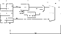
Fig. 2 shows the example data path 2 of the data handling system of the instruction that can be used for realizing Fig. 1.Register banks 4 contains 32 bit data word that will be handled.From above-mentioned register banks, read the input operand data word that is stored among Rm and the Rn, result data word is write back in the register Rd in the register banks 4.Data routing 2 comprises shift circuit 6 and adder circuit 8.Multiple other data processing instructions that said system provided uses shift circuit 6 and adder circuit 8 by different ways.This data routing 2 is carefully designed, and makes data value can be complementary with the data processing cycle time well via the time that shift circuit 6 and adder circuit 8 transmission are spent.Use the hardware resource of data routing 2 in system very fully, wherein, these resources all are movable concerning the major part of each data word of transmitting via data routing 2.Be provided with symbol/zero expansion and masking circuit 10 mutually concurrently with the low portion of shift circuit 6.Multiplexed 12 select the output of full shifting circuit 6 or the output conduct of symbol/zero expansion and masking circuit 10 to input to one of input of adder circuit 8.Other input to totalizer 8 is the input operand data word of Rn.
When the instruction of execution graph 1, the input operand data word of Rm is offered shift circuit 6, in this circuit, according in instruction, whether having specified parameter to make the optional right shift of 8 positions act on data word.Also can carry out the optional dextrad rotation of 16 and 24 positions.In shifter with multi-level multiplexer basis, the probability displacement that this strictness can be provided relatively simply from the first of shift circuit 6 is (for example with regard to 32 systems, the ground floor multiplexer can provide 16 displacement, and second layer multiplexer provides 8 Bit Shifts).Therefore, can be from via the value of extracting out the local path of shift circuit 6 with optional mode displacement specified amount, and provide it to symbol/zero expansion and masking circuit 10.Circuit 10 can be operated to cover us and fall the unselected multidigit part of input operand data word of the possible displacement of Rm, and assigns to replace the above-mentioned part that we falls of being covered with zero or sign extension of the multidigit part of the corresponding selection of these data words.The output of symbol/zero expansion and masking circuit 10 reaches first input of adder circuit 8 via multiplexer 12.Second input of adder circuit 8 is input operand data words of Rn.Adder circuit 8 carries out SIMD addition (promptly two 16 parallel additions effectively disconnect between the carry chain position 15 on the throne and 16) to its input.The output of adder circuit 8 is write back in the register Rd of register banks 4.
As another kind of form, symbol/zero expansion and masking circuit 10 can as its input, this circuit oneself carries out 0,8,16 or 24 rotation to four possible sign bits then with Rm (not rotation), and formation is covered worn-out.Shift circuit 6 is to operate with the mode that whole 32 Bit Shifts that make Rm walk abreast mutually.
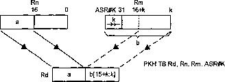
Fig. 3 and 4 has illustrated two kinds of versions of half-word packing SIMD type instruction.The PKHTB of Fig. 3 instruction get the fixed length that is stored in an input operand data word in the register Rn first half and be stored in second input operand data word among the register Rm variable position half bit position and the two is combined into after the corresponding first half-sum of the output data word that will be stored in the register Rd half.Instruction PKHBT get Rn input operand data word back half and Rm second input operand data word variable position half word length part and this two-phase is combined into back half-sum the first half of the output data word of Rd.As can be seen, the selected part of the input operand data word of Rn all not displacements on the position in output data word Rd in both cases.This just can be by simply covering worn-out or select circuit that this part is provided, thereby embody very little extra hardware expense.After the word of Rm had moved to right position, k position already, from the position 15 to 0, position of this word, select the part of half word of variable position of the instruction of Fig. 3.Similarly, after the word of Rm had moved to left position, k position already, from the position 31 to 16, position of this word, select variable position part according to half word length of the Rm of the Instruction Selection of Fig. 4.
Particularly useful with the variable displacement that provides with the packing function mode of combining of the instruction of Fig. 3 and Fig. 4 to the variation of " Q " value of regulating the point of fixity calculated value.Above-mentioned variation meeting occurs in these point of fixity calculated value processes of processing.
Fig. 5 has illustrated the data routing 14 that is specially adapted to execution graph 3 and Fig. 4 instruction.Register banks 4 provides once more to be the input operand data word of 32 bit data word in this example and output data word is stored.Above-mentioned data routing comprises shift circuit 6, adder circuit 8 and selection and combinational circuit 22.
In operation, the input operand data word of the not displacement of Rn directly reaches from deposit storehouse 4 and selects and combinational logic circuit 22.With regard to the instruction of Fig. 3, select the highest effective 16 and form corresponding positions among the output data word Rd of value of Rn.With regard to the instruction of Fig. 4, select minimum effective 16 and it is transmitted to form the least significant bit (LSB) of output data word Rd of input operand data word of Rn.The input operand data word of Rm is through full shifting circuit 6.With regard to the instruction of Fig. 3, carry out the arithmetic shift right of position, k position, then, by selecting and combinational circuit 22 chooses from the output of shift circuit 6 minimum effective 16, with minimum effective 16 of the output data word of formation Rd.With regard to the instruction of Fig. 4, shift circuit 6 provides the left-hand logical shift of position, k position and the result has been offered selection and combinational circuit 22.Select and combinational circuit 22 is selected the highest effective 16 and with the highest effective 16 of the output data word of these formation Rd of output of shift circuits 6.
As can be seen, select to be arranged on the position parallel mutually with adder circuit 8 with combinational circuit 22.Therefore, tentation data path 14 carefully is designed to can carry out full displacement and add operation in a processing cycle, then can be under the situation that does not apply any processing cycle limit, in the time cycle of the operation that allows to carry out adder circuit 8 usually, carry out comparatively directly selecting and combination operation.
Should be realized that, define above-mentioned data processing instructions according to the result who is obtained.Should be noted that available multiple different treatment step obtains identical end value with sequence of steps.Present invention includes all these versions that all these can produce same net result value with single instruction.
Claims (14)
1. equipment that is used for data processing, this equipment comprises:
Shift circuit;
Computing circuit; And
Instruction decoder, its response instruction and control above-mentioned shift circuit and computing circuit goes first Input Data word and second Input Data word are operated, wherein, described operation can produce the value that provides by following measures:
Select a plurality of non-adjacent multidigit part of above-mentioned first Input Data word, thereby form a plurality of multidigit parts, the bit length of each part is A;
By shared displacement above-mentioned a plurality of non-adjacent multidigit partial dislocations are become bit position after the displacement alternatively;
Make each part in above-mentioned a plurality of non-adjacent multidigit part all be promoted to bit length B, forming a plurality of multidigit parts that promoted, make that the described multidigit part that has promoted can be adjacent, thereby form the data word P that has promoted from bit length A; And
Will be from the position of the data word P of above-mentioned lifting and described second Input Data word long be the corresponding positions position part of B as input operand, carry out multiple independently arithmetic operation, with the formation result data word.
2. equipment as claimed in claim 1 is characterized in that B=2*A.
3. equipment as claimed in claim 1 is characterized in that, described a plurality of multidigit partial dislocations become the bit position after the displacement, so that the multidigit of lowest-order bit positions part is expanded since the zero bits position.
4. equipment as claimed in claim 1 is characterized in that, is that the A lifting is that B comprises one of following measures for bit length with above-mentioned multidigit part from bit length:
It is long with symbol above-mentioned multidigit partly to be extended to the B position; And
It is long with zero above-mentioned multidigit partly to be extended to the B position.
5. equipment as claimed in claim 1 is characterized in that, described a plurality of independently arithmetic operations are independently add operations.
6. equipment as claimed in claim 2 is characterized in that, it is long that each of described first data word and described second data word all has position, C position, C=N*B, and wherein, N is the integer greater than 1.
7. equipment as claimed in claim 6 is characterized in that C=B*2.
8. equipment as claimed in claim 1 is characterized in that, B=16 and A=8.
9. equipment as claimed in claim 1 is characterized in that, described shared displacement is B-A.
10. equipment as claimed in claim 1 is characterized in that, described instruction is the single instruction multiple data instruction.
11. equipment as claimed in claim 1 is characterized in that, data value is separated package operation in described instruction and arithmetic operation combines.
12. equipment as claimed in claim 1 is characterized in that, described shift circuit is positioned at the upstream of described computing circuit in the data routing of described equipment.
13. equipment as claimed in claim 1, it is characterized in that, one can operate in case with the described multidigit part lifting circuit that long A promotes the long B that puts in place from the position to be set up with the parallel mutually mode of the part of described shift circuit, when carrying out described instruction, described shift circuit can be operated, so that its scope is limited shared displacement when providing the shared displacement that provides when carrying out other instruction with described shift circuit to compare through the data value of this shift circuit.
14. the method for a data processing, this method comprises the following steps:
Instruction is decoded and carried out, and described instruction can produce the result who provides through the following steps:
Select a plurality of non-adjacent multidigit part of first data word, thereby form the multidigit part that a plurality of bit lengths are A;
By shared displacement described a plurality of non-adjacent multidigit partial dislocations are become bit position after the displacement alternatively;
Make each part in described a plurality of non-adjacent multidigit part all rise to bit length B, forming a plurality of multidigit parts that promoted, make that the described multidigit part that has promoted can be adjacent, thereby form the data word P that has promoted from bit length A; And
Will be from the position of the data word P of described lifting and second data word long be the corresponding positions position part of B as input operand, carry out multiple independently arithmetic operation, with the formation result data word.
Applications Claiming Priority (2)
| Application Number | Priority Date | Filing Date | Title |
|---|---|---|---|
| GB0024311.3 | 2000-10-04 | ||
| GB0024311A GB2367650B (en) | 2000-10-04 | 2000-10-04 | Single instruction multiple data processing |
Publications (2)
| Publication Number | Publication Date |
|---|---|
| CN1432151A CN1432151A (en) | 2003-07-23 |
| CN1196998C true CN1196998C (en) | 2005-04-13 |
Family
ID=9900674
Family Applications (1)
| Application Number | Title | Priority Date | Filing Date |
|---|---|---|---|
| CNB01810648XA Expired - Lifetime CN1196998C (en) | 2000-10-04 | 2001-08-21 | Single instruction multiple data processing |
Country Status (11)
| Country | Link |
|---|---|
| US (1) | US6999985B2 (en) |
| EP (1) | EP1323031B1 (en) |
| JP (1) | JP5133491B2 (en) |
| KR (1) | KR100880614B1 (en) |
| CN (1) | CN1196998C (en) |
| GB (1) | GB2367650B (en) |
| IL (2) | IL151395A0 (en) |
| MY (1) | MY129332A (en) |
| RU (1) | RU2279706C2 (en) |
| TW (1) | TW548587B (en) |
| WO (1) | WO2002029553A1 (en) |
Families Citing this family (14)
| Publication number | Priority date | Publication date | Assignee | Title |
|---|---|---|---|---|
| JP2003114323A (en) * | 2001-10-04 | 2003-04-18 | Bridgestone Corp | Near infarared ray absorbing film |
| JP3857614B2 (en) * | 2002-06-03 | 2006-12-13 | 松下電器産業株式会社 | Processor |
| US20030231660A1 (en) * | 2002-06-14 | 2003-12-18 | Bapiraju Vinnakota | Bit-manipulation instructions for packet processing |
| US8082419B2 (en) * | 2004-03-30 | 2011-12-20 | Intel Corporation | Residual addition for video software techniques |
| US7840954B2 (en) * | 2005-11-29 | 2010-11-23 | International Business Machines Corporation | Compilation for a SIMD RISC processor |
| US8290095B2 (en) * | 2006-03-23 | 2012-10-16 | Qualcomm Incorporated | Viterbi pack instruction |
| US8493979B2 (en) * | 2008-12-30 | 2013-07-23 | Intel Corporation | Single instruction processing of network packets |
| US8495341B2 (en) * | 2010-02-17 | 2013-07-23 | International Business Machines Corporation | Instruction length based cracking for instruction of variable length storage operands |
| GB2481384B (en) * | 2010-06-21 | 2018-10-10 | Advanced Risc Mach Ltd | Key allocation when tracing data processing systems |
| US8706795B2 (en) * | 2011-03-30 | 2014-04-22 | Intel Corporation | SIMD integer addition including mathematical operation on masks |
| US8604946B2 (en) * | 2011-04-08 | 2013-12-10 | Panasonic Corporation | Data processing device and data processing method |
| US20130113809A1 (en) | 2011-11-07 | 2013-05-09 | Nvidia Corporation | Technique for inter-procedural memory address space optimization in gpu computing compiler |
| CN103092571B (en) * | 2013-01-10 | 2016-06-22 | 浙江大学 | Support the single-instruction multiple-data arithmetical unit of numerous types of data |
| KR102182299B1 (en) * | 2019-07-24 | 2020-11-24 | 에스케이텔레콤 주식회사 | Device and Method for Performing Shift Operation |
Family Cites Families (10)
| Publication number | Priority date | Publication date | Assignee | Title |
|---|---|---|---|---|
| US4785393A (en) * | 1984-07-09 | 1988-11-15 | Advanced Micro Devices, Inc. | 32-Bit extended function arithmetic-logic unit on a single chip |
| DE69229324T2 (en) * | 1991-10-29 | 2000-02-24 | Advanced Micro Devices Inc | Arithmetic logic unit |
| US5673321A (en) * | 1995-06-29 | 1997-09-30 | Hewlett-Packard Company | Efficient selection and mixing of multiple sub-word items packed into two or more computer words |
| US6237016B1 (en) * | 1995-09-05 | 2001-05-22 | Intel Corporation | Method and apparatus for multiplying and accumulating data samples and complex coefficients |
| US5835782A (en) * | 1996-03-04 | 1998-11-10 | Intel Corporation | Packed/add and packed subtract operations |
| US5812140A (en) * | 1996-09-05 | 1998-09-22 | Adobe Systems Incorporated | Efficient gray tile storage |
| US6061783A (en) * | 1996-11-13 | 2000-05-09 | Nortel Networks Corporation | Method and apparatus for manipulation of bit fields directly in a memory source |
| US6081824A (en) * | 1998-03-05 | 2000-06-27 | Intel Corporation | Method and apparatus for fast unsigned integral division |
| JPH11272546A (en) * | 1998-03-23 | 1999-10-08 | Nec Corp | Variable length register device |
| US6338135B1 (en) * | 1998-11-20 | 2002-01-08 | Arm Limited | Data processing system and method for performing an arithmetic operation on a plurality of signed data values |
-
2000
- 2000-10-04 GB GB0024311A patent/GB2367650B/en not_active Expired - Lifetime
-
2001
- 2001-08-21 IL IL15139501A patent/IL151395A0/en unknown
- 2001-08-21 EP EP01960902.3A patent/EP1323031B1/en not_active Expired - Lifetime
- 2001-08-21 KR KR1020037004621A patent/KR100880614B1/en active IP Right Grant
- 2001-08-21 RU RU2002124769/09A patent/RU2279706C2/en not_active IP Right Cessation
- 2001-08-21 WO PCT/GB2001/003744 patent/WO2002029553A1/en active Application Filing
- 2001-08-21 JP JP2002533059A patent/JP5133491B2/en not_active Expired - Lifetime
- 2001-08-21 CN CNB01810648XA patent/CN1196998C/en not_active Expired - Lifetime
- 2001-08-29 TW TW090121381A patent/TW548587B/en not_active IP Right Cessation
- 2001-08-30 US US09/941,790 patent/US6999985B2/en not_active Expired - Lifetime
- 2001-09-21 MY MYPI20014440A patent/MY129332A/en unknown
-
2002
- 2002-08-21 IL IL151395A patent/IL151395A/en active IP Right Grant
Also Published As
| Publication number | Publication date |
|---|---|
| US6999985B2 (en) | 2006-02-14 |
| JP5133491B2 (en) | 2013-01-30 |
| US20020040378A1 (en) | 2002-04-04 |
| KR20030066631A (en) | 2003-08-09 |
| EP1323031B1 (en) | 2018-11-14 |
| TW548587B (en) | 2003-08-21 |
| GB2367650A (en) | 2002-04-10 |
| MY129332A (en) | 2007-03-30 |
| JP2004511039A (en) | 2004-04-08 |
| GB0024311D0 (en) | 2000-11-15 |
| IL151395A (en) | 2009-09-01 |
| EP1323031A1 (en) | 2003-07-02 |
| RU2002124769A (en) | 2004-02-20 |
| RU2279706C2 (en) | 2006-07-10 |
| WO2002029553A1 (en) | 2002-04-11 |
| IL151395A0 (en) | 2003-04-10 |
| CN1432151A (en) | 2003-07-23 |
| GB2367650B (en) | 2004-10-27 |
| KR100880614B1 (en) | 2009-01-30 |
Similar Documents
| Publication | Publication Date | Title |
|---|---|---|
| CN1196998C (en) | Single instruction multiple data processing | |
| KR100715770B1 (en) | Method and a system for performing calculation operations and a device | |
| US5448509A (en) | Efficient hardware handling of positive and negative overflow resulting from arithmetic operations | |
| KR100714358B1 (en) | Method and system for performing calculation operations and a device | |
| US6601077B1 (en) | DSP unit for multi-level global accumulation | |
| WO2001035224A1 (en) | Bit-serial memory access with wide processing elements for simd arrays | |
| CN110705703B (en) | Sparse neural network processor based on systolic array | |
| JP3938238B2 (en) | Fast Fourier transform processor | |
| KR100289513B1 (en) | Calculation device and calculation and accumulation device of population count | |
| CN110851779B (en) | Systolic array architecture for sparse matrix operations | |
| US20030097391A1 (en) | Methods and apparatus for performing parallel integer multiply accumulate operations | |
| EP2232361A1 (en) | Method and instruction set including register shifts and rotates for data processing | |
| CN1218240C (en) | Arithmetic operations in data processing system | |
| US5726926A (en) | Shifter for shifting floating point number utilizing arithmetic operation of redundant binary number, and adder containing the same | |
| Sima et al. | An 8x8 IDCT Implementation on an FPGA-augmented TriMedia | |
| US7260711B2 (en) | Single instruction multiple data processing allowing the combination of portions of two data words with a single pack instruction | |
| KR20100139072A (en) | Polynomial data processing operation | |
| Zucker et al. | Reuse of high precision arithmetic hardware to perform multiple concurrent low precision calculations | |
| US20080071852A1 (en) | Method to perform a subtraction of two operands in a binary arithmetic unit plus arithmetic unit to perform such a method | |
| KR100284883B1 (en) | Real or complex multiplier | |
| KR20050084681A (en) | Method and a system for performing a multiplication operation and a device | |
| JP2000231552A (en) | High speed fourier transformation method | |
| JP2001084242A (en) | Variable operation processor | |
| WO2001088691A2 (en) | Method and apparatus of dsp resource allocation and use | |
| Roy | Design of Multiplier Circuits |
Legal Events
| Date | Code | Title | Description |
|---|---|---|---|
| C06 | Publication | ||
| PB01 | Publication | ||
| C10 | Entry into substantive examination | ||
| SE01 | Entry into force of request for substantive examination | ||
| C14 | Grant of patent or utility model | ||
| GR01 | Patent grant | ||
| CX01 | Expiry of patent term | ||
| CX01 | Expiry of patent term |
Granted publication date: 20050413 |