CN116033276A - Image sensor - Google Patents
Image sensor Download PDFInfo
- Publication number
- CN116033276A CN116033276A CN202211294721.9A CN202211294721A CN116033276A CN 116033276 A CN116033276 A CN 116033276A CN 202211294721 A CN202211294721 A CN 202211294721A CN 116033276 A CN116033276 A CN 116033276A
- Authority
- CN
- China
- Prior art keywords
- column
- amplifier
- image sensor
- voltage
- pixels
- Prior art date
- Legal status (The legal status is an assumption and is not a legal conclusion. Google has not performed a legal analysis and makes no representation as to the accuracy of the status listed.)
- Pending
Links
Images


Classifications
-
- H—ELECTRICITY
- H04—ELECTRIC COMMUNICATION TECHNIQUE
- H04N—PICTORIAL COMMUNICATION, e.g. TELEVISION
- H04N25/00—Circuitry of solid-state image sensors [SSIS]; Control thereof
- H04N25/70—SSIS architectures; Circuits associated therewith
- H04N25/76—Addressed sensors, e.g. MOS or CMOS sensors
- H04N25/78—Readout circuits for addressed sensors, e.g. output amplifiers or A/D converters
-
- H—ELECTRICITY
- H04—ELECTRIC COMMUNICATION TECHNIQUE
- H04N—PICTORIAL COMMUNICATION, e.g. TELEVISION
- H04N25/00—Circuitry of solid-state image sensors [SSIS]; Control thereof
- H04N25/70—SSIS architectures; Circuits associated therewith
- H04N25/76—Addressed sensors, e.g. MOS or CMOS sensors
- H04N25/767—Horizontal readout lines, multiplexers or registers
-
- H—ELECTRICITY
- H04—ELECTRIC COMMUNICATION TECHNIQUE
- H04N—PICTORIAL COMMUNICATION, e.g. TELEVISION
- H04N25/00—Circuitry of solid-state image sensors [SSIS]; Control thereof
- H04N25/60—Noise processing, e.g. detecting, correcting, reducing or removing noise
- H04N25/65—Noise processing, e.g. detecting, correcting, reducing or removing noise applied to reset noise, e.g. KTC noise related to CMOS structures by techniques other than CDS
-
- H—ELECTRICITY
- H04—ELECTRIC COMMUNICATION TECHNIQUE
- H04N—PICTORIAL COMMUNICATION, e.g. TELEVISION
- H04N25/00—Circuitry of solid-state image sensors [SSIS]; Control thereof
- H04N25/70—SSIS architectures; Circuits associated therewith
- H04N25/76—Addressed sensors, e.g. MOS or CMOS sensors
- H04N25/77—Pixel circuitry, e.g. memories, A/D converters, pixel amplifiers, shared circuits or shared components
- H04N25/772—Pixel circuitry, e.g. memories, A/D converters, pixel amplifiers, shared circuits or shared components comprising A/D, V/T, V/F, I/T or I/F converters
-
- H—ELECTRICITY
- H04—ELECTRIC COMMUNICATION TECHNIQUE
- H04N—PICTORIAL COMMUNICATION, e.g. TELEVISION
- H04N25/00—Circuitry of solid-state image sensors [SSIS]; Control thereof
- H04N25/70—SSIS architectures; Circuits associated therewith
- H04N25/76—Addressed sensors, e.g. MOS or CMOS sensors
- H04N25/77—Pixel circuitry, e.g. memories, A/D converters, pixel amplifiers, shared circuits or shared components
- H04N25/778—Pixel circuitry, e.g. memories, A/D converters, pixel amplifiers, shared circuits or shared components comprising amplifiers shared between a plurality of pixels, i.e. at least one part of the amplifier must be on the sensor array itself
Abstract
An image sensor for an electronic camera having a plurality of pixels for generating exposure-related signals, wherein a respective pixel comprises at least one photosensitive element; a read-out node; a transmission gate; a converter transistor; and a select switch connected to a signal output of the converter transistor to selectively couple the signal output to a column line of the image sensor. The column lines are coupled or couplable via input capacitors to the negative inputs of associated column amplifiers, with the amplifier outputs of the column amplifiers connected to column readout circuitry and compensation lines. The compensation lines are coupled to respective readout nodes of the associated pixels via respective feedback capacitors.
Description
Technical Field
The present invention relates to an image sensor for an electronic camera, and in particular, to a CMOS image sensor including a plurality of pixels for generating exposure-related signals.
Background
Electronic cameras are used, for example, as movie cameras to record movie sequences that are later displayed in a theatre. In this respect, it is important that these cameras have high image quality. The recorded images also change in brightness, contrast and color, especially during post-production, and the end product (processed film sequence or film) is projected onto a large screen in the theatre.
Electronic cameras typically use image sensors composed of silicon in CMOS or CCD technology. In such an image sensor, pixels form a pixel field, and they are arranged in rows and columns. The pixels may provide a color filter array (color filter array, CFA) to have different spectral sensitivities. Each pixel comprises at least: a photosensitive element that generates charge from incident light; an additional sense node; a transfer gate selectively coupling the photosensitive element to the readout node and transferring the generated charge from the photosensitive element to the readout node; a converter transistor that converts the charge present at the sense node into a voltage signal at the signal output; and a select switch connected to the signal output of the converter transistor via an output line to selectively couple the signal output of the converter transistor to an associated sense line (which is commonly designated as a column line) of the image sensor.
Each pixel may also include a reset switch to selectively couple the readout node to a reset potential. Such an image sensor may further comprise control circuitry for generating control signals for the respective transfer gates, for the respective selection switches and, if applicable, for the respective reset switches of the pixels for selectively reading out the image signals (or the image signal and the reference signal) from the read-out node. The converter transistor may form an impedance converter that generates a voltage signal at its signal output in dependence on the amount of charge present at its input. The column lines of the image sensor may be connected to respective sense amplifiers (commonly referred to as column amplifiers) to selectively couple the signal outputs of the converter transistors to the column lines of the image sensor associated with the plurality of pixels of the image sensor. The plurality of column lines of the image sensor may also be connected to a signal bus that leads to one or more column amplifiers to amplify the (possibly pre-amplified) voltage signals of the plurality of column lines. The pixels of the image sensor are addressed, for example, row by row, and the signals of the pixels are conducted to column amplifiers (e.g., at the edges of the pixel field), and from the column amplifiers to the output, the signals of the pixels are digitized and optionally offset with calibration data.
In order to be able to record film sequences in poor lighting conditions and to keep artificial illumination measurements on film sets at low cost, it is desirable that the image sensor of the electronic camera has a high light sensitivity.
Disclosure of Invention
It is an object of the present invention to provide an image sensor with improved image quality.
The present invention is based on the following considerations.
The light sensitivity is roughly determined by the noise of the image sensor. The lowest signal range is particularly critical in poor lighting conditions. The noise of the image sensor is substantially composed of the noise of the corresponding pixel and the noise of the readout path. By proper design, the noise of the readout path can be reduced to a value of, for example, 80 μv (microvolts), so that it only plays a subordinate role compared to, for example, 180 μv pixel noise.
The noise voltage in the respective pixel is substantially determined by the converter transistor (e.g., source follower, SF). The noise of a pixel is the ratio between the electronically induced signal voltage and the noise voltage of the converter transistor (SF). In order to reduce noise, it is therefore necessary to reduce the noise voltage of the converter transistor, or to increase the electron-induced signal voltage (so-called tilt).
When photons are absorbed into a photosensitive element, such as a pin diode, electrons are generated there. Due to the transfer gate of the transient control pixel, this electron is transferred to the readout node (e.g., floating diffusion, FD) (where typically multiple photo-generated electrons are transferred during readout). The charge of the corresponding electron acts on the capacitance of the sense node (FD) and causes a voltage change therein that is inversely proportional to the capacitance of the sense node. In order to increase the signal voltage caused by electrons and thereby reduce noise of the pixel, it is thus possible to try to reduce the capacitance of the readout node (FD).
In a typical image sensor, the readout node of the corresponding pixel may have a capacitance of, for example, 1.6fF (femto farad), thereby achieving a voltage variation of about 100 μV per electron. For example, the FD capacitance may be reduced to 0.6fF by further methods (e.g., using a protective structure), whereby a voltage change of about 260 μv per electron may be achieved.
However, it is desirable to further reduce noise. This can be achieved by further reducing the capacitance of the sense node, and thus by increasing the signal voltage caused by electrons at the sense node. The capacitance of the sense node is essentially the parasitic capacitance to ground. Thus, this capacitance is not effective or as small as possible, and the voltage at the sense node must remain constant. However, when electrons are transferred from the photosensitive element to the sense node and thereby cause a voltage change at the sense node, the voltage change in turn affects the capacitance of the sense node. In order to significantly increase the sensitivity of the image sensor, the voltage at the sense node must therefore be kept constant in order to achieve a low capacitance at the sense node and thus a higher signal voltage per electron and also to maintain this higher signal voltage when charge is transferred to the sense node.
The object is met by an image sensor having the features of claim 1.
In this image sensor, a column amplifier is associated with a column line, where the column line is coupled to or can be coupled (e.g., via a switch) to a negative input of the column amplifier via an input capacitor. The column amplifier has an amplifier output for outputting an amplifier output signal, wherein the amplifier output is connected to the column readout circuit and the compensation line. The compensation line may also be designated as compensation line. The compensation lines are coupled via respective feedback capacitors to respective readout nodes of those pixels associated with the column lines.
Thus, the voltage signal generated at the signal output of the converter transistor of the respective pixel can be effectively capacitively fed back to the readout node of the respective pixel. In other words, an inverted feedback loop is formed comprising the column line, the input capacitor, the column amplifier (via its negative input), the compensation line and the feedback capacitor.
A feedback capacitor (indirectly) coupled or couplable to the readout node ensures that in case of a charge transfer from the photosensitive element to the readout node of the respective pixel, it is possible to adjust the voltage of the readout node by means of the column amplifier or the amplifier output. In particular, the voltage at the sense node may be adjusted such that there is a reduced capacitance at the sense node. Thus, an increased signal voltage per electron can be achieved at the readout node of the respective pixel.
Thus, the feedback capacitor determines the signal voltage per electron and thus the sensitivity of the pixel. The required signal voltage per electron can be achieved by the feedback and the corresponding dimensions of the feedback capacitor. To obtain a signal voltage of, for example, 4000 μv per electron, a capacitance of the sense node of about 40aF (atto farad) is required. In this respect the size of the feedback capacitor can be very small, since in particular the capacitance between the column line and the sense node is decisive.
The above values are to be understood as exemplary. The effect achieved by the feedback capacitor may also be stronger or weaker.
This active limitation of the capacitance of the sense node is particularly applicable to low signal strengths in poor light conditions, i.e. to small amounts of electrons transferred from the photosensitive element to the sense node each time the transfer gate is driven. The photosensors of the individual pixels can also be read out in succession in this way in a number of repetitions, wherein partial results are obtained which can be superimposed. In contrast, for larger amounts of charge in the photosensitive element, conventional readout methods can be used without the need for the explained feedback back through the feedback capacitor.
The invention may also be used with more complex pixel architectures and/or readout architectures than those described above. For example, an overflow capacitor with an additional transfer gate may be provided within each pixel, as will be explained below. In some embodiments, the respective pixel may further comprise a plurality of photosensitive elements connected or couplable to a common readout node (FD) (so-called "sharing") via respective transfer gates and/or associated (alternating in time) with a common converter transistor. Further, the image sensor may have a plurality of column lines for each column of pixels, wherein the plurality of column lines may be coupled or couplable to a common column amplifier via a signal bus. Furthermore, multiple channels with different gain factors may be provided for each pixel.
If reference is made to a voltage or potential in connection with the present invention, then the voltage must be considered as the difference between a first potential (e.g., the generated or considered potential) and a second potential (e.g., the reference potential). These two terms may ultimately be identical or used in an identical manner in this respect if the corresponding reference potentials are given.
If reference is made herein to lines in an image sensor in connection with the present invention, it is understood here that the conductive connection may be formed in particular on or within the substrate, for example by metallization or doping.
Other embodiments of the present invention will be explained below.
In some embodiments, the column amplifier may be configured to generate an amplifier output signal from the voltage signal of the converter transistor of the respective pixel received at the input capacitor via the column line, and to output the amplifier output signal to the column readout circuit and to the feedback capacitor via the compensation line.
For example, when the selection switch is opened, the voltage generated at the sense node may be output as a voltage signal to the column line via the converter transistor. The voltage signal at the column line may particularly follow (particularly as a proportional value) the voltage generated at the readout node of the respective pixel, e.g. due to charge transfer via the transfer gate. The voltage difference that exists between the column line and the negative input of the column amplifier may ensure that the input capacitor arranged between the column line and the negative amplifier input charges according to the voltage difference. Depending on the mode of operation of the column amplifier, the amplifier output signal may take different values, as will be explained further below. The amplifier output signal is sent to the column readout circuit and to the feedback capacitor via the compensation line. The column readout circuit may output a corresponding signal value that ultimately corresponds to the image information. The explained reverse feedback loop to the respective sense node may be formed via the compensation line and the feedback capacitor.
In some embodiments, the column readout circuitry may be configured to sense the amplifier output signal. In particular, the column readout circuit may be configured to output a signal value corresponding to the amplifier output signal.
In some embodiments, in particular, the column readout circuit may be configured to read out the reference signal and the image signal as amplifier output signals and offset them from each other (in particular by subtraction) to cancel offset values (so-called correlated double sampling), as will be explained further below.
In some embodiments, the converter transistor, column line, input capacitor, column amplifier, compensation line, and feedback capacitor of the respective pixel may form an inverted feedback loop for the readout node of the respective pixel. Due to such a reverse feedback loop, an undesired increase of the voltage due to charge transfer and thus of the capacitance of the sense node can be counteracted.
In particular, the input capacitor, the column amplifier and the feedback capacitor of the respective pixel may be configured (arranged and dimensioned) to keep the voltage at the readout node of the respective pixel substantially constant.
This reverse feedback does not have to occur permanently. However, the column amplifier may also form a temporary feedback via only said elements. For the period of feedback, the column amplifier may adjust the voltage at the compensation line such that in case of charge transfer (from the photosensitive element via the transfer gate) the voltage at the readout node of the respective pixel remains substantially constant as well.
In some embodiments, in the event that the charge at the readout node of the respective pixel increases, the input capacitor, the column amplifier, and the feedback capacitor of the respective pixel may be configured to increase the voltage at the compensation line and thereby substantially compensate for the voltage change at the readout node. This feedback may take advantage of the fact that the voltage at the column line follows the voltage at the sense node and the voltage at the column line is also available at the column amplifier via the input capacitor.
In some embodiments, the column amplifier may include a positive amplifier input to which a reference voltage is applied in addition to a negative amplifier input. The reference voltage may be used in particular as a reference value to perform the explained feedback in reverse and to improve the accuracy of the measurement. Due to the negative feedback, the reference voltage may be reflected in particular onto the negative amplifier input, so that the negative amplifier input and the input capacitor connected to the negative amplifier input are defined as starting values for the subsequent measurement.
In particular, the column amplifier may comprise an operational amplifier having a negative amplifier input and a positive amplifier input.
In some embodiments, the negative amplifier input of the column amplifier may be connected to the amplifier output via a negative feedback line and a negative feedback switch, wherein by closing the negative feedback switch the column amplifier may be put into a negative feedback mode in which the potential difference between the voltage at the column line and the reference voltage is set at the input capacitor. The column amplifier may in particular operate as a voltage follower in a negative feedback mode, i.e. the amplifier output signal may correspond to the input voltage at the positive input of the column amplifier, i.e. to the applied reference voltage.
By subsequently opening the negative feedback switch, the column amplifier can start from a negative feedback mode into an amplifying mode in which the amplifier output signal represents a potential difference at the input capacitor that changes relative to the negative feedback mode. The change in the potential difference at the input capacitor may be caused by, inter alia, an intermediate charge transfer from the photosensitive element to the read-out node of the respective pixel and a corresponding change in the voltage signal of the respective converter transistor. In the amplification mode of the column amplifier, the amplifier output signal may thus represent a voltage change at the readout node of the respective pixel and thus the number of electrons transferred to the readout node. In particular, in the amplifying mode, the column amplifier may operate as a differential amplifier.
In some embodiments, the image sensor may have control circuitry configured to first put the column amplifier into a negative feedback mode to read out the corresponding pixel; subsequently causing the column amplifier to enter an amplification mode; thereafter, the transfer gate of the corresponding pixel is at least partially turned on for a short period of time to transfer charge to the readout node of the corresponding pixel; the column readout circuit is then controlled to read out the amplifier output signal, which then represents the signal value or image signal value of the corresponding pixel. The control circuit may comprise, for example, an integrated circuit, a microprocessor, or an FPGA.
During this type of global readout, the selection switch of the corresponding pixel may be closed. As already explained, the negative feedback mode may be started by closing the negative feedback switch. The input capacitor can be brought into a defined start value by a negative feedback mode. The amplification mode may then be initiated by opening the negative feedback switch. In the amplification mode, the amplifier output signal may represent the charge transferred to the readout node of the corresponding pixel. Furthermore, the column amplifier may be in a feedback mode during the amplifying mode, i.e. the amplifier output signal is capacitively fed back to the readout node of the respective pixel via the compensation line and the feedback capacitor.
In some embodiments, the respective pixel may also have a reset switch for selectively coupling the readout node to a reset potential. The control circuit may be configured to briefly close the reset switch of the respective pixel to remove charge present in the readout node of the respective pixel; then, in the amplifying mode of the column amplifier, and before controlling (i.e., turning on) the transfer gate, the column readout circuit is controlled to read out an amplifier output signal, which then represents the reference value or reference signal value of the corresponding pixel.
Based on the read reference value, the magnitude of the voltage change resulting from the transfer of charge to the read node can be determined with greater accuracy. In particular, a reference value (determined with the transmission gate open) can be subtracted from the signal value (so-called correlated double sampling).
In some embodiments, the column readout circuit may have a reference value readout path and a signal value readout path for this purpose. In particular, the reading out of the reference value may be performed via a reference value reading out path, and in particular the reading out of the signal value may be performed via a signal value reading out path, wherein the reading out of the reference value and the reading out of the signal value may be performed at different points in time.
In some embodiments, the respective pixel may further include an overflow capacitor and another transfer gate selectively coupling the readout node to the overflow capacitor. Thus, the capacitance of the pixel can be selectively temporarily increased so as to be able to receive a large charge amount from the photosensitive element at the time of high exposure. The control circuit may be further configured to generate a control signal for another transmission gate.
Drawings
The present invention will be described below with reference to the embodiments and the drawings, wherein the same elements or the same type of elements are characterized by the same reference numerals.
FIG. 1 shows a four transistor CMOS image sensor; in the image sensor, only one pixel and a column amplifier circuit associated with a column line of the pixel are shown;
FIG. 2 shows an image sensor according to the invention in a representation corresponding to FIG. 1;
FIG. 3 shows an alternative embodiment of a corresponding pixel of the image sensor according to FIG. 2; and
fig. 4 shows a circuit diagram of a control circuit of an image sensor according to the present invention.
List of reference numerals
10. Pixel arrangement
20. Photosensitive element
21. Transmission gate
22. Readout node
23. Parasitic capacitance
24. Converter transistor
25. Selection switch
26. Reset switch
27. Voltage source terminal
28. Feedback capacitor
29. Signal output of converter transistor
30. Overflow capacitor
31. Another transmission gate
40. Control circuit
41. Column line
42. Compensation line
60. Amplifier circuit for small charge amounts
61. 81 input capacitor
62. Power source
63. 83 voltage node
64. 84 amplifier capacitor
85. Column amplifier
66. 86 negative feedback switch
67. Negative input of column amplifier
68. Positive input of column amplifier
69. Amplifier output
70. Column readout circuit
71. 91 signal value switch
72. 92 signal value capacitor
73. 93 reference value switch
74. 94 reference capacitor
80. Amplifier circuit for large charge quantity
Detailed Description
For a better understanding of the invention, the basic operation of an exemplary four transistor image sensor of the APS (active pixel sensor) type, wherein the individual components of the image sensor are also present in the image sensor according to the invention, will be explained below with reference to fig. 1. However, in general, the present invention is not limited to active four transistor image sensors, but may also be used for image sensors having fewer or more than four transistors per pixel, as will be explained below.
In fig. 1 only a single pixel 10 is shown, which pixel comprises a light sensitive element 20 in the form of a photodiode, in particular in the form of a so-called pin diode. The photosensitive element 20 is selectively charge-coupled to a sense node 22 via a switch in the form of a transfer gate 21, which sense node 22 may be formed, in particular, as a so-called floating diffusion (floating diffusion, FD).
The readout node 22 is connected to a gate terminal of a converter transistor 24 configured as a source follower, which converter transistor 24 is formed by a Field Effect Transistor (FET) and represents a charge-voltage converter circuit. Further, the sense node 22 is connected via a further switching device in the form of a reset switch 26 to a terminal 27 of a voltage source VDD (e.g. a positive voltage source). One of the two channel terminals (drain terminal) of the converter transistor 24 is likewise connected to the positive voltage source VDD, while the other of the two channel terminals (source terminal) of the converter transistor 24 forms a signal output 29, at which signal output 29 a voltage signal is output, and which signal output 29 is connected to the selection switch 25. The selection switch 25 functions as a row selection switch, wherein the signal output 29 of the converter transistor 24 can be selectively coupled to a column line 41 associated with the represented pixel 10 by activating or closing the selection switch 25.
A column line 41 (COL) is provided to connect a plurality or all of the pixels 10 of the same type arranged in the relevant column to a common column amplifier circuit 60, which common column amplifier circuit 60 is arranged, for example, outside the pixel field of the image sensor. This is done in an alternating manner by temporarily closing the respective selection switches 25 of the pixels 10.
A precharge circuit including a power supply 62 is also associated with the column line 41 outside the pixel field of the image sensor.
The transfer gates 21 of the respective pixels 10 are controllable via control lines TG1 by a common control circuit 40 of the image sensor; the reset switch 26 is controllable via a control line RES; the selection switch 25 is controllable via a control line SEL; the negative feedback switch 66 is controllable via control line FB; the reference value switch 73 is controllable via a control line SHR; and a controllable signal value switch 71 via control line SHS.
The principle of operation of such a pixel 10 will be described below by way of example based on 3.3V CMOS technology. This process is also referred to as "correlated double sampling (correlated double sampling, CDS)". In general, all pixels 10 in a row are read out in the same way and in particular in parallel, so that it is sufficient for the description of the read-out process to look at only those pixels 10 which are connected to the same column line 41.
Light incident during exposure is converted into electric charge by the photosensitive element 20 of the corresponding pixel 10, so that the photosensitive element 20 is filled with electrons. During exposure, the control lines TG1, SEL and RES are each kept at 0V, i.e. the switches 21, 24, 26 controlled thereby are open.
A voltage of 3.3V is briefly applied to the control line RES prior to the actual readout of the individual pixels 10 to remove charge formed by leakage currents and/or scattered light from the readout node 22, i.e. to delete the readout node 22. Thus, sense node 22 is set to a start state defined by voltage source VDD. Thus, a voltage corresponding to the charge at the erased sensing node 22 is employed at the signal output 29 of the converter transistor 24.
Further, a voltage of 3.3V is applied to the control line FB to close the negative feedback switch 66, so that the column amplifier 65 is negatively coupled. Thus, the voltage of VREF is taken at the negative input 67 of the column amplifier 65 and thus at the voltage node 63 and at the relevant terminal of the input capacitor 61.
To read out the reference value, a voltage of 3.3V is applied to the control line SEL, so that the selection switch 25 is closed. Thus, the voltage signal of the converter transistor 24 corresponding to the charge in the sense node 22 is switched to the column line 41 via the selection switch 25 and thus to the input capacitor 61. Thus, the input capacitor 61 is charged to the potential difference between the reference voltage VREF and the voltage at the column line 41. Further, the negative feedback switch 66 is turned off (the control line FB is set to 0V). Due to the switching process, small disturbances (e.g., charge injection) are generated. The column amplifier 65 is readjusted accordingly. A voltage of 3.3V is now briefly applied to the control line SHR to close the reference value switch 73 and thereby charge the reference value capacitor 74 in accordance with the amplifier output signal. After the reference value switch 73 is opened again, the reference value can thus be read out from the reference value capacitor 74.
For reading out the signal value, a voltage of 3.3V or less is then briefly applied to the control line TRF to at least temporarily open the transfer gate 21 of the respective pixel 10 for a short period of time, or to close the switch formed thereby, so that electrons generated in accordance with the exposure can be transferred from the photosensitive element 20 to the readout node 22. The changed voltage signal of the converter transistor 24 corresponding to the changed charge in the sense node 22 is transferred via the selection switch 25 (again or still closed) to the column line 41 and thus to the input capacitor 61. The column amplifier 65 amplifies the altered signal with the capacitance ratio of the input capacitor 61 and the amplifier capacitor 64 (the negative feedback switch 66 remains open) and generates a corresponding altered amplifier output signal at the amplifier output 69. Thus, a voltage is now applied to the output 69 of the column amplifier 65, which voltage starts at the start state (bias value) of the sense node 22, corresponding to the voltage change (voltage drop) due to the transfer of charge from the photosensitive element 20 to the sense node 22. A voltage of 3.3V is briefly applied to the control line SHS to close the signal value switch 71 and thereby charge the signal value capacitor 72 according to the changed amplifier output signal. After the signal value switch 71 is turned off again, the signal value (image signal value) can be read out from the signal value capacitor 72.
The difference between the read reference value and the signal value corresponds to the amount of charge transferred from the photosensitive element 20 to the read node 22 by opening the transfer gate 21.
Thereafter, if necessary, a voltage of 3.3V may be applied to the control line RES again briefly to remove the current charge from the readout node 22, and the explained readout process is repeated for a further partial charge quantity, which is transferred from the photosensitive element 20 to the readout node 22 (readout reference value and signal value) by opening the transfer gate 21 more.
Finally, a voltage of 3.3V may also be briefly applied to control lines RES and TG1 to remove the charge from readout node 22 and any residual charge from photosensitive element 20 so that the next exposure process may be restarted with a completely "empty" pixel 10.
These steps will also be performed for other pixels 10 connected to the respective column line 41.
Fig. 2 shows parts of an image sensor according to the invention, in which again a four transistor image sensor is shown by way of example, and only a single pixel 10 is shown as a representative even if the image sensor has a plurality of pixels 10 arranged in rows and columns. In particular, the main differences from the image sensor according to fig. 1 will be explained below.
The difference from the image sensor according to fig. 1 is that in addition to the column lines 41 the individual pixels 10 are coupled to compensation lines 42 (CMP), which compensation lines 42 extend parallel to the column lines 41 and are associated with columns of pixels 11, similar to the column lines 41. The compensation line 42 is connected at one end to an amplifier output 69 of a column amplifier 65 of the associated column line 41. At the other end, the compensation line 42 branches to the pixel 11 associated with the column line 41 and is capacitively coupled to the readout node 22 of the respective pixel 10 via the respective feedback capacitor 28.
Another difference from the image sensor according to fig. 1 is that no amplifier capacitor 64 is provided between the negative input 67 of the column amplifier 65 and the amplifier output 69, but only a negative feedback switch 66.
The image sensor according to fig. 2 is capable of operating with high light sensitivity even with small amounts of charge transferred from the photosensitive element 20 to the readout node 22 of the respective pixel 10, so that film sequences can be recorded even in poor lighting conditions. This is achieved by a high sensitivity (inclination of the gain characteristic) of the corresponding sense node 22.
The converter transistor 24, the column line 41, the input capacitor 61, the column amplifier 65, the compensation line 42 and the feedback capacitor 28 of the respective pixel 10 form a respective inverted feedback loop for the readout node 22 of the respective pixel 10. As a result of the reverse feedback loop, the voltage change in sense node 22 caused by the charge carriers transferred from photosensitive element 20 to sense node 22 is compensated by the active feedback of amplifier output 69 to sense node 22. In particular, column amplifier 65 may offset the voltage drop at sense node 22 by increasing the voltage at amplifier output 69 or at compensation line 42, so that the voltage at sense node 22 may remain substantially constant due to capacitive coupling via feedback capacitor 28. Thus, the parasitic capacitance at the sense node 22 (shown by reference numeral 23 in fig. 2) becomes substantially ineffective. Thus, the gain characteristics are not compromised by the charge carriers transferred to the sense node 22 and the resulting increase in (parasitic) capacitance.
Since the feedback capacitor 28 has a size of, for example, 40aF or less, a signal voltage of about 4000 μv per electron can be realized in the sense node 22, which corresponds to a noise value of 0.05 electrons. As an example, a MIM (metal-insulator-metal) capacitor may be used as the feedback capacitor 28 by using the capacitance between two line ends.
Similar to what is explained for the image sensor according to fig. 1, for reading out the respective pixel 10, the negative feedback mode of the column amplifier 65 can first take place to set the input capacitor 61 to a defined starting value, and subsequently the amplification mode of the column amplifier 65 can take place. In the amplifying mode, column amplifier 65 may generate an amplifier output signal from the voltage signal of converter transistor 24 received at input capacitor 61 via column line 41 and output the amplifier output signal to feedback capacitor 28 via compensation line 42.
A viable readout procedure will be described below.
A voltage of 3.3V is briefly applied to the control line RES before the actual readout of the corresponding pixel 10 to briefly close the reset switch 26 and delete the readout node 22 (the start state of the readout node 22). Thus, a voltage corresponding to the (residual) charge at the erased sensing node 22 is applied at the signal output 29 of the converter transistor 24. A voltage of 3.3V is further applied to the control line FB to close the negative feedback switch 66 so that the column amplifier 65 is negatively coupled. Thus, the voltage of VREF is taken at the negative input 67 of the column amplifier 65 and thus at the voltage node 63 and at the associated terminal of the input capacitor 61.
To read out the reference value, a voltage of 3.3V is applied to the control line SEL, so that the selection switch 25 is closed. The voltage signal of the converter transistor 24 corresponding to the charge in the sense node 22 or to the starting state of the sense node 22 is thereby connected to the column line 41 via the selection switch 25 and thus to the input capacitor 61. Thus, the input capacitor 61 is charged to the potential difference between the reference voltage VREF of the column amplifier 65 and the voltage at the column line 41.
In addition, the negative feedback switch 66 is open. Due to the switching process, small disturbances (e.g., charge injection) are generated. The column amplifier 65 is readjusted according to the voltage difference present at the two inputs 67, 68. At this point in time a voltage of 3.3V is applied to the control line SHR or is now applied to close the reference value switch 73, thereby charging the reference value capacitor 74 in accordance with the amplifier output signal. After the reference switch 73 is turned on again, the reference value can be read out from the reference value capacitor 74.
To read out the signal value, a voltage of 3.3V or less is briefly applied to the control line TG1 thereafter to partially or fully turn on the transfer gate 21 of the corresponding pixel 10 for a short period of time, so that electrons generated in accordance with the exposure (or a part thereof) are transferred from the photosensitive element 20 to the readout node 22. During this time period, the selection switch 25 for connection to the column line 41 may be briefly turned on, or the selection switch 25 may remain turned on. The voltage signal of the converter transistor 24, which varies in accordance with the varying charge in the sense node 22, is transferred via the selection switch 25 to the column line 41 and thus to the input capacitor 61. Due to the coupling of the input capacitor 61 with the negative input 67 of the column amplifier 65, a potential change at the negative input 67 results. Column amplifier 65 generates a modified amplifier output signal at amplifier output 69 that corresponds to the potential difference between the two inputs 67, 68, i.e., to a further potential change relative to VREF. Thus, the amplifier output signal represents the charge transferred from the photosensitive element 20 to the readout node 22 by turning on the transfer gate 21, starting from the start state (offset value) of the readout node 22. Column amplifier 65 compensates for the effect of the charge in the sense node 22 of the corresponding pixel 10 by increasing the voltage at the compensation line 42 in accordance with the amplifier output signal until (due to capacitive coupling with the sense node 22) the voltage in the sense node 22 again corresponds to the original value.
A voltage of 3.3V is applied to the control line SHS to briefly close the signal value switch 71 and thereby charge the signal value capacitor 72 according to the amplifier output signal. After the signal value switch 71 is turned off again, the signal value (image signal value) can be read out from the signal value capacitor 72. Further, a difference between the read reference value and the read signal value may be formed.
However, in addition to generating the signal value, the amplifier output signal is also used for the interpreted feedback. For this purpose, as explained, the amplifier output signal is also conducted via the compensation line 42 to the feedback capacitor 28 of the respective pixel 10 to keep the voltage at the readout node 22 substantially constant.
The readout process may be performed with at least a small amount of charge or with a low exposure. The readout process may also be repeated a plurality of times to transfer and read out a portion of the charge amount to the readout node 22 by increasing the turn-on of the transfer gate 21 a plurality of times.
To achieve a high dynamics, the readout method may be combined with other readout methods allowing a larger number of electrons to be read out simultaneously. For example, a read-out process in which the negative feedback switch 66 remains closed may occur before or after the read-out process explained. The voltage VREF is then permanently applied to the compensation line 42, wherein the pixel 10 appears as a conventional four transistor pixel. For example, an alternative amplifier circuit 80 may also be used for large amounts of charge, as will be explained below in connection with fig. 3.
In one aspect, fig. 3 shows another amplifier circuit 80 providing a large amount of charge in parallel with the explained amplifier circuit with reverse feedback via compensation line 42 (labeled by reference numeral 60 in fig. 3) (the same type of element as in amplifier circuit 60 is labeled by the reference numeral in amplifier circuit 80 with the addition of numeral 20). Thus, different gain factors (so-called "gains") may be provided for different amounts of charge in the photosensitive element 20, e.g., the gain factor of the amplifier circuit 80 is smaller than the gain factor of the amplifier circuit 60. Such an alternative dual gain factor (so-called "dual gain") may also be provided in a four transistor pixel 10 according to fig. 2.
In other embodiments (not shown), in addition to and in actual parallel with the amplifier circuits 60 and 80, another amplifier circuit 80 having a different gain factor (so-called "triple gain") may be provided.
On the other hand, fig. 3 shows that the feedback capacitor 28 according to fig. 2 can also be provided in a five-transistor image sensor, for example. The respective pixel 10 according to fig. 3 additionally comprises an overflow capacitor 30 and a further transfer gate 31. Control circuit 40 may selectively control another transmission gate 31 via control line TG2 to couple sense node 22 to overflow capacitor 30. Accordingly, the capacitance of the readout node 22 may be selectively temporarily increased so as to be able to receive a large amount of charge generated in the photosensitive element 20 at high exposure of the pixel 10. The (temporary) increase in capacitance of its associated readout node 22 does not have an adverse effect on the light sensitivity, since a high signal-to-noise ratio is achieved anyway at high exposure.
For high exposure, in particular for the readout of the overflow capacitor 30 according to fig. 3, an amplifier circuit 80 corresponding to the amplifier circuit explained in connection with fig. 1 can be used. For high exposure, a plurality of the same type of amplifier circuits 80 may also be provided in parallel with each other, however, as explained above, these amplifier circuits 80 have different gain factors (e.g., having different sized amplifier capacitors 84).
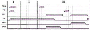
Fig. 4 shows a circuit diagram of the control circuit 40 of the image sensor according to fig. 2. A time switching sequence of the reset switch 26 (RES), the transfer gate 21 (TG), the selection switch 25 (SEL), the negative feedback switch 66 (FB), the signal value switch 71 (SHS), and the reference value switch 73 (SHR) is shown.
Before the exposure of the individual pixels 10 (period I to the left of the two vertical bars), the reset switch 26 (RES) is briefly closed and the transfer gate 21 (TG) is briefly opened to empty the photosensitive element 20, i.e. to remove charge carriers present therein. On one side of column amplifier 65, negative feedback switch 66 (FB) is closed. The exposure of the pixel 10 can now be performed (period II).
At the end of the exposure (time period III to the right of the two vertical bars), the readout process of the pixel 10 is initiated by briefly closing the reset switch 26 (RES) to remove charge formed by leakage current and/or scattered light from the readout node 22.
Selection switch 25 (SEL) and reference value switch 73 (SHR) are then closed so that the voltage signal of converter transistor 24 corresponding to the (residual) charge at sense node 22 reaches input capacitor 61 via column line 41. At the same time, the negative feedback switch 66 (FB) closed at the column amplifier 65 initially ensures that the column amplifier 65 operates in negative feedback mode and that the reference voltage VREF is applied to the negative input 67 of the column amplifier 65. The potential difference between the column line 41 and the negative input 67 of the column amplifier 65 causes the input capacitor 61 to charge accordingly. The negative feedback switch 66 (FB) is now open, causing the column amplifier 65 to enter the amplification mode. The now existing amplifier output signal is applied to the compensation line 42. The reference value capacitor 74 may be charged according to the amplifier output signal or the voltage at the amplifier output 69 by closing the reference value switch 73 (SHR). The reference value switch 73 (SHR) and the selection switch 25 (SEL) are then turned off. The reference value capacitor 74 may now or later be read.
Subsequently, the signal voltage value is read out. For this purpose the transfer gate 21 (TG) is briefly closed so that charge can move from the photosensitive element 20 to the read-out node 22. The selection switch 25 (SEL) and the signal value switch 71 (SHS) are then closed. Thereby changing the voltage at the input capacitor 61 and thereby changing the amplifier output signal that charges the signal value capacitor 72. While feedback back to sense node 22 occurs. For this purpose the amplifier output 69 of the column amplifier 65 whose amplifier output signal depends on the charge in the sense node 22 via the converter transistor 24, the column line 41 and the input capacitor 61 is fed back to the sense node 22 with a negative sign via the compensation line 42 and the feedback capacitor 28. In this reverse feedback operation, column amplifier 65 compensates for the voltage drop caused by the charge transfer at sense node 22 because column amplifier 65 increases the voltage at amplifier output 69 and thus at compensation line 42. Thereafter, the signal value switch 71 (SHS) and the selection switch 25 (SEL) are turned off. The signal value capacitor 72 may now or later be read. Based on the difference between the readout signal value and the reference value, an offset correction value corresponding to the exposure value of the pixel 10 can then be determined.
Claims (11)
1. An image sensor for an electronic camera, the image sensor comprising a plurality of pixels (10) for generating an exposure-related signal, wherein a respective one of the plurality of pixels (10) comprises at least:
-a photosensitive element (20) generating an electric charge from incident light;
-a read-out node (22);
-a transmission gate (21) selectively coupling the photosensitive element to the readout node (22);
-a converter transistor (24) converting the charge present at the sense node (22) into a voltage signal at a signal output (29); and
-a selection switch (25) connected to the signal output (29) of the converter transistor (24) to selectively couple the signal output (29) of the converter transistor (24) to a column line (41) of the image sensor associated with a plurality of pixels (10) of the image sensor;
wherein a column amplifier (65) is associated with a column line (41), wherein the column line (41) is coupled or couplable to a negative amplifier input (67) of the column amplifier (65) via an input capacitor (61), wherein the column amplifier (65) has an amplifier output (69) for outputting an amplifier output signal, wherein the amplifier output (69) is connected to a column readout circuit (70) and a compensation line (42), wherein the compensation line (42) is coupled to a respective readout node (22) of a pixel (10) associated with the column line (41) via a respective feedback capacitor (28).
2. The image sensor of claim 1, wherein the image sensor comprises a sensor array,
the column amplifier (65) is configured to generate the amplifier output signal from the voltage signal of the converter transistor (24) of the respective one of the pixels (10) received at the input capacitor (61) via the column line (41), and to output the amplifier output signal to the column readout circuit (70) and to the feedback capacitor (28) via the compensation line (42).
3. The image sensor of claim 2, wherein the image sensor further comprises a sensor element,
the column readout circuit (70) is configured to read out the amplifier output signal.
4. The image sensor of claim 1, wherein the image sensor comprises a sensor array,
the converter transistor (24), the column line (41), the input capacitor (61), the column amplifier (65), the compensation line (42) and the feedback capacitor (28) of the respective one of the pixels (10) form an inverse feedback loop for the readout node (22) of the respective one of the pixels (10).
5. The image sensor of claim 4, wherein the sensor further comprises a sensor element,
the input capacitor (61), the column amplifier (65) and the feedback capacitor (28) of the respective one of the pixels (10) are configured to keep the voltage at the readout node (22) of the respective one of the pixels (10) substantially constant.
6. The image sensor of claim 4, wherein the sensor further comprises a sensor element,
in case of an increase of charge at the readout node (22) of the respective one of the pixels (10), the input capacitor (61), the column amplifier (65) and the feedback capacitor (28) of the respective one of the pixels (10) are configured to increase the voltage at the compensation line (42) and thereby substantially compensate for the voltage variation at the readout node (22).
7. The image sensor of claim 1, wherein the image sensor comprises a sensor array,
the column amplifier (65) includes a positive amplifier input (68) to which a reference Voltage (VREF) is applied.
8. The image sensor of claim 7, wherein the image sensor further comprises a sensor element,
the negative amplifier input (67) is connectable to the amplifier output via a negative feedback switch (66),
by closing the negative feedback switch (66), the column amplifier (65) is able to enter a negative feedback mode in which a potential difference between the voltage at the column line (41) and the reference Voltage (VREF) is set at the input capacitor (61), and
by opening the negative feedback switch (66), the column amplifier (65) is able to enter an amplifying mode in which the amplifier output signal is representative of a potential difference at the input capacitor (61) that is changed relative to the negative feedback mode.
9. The image sensor of claim 8, wherein the image sensor further comprises a sensor element,
the image sensor has a control circuit (40), the control circuit (40) being configured to first put the column amplifier (65) into the negative feedback mode for reading out the respective one of the pixels (10); -subsequently bringing the column amplifier (65) into the amplifying mode; thereafter, the transfer gate (21) of the respective one of the pixels (10) is at least partially turned on for a short period of time to transfer charge to the readout node (22) of the respective one of the pixels (10); the column readout circuit (70) is then controlled to read out the signal values.
10. The image sensor of claim 9, wherein the image sensor further comprises a sensor element,
the respective one of the pixels (10) further has a reset switch (26), the reset switch (26) selectively coupling the readout node (22) to a reset potential (VDD),
-the control circuit (40) is configured to briefly close the reset switch (26) of the respective one of the pixels (10) to remove the charge present in the readout node (22) of the respective one of the pixels (10); then, in the amplifying mode of the column amplifier (65) and before the transfer gate (21) is turned on, the column readout circuit (70) is controlled to read out a reference value.
11. The image sensor of claim 1, wherein the image sensor comprises a sensor array,
the corresponding one pixel (10) further comprises:
-an overflow capacitor (30); and
-a further transmission gate (31) selectively coupling the read-out node (22) to the overflow capacitor (30).
Applications Claiming Priority (2)
| Application Number | Priority Date | Filing Date | Title |
|---|---|---|---|
| DE102021128022.2 | 2021-10-27 | ||
| DE102021128022.2A DE102021128022B3 (en) | 2021-10-27 | 2021-10-27 | image sensor |
Publications (1)
| Publication Number | Publication Date |
|---|---|
| CN116033276A true CN116033276A (en) | 2023-04-28 |
Family
ID=83689586
Family Applications (1)
| Application Number | Title | Priority Date | Filing Date |
|---|---|---|---|
| CN202211294721.9A Pending CN116033276A (en) | 2021-10-27 | 2022-10-21 | Image sensor |
Country Status (4)
| Country | Link |
|---|---|
| US (1) | US20230128595A1 (en) |
| EP (1) | EP4175312A1 (en) |
| CN (1) | CN116033276A (en) |
| DE (1) | DE102021128022B3 (en) |
Family Cites Families (8)
| Publication number | Priority date | Publication date | Assignee | Title |
|---|---|---|---|---|
| US6587142B1 (en) * | 1998-09-09 | 2003-07-01 | Pictos Technologies, Inc. | Low-noise active-pixel sensor for imaging arrays with high speed row reset |
| US9609243B2 (en) | 2007-05-25 | 2017-03-28 | Uti Limited Partnership | Systems and methods for providing low-noise readout of an optical sensor |
| US9094612B2 (en) | 2012-09-25 | 2015-07-28 | Semiconductor Components Industries, Llc | Back side illuminated global shutter image sensors with back side charge storage |
| US9041842B2 (en) * | 2013-07-12 | 2015-05-26 | Omnivision Technologies, Inc. | Image sensor pixel cell readout architecture |
| US9502457B2 (en) * | 2015-01-29 | 2016-11-22 | Semiconductor Components Industries, Llc | Global shutter image sensor pixels having centralized charge storage regions |
| JP6832649B2 (en) * | 2016-08-17 | 2021-02-24 | ブリルニクス インク | Solid-state image sensor, solid-state image sensor drive method, and electronic equipment |
| US10791292B1 (en) * | 2019-04-30 | 2020-09-29 | Semiconductor Components Industries, Llc | Image sensors having high dynamic range imaging pixels |
| US20200412980A1 (en) | 2019-06-28 | 2020-12-31 | Apple Inc. | Stacked Electromagnetic Radiation Sensors for Visible Image Sensing and Infrared Depth Sensing, or for Visible Image Sensing and Infrared Image Sensing |
-
2021
- 2021-10-27 DE DE102021128022.2A patent/DE102021128022B3/en active Active
-
2022
- 2022-10-10 EP EP22200623.1A patent/EP4175312A1/en active Pending
- 2022-10-21 CN CN202211294721.9A patent/CN116033276A/en active Pending
- 2022-10-26 US US17/973,707 patent/US20230128595A1/en active Pending
Also Published As
| Publication number | Publication date |
|---|---|
| US20230128595A1 (en) | 2023-04-27 |
| EP4175312A1 (en) | 2023-05-03 |
| DE102021128022B3 (en) | 2023-02-02 |
Similar Documents
| Publication | Publication Date | Title |
|---|---|---|
| US6320616B1 (en) | CMOS image sensor with reduced fixed pattern noise | |
| EP0986898B1 (en) | Cmos image sensor with improved fill factor | |
| US7345269B2 (en) | Method and apparatus providing configurable current source device for image sensors with a selective current at an output node | |
| EP1271930B1 (en) | Image sensing apparatus capable of outputting image with converted resolution, its control method, and image sensing system | |
| US6128039A (en) | Column amplifier for high fixed pattern noise reduction | |
| US5969758A (en) | DC offset and gain correction for CMOS image sensor | |
| JP4277339B2 (en) | Active pixel sensor readout channel | |
| US6963371B2 (en) | Image pickup apparatus including a plurality of pixels, each having a photoelectric conversion element and an amplifier whose output is prevented from falling below a predetermined level | |
| US6037577A (en) | Amplifying solid-state image pickup device and operating method of the same | |
| US8330843B2 (en) | Solid-state image sensing device, method for driving solid-state image sensing device, and image sensing system incorporated with solid-state image sensing device | |
| US8058928B2 (en) | Operational amplifier for an active pixel sensor | |
| US20020134918A1 (en) | Changeable gain amplifier, solid-state imaging device and optical signal reading method | |
| US7355645B2 (en) | Image pickup apparatus with potential fluctuation prevention | |
| EP0928103A2 (en) | CMOS imaging sensors | |
| US7427790B2 (en) | Image sensor with gain control | |
| US6822211B2 (en) | Solid-state image-sensing device | |
| US8026960B2 (en) | Image sensor and associated readout system | |
| JP2001177775A (en) | Solid-state image sensing device, image sensing system, and driving method for the device | |
| JP3890207B2 (en) | Imaging apparatus and imaging system | |
| US20020105012A1 (en) | Image sensor with correlated double sampling technique using switched-capacitor technology | |
| US20060027733A1 (en) | Apparatus and method of digital imaging on a semiconductor substrate | |
| US7872676B2 (en) | Methods, systems, and devices for offset compensation in CMOC imagers | |
| US8269870B2 (en) | Imaging device for suppressing variations in electric potentials | |
| CN116033276A (en) | Image sensor | |
| EP1220534A1 (en) | Image sensor with correlated double sampling technique using switched-capacitor technology |
Legal Events
| Date | Code | Title | Description |
|---|---|---|---|
| PB01 | Publication | ||
| PB01 | Publication |