CN1155152C - Amplifier - Google Patents
Amplifier Download PDFInfo
- Publication number
- CN1155152C CN1155152C CNB998010057A CN99801005A CN1155152C CN 1155152 C CN1155152 C CN 1155152C CN B998010057 A CNB998010057 A CN B998010057A CN 99801005 A CN99801005 A CN 99801005A CN 1155152 C CN1155152 C CN 1155152C
- Authority
- CN
- China
- Prior art keywords
- mentioned
- variable resistor
- effect transistor
- field
- resistance
- Prior art date
- Legal status (The legal status is an assumption and is not a legal conclusion. Google has not performed a legal analysis and makes no representation as to the accuracy of the status listed.)
- Expired - Fee Related
Links
Images


Classifications
-
- H—ELECTRICITY
- H03—ELECTRONIC CIRCUITRY
- H03G—CONTROL OF AMPLIFICATION
- H03G1/00—Details of arrangements for controlling amplification
- H03G1/0005—Circuits characterised by the type of controlling devices operated by a controlling current or voltage signal
- H03G1/0035—Circuits characterised by the type of controlling devices operated by a controlling current or voltage signal using continuously variable impedance elements
- H03G1/007—Circuits characterised by the type of controlling devices operated by a controlling current or voltage signal using continuously variable impedance elements using field-effect transistors [FET]
-
- H—ELECTRICITY
- H03—ELECTRONIC CIRCUITRY
- H03H—IMPEDANCE NETWORKS, e.g. RESONANT CIRCUITS; RESONATORS
- H03H11/00—Networks using active elements
- H03H11/02—Multiple-port networks
- H03H11/24—Frequency-independent attenuators
- H03H11/245—Frequency-independent attenuators using field-effect transistor
-
- H—ELECTRICITY
- H03—ELECTRONIC CIRCUITRY
- H03K—PULSE TECHNIQUE
- H03K2217/00—Indexing scheme related to electronic switching or gating, i.e. not by contact-making or -breaking covered by H03K17/00
- H03K2217/0054—Gating switches, e.g. pass gates
Landscapes
- Control Of Amplification And Gain Control (AREA)
- Amplifiers (AREA)
- Transmitters (AREA)
Abstract
在携带终端发送部的高频部中,为了在70dB以上的大范围内线性地(平直度±1dB)进行对一个控制电压的增益控制,用至少由两个以上的串联的可变电阻51、52构成的信号线51连接信号输入部34和信号输出部35,将并联连接的可变电阻53、54分别连接在信号输入部34和接地线57之间、以及信号输出部35和接地线57之间,将增益控制线56连接在可变电阻51、52、53、54上,将基准电压施加部23、27、31、33连接在各个可变电阻51、52、53、54上,将增益控制电压施加部19通过增益控制线56连接在各个可变电阻51、52、53、54上。
In the high-frequency section of the terminal transmitter, in order to linearly control the gain of a control voltage over a wide range of 70dB or more (flatness ±1dB), a signal line 51 consisting of at least two series-connected variable resistors 51 and 52 is used to connect the signal input section 34 and the signal output section 35. Variable resistors 53 and 54 connected in parallel are connected between the signal input section 34 and the ground line 57, and between the signal output section 35 and the ground line 57, respectively. A gain control line 56 is connected to the variable resistors 51, 52, 53, and 54. Reference voltage application units 23, 27, 31, and 33 are connected to each of the variable resistors 51, 52, 53, and 54. A gain control voltage application unit 19 is connected to each of the variable resistors 51, 52, 53, and 54 via the gain control line 56.
Description
技术领域technical field
本发明涉及放大高频信号、而且能利用控制电压改变增益的放大器,特别是涉及作为移动通信终端的发送部的高频部中使用的被集成电路化了的半导体装置的放大器。The present invention relates to an amplifier that amplifies a high-frequency signal and whose gain can be changed by a control voltage, and particularly relates to an amplifier of an integrated circuit semiconductor device used in a high-frequency portion of a transmission portion of a mobile communication terminal.
背景技术Background technique
最近,在移动通信领域中,作为存取手段,CDMA方式正成为国际标准之一。在这样的通信方式中,伴随携带终端和基站的距离的减小,相邻信道的干扰增大,因此误码率增大、通话质量下降成为大问题。Recently, in the field of mobile communication, the CDMA method is becoming one of the international standards as an access means. In such a communication system, as the distance between the mobile terminal and the base station decreases, the interference of adjacent channels increases, so that an increase in the bit error rate and a decrease in call quality become serious problems.
为了克服这样的问题,有必要调整与携带终端和基站的距离对应的输出信号。具体地说,需要根据基站负担的单元范围的大小,在携带终端发送部中需要进行增益控制幅度在70dB以上的大范围内的增益控制。而且,作为CDMA方式的特征,是在至基站的某一定的距离内进行精度极高的增益控制。因此,必须是平直度为±1dB的线性好的增益控制。In order to overcome such problems, it is necessary to adjust the output signal corresponding to the distance between the portable terminal and the base station. Specifically, depending on the size of the cell area that the base station bears, it is necessary to perform gain control in a wide range with a gain control width of 70 dB or more in the portable terminal transmission unit. Furthermore, as a feature of the CDMA system, extremely high-precision gain control is performed within a certain fixed distance from the base station. Therefore, it must be a linear good gain control with a flatness of ±1dB.
另外,在携带终端发送部中如果进行增益的衰减,则噪声指数劣化,所以在用载波信号电平低的500MHz左右以下的中频部在70dB以上的大范围内进行增益的衰减的情况下,难以识别载波信号电平及其以外的噪声信号电平,通话质量下降。因此为了解决这样的问题,需要用载波信号电平高的500MHz左右以上的高频部进行增益控制,该高频部能容易地识别载波信号电平及其以外的噪声信号电平。In addition, if the attenuation of the gain is performed in the portable terminal transmission section, the noise figure will deteriorate, so it is difficult to perform gain attenuation in a wide range of 70dB or more by using an intermediate frequency section below about 500MHz with a low carrier signal level. Identify the carrier signal level and the noise signal level beyond it, the call quality degrades. Therefore, in order to solve such a problem, it is necessary to perform gain control using a high-frequency section with a high carrier signal level of about 500 MHz or higher, which can easily distinguish between the carrier signal level and other noise signal levels.
为了在携带终端发送部中,在上述的增益控制幅度为70dB以上、平直度为±1dB的范围内进行线性好的增益控制,以往的方法是:单独地生产第一半导体装置和第二半导体装置这样两种进行增益控制的半导体装置,上述第一半导体装置在高频部中用大的增益变化点进行台阶式控制,上述第二半导体装置在中频部中用线性增益变化范围进行连续控制,用外部电路将上述第一半导体装置和第二半导体装置连接组合起来。在携带终端,利用内部安装了微机·逻辑部的单独的半导体装置进行这样的增益控制。In order to perform gain control with good linearity in the range of the above-mentioned gain control range of 70 dB or more and flatness of ±1 dB in the transmission part of the portable terminal, the conventional method is to separately produce the first semiconductor device and the second semiconductor device. There are two kinds of semiconductor devices for gain control, the above-mentioned first semiconductor device performs stepwise control with a large gain change point in the high frequency part, and the above-mentioned second semiconductor device performs continuous control with a linear gain change range in the intermediate frequency part, The above-mentioned first semiconductor device and the second semiconductor device are connected and combined by an external circuit. In a portable terminal, such gain control is performed by a separate semiconductor device in which a microcomputer and a logic unit are installed.
之所以进行两种增益控制,是因为难以用构成高频部的一个半导体装置在例如增益控制幅度为70dB以上、平直度为±1dB的大范围内进行具有良好的线性的增益控制。The reason for performing two kinds of gain control is that it is difficult to perform gain control with good linearity in a wide range with a gain control width of 70 dB or more and a flatness of ±1 dB with one semiconductor device constituting the high frequency section.
以下,说明在现有的移动通信终端发送部中进行增益控制的作为具有代表性的半导体装置的放大器。Hereinafter, an amplifier as a typical semiconductor device that performs gain control in a conventional mobile communication terminal transmission unit will be described.
图19是表示在现有的移动通信终端发送部的高频部中进行台阶式增益控制的放大器(半导体装置)的结构的电路图。利用这样的放大器,用大的增益变化点进行增益的台阶式控制。FIG. 19 is a circuit diagram showing the configuration of an amplifier (semiconductor device) that performs stepwise gain control in a high frequency section of a transmission section of a conventional mobile communication terminal. With such an amplifier, stepwise control of the gain is performed with a large gain change point.
如图19所示,该放大器有连接作为信号输入部的输入端子14和作为信号输出部的输出端子15的由串联的可变电阻71构成的信号线74,在输入端子14和接地线76之间、以及在输出端子15和接地线76之间分别连接着并联的可变电阻72、73。接地线76连接在作为基本电位部的地GND上。增益控制线75连接在可变电阻71、72、73上。在该放大器中,构成增益控制电压施加部的增益控制电压施加端子4通过增益控制线75分别连接在可变电阻71、72、73上。As shown in FIG. 19, this amplifier has a
上述的可变电阻71、72、73是分别将电阻7、5、13连接在场效应晶体管6、1、9的栅极上构成的。构成可变电阻71的场效应晶体管6的漏极连接在输入端子14上,源极连接在输出端子15上。另外,构成可变电阻72的场效应晶体管1的漏极通过电容器2连接在输入端子14上,源极通过电容器3及接地线76连接在地GND上。另外,构成可变电阻73的场效应晶体管9的漏极通过电容器10连接在输出端子15上,源极通过电容器11及接地线76连接在地GND上。The above-mentioned
另外,构成可变电阻71的场效应晶体管6的栅极通过电阻7及增益控制线75连接在增益控制电压施加端子4上,构成可变电阻72的场效应晶体管1的源极通过增益控制线75连接在增益控制电压施加端子4上,构成可变电阻73的场效应晶体管9的源极通过增益控制线75连接在增益控制电压施加端子4上。另外,从锂电池等供给的电源电压VDD(3V左右的电池电压)加在构成可变电阻71的场效应晶体管6的源极上,GND电位通过电阻5、13被供给分别构成可变电阻72、73的场效应晶体管1、9的栅极。In addition, the gate of the
这里,各电容器2、3、10、11具有阻止直流电压施加的作用,各电阻7、5、14具有阻止高频信号进入的作用。Here, each
另外,在该放大器中,以调整衰减量的形式进行增益的调整,图中省略了提高增益用的本来的放大功能部。只就图19所示的电路而言,具有衰减器的功能。In addition, in this amplifier, the gain is adjusted by adjusting the attenuation amount, and the original amplification function part for increasing the gain is omitted in the figure. Only the circuit shown in Fig. 19 has the function of an attenuator.
图20是表示在图19所示的放大器中,各场效应晶体管6、1、9的阈值电压Vth为-1.0V时的增益控制的形态的特性曲线图。图20(a)表示构成可变电阻71的场效应晶体管(串联FET)6的增益控制电压Vc-增益(衰减量)特性曲线。另外,图20(b)表示构成并联的可变电阻72、73的场效应晶体管(分流FET)1、9的增益控制电压Vc-增益(衰减量)特性曲线,实线是两个场效应晶体管的特性,虚线是一个场效应晶体管的特性。图20(c)表示将图20(a)、(b)所示的特性合成后的图19所示的放大器的增益控制电压Vc-增益(衰减量)特性曲线。FIG. 20 is a characteristic graph showing the form of gain control when the threshold voltage Vth of each
如上所述,在各场效应晶体管6、1、9的阈值电压Vth为-1.0V的情况下,就并联的可变电阻72、73的场效应晶体管1、9来说,在增益控制电压Vc为0.7V~1.0V的范围内,增益(衰减量)以46dB/V大小的斜率、在14dB的范围内,与增益控制电压Vc的变化成正比地变化,就串联的可变电阻71的场效应晶体管6来说,在增益控制电压Vc为2.0V~2.3V的范围内,增益(衰减量)以50dB/V大小的斜率、在15dB的范围内,与增益控制电压Vc的变化成正比地变化,在增益控制电压Vc为1.0V~2.0V的范围内,不进行增益控制,增益(衰减量)与增益控制电压Vc的变化无关而保持一定的值。就是说,不进行增益控制的增益控制电压区间ΔV的大小为1.0V。As described above, when the threshold voltage Vth of each of the
图21是表示在图19所示的放大器中,各场效应晶体管6、1、9的阈值电压Vth为-2.0V时的增益控制的形态的特性曲线图。图21(a)表示构成可变电阻71的场效应晶体管(串联FET)6的增益控制电压Vc-增益(衰减量)特性曲线。另外,图21(b)表示构成并联的可变电阻72、73的场效应晶体管(分流FET)1、9的增益控制电压Vc-增益(衰减量)特性曲线,实线是两个场效应晶体管的特性,虚线是一个场效应晶体管的特性。图21(a)、(b)与图20(a)、(b)相同。图21(c)表示将图21(a)、(b)所示的特性合成后的图19所示的放大器的增益控制电压Vc-增益(衰减量)特性曲线。FIG. 21 is a characteristic graph showing the form of gain control when the threshold voltage Vth of each
如上所述,在各场效应晶体管6、1、9的阈值电压Vth为-2.0V的情况下,就串联的可变电阻71的场效应晶体管6来说,在增益控制电压Vc为1.0V~1.3V的范围内,增益(衰减量)以50dB/V大小的斜率、在15dB的范围内,与增益控制电压Vc的变化成正比地变化,就并联的可变电阻72、73的场效应晶体管1、9来说,在增益控制电压Vc为1.7V~2.0V的范围内,增益(衰减量)以46dB/V大小的斜率、在14dB的范围内,与增益控制电压Vc的变化成正比地变化,在增益控制电压Vc为1.3V~1.7V的范围内,不进行增益控制,增益(衰减量)与增益控制电压Vc的变化无关而保持一定的值。就是说,不进行增益控制的增益控制电压区间ΔV的大小为0.4V。As described above, when the threshold voltage Vth of each
具有上述特性的放大器在进行台阶式控制的情况下,台阶式地切换增益控制电压Vc,每隔一定的值台阶式地切换增益(衰减量),与中频的连续增益控制相组合,在例如增益控制幅度为70dB以上的范围内实现线性(±1dB以下)的增益控制。In the case of the stepwise control of the amplifier with the above characteristics, the gain control voltage Vc is switched stepwise, and the gain (attenuation) is switched stepwise every certain value, combined with the continuous gain control of the intermediate frequency, for example, the gain Linear gain control (below ±1dB) is realized within the control range of 70dB or more.
图22表示用高频部进行增益控制的上述那种放大器的台阶式控制特性曲线图之一例。通常设定增益的台阶数为2~10个台阶左右,在图22中,将30dB的增益控制幅度从增益低的开始,按顺序每隔15dB设定成这样三个台阶:低、中、高各种方式。符号VCL、VCM、VCH是对应于各方式的增益控制电压,符号POUT表示输出信号的大小。另外,在图20、图21中,虽然增益控制幅度为29dB,但为了简化计算,进位成30dB后进行图示。Fig. 22 shows an example of a step control characteristic graph of the above-mentioned amplifier whose gain is controlled by a high-frequency section. Usually, the number of steps to set the gain is about 2 to 10 steps. In Figure 22, the gain control range of 30dB starts from the low gain, and is set to three steps every 15dB in order: low, medium and high. in various ways. The symbols V CL , V CM , and V CH are gain control voltages corresponding to each mode, and the symbol P OUT represents the magnitude of the output signal. In addition, in Fig. 20 and Fig. 21, although the gain control range is 29dB, in order to simplify the calculation, it is rounded up to 30dB for illustration.
另一方面,作为与进行图19所示的台阶式的增益控制的放大器(高频放大器)组合使用、用中频部连续地进行增益控制的放大器(中频放大器),虽然省略了具体的电路图,但主要是使用硅双极型晶体管。On the other hand, as an amplifier (intermediate frequency amplifier) that performs gain control continuously by an intermediate frequency part in combination with an amplifier (high frequency amplifier) that performs stepwise gain control shown in FIG. Mainly silicon bipolar transistors are used.
在使用双极型晶体管进行增益控制的放大器的情况下,根据其电路结构的特征,在信号电平小时,能进行范围较大、而且线性好的增益控制。因此,在用中频部进行增益控制的放大器中,利用增益呈线性变化的关系,进行连续控制。In the case of an amplifier using bipolar transistors for gain control, due to the characteristics of its circuit structure, gain control can be performed over a wide range and with good linearity when the signal level is small. Therefore, in an amplifier whose gain is controlled by an intermediate frequency section, continuous control is performed using a relationship in which the gain changes linearly.
图23是用中频部进行增益控制的放大器的连续控制特性曲线图。如图23所示,电平信号小时,能进行增益控制幅度为40dB、平直度为±1dB、范围较大、而且线性好的增益控制,对应于用高频部的台阶式控制的各种方式,用中频部进行连续控制。符号VCFINE是各方式时的微调增益控制电压,符号POUT表示输出信号的大小Fig. 23 is a graph showing continuous control characteristics of an amplifier whose gain is controlled by an intermediate frequency section. As shown in Figure 23, when the level signal is small, the gain control range is 40dB, the flatness is ±1dB, the range is large, and the linearity is good. Mode, use the intermediate frequency part for continuous control. The symbol V CFINE is the fine-tuning gain control voltage in each mode, and the symbol P OUT represents the size of the output signal
另外,图24是将台阶式控制和连续控制组合起来的移动通信终端发送部的增益控制特性曲线图。通过将图22中的台阶式控制的各种方式和图23中的连续控制分别组合起来,在移动通信终端发送部中能进行增益控制幅度为70dB、平直度为±1dB的范围较大、而且线性好的增益控制。In addition, FIG. 24 is a graph showing a gain control characteristic graph of a mobile communication terminal transmission unit in which step control and continuous control are combined. By combining the various modes of the step control in Fig. 22 and the continuous control in Fig. 23 respectively, the range of the gain control range of 70dB and the flatness of ±1dB is relatively large in the transmitting part of the mobile communication terminal, And good linear gain control.
如上所述,迄今在移动通信终端发送部中,为了进行增益控制幅度为70dB、平直度为±1dB的范围较大、而且线性好的增益控制,单独地生产用高频部进行台阶式控制的装置和用中频部进行连续控制的装置,再用外部电路将安装了这些半导体芯片的两种放大器(半导体装置)连接组合起来。As mentioned above, until now, in the transmission part of mobile communication terminals, in order to perform gain control with a wide gain control range of 70dB, a flatness of ±1dB, and good linearity, the high-frequency part for production alone has performed stepwise control. The device and the device for continuous control by the intermediate frequency part, and then use the external circuit to connect and combine the two types of amplifiers (semiconductor devices) on which these semiconductor chips are mounted.
而且,其理由是因为在上述现有的结构中,在输入端子14和输出端子15之间只连接一段由场效应晶体管6构成的串联的可变电阻71,在15~18dB左右大范围内不能取得对应于控制电压的增益控制量的直线部分,增益控制幅度也窄,为30dB,所以用一个放大器难以只用移动通信终端发送部的高频部进行增益控制幅度为70dB以上、平直度为±1dB的范围大、而且线性好的增益控制。Moreover, its reason is because in the above-mentioned existing structure, only a section of series-connected
可是,如上所述,在使两种独立的放大器(半导体装置)进行单独的增益控制的情况下,存在下述的问题。However, as described above, when two independent amplifiers (semiconductor devices) are individually controlled for gain, there are the following problems.
第一个问题是:如果将由高频部进行增益控制的放大器用于台阶式控制,则在串联的可变电阻71进行线性增益控制工作的增益控制电压范围和并联的可变电阻72、73进行线性增益控制工作的增益控制电压范围之间,存在不进行增益控制的非增益控制电压区间ΔV,所以在通过台阶式地切换增益控制电压Vc、台阶式地切换增益(衰减量)的情况下,即使对应于增益(衰减量),高精度地切换增益控制电压Vc,也难以进行高精度的增益控制。换句话说,为了高精度地切换增益(衰减量),存在增益控制电压Vc的选择变得复杂的问题。The first problem is: if the amplifier whose gain is controlled by the high-frequency part is used for step control, the gain control voltage range in which the
第二个问题是:如果并用单独的增益控制(台阶式控制、连续控制),即,如果用两种单独的放大器(半导体装置)进行单独的增益控制(台阶式控制、连续控制),则从图24中的增益控制特性曲线可知,在进行台阶式控制的各种方式的切换时,由于连续控制还同时变更增益控制电压Vc的设定,所以在方式切换的前后发生增益差异,不能实现所希望的平直特性,增益控制的高精度化变得困难了。另外,微机·逻辑部的控制电压必须设定成两种,变得复杂了。另外,存在移动通信终端的电路结构变得复杂、占用空间大的问题。The second problem is: if separate gain control (step control, continuous control) is used together, that is, if two separate amplifiers (semiconductor devices) are used for separate gain control (step control, continuous control), then from It can be seen from the gain control characteristic curve in Fig. 24 that when switching between various modes of step control, since continuous control also changes the setting of the gain control voltage Vc at the same time, there is a difference in gain before and after the mode switching, which cannot realize It becomes difficult to achieve the desired flat characteristic and high accuracy of gain control. In addition, the control voltage of the microcomputer and the logic part must be set to two types, which becomes complicated. In addition, there is a problem that the circuit configuration of the mobile communication terminal becomes complicated and occupies a large space.
发明内容Contents of the invention
本发明的第一个目的是提供一种在进行台阶式控制的情况下,能进行高精度的增益控制、或容易选择控制电压的放大器。A first object of the present invention is to provide an amplifier capable of high-accuracy gain control and easy selection of a control voltage when step control is performed.
本发明的第二个目的是提供一种能在大范围内线性地进行一种控制电压的增益控制的放大器。A second object of the present invention is to provide an amplifier capable of linearly performing a gain control of a control voltage over a wide range.
为了达到第一个目的,本发明的放大器备有:连接信号输入部和信号输出部的例如由场效应晶体管形成的可变电阻构成的信号线;分别连接在信号输入部与接地线之间、以及信号输出部与接地线之间的并联可变电阻;连接在各可变电阻上的增益控制线;连接在各可变电阻上的基准电压施加部;以及通过增益控制线连接在各可变电阻上的增益控制电压施加部。In order to achieve the first object, the amplifier of the present invention is equipped with: the signal line that connects the signal input part and the signal output part, for example, the variable resistance formed by the field effect transistor; And the parallel variable resistance between the signal output part and the ground wire; the gain control line connected to each variable resistance; the reference voltage application part connected to each variable resistance; and the gain control line connected to each variable resistance The gain on the resistor controls the voltage applying part.
如果采用该结构,则通过适当地设定供给各可变电阻的基准电压,供给串联的可变电阻和并联的可变电阻通用的增益控制电压,进行增益控制时,能缩小串联的可变电阻进行线性增益控制工作的增益控制电压范围和并联的可变电阻进行线性增益控制工作的增益控制电压范围之间的不进行增益控制的增益控制电压区间,在进行台阶式控制的情况下,能进行高精度的增益控制,另外容易选择控制电压。According to this structure, by appropriately setting the reference voltage supplied to each variable resistor, a common gain control voltage is supplied to the series variable resistors and the parallel connected variable resistors, and the gain control can reduce the size of the series variable resistors. The gain control voltage range without gain control between the gain control voltage range where the linear gain control works and the gain control voltage range where the parallel variable resistors perform linear gain control work can be controlled in the case of step control. High-precision gain control and easy selection of control voltage.
在构成上述串联的可变电阻及并联的可变电阻的场效应晶体管全部为单栅型的情况下,通过设定构成串联的可变电阻及并联的可变电阻的场效应晶体管的栅宽相等,能使串联的可变电阻及并联的可变电阻的增益控制特性相同。In the case where all the field effect transistors constituting the series variable resistors and the parallel variable resistors are single-gate type, by setting the gate widths of the field effect transistors constituting the series variable resistors and the parallel variable resistors to be equal, , so that the gain control characteristics of the variable resistors connected in series and the variable resistors connected in parallel are the same.
另外,如果使构成串联的可变电阻的场效应晶体管为多栅型的,则能增大增益控制宽度,同时能谋求低失真化。In addition, if the field effect transistors constituting the variable resistors connected in series are of a multi-gate type, the gain control width can be increased, and at the same time, low distortion can be achieved.
另外,如果使串联的可变电阻进行线性增益控制工作的增益控制电压范围和并联的可变电阻进行线性增益控制工作的增益控制电压范围之间的不进行增益控制的增益控制电压区间小于0.15V,则在进行台阶式控制的情况下,能进行高精度的增益控制,另外容易选择控制电压。In addition, if the gain control voltage range without gain control between the gain control voltage range in which the series variable resistors perform linear gain control operation and the gain control voltage range in which the parallel connection variable resistors perform linear gain control operation is less than 0.15V , then in the case of step control, high-precision gain control can be performed, and it is easy to select the control voltage.
另外,通过设定基准电压施加部加在并联的可变电阻上的电压值,以便在可变电阻进行线性增益控制工作的增益控制电压范围内,使并联的可变电阻进行线性增益控制工作的增益控制电压范围平滑地连续,在进行台阶式控制的情况下,能进行高精度的增益控制,或者容易选择控制电压。In addition, by setting the voltage value applied to the variable resistors connected in parallel by the reference voltage applying section, the variable resistors connected in parallel can perform the linear gain control operation within the gain control voltage range in which the variable resistors perform the linear gain control operation. The gain control voltage range is smooth and continuous, and in the case of step control, high-precision gain control can be performed, or the control voltage can be easily selected.
另外,公用的基准电压也可以通过电阻施加在并联的可变电阻的各个场效应晶体管的栅极上,在此情况下,能减少基准电压源的个数。In addition, the common reference voltage can also be applied to the gates of the field effect transistors of the variable resistors connected in parallel through resistors. In this case, the number of reference voltage sources can be reduced.
为了达到第二个目的,本发明的放大器是在上述放大器的结构中,使连接信号输入部和信号输出部的由例如场效应晶体管形成的可变电阻至少为两个以上的多级结构。有时将电容器插在构成多个串联的可变电阻的各场效应晶体管之间。In order to achieve the second object, the amplifier of the present invention has a multi-stage structure in which at least two variable resistors formed of, for example, field effect transistors connecting the signal input unit and the signal output unit are formed in the above amplifier structure. Capacitors are sometimes inserted between field effect transistors forming multiple series connected variable resistors.
如果采用该结构,则由于使多级连接的至少由两个以上的场效应晶体管构成的串联的可变电阻的工作只移动线性增益控制工作范围部分,分别补足串联的可变电阻的线性工作范围,只用一个增益控制电压进行各方式的切换,所以没有增益的差异,能以极高的精度对控制电压进行线性增益控制工作。If this structure is adopted, since the work of the series-connected variable resistors composed of at least two field effect transistors connected in multiple stages only moves the part of the linear gain control working range, the linear working ranges of the series-connected variable resistors are respectively complemented. , Only one gain control voltage is used to switch the various modes, so there is no difference in gain, and the linear gain control of the control voltage can be performed with extremely high precision.
使多级连接的至少由两个以上的场效应晶体管构成的串联的可变电阻的增益控制工作只移动线性增益控制工作范围部分,将不同的基准电压加在串联连接的至少两个以上的场效应晶体管的各源极上。在这样的结构中,由于用一个增益控制电压进行增益控制,所以能进行精度极高的增益控制。另外,可以自由地变更增益控制工作电压的设定。Make the gain control work of the series variable resistors composed of at least two field effect transistors connected in multiple stages only move the part of the linear gain control working range, and add different reference voltages to at least two field effect transistors connected in series Each source of the effect transistor. In such a configuration, since gain control is performed with one gain control voltage, extremely high-precision gain control can be performed. In addition, the setting of the gain control operating voltage can be freely changed.
作为另一种结构,是将不同的电压加在串联连接的至少两个以上的场效应晶体管的各栅极上。在这样的结构中,由于将相同的基准电压加在串联的可变电阻用的至少两个以上的场效应晶体管的各源极上,所以即使基准电压变化,也能进行精度良好的增益控制。另外,能自由地变更增益控制工作电压的设定。As another configuration, different voltages are applied to gates of at least two or more field effect transistors connected in series. In such a configuration, since the same reference voltage is applied to the respective sources of at least two field effect transistors connected in series for variable resistors, accurate gain control can be performed even if the reference voltage varies. In addition, the setting of the gain control operating voltage can be freely changed.
作为另一种结构,是采用使串联连接的至少两个以上的场效应晶体管具有不同的阈值电压的场效应晶体管的结构。在这样的结构中,由于用一个增益控制电压进行增益控制,所以能进行精度极高的增益控制。另外,由于将相同的基准电压加在串联的可变电阻用的至少两个以上的场效应晶体管的各源极上,所以即使基准电压变化,也能进行精度良好的增益控制。另外,由于能减少电压的施加,所以能简化电路结构。As another configuration, at least two field effect transistors connected in series have different threshold voltages. In such a configuration, since gain control is performed with one gain control voltage, extremely high-precision gain control can be performed. In addition, since the same reference voltage is applied to the respective sources of at least two or more field effect transistors connected in series for variable resistors, gain control with high precision can be performed even if the reference voltage varies. In addition, since the application of voltage can be reduced, the circuit configuration can be simplified.
在构成上述串联的可变电阻及并联的可变电阻的场效应晶体管全部为单栅型的情况下,通过设定构成串联的可变电阻及并联的可变电阻的场效应晶体管的栅宽相等,能使串联的可变电阻及并联的可变电阻的增益控制特性相同。In the case where all the field effect transistors constituting the series variable resistors and the parallel variable resistors are single-gate type, by setting the gate widths of the field effect transistors constituting the series variable resistors and the parallel variable resistors to be equal, , so that the gain control characteristics of the variable resistors connected in series and the variable resistors connected in parallel are the same.
另外,如果使构成串联的可变电阻的场效应晶体管为多栅型的,则能增大增益控制宽度,同时能谋求低失真化。In addition, if the field effect transistors constituting the variable resistors connected in series are of a multi-gate type, the gain control width can be increased, and at the same time, low distortion can be achieved.
另外,公用的基准电压也可以通过电阻施加在并联的可变电阻的各个场效应晶体管的栅极上,在此情况下,能减少基准电压源的个数。In addition, the common reference voltage can also be applied to the gates of the field effect transistors of the variable resistors connected in parallel through resistors. In this case, the number of reference voltage sources can be reduced.
另外,将与输入侧串联的可变电阻对应的基准电压施加部施加的电压设定得比与输出侧串联的可变电阻对应的基准电压施加部施加的电压高出相当于输出侧串联的可变电阻进行线性增益控制工作的增益控制电压范围的值,或者通过设定基准电压施加部加在并联的可变电阻上的电压值,以便在串联的可变电阻进行线性增益控制工作的增益控制电压范围内,使并联的可变电阻进行线性增益控制工作的增益控制电压范围平滑地连续,在进行连续控制的情况下,能进行高精度的增益控制。In addition, the voltage applied by the reference voltage application unit corresponding to the variable resistor connected in series on the input side is set to be higher than the voltage applied by the reference voltage application unit corresponding to the variable resistor connected in series on the output side by an amount equivalent to the available voltage on the output side. The value of the gain control voltage range for the linear gain control operation of the variable resistance, or the gain control of the linear gain control operation of the series variable resistance by setting the voltage value applied to the parallel variable resistance by the reference voltage applying part In the voltage range, the gain control voltage range in which the variable resistors connected in parallel perform linear gain control operation is smooth and continuous, and in the case of continuous control, high-precision gain control can be performed.
另外,通过设定与输入侧串联的可变电阻对应的基准电压施加部施加的电压比与输出侧串联的可变电阻对应的基准电压施加部施加的电压高,能将输入侧串联的可变电阻和输出侧串联的可变电阻两者并联的可变电阻的失真特性的各劣化点分散开,能使劣化的失真功率不重叠,能防止与并联的可变电阻的工作并用时失真特性的劣化。In addition, by setting the voltage applied by the reference voltage applying part corresponding to the variable resistor connected in series on the input side to be higher than the voltage applied by the reference voltage applying part corresponding to the variable resistor connected in series on the output side, the variable resistor connected in series on the input side can be connected The points of deterioration of the distortion characteristics of the variable resistors connected in parallel to the resistor and the variable resistors connected in series on the output side are dispersed, so that the deteriorated distortion power does not overlap, and it is possible to prevent the deterioration of the distortion characteristics when the variable resistors connected in parallel are used together. deteriorating.
以上,利用这些结构作为解决课题的手段。As described above, these configurations are used as means for solving the problems.
通过采用上述第一种结构,在移动通信终端发送部的高频部等中,将各个适当的基准电压供给串联的可变电阻和并联的可变电阻,能缩小或消除各可变电阻进行线性增益控制工作的增益控制电压范围之间的不进行增益控制的增益控制电压区间。其结果,进行增益的台阶式控制时,能高精度地进行增益控制。By adopting the above-mentioned first structure, in the high-frequency section of the mobile communication terminal transmission section, etc., each appropriate reference voltage is supplied to the variable resistors connected in series and the variable resistors connected in parallel, and the linearity of each variable resistor can be reduced or eliminated. The gain control voltage range in which the gain control is not performed between the gain control voltage ranges in which the gain control works. As a result, when the stepwise control of the gain is performed, the gain control can be performed with high precision.
通过采用上述第二种结构,在移动通信终端发送部的高频部等中,利用串联多级连接的至少由两个以上的场效应晶体管构成的可变电阻,增大信号输入部和信号输出部之间的串联电阻,而且,使多级连接的至少由两个以上的场效应晶体管构成的串联的可变电阻的工作只移动线性增益控制工作范围部分,以分别补足串联的可变电阻的线性工作范围,通过只用一个增益控制电压进行各方式的切换,以消除增益的差异,并能扩大控制电压的线性(平直度为±1dB左右)的增益控制范围。而且,能在大范围内高精度地进行增益控制工作。而且,通过增加串联的可变电阻的连接级数,能在70dB以上的大范围内以极高的精度进行控制电压的线性(平直度为±1dB左右)的增益控制工作。By adopting the above-mentioned second structure, in the high-frequency part of the mobile communication terminal transmission part, etc., the variable resistance composed of at least two or more field effect transistors connected in series and multi-stage is used to increase the signal input part and the signal output. The series resistance between the parts, and the work of the multi-stage connection of the series variable resistance composed of at least two field effect transistors only moves the part of the linear gain control working range to complement the series connection of the series variable resistance. Linear working range, by only using one gain control voltage to switch between various modes, to eliminate the difference in gain, and to expand the gain control range of the linearity of the control voltage (the flatness is about ±1dB). Furthermore, the gain control operation can be performed with high precision over a wide range. Moreover, by increasing the number of series connected variable resistors, gain control of the linearity of the control voltage (with a flatness of about ±1dB) can be performed with extremely high precision in a wide range above 70dB.
附图说明Description of drawings
图1是表示本发明的第一实施形态的放大器的结构框图。Fig. 1 is a block diagram showing the configuration of an amplifier according to a first embodiment of the present invention.
图2是表示本发明的第一实施形态的放大器的具体结构框图。Fig. 2 is a block diagram showing a specific configuration of the amplifier according to the first embodiment of the present invention.
图3是表示在图2所示的放大器中,在各场效应晶体管6、1、9的阈值电压Vth为-0.7V的情况下,将Vref11设定为1.8V、将Vref12、Vref13都设定为1.0V时的增益控制的形态的特性曲线图。FIG. 3 shows that in the amplifier shown in FIG. 2, when the threshold voltage Vth of each
图4是图2所示的放大器的增益控制电压的增益控制特性曲线图。FIG. 4 is a graph showing gain control characteristics of the gain control voltage of the amplifier shown in FIG. 2 .
图5是表示本发明的第二实施形态的放大器的具体结构框图。Fig. 5 is a block diagram showing a specific configuration of an amplifier according to a second embodiment of the present invention.
图6是表示在图5所示的放大器中,在各场效应晶体管6、1、9的阈值电压Vth为-0.7V的情况下,将Vref11设定为1.8V、将Vref12、Vref13都设定为1.0V时的增益控制的形态的特性曲线图。FIG. 6 shows that in the amplifier shown in FIG. 5, when the threshold voltage Vth of each
图7是表示本发明的第三实施形态的放大器的结构框图。Fig. 7 is a block diagram showing the configuration of an amplifier according to a third embodiment of the present invention.
图8是表示在本发明的第三实施形态中,为了能将不同的电压加在串联的可变电阻用的场效应晶体管21、25的各源极上,分别设置了基准电压施加端子23、27的放大器的具体结构的电路图。Fig. 8 shows that in the third embodiment of the present invention, in order to be able to apply different voltages to the source electrodes of the
图9是表示在图8所示的放大器中,在各场效应晶体管21、25、16、28的阈值电压Vth为-0.7V的情况下,将Vref1设定为1.9V、将Vref2设定为1.6V、将Vref3、Vref4都设定为1.1V时的增益控制的形态的特性曲线图。FIG. 9 shows that in the amplifier shown in FIG. 8, when the threshold voltage Vth of each
图10是本发明的第三实施形态的增益控制电压的增益控制特性曲线图。Fig. 10 is a graph showing the gain control characteristics of the gain control voltage according to the third embodiment of the present invention.
图11是本发明的第三实施形态的增益控制电压的900kHz失谐的相邻频道泄漏功率的特性曲线图。Fig. 11 is a characteristic graph of adjacent channel leakage power for 900 kHz detuning of the gain control voltage according to the third embodiment of the present invention.
图12是表示在本发明的第三实施形态中,为了能将基准电压加在各个可变电阻上,分别设置了偏压电阻38、39、40的放大器的具体结构的电路图。Fig. 12 is a circuit diagram showing a specific structure of an amplifier provided with bias resistors 38, 39, 40 in order to apply a reference voltage to each variable resistor in the third embodiment of the present invention.
图13是表示本发明的第四实施形态的放大器的结构框图。Fig. 13 is a block diagram showing the configuration of an amplifier according to a fourth embodiment of the present invention.
图14是表示在本发明的第四实施形态中,为了能将不同的电压加在串联的可变电阻用的场效应晶体管21、25的各栅极上,设置了增益控制电压施加端子42、19的放大器的具体结构的电路图。14 shows that in the fourth embodiment of the present invention, in order to be able to apply different voltages to the gates of the
图15是表示在本发明的第四实施形态中,为了能将不同的电压加在串联的可变电阻用的场效应晶体管21、25的各栅极上,设置了偏压电阻36、37,另外为了能将基准电压加在各个可变电阻上,分别设置了偏压电阻41、39、40的放大器的具体结构的电路图。Fig. 15 shows that in the fourth embodiment of the present invention, in order to be able to apply different voltages to the gates of the
图16是表示本发明的第五实施形态的放大器的结构框图。Fig. 16 is a block diagram showing the configuration of an amplifier according to a fifth embodiment of the present invention.
图17是表示在本发明的第五实施形态中,为了使串联的可变电阻用的场效应晶体管21、25在施加相同的基准电压及相同的增益控制电压后进行移动工作,将阈值电压分别不同的场效应晶体管21、25用于串联的可变电阻的放大器的具体结构的电路图。Fig. 17 shows that in the fifth embodiment of the present invention, in order to make the
图18是表示在本发明的第五实施形态中,为了能将基准电压加在各个可变电阻上,分别设置了偏压电阻41、39、40的放大器的具体结构的电路图。Fig. 18 is a circuit diagram showing a specific structure of an amplifier provided with
图19是表示现有例的放大器的结构的电路图。FIG. 19 is a circuit diagram showing the configuration of a conventional amplifier.
图20是表示在图19所示的放大器中,各场效应晶体管6、1、9的阀值电压Vth为-1.0V时的增益控制形态的特性曲线图。FIG. 20 is a characteristic graph showing the form of gain control when the threshold voltage Vth of each of the
图21是表示在图19所示的放大器中,各场效应晶体管6、1、9的阈值电压Vth为-2.0V时的增益控制形态的特性曲线图。FIG. 21 is a characteristic graph showing the form of gain control when the threshold voltage Vth of each of the
图22是现有的高频部中使用的放大器的增益控制电压的台阶式控制的特性曲线图。Fig. 22 is a characteristic graph of stepwise control of gain control voltage of an amplifier used in a conventional high frequency section.
图23是现有的中频部中使用的放大器的增益控制电压的连续控制的特性曲线图。Fig. 23 is a characteristic graph of continuous control of gain control voltage of an amplifier used in a conventional intermediate frequency section.
图24是现有的移动通信终端发送部中将两种放大器组合起来时的增益控制的特性曲线图。Fig. 24 is a characteristic graph of gain control when two types of amplifiers are combined in a transmission unit of a conventional mobile communication terminal.
具体实施方式Detailed ways
以下,参照附图说明本发明的第一实施形态。Hereinafter, a first embodiment of the present invention will be described with reference to the drawings.
图1是表示本发明的第一实施形态的放大器(半导体集成电路装置)的结构的简略框图,图2是表示本发明的第一实施形态的放大器的具体结构电路图。该放大器集成在一个半导体衬底(GaAs)上,在移动通信终端发送部中进行台阶式的增益控制。另外,这样的结构也可以集成在硅衬底上,特别是用硅构成时还能同时集成微机·逻辑部。1 is a schematic block diagram showing the configuration of an amplifier (semiconductor integrated circuit device) according to the first embodiment of the present invention, and FIG. 2 is a circuit diagram showing a specific configuration of the amplifier according to the first embodiment of the present invention. The amplifier is integrated on a semiconductor substrate (GaAs), and performs stepwise gain control in the transmission part of a mobile communication terminal. In addition, such a structure can also be integrated on a silicon substrate, and in particular, a microcomputer and a logic part can be integrated at the same time when it is formed of silicon.
利用这样的放大器,用增益变化大的点进行增益的台阶式控制,通过与中频部的进行连续的(线性的)增益控制的放大器组合起来使用,实现70dB以上的大范围的增益控制。Using such an amplifier, gain stepwise control is performed at a point where the gain changes greatly, and is used in combination with an amplifier that performs continuous (linear) gain control in the intermediate frequency section to achieve a wide range of gain control over 70dB.
如图1及图2所示,该放大器有连接作为信号输入部的输入端子14和作为信号输出部的输出端子15的由串联的可变电阻71构成的信号线74,在输入端子14和接地线76之间、以及在输出端子15和接地线76之间分别连接着并联的可变电阻72、73。接地线76连接在作为基本电位部的地GND上。增益控制线75连接在可变电阻71、72、73上。在该放大器中,构成基准电压施加部的基准电压施加端子8、12A、12B分别连接在可变电阻71、72、73上,基准电压Vref11、Vref12、Vref13被供给各个基准电压施加端子8、12A、12B。另外,构成增益控制电压施加部的增益控制电压施加端子4通过增益控制线75分别连接在各个可变电阻71、72、73上。另外,也可以将公用的基准电压供给并联的可变电阻72、73。这一点在以下的各实施形态中也一样。As shown in Fig. 1 and Fig. 2, this amplifier has the
上述的可变电阻71、72、73是分别将电阻7、5、13连接在场效应晶体管6、1、9的栅极上构成的。构成串联的可变电阻71的场效应晶体管6的漏极连接在输入端子14上,源极连接在输出端子15上。另外,构成输入侧的并联的可变电阻72的场效应晶体管1的漏极通过电容器2连接在输入端子14上,源极通过电容器3及接地线76连接在地GND上。另外,构成输出侧的并联的可变电阻73的场效应晶体管9的漏极通过电容器10连接在输出端子15上,源极通过电容器11及接地线76连接在地GND上。The above-mentioned
另外,构成可变电阻71的场效应晶体管6的栅极通过电阻7及增益控制线75连接在增益控制电压施加端子4上,构成可变电阻72的场效应晶体管1的源极通过增益控制线75连接在增益控制电压施加端子4上,构成可变电阻73的场效应晶体管9的源极通过增益控制线75连接在增益控制电压施加端子4上。In addition, the gate of the
另外,基准电压Vref11被从基准电压施加端子8加在构成可变电阻71的场效应晶体管6的源极上,基准电压Vref12、Vref13被从基准电压施加端子12A、12B分别通过电阻5、13加在分别构成可变电阻72、73的场效应晶体管1、9的栅极上。In addition, the reference voltage Vref11 is applied from the reference
这里,各电容器2、3、10、11具有阻止直流电压施加的作用,各电阻7、5、13具有阻止高频信号进入的作用。Here, each
由于上述电阻7、5、13阻止高频信号进入,所以如下所述设定下限值和上限值。首先,下限值为1kΩ。该设定理由是因为作为隔离,如果达不到20dB以上,高频信号就会进入,损失增大等,影响控制特性,如果设定为上述的值,则作为隔离,能获得20dB以上。Since the above-mentioned
另外,上限值为100kΩ。该设定理由是因为场效应晶体管的栅·漏电流例如流了1μA的情况下,且在插入场效应晶体管的栅极的电阻的阻值为100kΩ的情况下,该电阻上的电压降VDROP为In addition, the upper limit value is 100 kΩ. The reason for this setting is that when the gate/drain current of the field effect transistor flows, for example, 1 μA, and the resistance value of the resistor inserted into the gate of the field effect transistor is 100 kΩ, the voltage drop V DROP across the resistor is for
VDROP=1×10-6×100×103=0.1(V)V DROP =1×10 −6 ×100×10 3 =0.1(V)
如果电阻值超过100kΩ,则控制电压的偏移为0.1V,对增益控制特性的影响不能忽视。If the resistance value exceeds 100kΩ, the offset of the control voltage is 0.1V, and the influence on the gain control characteristics cannot be ignored.
另外,在该放大器中,以调整衰减量的形态进行增益的调整,图中省略了提高增益用的本来的放大功能部。就图2所示的电路而言,具有衰减器的功能。这一点在以下的各实施形态中也一样。In addition, in this amplifier, the gain adjustment is performed by adjusting the attenuation amount, and the original amplification function part for increasing the gain is omitted in the figure. As far as the circuit shown in Figure 2 is concerned, it has the function of an attenuator. This also applies to each of the following embodiments.
图3是表示在图2所示的放大器中,在各场效应晶体管6、1、9的阈值电压Vth为-0.7V的情况下,将Vref11设定为1.8V、将Vref12、Vref13都设定为1.0V时的增益控制的形态的特性曲线图。图3(a)表示构成串联的可变电阻71的场效应晶体管(串联FET)6的增益控制电压Vc-增益(衰减量)特性曲线。另外,图3(b)表示构成并联的可变电阻72、73的场效应晶体管(分流FET)1、9的增益控制电压Vc-增益(衰减量)特性曲线,实线是两个场效应晶体管的特性,虚线是一个场效应晶体管的特性。图3(c)表示将图3(a)、(b)所示的特性合成后的图2所示的放大器的增益控制电压Vc-增益(衰减量)特性曲线。FIG. 3 shows that in the amplifier shown in FIG. 2, when the threshold voltage Vth of each
如上所述,在各场效应晶体管6、1、9的阈值电压Vth为-0.7V的情况下,就串联的可变电阻71的场效应晶体管6来说,在增益控制电压Vc为1.1V~1.4V的范围内,增益(衰减量)以50dB/V大小的斜率、在15dB的范围内,与增益控制电压Vc的变化成正比地变化,就并联的可变电阻72、73的场效应晶体管1、9来说,在增益控制电压Vc为1.4V~1.7V的范围内,增益(衰减量)以46dB/V大小的斜率、在14dB的范围内,与增益控制电压Vc的变化成正比地变化,不进行增益控制的增益控制电压区间ΔV为0V。这时,增益控制幅度为:对串联的可变电阻71来说为15dB,对并联的可变电阻72、73来说为14dB,所以合计为29dB。As mentioned above, when the threshold voltage Vth of each
图4是用图2所示的移动通信终端发送部的高频部进行增益控制的第二实施形态的放大器的增益控制电压Vc的增益控制特性曲线图。FIG. 4 is a graph showing gain control characteristics of the gain control voltage Vc of the amplifier of the second embodiment in which the gain control is performed by the high frequency unit of the transmission unit of the mobile communication terminal shown in FIG. 2 .
说明如上构成的放大器的工作情况。在携带终端中利用锂电池等,用3.0V左右的电压进行驱动。另外,场效应晶体管的阈值电压表示可变电阻开始进行增益控制工作的偏压,串联的可变电阻71及并联的可变电阻72、73用的场效应晶体管6、1、9的阈值电压全都相等。在该例中为-0.7V。上述的基准电压Vref11、Vref12、Vref13分别加在串联的可变电阻71的基准电压施加端子8和并联的可变电阻72、73的基准电压施加端子12A、12B上。The operation of the amplifier constructed as above will be described. A lithium battery or the like is used in a portable terminal, and it is driven at a voltage of about 3.0V. In addition, the threshold voltage of the field effect transistor indicates the bias voltage at which the variable resistor starts gain control operation, and the threshold voltages of the
这里,由场效应晶体管形成的可变电阻在栅·源间电压VGS比场效应晶体管的阈值电压Vth小(VGS≤Vth)时,呈完全阻断状态,电阻值达到最大。另外,各场效应晶体管形成的栅·源间电压VGS用栅极电压VG和源极电压VS的差(VG-VS)表示,用增益控制电压Vc和基准电压Vref11、Vref12、Vref13的组合改变电阻值。因此,如果改变基准电压Vref11、Vref12、Vref13的设定值,能控制可变电阻所能进行增益控制的增益控制电压Vc的范围。Here, when the gate-source voltage VGS of the field effect transistor is smaller than the threshold voltage Vth of the field effect transistor (VGS≤Vth), the variable resistance formed by the field effect transistor is completely blocked, and the resistance value reaches the maximum value. In addition, the gate-source voltage VGS formed by each field effect transistor is represented by the difference (VG-VS) between the gate voltage VG and the source voltage VS, and the resistance is changed by the combination of the gain control voltage Vc and the reference voltages Vref11, Vref12, and Vref13. value. Therefore, if the set values of the reference voltages Vref11, Vref12, and Vref13 are changed, the range of the gain control voltage Vc within which the variable resistor can perform gain control can be controlled.
因此,通过适当地设定串联的可变电阻71的基准电压Vref11和并联的可变电阻72、73的基准电压Vref12、Vref13,能在串联的可变电阻72的增益控制工作范围和并联的可变电阻72、73的增益控制工作范围之间,使不进行增益控制的增益控制电压区间ΔV为小于0.15V的值。串联的可变电阻71和并联的可变电阻72、73分别对增益控制电压Vc分担的增益控制范围,虽然在图3中串联的可变电阻71在低压侧,并联的可变电阻72、73在高压侧,但反过来也可以。Therefore, by appropriately setting the reference voltage Vref11 of the
现在,说明增益控制电压区间ΔV在0.15V以上不适合的理由。通常,多半采用5级左右的台阶式控制,每一级控制7~8dB,斜率约为50dB/V,所以控制电压被设定为台阶式的0.15V。因此,如果不进行增益控制的增益控制电压区间ΔV在0.15V以上,则即使改变控制电压,也会产生增益不变化的点,所以不能高精度地进行增益控制。Now, the reason why the gain control voltage interval ΔV is not suitable for 0.15V or more will be described. Usually, about 5 levels of step control are mostly used, each level controls 7~8dB, and the slope is about 50dB/V, so the control voltage is set to a step type of 0.15V. Therefore, if the gain control voltage range ΔV in which gain control is not performed is 0.15 V or more, there will be a point where the gain does not change even if the control voltage is changed, so that gain control cannot be performed with high accuracy.
另外,不进行增益控制的增益控制电压区间ΔV的下限值为0V。另外,即使各控制特性重叠也基本上没有问题。但是,由于重叠的部分的斜率变陡,所以在进行上述的5级控制的情况下,需要变更控制电压的设定。In addition, the lower limit value of the gain control voltage section ΔV in which the gain control is not performed is 0V. In addition, there is basically no problem even if the respective control characteristics overlap. However, since the slope of the overlapping portion becomes steeper, it is necessary to change the setting of the control voltage when performing the above-mentioned five-level control.
如上所述,通过使不进行增益控制的增益控制电压区间ΔV为小于0.15V的值,能使串联的可变电阻71的增益控制范围和并联的可变电阻72、73的增益控制范围平滑地连续地连接,进行台阶式控制时,能进行高精度的增益控制,而且容易选择增益控制电压Vc。As described above, by setting the gain control voltage interval ΔV in which gain control is not performed to a value smaller than 0.15V, the gain control range of the
在作为增益控制电压Vc而将0~1.1V的电压加在增益控制电压施加端子4上的情况下(图4:增益控制电压范围(a)),串联的可变电阻71的电阻值RON(T-FET)表现为最大值,并联的可变电阻72、73的电阻值RON(S-FET)表现为最小值,所以从输入端子14输入的信号衰减、不增大增益,来自输出端子15的输出信号的大小POUT达到最小。When a voltage of 0 to 1.1V is applied to the gain control
在将超过1.1V的电压加在增益控制电压施加端子4上的情况下(图4:增益控制电压范围(b)),并联的可变电阻72、73的电阻值RON(S-FET)仍表现为最小值,而串联的可变电阻71的电阻值RON(T-FET)开始减小,所以输出信号的大小POUT增大。通常,由场效应晶体管构成的可变电阻进行线性增益控制工作的增益控制电压范围为0.2~0.3V左右,直到1.4V的电压加在增益控制电压施加端子4上之前,增益呈线性地增大15dB。When a voltage exceeding 1.1V is applied to the gain control voltage application terminal 4 (FIG. 4: Gain control voltage range (b)), the resistance value R ON (S-FET) of the
如果1.4V的电压加在增益控制电压施加端子4上(图4:增益控制电压范围(c)),则减小了的串联的可变电阻71的电阻值RON(T-FET)表现为最小值,已经表现为最小值的并联的可变电阻72、73的电阻值RON(S-FET)开始增大,所以输出信号的大小POUT增大。直到1.7V的电压加在增益控制电压施加端子4上之前,增益按照与增益控制电压为1.1~1.4V的范围(b)不同的灵敏度呈线性地增大14(=2×7)dB。If a voltage of 1.4V is applied to the gain control voltage application terminal 4 (Fig. 4: Gain control voltage range (c)), the reduced resistance value R ON (T-FET) of the
在将1.7V的电压加在增益控制电压施加端子4上的情况下(图4:增益控制电压范围(d)),串联的可变电阻71的电阻值RON(T-FET)仍表现为最小值,而并联的可变电阻72、73的电阻值RON(S-FET)表现为最大值,所以输出信号的大小POUT变为最大。在此时刻,该放大器所具有的增益控制幅度为29dB。即使将1.7V以上的电压加在增益控制电压施加端子4上,仍然是串联的可变电阻71的电阻值RON(T-FET)表现为最小值,并联的可变电阻72、73的电阻值RON(S-FET)表现为最大值,所以输出信号的大小POUT仍为最大。In the case where a voltage of 1.7V is applied to the gain control voltage application terminal 4 (Fig. 4: Gain control voltage range (d)), the resistance value R ON (T-FET) of the
具有上述特性的放大器进行台阶式控制时,台阶式地切换增益控制电压Vc,每隔一定的值台阶式地切换增益(衰减量),与中频的连续增益控制相组合,在增益控制幅度为70dB以上的范围内实现线性(±1dB以下)的增益控制。When the amplifier with the above characteristics is controlled stepwise, the gain control voltage Vc is switched stepwise, and the gain (attenuation) is switched stepwise every certain value, combined with the continuous gain control of the intermediate frequency, the gain control range is 70dB Linear (±1dB or less) gain control is realized within the above range.
如果采用该实施形态,则通过将适当的基准电压Vref11、Vref12、Vref13供给串联的可变电阻71和并联的可变电阻72、73,能使各可变电阻71、72、73进行线性增益控制工作的增益控制电压范围之间的不进行增益控制的增益控制电压区间减小、或者消除,所以进行增益的台阶式控制时,能高精度地进行增益控制。According to this embodiment, by supplying appropriate reference voltages Vref11, Vref12, and Vref13 to the
另外,在上述实施形态中,构成各可变电阻71、72、73的场效应晶体管6、1、9为单栅型,但采用其栅宽Wg相同者(当然栅长也相同),也能使可变电阻71的增益控制特性和两个可变电阻72、73的增益控制特性一致,也能使合成特性的线性好。In addition, in the above-mentioned embodiment, the
以下,参照附图说明本发明的第二实施形态。Hereinafter, a second embodiment of the present invention will be described with reference to the drawings.
图5是表示本发明的第二实施形态的放大器的具体结构框图。该放大器采用多栅(多个控制电极)型、在本例中为双栅型的场效应晶体管6A,代替图2中的单栅型的场效应晶体管6,通过电阻7A、7B和增益控制线75将场效应晶体管6A的各栅极连接在增益控制电压施加端子4上,其他结构与图2中的放大器相同。Fig. 5 is a block diagram showing a specific configuration of an amplifier according to a second embodiment of the present invention. The amplifier adopts a multi-gate (multiple control electrodes) type, in this example a double-gate field effect transistor 6A, instead of a single-gate
图6是表示在图5所示的放大器中,在各场效应晶体管6、1、9的阈值电压Vth为-0.7V的情况下,将Vref11设定为1.8V、将Vref12、Vref13都设定为1.0V时的增益控制的形态的特性曲线图。图6(a)表示构成串联的可变电阻71的场效应晶体管(串联FET)6的增益控制电压Vc-增益(衰减量)特性曲线。另外,图6(b)表示构成并联的可变电阻72、73的场效应晶体管(并联FET)1、9的增益控制电压Vc-增益(衰减量)特性曲线,实线是两个场效应晶体管的特性,虚线是一个场效应晶体管的特性。图6(c)表示将图6(a)、(b)所示的特性合成后的图6所示的放大器的增益控制电压Vc-增益(衰减量)特性曲线。FIG. 6 shows that in the amplifier shown in FIG. 5, when the threshold voltage Vth of each
如上所述,在各场效应晶体管6、1、9的阈值电压Vth为-0.7V的情况下,就串联的可变电阻71的场效应晶体管6来说,在增益控制电压Vc为1.1V~1.4V的范围内,增益(衰减量)以60dB/V大小的斜率、在18dB的范围内,与增益控制电压Vc的变化成正比地变化,就并联的可变电阻72、73的场效应晶体管1、9来说,在增益控制电压Vc为1.4V~1.7V的范围内,增益(衰减量)以46dB/V大小的斜率、在14dB的范围内,与增益控制电压Vc的变化成正比地变化,不进行增益控制的增益控制电压区间ΔV为0V。这时,增益控制幅度为:对串联的可变电阻71来说为18dB,对并联的可变电阻72、73来说为14dB,所以合计为32dB。As mentioned above, when the threshold voltage Vth of each
如果采用该实施形态,则由于作为构成可变电阻71的场效应晶体管6A采用双栅型的晶体管,所以增益控制幅度扩大3dB左右,失真特性能改善3dBc左右。如上所述,由于作为构成可变电阻71的场效应晶体管6A采用多栅型的场效应晶体管,所以能谋求扩大增益控制幅度和低失真化。其他效果与使用单栅型的场效应晶体管6的放大器相同。According to this embodiment, since a double-gate transistor is used as the field effect transistor 6A constituting the
以下,参照附图说明本发明的第三实施形态。Hereinafter, a third embodiment of the present invention will be described with reference to the drawings.
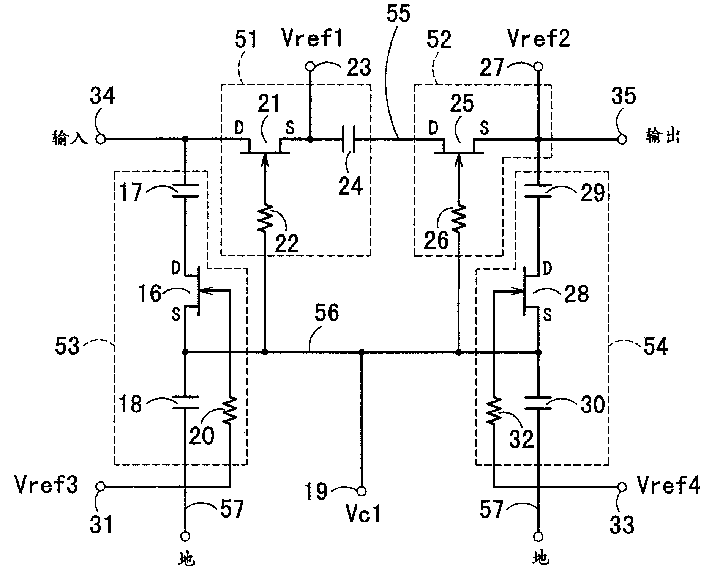
图7是表示本发明的第三实施形态的放大器(半导体集成电路装置)的结构的简略框图,图8是表示本发明的第三实施形态的具体结构的电路图。该放大器集成在一个半导体衬底(GaAs)上。另外,这样的结构也可以集成在硅衬底上,特别是用硅构成时还能同时集成微机·逻辑部。7 is a schematic block diagram showing the structure of an amplifier (semiconductor integrated circuit device) according to a third embodiment of the present invention, and FIG. 8 is a circuit diagram showing a specific structure of the third embodiment of the present invention. The amplifier is integrated on a semiconductor substrate (GaAs). In addition, such a structure can also be integrated on a silicon substrate, and in particular, a microcomputer and a logic part can be integrated at the same time when it is formed of silicon.
利用这样的放大器,用增益呈线性变化的区域进行增益的连续控制,与串联的可变电阻为一个的情况相比,能在大范围内实现线性好的增益控制。其结果,即使不与中频部的放大器的增益控制组合,也能单独地在大范围内实现线性好的增益控制。通过增多串联的可变电阻的个数,能在70dB以上的大范围内实现线性好的增益控制。With such an amplifier, continuous gain control is performed in a region where the gain changes linearly, and gain control with good linearity can be realized over a wide range compared with the case where only one variable resistor is connected in series. As a result, gain control with good linearity can be realized independently over a wide range without being combined with the gain control of the amplifier of the intermediate frequency section. By increasing the number of variable resistors connected in series, the gain control with good linearity can be realized in a large range above 70dB.
如图7及图8所示,该放大器有连接作为信号输入部的输入端子34和作为信号输出部的输出端子35的至少由两个以上串联的可变电阻51、52构成的信号线55,在输入端子34和接地线57之间、以及在输出端子35和接地线57之间分别连接着并联的可变电阻53、54。接地线57连接在作为基本电位部的地GND上。增益控制线56连接在可变电阻51、52、53、54上。在该放大器中,构成基准电压施加部的基准电压施加端子23、27、31、33分别连接在可变电阻51、52、53、54上,基准电压Vref1、Vref2、Vref3、Vref4被供给各个基准电压施加端子23、27、31、33。另外,构成增益控制电压施加部的增益控制电压施加端子19通过增益控制线56分别连接在各个可变电阻51、52、53、54上。另外,也可以将公用的基准电压供给并联的可变电阻53、54。这一点在以下的各实施形态中也一样。As shown in Fig. 7 and Fig. 8, this amplifier has the
上述的可变电阻51、52、53、54是分别将电阻22、26、20、32至少连接在场效应晶体管21、25、16、28的栅极上构成的。构成输入侧的串联的可变电阻51的场效应晶体管21的漏极连接在输入端子34上,源极连接在电容器24的一端上。构成输出侧的串联的可变电阻52的场效应晶体管25的漏极连接在电容器24的另一端上,源极连接在输出端子35上。另外,构成输入侧的并联的可变电阻53的场效应晶体管16的漏极通过电容器17连接在输入端子34上,源极通过电容器18及接地线57连接在地GND上。另外,构成输出侧的并联的可变电阻54的场效应晶体管28的漏极通过电容器29连接在输出端子35上,源极通过电容器30及接地线57连接在地GND上。The above
另外,构成可变电阻51的场效应晶体管21的栅极通过电阻22及增益控制线56连接在增益控制电压施加端子19上,构成可变电阻52的场效应晶体管25的栅极通过电阻26及增益控制线56连接在增益控制电压施加端子19上,构成可变电阻53的场效应晶体管16的源极通过增益控制线56连接在增益控制电压施加端子19上,构成可变电阻54的场效应晶体管28的源极通过增益控制线56连接在增益控制电压施加端子19上。In addition, the gate of the
另外,基准电压Vref1、Vref2被从基准电压施加端子23、27加在构成可变电阻51、52的场效应晶体管21、25的源极上,基准电压Vref3、Vref4被从基准电压施加端子31、33分别通过电阻20、32加在分别构成可变电阻53、54的场效应晶体管16、28的栅极上。In addition, the reference voltages Vref1 and Vref2 are applied from the reference
这里,各电容器17、18、24、29、30具有阻止直流电压施加的作用,各电阻20、22、26、32具有阻止高频信号进入的作用。Here, each
由于上述电阻20、22、26、32阻止高频信号进入,所以如下所述设定下限值和上限值。首先,下限值为1kΩ。该设定理由是因为作为隔离,如果达不到20dB以上,高频信号就会进入,损失增大等,影响控制特性,如果设定为上述的值,则作为隔离,能获得20dB以上。Since the above-mentioned
另外,上限值为100kΩ。该设定理由是因为场效应晶体管的栅·漏电流例如流了1μA的情况下,且在插入场效应晶体管的栅极的电阻的阻值为100kΩ的情况下,该电阻上的电压降VDROP为In addition, the upper limit value is 100 kΩ. The reason for this setting is that when the gate/drain current of the field effect transistor flows, for example, 1 μA, and the resistance value of the resistor inserted into the gate of the field effect transistor is 100 kΩ, the voltage drop V DROP across the resistor is for
VDROP=1×10-6×100×103=0.1(V)V DROP =1×10 −6 ×100×10 3 =0.1(V)
如果电阻值超过100kΩ,则控制电压的偏移为0.1V,对增益控制特性的影响不能忽视。If the resistance value exceeds 100kΩ, the offset of the control voltage is 0.1V, and the influence on the gain control characteristics cannot be ignored.
另外,在该放大器中,以调整衰减量的形态进行增益的调整,图中省略了提高增益用的本来的放大功能部。就图8所示的电路而言,具有衰减器的功能。这一点在以下的各实施形态中也一样。In addition, in this amplifier, the gain adjustment is performed by adjusting the attenuation amount, and the original amplification function part for increasing the gain is omitted in the figure. As far as the circuit shown in FIG. 8 is concerned, it has the function of an attenuator. This also applies to each of the following embodiments.
图9是表示在图8所示的放大器中,在各场效应晶体管21、25、16、28的阈值电压Vth为-0.7V的情况下,将Vref1设定为1.9V、将Vref2设定为1.6V、将Vref3、Vref4都设定为1.1V时的增益控制的形态的特性曲线图。图9(a)表示构成串联的可变电阻52的场效应晶体管(串联FET)25的增益控制电压Vc1-增益(衰减量)特性曲线。另外,图9(b)表示构成串联的可变电阻51的场效应晶体管(串联FET)21的增益控制电压Vc1-增益(衰减量)特性曲线。另外,图9(c)表示构成并联的可变电阻53、54的场效应晶体管(分流FET)16、28的增益控制电压Vc1-增益(衰减量)特性曲线,实线是两个场效应晶体管的特性,虚线是一个场效应晶体管的特性。图9(d)表示将图9(a)、(b)、(c)所示的特性合成后的图8所示的放大器的增益控制电压Vc1-增益(衰减量)特性曲线。FIG. 9 shows that in the amplifier shown in FIG. 8, when the threshold voltage Vth of each
如上所述,在各场效应晶体管21、25、16、28的阈值电压Vth为-0.7V的情况下,就串联的可变电阻52的场效应晶体管25来说,在增益控制电压Vc1为0.9V~1.2V的范围内,增益(衰减量)以50dB/V大小的斜率、在15dB的范围内,与增益控制电压Vc1的变化成正比地变化,就串联的可变电阻51的场效应晶体管21来说,在增益控制电压Vc1为1.2V~1.5V的范围内,增益(衰减量)以50dB/V大小的斜率、在15dB的范围内,与增益控制电压Vc1的变化成正比地变化,就并联的可变电阻53、54的场效应晶体管16、28来说,在增益控制电压Vc1为1.5V~1.8V的范围内,增益(衰减量)46dB/V大小的斜率、在14dB的范围内,与增益控制电压Vc1的变化成正比地变化,不进行增益控制的增益控制电压区间实际上没有。这时,增益控制幅度为:对串联的可变电阻51来说为15dB,对串联的可变电阻52来说为15dB,对并联的可变电阻53、54来说为14dB,所以合计为44dB,与串联的可变电阻为一个的情况相比,能获得可变幅度大的增益控制特性,通过增多串联的可变电阻的个数,还能进行70dB以上的范围内的增益控制。As described above, when the threshold voltage Vth of each of the
图10是用图8所示的移动通信终端发送部的高频部进行增益控制的第三实施形态的放大器的增益控制电压Vc1的增益控制特性曲线图。FIG. 10 is a graph showing the gain control characteristics of the gain control voltage Vc1 of the amplifier according to the third embodiment in which the gain control is performed by the high frequency part of the transmission part of the mobile communication terminal shown in FIG. 8. FIG.
说明如上构成的放大器的工作情况。在携带终端中利用锂电池等,用3.0V左右的电压进行驱动。另外,场效应晶体管的阈值电压表示可变电阻开始进行增益控制工作的偏压,串联的可变电阻51、52及并联的可变电阻53、54用的场效应晶体管的阈值电压全都相等。在该例中为-0.7V。The operation of the amplifier constructed as above will be described. A lithium battery or the like is used in a portable terminal, and it is driven at a voltage of about 3.0V. In addition, the threshold voltage of the field effect transistor indicates the bias voltage at which the variable resistors start gain control operation, and the threshold voltages of the field effect transistors for the series
上述的基准电压Vref1、Vref2分别加在串联的可变电阻51、52的基准电压施加端子23、27上,另外相同的基准电压Vref3、Vref4加在并联的可变电阻53、54的基准电压施加端子31、33上。加在串联的可变电阻51、52的基准电压施加端子23、27上的基准电压Vref1、Vref2两者中的加在输入侧的基准电压施加端子23上的基准电压Vref1比加在输出侧的基准电压施加端子27上的基准电压Vref2高出相当于进行线性增益控制工作的增益控制电压范围(0.2~0.3V)的大小。The above-mentioned reference voltages Vref1 and Vref2 are respectively applied to the reference
上述的基准电压Vref1、Vref2、Vref3、Vref4被设定成实际上看起来由串联的可变电阻51、52、53、54决定的线性增益控制工作范围呈连续的状态即可。在以下的实施形态中也一样。The above-mentioned reference voltages Vref1, Vref2, Vref3, and Vref4 are set so that the linear gain control operating range determined by the series
这里,由场效应晶体管形成的可变电阻在栅·源间电压VGS比场效应晶体管的阈值电压Vth小(VGS≤Vth)时,呈完全阻断状态,电阻值达到最大。另外,各场效应晶体管形成的栅·源间电压VGS用栅极电压VG和源极电压VS的差(VG-VS)表示,用增益控制电压Vc1和基准电压Vref1、Vref2、Vref3、Vref4的组合改变电阻值。因此,如果改变基准电压Vref1、Vref2、Vref3、Vref4的设定值,则能控制可变电阻所能进行增益控制的增益控制电压Vc1的范围。Here, when the gate-source voltage VGS of the field effect transistor is smaller than the threshold voltage Vth of the field effect transistor (VGS≤Vth), the variable resistance formed by the field effect transistor is completely blocked, and the resistance value reaches the maximum value. In addition, the gate-source voltage VGS formed by each field effect transistor is represented by the difference (VG-VS) between the gate voltage VG and the source voltage VS, and is represented by a combination of the gain control voltage Vc1 and the reference voltages Vref1, Vref2, Vref3, and Vref4 Change the resistor value. Therefore, if the set values of the reference voltages Vref1, Vref2, Vref3, and Vref4 are changed, the range of the gain control voltage Vc1 within which the variable resistor can perform gain control can be controlled.
因此,通过适当地分别设定串联的可变电阻51、52的基准电压Vref1、Vref2和并联的可变电阻53、54的基准电压Vref3、Vref4,能在串联的可变电阻51、52的增益控制工作范围和并联的可变电阻53、54的增益控制工作范围之间,使不进行增益控制的增益控制电压区间为小于0.15V的值。串联的可变电阻51、52和并联的可变电阻53、54分别对增益控制电压Vc1分担的增益控制范围,虽然在图9中串联的可变电阻52在低压侧,串联的可变电阻51在中压侧,并联的可变电阻53、54在高压侧,但也可以将该顺序反过来,可以任意地设定。Therefore, by appropriately setting the reference voltages Vref1, Vref2 of the
现在,说明增益控制电压区间ΔV在0.15V以上不适合的理由。通常,多半采用5级左右的台阶式控制,每一级控制7~8dB,斜率约为50dB/V,所以控制电压被设定为台阶式的0.15V。因此,如果不进行增益控制的增益控制电压区间ΔV在0.15V以上,则即使改变控制电压,也会产生增益不变化的点,所以不能高精度地进行增益控制。Now, the reason why the gain control voltage interval ΔV is not suitable for 0.15V or more will be described. Usually, about 5 levels of step control are mostly used, each level controls 7~8dB, and the slope is about 50dB/V, so the control voltage is set to a step type of 0.15V. Therefore, if the gain control voltage range ΔV in which gain control is not performed is 0.15 V or more, there will be a point where the gain does not change even if the control voltage is changed, so that gain control cannot be performed with high accuracy.
另外,不进行增益控制的增益控制电压区间ΔV的下限值为0V。另外,即使各控制特性重叠也基本上没有问题。但是,由于重叠的部分的斜率变陡,所以在进行上述的5级控制的情况下,需要变更控制电压的设定。In addition, the lower limit value of the gain control voltage section ΔV in which the gain control is not performed is 0V. In addition, there is basically no problem even if the respective control characteristics overlap. However, since the slope of the overlapping portion becomes steeper, it is necessary to change the setting of the control voltage when performing the above-mentioned five-level control.
如上所述,在进行增益的连续控制的情况下,通过分别适当的设定串联的可变电阻51的基准电压Vref1、串联的可变电阻52的基准电压Vref2、并联的可变电阻53、54的基准电压Vref3、Vref4,能使串联的可变电阻51、52和并联的可变电阻53、54的增益控制工作范围平滑地连续地连接起来,能用一个增益控制电压在大范围内进行线性好的增益控制。其结果,容易做到增益控制的高精度化,而且能简化电路结构、节省空间。As mentioned above, in the case of continuous gain control, by appropriately setting the reference voltage Vref1 of the
这里,假定场效应晶体管的阈值电压Vth都为-0.7V,则能将基准电压Vref1设定为1.9V,基准电压Vref2设定为1.6V,基准电压Vref3、Vref4都设定为1.1V。Here, assuming that the threshold voltage Vth of the field effect transistors is -0.7V, the reference voltage Vref1 can be set to 1.9V, the reference voltage Vref2 can be set to 1.6V, and the reference voltages Vref3 and Vref4 can both be set to 1.1V.
在将0~0.9V的电压加在增益控制电压施加端子19上的情况下(图10:增益控制电压范围(a)),串联的可变电阻51、52的电阻值RON(T-FET21)、RON(T-FET25)表现为最大值,并联的可变电阻53、54的电阻值RON(S-FET16、28)表现为最小值,所以从输入端子34输入的信号衰减、不增大增益,输出端子35上的输出信号的大小POUT达到最小。When a voltage of 0-0.9V is applied to the gain control voltage application terminal 19 (Fig. 10: gain control voltage range (a)), the resistance value R ON of the
在将超过0.9V的电压加在增益控制电压施加端子19上的情况下(图10:增益控制电压范围(b)),并联的可变电阻53、54的电阻值RON(S-FET 16、28)仍表现为最小值,输入侧的串联的可变电阻51的电阻值RON(T-FET21)仍表现为最大值,输出侧的串联的可变电阻52的电阻值RON(T-FET215)开始减小,所以输出信号的大小POUT增大。通常,由场效应晶体管构成的可变电阻进行线性增益控制工作的增益控制电压范围为0.2~0.3V左右,直到1.2V的电压加在增益控制电压施加端子19上之前,增益呈线性地增大15dB。When a voltage exceeding 0.9V is applied to the gain control voltage application terminal 19 (FIG. 10: gain control voltage range (b)), the resistance value R ON of the
如果1.2V的电压加在增益控制电压施加端子19上(图10:增益控制电压范围(c)),则减小了的输出侧的串联的可变电阻52的电阻值RON(T-FET25)表现为最小值,已经表现为最大值的输入侧的串联的可变电阻51的电阻值RON(T-FET21)开始减小,所以使灵敏度相同后,输出信号的大小POUT增大。这里,并联的可变电阻53、54的电阻值RON(S-FET16、28)表现为最小值。If a voltage of 1.2V is applied to the gain control voltage application terminal 19 (Fig. 10: gain control voltage range (c)), the resistance value R ON of the
如果1.5V的电压加在增益控制电压施加端子19上(图10:增益控制电压范围(d)),则减小了的输入侧的串联的可变电阻51的电阻值RON(T-FET21)与输出侧的串联的可变电阻52的电阻值RON(T-FET 25)一样,表现为最小值,已经表现为最小值的并联的可变电阻53、54的电阻值RON(S-FET16、28)开始增加,所以输出信号的大小POUT以与0.9~1.5V电压范围不同的灵敏度呈线性地增大14dB。If a voltage of 1.5V is applied to the gain control voltage applying terminal 19 (Fig. 10: gain control voltage range (d)), the resistance value R ON of the
在将1.8V的电压加在增益控制电压施加端子19上的情况下(图10:增益控制电压范围(e)),则串联的可变电阻51、52的电阻值RON(T-FET21)、RON(T-FET25)仍表现为最小值,由于并联的可变电阻53、54的电阻值RON(S-FET 16、28)表现为最大值,所以输出信号的大小POUT变为最大。在该时刻,该放大器所具有的增益控制幅度变为44dB。即使将1.8V的电压加在增益控制电压施加端子19上,由于串联的可变电阻51、52的电阻值RON(T-FET21)、RON(T-FET25)表现为最小值,并联的可变电阻53、54的电阻值RON(S-FET16、28)表现为最大值,所以输出信号的大小POUT仍为最大。In the case where a voltage of 1.8V is applied to the gain control voltage application terminal 19 (Fig. 10: gain control voltage range (e)), the resistance value R ON of the
如上所述,如果采用本实施形态,则由于通过电容器24将场效应晶体管构成的串联的可变电阻51、52连接成多级,使串联的可变电阻51、52的工作只移动线性增益控制工作范围部分,能分别补足串联的可变电阻51、52的线性工作范围,所以能在大范围内使对控制电压的增益控制量呈线性。通过从外部微机调整基准电压,能只在该串联的可变电阻51、52的线性增益控制工作范围内移动。As mentioned above, according to this embodiment, since the series
另外,在CDMA方式中,将符号附加在各信号上,在同一时间、用同一频率处理它们,所以设备的失真特性极其重要。特别是如本实施形态所述,只在由场效应晶体管构成的串联的可变电阻51、52的线性增益控制工作范围内的移动工作中,通过使输出侧的串联的可变电阻52比输入侧的串联的可变电阻51先对增益控制电压Vc1进行工作,能将输入侧串联的可变电阻51和输出侧串联的可变电阻52及并联的可变电阻53、54的失真特性的各劣化点分散开,能使劣化的失真功率不重叠,所以能防止与并联的可变电阻的工作并用时失真特性的劣化。如图11所示,与采用同样的结构而使串联的可变电阻51、52同时工作的情况相比,通过在900kHz失谐时的相邻频道泄漏功率(ACP900kHz)能进行失真特性约为4dBc左右的低失真工作。In addition, in the CDMA system, symbols are added to each signal, and they are processed at the same time and at the same frequency, so the distortion characteristics of the equipment are extremely important. In particular, as described in this embodiment, only in the moving operation within the linear gain control range of the series
另外,在上述实施形态中,在由场效应晶体管构成的串联的可变电阻51、52的移动工作中,虽然使输出侧的串联的可变电阻52比输入侧的串联的可变电阻51先对增益控制电压Vc1进行工作,但即使相反地使输入侧的串联的可变电阻51先工作,也能获得同样的特性。从而能增大微机·逻辑部的控制电压的设定自由度。In addition, in the above-mentioned embodiment, in the movement operation of the series
另外,在上述实施形态中,分别设置了输入侧的串联的可变电阻51的基准电压施加端子23、输出侧的串联的可变电阻52的基准电压施加端子27、以及并联的可变电阻53、54的基准电压施加端子31、33,但如图12所示,也可以利用偏压电阻38、39、40施加基准电压。这时,由于只用一个基准电压施加端子,所以能简化电路。偏压电阻38、39、40分别具有阻止高频信号进入的作用。电阻39被插入连接在上述可变电阻52的上述场效应晶体管25的源极和通过上述电阻20、32连接在上述可变电阻53、54的各个上述场效应晶体管16、28的栅极上的部分61之间,为了阻止高频信号进入,上述的偏压电阻38、39、40被设定为5kΩ以上、100kΩ以下的电阻值。In addition, in the above-mentioned embodiment, the reference
以下说明偏压电阻38、39、40被设定为5kΩ以上、100kΩ以下的电阻值的理由。The reason why the bias resistors 38 , 39 , and 40 are set to a resistance value of not less than 5 kΩ and not more than 100 kΩ will be described below.
首先,下限值为5kΩ左右的理由如下。偏压电阻38和场效应晶体管25并联连接,能用场效应晶体管25的可变电阻值进行增益控制。现在,在偏压电阻38比5kΩ小的情况下,即使增大场效应晶体管25的电阻值,作为偏压电阻38和场效应晶体管25的并联电路两端之间的电阻,为5kΩ左右,不会比它大,所以增益控制幅度变小,不能高精度地进行增益控制。就是说,不能阻止高频信号进入。另外,如果偏压电阻39、40的阻值也小,则由于高频信号通地,所以需要5kΩ以上(隔离为40dB以上)。另外,基准电压Vref1为3V时,流过各偏压电阻38、39、40的电流为First, the reason why the lower limit is about 5 kΩ is as follows. The bias resistor 38 is connected in parallel with the
I=3V/15kΩ=200μA以上I=3V/15kΩ=200μA or more
功率消耗增大。Power consumption increases.
另一方面,上限值为100kΩ的理由如下。基准电压Vref1为3V时,流过各偏压电阻38、39、40的电流为On the other hand, the reason why the upper limit is 100 kΩ is as follows. When the reference voltage Vref1 is 3V, the current flowing through each bias resistor 38, 39, 40 is
I=3V/300kΩ=10μAI=3V/300kΩ=10μA
现在,偏压电阻38两端的电压为Now, the voltage across the bias resistor 38 is
V=10μA×100kΩ=1VV=10μA×100kΩ=1V
这时,如果场效应晶体管的漏电流为1μA,则产生1μA×100kΩ=0.1V的偏压变化,致使增益控制特性偏移,不能精确地进行增益控制。At this time, if the leakage current of the field effect transistor is 1μA, a bias voltage change of 1μA×100kΩ=0.1V will be generated, causing the gain control characteristic to deviate, and the gain control cannot be performed accurately.
另外,在上述第三实施形态中,为了能将不同的电压加在串联的可变电阻51、52用的场效应晶体管的各源极上,分别安装了基准电压施加端子23、27,但也可以代之以如下的方法,如图13及图14所示,为了能将线性增益控制工作范围不同的增益控制电压Vc1、Vc2加在串联的可变电阻51、52用的场效应晶体管的各栅极上,也可以分别设置增益控制电压施加部42、19(第四实施形态)。另外,在图13中,58是第一增益控制线,59是第二增益控制线。In addition, in the above-mentioned third embodiment, in order to apply different voltages to the sources of the field effect transistors for the series
在此情况下,由增益控制电压施加部19将线性增益控制工作范围内电压差大的增益控制电压压Vc1、Vc2加在增益控制电压施加部42即可,不需要象以往使用多个个别的增益控制装置时那样设定复杂的电压。另外,由于将相同的基准电压Vref1加在串联的可变电阻51、52用的场效应晶体管21、25的各源极上,所以即使对应于基准电压Vref1的变化,也能精确地进行线性增益控制。连接在基准电压施加端子23和串联的可变电阻51、52用的场效应晶体管21、25的各源极之间的电阻41具有阻止高频信号的作用,被设定为5kΩ以上、100kΩ以下的电阻值。In this case, the gain control voltages Vc1 and Vc2 with a large voltage difference within the linear gain control operating range can be applied to the gain control
以下说明将电阻41设定为5kΩ以上、100kΩ以下的电阻值的理由。The reason why the
首先,下限值为5kΩ左右的理由如下。电阻41和场效应晶体管25并联连接,能用场效应晶体管25的可变电阻值进行增益控制。现在,在电阻41比5kΩ小的情况下,即使增大场效应晶体管25的电阻值,作为电阻41和场效应晶体管25的并联电路两端之间的电阻,为5kΩ左右,不会比它大,所以增益控制幅度变小,不能高精度地进行增益控制。就是说,不能阻止高频信号进入。First, the reason why the lower limit is about 5 kΩ is as follows. The
另一方面,上限值为100kΩ的理由如下。在流过场效应晶体管的漏电流的情况下(1μA左右),电阻41两端的电位差超过On the other hand, the reason why the upper limit is 100 kΩ is as follows. In the case of a leakage current (about 1 μA) flowing through the field effect transistor, the potential difference across the
V=1μA×100kΩ=0.1VV=1μA×100kΩ=0.1V
偏压发生变化,不能精确地进行增益控制。The bias voltage changes and gain control cannot be performed precisely.
同样如图15所示,为了能将线性增益控制工作范围不同的电压加在串联的可变电阻51、52用的场效应晶体管21、25的各栅极上,也可以分别设置电阻36、37。这时,由于只使用一个增益控制电压Vc1,所以能简化微机·逻辑部的设定,另外由于将相同的基准电压加在串联的可变电阻51、52用的场效应晶体管21、25的各源极上,所以即使对应于基准电压的变化,也能精确地进行线性增益控制。另外,关于基准电压,也可以用偏压电阻41、39、40进行基准电压的施加。在此情况下,由于只使用一个基准电压施加端子,所以能简化电路。偏压电阻41、39、40分别起着阻止高频信号进入的作用。为了阻止高频信号进入,上述的偏压电阻41、39、40被设定为5kΩ以上、100kΩ以下。如上设定电阻值范围的理由,与有关图12的说明相同。Also as shown in Figure 15, in order to add voltages with different linear gain control ranges to the gates of the
另外同样在上述第三实施形态中,为了能将不同的电压加在串联的可变电阻51、52用的场效应晶体管的各源极上,分别安装了基准电压施加端子23、27,但也可以采用如下的方法,如图16或图17所示,将相同的基准电压及相同的增益控制电压加在串联的可变电阻51、52用的场效应晶体管上,利用相当于使各场效应晶体管21、25进行线性增益控制工作的增益控制电压范围、而阈值电压不同的场效应晶体管进行移动工作(第五实施形态)。在此情况下,制作工序数增多,而其反面,呈图16及图17所示的电路结构,能减少电压施加端子,能进行简化。另外,由于将相同的基准电压加在串联的可变电阻51、52用的场效应晶体管21、25的各源极上,所以即使对应于基准电压的变化,也能精确地进行线性增益控制。连接在基准电压施加端子23和串联的可变电阻51、52用的场效应晶体管21、25的各源极之间的电阻41分别具有阻止高频信号进入的作用。In addition, in the above-mentioned third embodiment, in order to apply different voltages to the respective sources of the field effect transistors used for the series
另外,如图18所示,关于基准电压,也可以用偏压电阻41、39、40进行基准电压的施加。在此情况下,由于只使用一个基准电压施加端子,所以还能简化电路。偏压电阻41、39、40分别起着基准电压的偏压电阻及阻止高频信号进入的作用。In addition, as shown in FIG. 18 , as for the reference voltage, the
另外,在上述实施形态中,虽然采用了将由场效应晶体管构成的输入侧的串联的可变电阻51和输出侧的串联的可变电阻52这两个可变电阻进行多级连接的结构,但也可以多级连接更多的可变电阻,串联多级连接的可变电阻数越多,能分别涉足串联的可变电阻的线性工作范围,所以能扩大控制电压的线性信号控制范围。In addition, in the above-mentioned embodiment, although the configuration in which two variable resistors, the input-side
另外,在上述实施形态中,在各可变电阻51、52、53、54用的各场效应晶体管21、25、16、28的漏-源电极之间不进行任何并联连接,但为了控制各场效应晶体管21、25、16、28的固有电阻值的离散、以及控制可变电阻范围,也可以将并联电阻等连接在场效应晶体管21、25、16、28的漏-源电极之间使用。因此各可变电阻所具有的增益控制量稳定,能进行精度极高的增益控制。In addition, in the above-mentioned embodiment, no parallel connection is made between the drain-source electrodes of the respective
另外,在上述实施形态中,虽然各可变电阻51、52、53、54用的各场效应晶体管21、25、16、28的栅极的条数分别用一条构成,但也可以使用一条以上的多条栅极(多栅型),所使用的栅极的条数越多,增益越高,另外即使是高频输入信号,也能进行能抑制失真特性劣化的增益控制。In addition, in the above-mentioned embodiment, although the number of gates of each
另外,在构成可变电阻51、52、53、54的场效应晶体管21、25、16、28全部为单栅型的情况下,各场效应晶体管21、25、16、28的栅宽虽然不需要设定得相同,但在相同的情况下,能使两个并联的可变电阻53、54的合成增益控制特性和串联的可变电阻51、52的各增益控制特性一致,能使增益控制的线性极好。In addition, when the
另外,在上述实施形态中,虽然示出了将各场效应晶体管21、25、16、28用于各可变电阻51、52、53、54的情况,但本发明不限于此,例如也可以是二极管等。In addition, in the above-mentioned embodiment, although the case where each
另外,如果采用有两个以上串联的可变电阻的第三实施形态以后的各实施形态的放大器之类的电路结构,则不仅能进行增益的连续控制,而且能进行增益的台阶式控制,在此情况下,如第一或第二实施形态所示,能与中频部分的连续控制组合。如果这样处理,则与第一或第二实施形态相比,台阶式控制的增益范围广,结果能进一步扩大总体的增益控制范围。In addition, if a circuit structure such as the amplifier of each embodiment after the third embodiment with two or more variable resistors connected in series is adopted, not only the continuous control of the gain but also the stepwise control of the gain can be performed. In this case, as shown in the first or second embodiment, it can be combined with the continuous control of the intermediate frequency section. In this way, the gain range of the step control is wider than that of the first or second embodiment, and as a result, the overall gain control range can be further expanded.
另外,这些放大器不只是CDMA方式,而且可以用于各种移动体通信方式(PDG、GSM、PCS、Wideband-CDMA、DCS、PHS等)。In addition, these amplifiers can be used not only in the CDMA system but also in various mobile communication systems (PDG, GSM, PCS, Wideband-CDMA, DCS, PHS, etc.).
Claims (39)
Applications Claiming Priority (2)
| Application Number | Priority Date | Filing Date | Title |
|---|---|---|---|
| JP11562198 | 1998-04-24 | ||
| JP115621/1998 | 1998-04-24 |
Publications (2)
| Publication Number | Publication Date |
|---|---|
| CN1272977A CN1272977A (en) | 2000-11-08 |
| CN1155152C true CN1155152C (en) | 2004-06-23 |
Family
ID=14667196
Family Applications (1)
| Application Number | Title | Priority Date | Filing Date |
|---|---|---|---|
| CNB998010057A Expired - Fee Related CN1155152C (en) | 1998-04-24 | 1999-04-19 | Amplifier |
Country Status (5)
| Country | Link |
|---|---|
| US (1) | US6229370B1 (en) |
| EP (1) | EP0993111B1 (en) |
| CN (1) | CN1155152C (en) |
| DE (1) | DE69939359D1 (en) |
| WO (1) | WO1999056389A1 (en) |
Families Citing this family (17)
| Publication number | Priority date | Publication date | Assignee | Title |
|---|---|---|---|---|
| JP3605314B2 (en) * | 1999-05-31 | 2004-12-22 | 松下電器産業株式会社 | Mobile phone terminal |
| JP3332082B2 (en) | 2000-01-17 | 2002-10-07 | 日本電気株式会社 | High frequency variable attenuation circuit |
| US6762735B2 (en) * | 2000-05-12 | 2004-07-13 | Semiconductor Energy Laboratory Co., Ltd. | Electro luminescence display device and method of testing the same |
| US6657469B1 (en) * | 2002-05-23 | 2003-12-02 | Yazaki North America, Inc. | Multi-slew-rate switching circuit |
| AU2003244130A1 (en) * | 2002-06-20 | 2004-03-11 | Matsushita Electric Industrial Co., Ltd. | Switch device |
| JP3902111B2 (en) * | 2002-10-21 | 2007-04-04 | 新日本無線株式会社 | Switch semiconductor integrated circuit |
| US7250804B2 (en) * | 2002-12-17 | 2007-07-31 | M/A -Com, Inc. | Series/shunt switch and method of control |
| JP3934067B2 (en) * | 2003-02-06 | 2007-06-20 | 松下電器産業株式会社 | Attenuator switch and mobile phone terminal device using the same |
| JP4050246B2 (en) | 2003-07-01 | 2008-02-20 | 松下電器産業株式会社 | Attenuator and mobile phone terminal using the same |
| JP3839421B2 (en) * | 2003-07-03 | 2006-11-01 | 松下電器産業株式会社 | High frequency amplifier circuit and mobile communication terminal using the same |
| JP4246622B2 (en) * | 2003-12-26 | 2009-04-02 | 古野電気株式会社 | Microwave frequency converter |
| US7340229B2 (en) * | 2004-08-20 | 2008-03-04 | Matsushita Electric Industrial Co., Ltd. | High frequency amplification circuit and mobile communication terminal using the same |
| FR2884079B1 (en) * | 2005-03-31 | 2007-09-07 | Valeo Equip Electr Moteur | CONTROLLING A MOS TRANSISTOR |
| JP4998460B2 (en) * | 2006-03-10 | 2012-08-15 | 富士通株式会社 | Low noise amplifier |
| JP5035341B2 (en) * | 2007-07-30 | 2012-09-26 | 富士通株式会社 | Amplifier circuit |
| US8390359B2 (en) * | 2009-12-28 | 2013-03-05 | Maxim Integrated Products, Inc. | Low distortion MOS attenuator |
| US20160248400A1 (en) * | 2015-02-25 | 2016-08-25 | Analog Devices, Inc. | Apparatus and methods for radio frequency switching |
Family Cites Families (9)
| Publication number | Priority date | Publication date | Assignee | Title |
|---|---|---|---|---|
| FR2558023A1 (en) | 1984-01-10 | 1985-07-12 | Thomson Csf | CONTROLABLE IMPEDANCE CELL AND CIRCUIT FOR CONTROLLING THE CELL |
| US4890077A (en) | 1989-03-28 | 1989-12-26 | Teledyne Mec | FET monolithic microwave integrated circuit variable attenuator |
| US5281928A (en) * | 1992-10-26 | 1994-01-25 | M/A-Com, Inc. | Electronic attenuator |
| US5345123A (en) * | 1993-07-07 | 1994-09-06 | Motorola, Inc. | Attenuator circuit operating with single point control |
| JPH07273598A (en) | 1994-03-29 | 1995-10-20 | Nec Eng Ltd | Variable attenuator |
| JPH09252234A (en) | 1996-03-15 | 1997-09-22 | Toshiba Microelectron Corp | Semiconductor integrated circuit |
| US5666089A (en) * | 1996-04-12 | 1997-09-09 | Hewlett-Packard Company | Monolithic step attenuator having internal frequency compensation |
| US5767721A (en) | 1996-06-06 | 1998-06-16 | Itt Industries, Inc. | Switch circuit for FET devices having negative threshold voltages which utilize a positive voltage only |
| US6069503A (en) * | 1998-03-11 | 2000-05-30 | Intel Corporation | High value FET resistors on a submicron MOS technology |
-
1999
- 1999-04-19 CN CNB998010057A patent/CN1155152C/en not_active Expired - Fee Related
- 1999-04-19 WO PCT/JP1999/002085 patent/WO1999056389A1/en not_active Ceased
- 1999-04-19 EP EP99913721A patent/EP0993111B1/en not_active Expired - Lifetime
- 1999-04-19 DE DE69939359T patent/DE69939359D1/en not_active Expired - Lifetime
- 1999-04-19 US US09/446,626 patent/US6229370B1/en not_active Expired - Fee Related
Also Published As
| Publication number | Publication date |
|---|---|
| WO1999056389A1 (en) | 1999-11-04 |
| DE69939359D1 (en) | 2008-10-02 |
| US6229370B1 (en) | 2001-05-08 |
| EP0993111A4 (en) | 2005-05-11 |
| EP0993111A1 (en) | 2000-04-12 |
| EP0993111B1 (en) | 2008-08-20 |
| CN1272977A (en) | 2000-11-08 |
Similar Documents
| Publication | Publication Date | Title |
|---|---|---|
| CN1155152C (en) | Amplifier | |
| CN1249918C (en) | RF gain varying amplifying device | |
| CN1282378C (en) | Cellular mobile telephone terminal | |
| CN1309166C (en) | High-frequency switching device and semiconductor device | |
| CN1607724A (en) | Class AB rail-to-rail operational amplifier | |
| CN1090839C (en) | Amplifier circuit and multistage amplifier circuit | |
| CN1838529A (en) | Bias circuit for a wideband amplifier driven with low voltage | |
| CN1565087A (en) | High-frequency switch circuit and mobile telecommunications terminal device using the same | |
| CN1537358A (en) | active bias circuit | |
| CN1453940A (en) | High frequency switch, high-frequency switch. amplified circuit and mobile body communication terminal | |
| CN1435007A (en) | High sheet MOS resistor method and apparatus | |
| CN1841924A (en) | Variable Gain Amplifier and Its Mixer and Quadrature Modulator | |
| CN1551080A (en) | Current drive device and display device | |
| CN1929316A (en) | RF Variable Gain Amplifier | |
| CN1308788A (en) | Semiconductor amplifier circuit and system | |
| CN1910530A (en) | Transistor arrangement with temperature compensation and method for temperature compensation | |
| CN1310883A (en) | Mask configurable smart power circuit-applications and GS-NMOS devices | |
| CN1190895C (en) | Amplifier | |
| CN1698268A (en) | Semiconductor integrated circuit | |
| CN1206805C (en) | Variable gain amplifier and filter circuit | |
| CN1568573A (en) | Amplification circuit | |
| US7019580B1 (en) | NMOS composite device Vds bootstrappers | |
| CN1691479A (en) | switching power supply circuit | |
| CN1520217A (en) | Attenuator with switch function and mobile phone terminal device using the attenuator | |
| CN1619950A (en) | Variable amplifier and portable wireless terminal using it |
Legal Events
| Date | Code | Title | Description |
|---|---|---|---|
| C06 | Publication | ||
| PB01 | Publication | ||
| C10 | Entry into substantive examination | ||
| SE01 | Entry into force of request for substantive examination | ||
| C14 | Grant of patent or utility model | ||
| GR01 | Patent grant | ||
| C17 | Cessation of patent right | ||
| CF01 | Termination of patent right due to non-payment of annual fee |
Granted publication date: 20040623 Termination date: 20130419 |