CN1153295C - Semiconductor device and mfg. method thereof - Google Patents
Semiconductor device and mfg. method thereof Download PDFInfo
- Publication number
- CN1153295C CN1153295C CNB971186790A CN97118679A CN1153295C CN 1153295 C CN1153295 C CN 1153295C CN B971186790 A CNB971186790 A CN B971186790A CN 97118679 A CN97118679 A CN 97118679A CN 1153295 C CN1153295 C CN 1153295C
- Authority
- CN
- China
- Prior art keywords
- convention
- trap
- impurity layer
- semiconductor device
- concentration
- Prior art date
- Legal status (The legal status is an assumption and is not a legal conclusion. Google has not performed a legal analysis and makes no representation as to the accuracy of the status listed.)
- Expired - Fee Related
Links
- 239000004065 semiconductor Substances 0.000 title claims abstract description 523
- 238000000034 method Methods 0.000 title description 104
- 239000012535 impurity Substances 0.000 claims abstract description 546
- 238000002955 isolation Methods 0.000 claims description 10
- 239000000758 substrate Substances 0.000 abstract description 281
- 238000005036 potential barrier Methods 0.000 abstract description 39
- 238000010276 construction Methods 0.000 abstract 1
- 230000001105 regulatory effect Effects 0.000 abstract 1
- 239000010410 layer Substances 0.000 description 342
- 238000004519 manufacturing process Methods 0.000 description 115
- ZOXJGFHDIHLPTG-UHFFFAOYSA-N Boron Chemical compound [B] ZOXJGFHDIHLPTG-UHFFFAOYSA-N 0.000 description 76
- 229910052796 boron Inorganic materials 0.000 description 76
- 230000000694 effects Effects 0.000 description 73
- 238000009826 distribution Methods 0.000 description 61
- 230000015572 biosynthetic process Effects 0.000 description 60
- OAICVXFJPJFONN-UHFFFAOYSA-N Phosphorus Chemical compound [P] OAICVXFJPJFONN-UHFFFAOYSA-N 0.000 description 55
- 229910052698 phosphorus Inorganic materials 0.000 description 55
- 239000011574 phosphorus Substances 0.000 description 55
- 238000002347 injection Methods 0.000 description 23
- 239000007924 injection Substances 0.000 description 23
- 230000006866 deterioration Effects 0.000 description 20
- 239000000203 mixture Substances 0.000 description 18
- 238000010438 heat treatment Methods 0.000 description 13
- 230000003647 oxidation Effects 0.000 description 13
- 238000007254 oxidation reaction Methods 0.000 description 13
- 239000011229 interlayer Substances 0.000 description 12
- 230000008569 process Effects 0.000 description 9
- 230000005764 inhibitory process Effects 0.000 description 7
- 108010085603 SFLLRNPND Proteins 0.000 description 6
- 238000009792 diffusion process Methods 0.000 description 6
- 230000005684 electric field Effects 0.000 description 6
- 150000002500 ions Chemical class 0.000 description 5
- 238000003860 storage Methods 0.000 description 5
- XUIMIQQOPSSXEZ-UHFFFAOYSA-N Silicon Chemical compound [Si] XUIMIQQOPSSXEZ-UHFFFAOYSA-N 0.000 description 4
- 229910052710 silicon Inorganic materials 0.000 description 4
- 239000010703 silicon Substances 0.000 description 4
- 230000008859 change Effects 0.000 description 3
- BHEPBYXIRTUNPN-UHFFFAOYSA-N hydridophosphorus(.) (triplet) Chemical compound [PH] BHEPBYXIRTUNPN-UHFFFAOYSA-N 0.000 description 3
- 230000003071 parasitic effect Effects 0.000 description 3
- 239000003550 marker Substances 0.000 description 2
- VYPSYNLAJGMNEJ-UHFFFAOYSA-N Silicium dioxide Chemical compound O=[Si]=O VYPSYNLAJGMNEJ-UHFFFAOYSA-N 0.000 description 1
- 229910008484 TiSi Inorganic materials 0.000 description 1
- 230000009471 action Effects 0.000 description 1
- 230000003321 amplification Effects 0.000 description 1
- 230000006378 damage Effects 0.000 description 1
- 238000010586 diagram Methods 0.000 description 1
- 239000002019 doping agent Substances 0.000 description 1
- 230000002708 enhancing effect Effects 0.000 description 1
- 230000003993 interaction Effects 0.000 description 1
- 238000012423 maintenance Methods 0.000 description 1
- MYWUZJCMWCOHBA-VIFPVBQESA-N methamphetamine Chemical compound CN[C@@H](C)CC1=CC=CC=C1 MYWUZJCMWCOHBA-VIFPVBQESA-N 0.000 description 1
- 238000003199 nucleic acid amplification method Methods 0.000 description 1
- 238000000926 separation method Methods 0.000 description 1
- 229910052814 silicon oxide Inorganic materials 0.000 description 1
- 238000011282 treatment Methods 0.000 description 1
Images


Classifications
-
- H—ELECTRICITY
- H10—SEMICONDUCTOR DEVICES; ELECTRIC SOLID-STATE DEVICES NOT OTHERWISE PROVIDED FOR
- H10B—ELECTRONIC MEMORY DEVICES
- H10B12/00—Dynamic random access memory [DRAM] devices
- H10B12/30—DRAM devices comprising one-transistor - one-capacitor [1T-1C] memory cells
- H10B12/31—DRAM devices comprising one-transistor - one-capacitor [1T-1C] memory cells having a storage electrode stacked over the transistor
-
- H—ELECTRICITY
- H01—ELECTRIC ELEMENTS
- H01L—SEMICONDUCTOR DEVICES NOT COVERED BY CLASS H10
- H01L21/00—Processes or apparatus adapted for the manufacture or treatment of semiconductor or solid state devices or of parts thereof
- H01L21/70—Manufacture or treatment of devices consisting of a plurality of solid state components formed in or on a common substrate or of parts thereof; Manufacture of integrated circuit devices or of parts thereof
- H01L21/77—Manufacture or treatment of devices consisting of a plurality of solid state components or integrated circuits formed in, or on, a common substrate
- H01L21/78—Manufacture or treatment of devices consisting of a plurality of solid state components or integrated circuits formed in, or on, a common substrate with subsequent division of the substrate into plural individual devices
- H01L21/82—Manufacture or treatment of devices consisting of a plurality of solid state components or integrated circuits formed in, or on, a common substrate with subsequent division of the substrate into plural individual devices to produce devices, e.g. integrated circuits, each consisting of a plurality of components
- H01L21/822—Manufacture or treatment of devices consisting of a plurality of solid state components or integrated circuits formed in, or on, a common substrate with subsequent division of the substrate into plural individual devices to produce devices, e.g. integrated circuits, each consisting of a plurality of components the substrate being a semiconductor, using silicon technology
- H01L21/8232—Field-effect technology
- H01L21/8234—MIS technology, i.e. integration processes of field effect transistors of the conductor-insulator-semiconductor type
- H01L21/8238—Complementary field-effect transistors, e.g. CMOS
- H01L21/823892—Complementary field-effect transistors, e.g. CMOS with a particular manufacturing method of the wells or tubs, e.g. twin tubs, high energy well implants, buried implanted layers for lateral isolation [BILLI]
-
- H—ELECTRICITY
- H10—SEMICONDUCTOR DEVICES; ELECTRIC SOLID-STATE DEVICES NOT OTHERWISE PROVIDED FOR
- H10B—ELECTRONIC MEMORY DEVICES
- H10B99/00—Subject matter not provided for in other groups of this subclass
- H10B99/22—Subject matter not provided for in other groups of this subclass including field-effect components
Landscapes
- Engineering & Computer Science (AREA)
- Physics & Mathematics (AREA)
- Condensed Matter Physics & Semiconductors (AREA)
- General Physics & Mathematics (AREA)
- Manufacturing & Machinery (AREA)
- Computer Hardware Design (AREA)
- Microelectronics & Electronic Packaging (AREA)
- Power Engineering (AREA)
- Metal-Oxide And Bipolar Metal-Oxide Semiconductor Integrated Circuits (AREA)
- Semiconductor Memories (AREA)
- Element Separation (AREA)
- Junction Field-Effect Transistors (AREA)
Abstract
PROBLEM TO BE SOLVED: To provide a semiconductor device having a substrate impurity construction which has not only soft error resistance but also latch-up resistance, and prevents erroneous operation of the circuit even when the size of the circuit is reduced. A low-density impurity layer 2 is formed on the bottom of a retrograde well 3 formed on the surface of a semiconductor substrate. The low-density impurity layer 2 forms a potential barrier between the semiconductor substrate and the retrograde well 3 to thereby suppress a soft error by electrons and makes the semiconductor substrate and the retrograde well 3 electrically conductive, thereby regulating the number of terminals for fixing a potential and contributing to the reduction in size of the semiconductor integrated circuit.
Description
The present invention relates to have the semiconductor device and the manufacture method thereof of anti-convention well structure.
Saving as in the integrated circuits such as DRAM of purpose with storage, the information that exists is lost once in a while, is the problem of so-called soft error.The representative reason that causes this soft error is the enhancing of α line.
For example, form on the P substrate in the situation of the memory element of forming by NMOSFET, if in substrate incident α line, the α line by with substrate in the interaction of atom lose energy and slow down.In this process, produce a plurality of electron hole pairs, the electron hole centering that produces like this,, will put upside down the information (current potential) of maintenance owing to be the n type diffused layer that makes the electronics arrival NMOSFET of minority carrier.
Also have, in the CMOS structure, parasitic PNP bipolar transistor by being made of source/leakage of PMOS and N trap and P trap, the parasitic npn bipolar transistor that is made of source/leakage of NMOS and P trap and N trap become conducting state, form thyratron, cause the latch-up phenomenon that between the power supply terminal of cmos circuit etc., produces big electric current easily.Specifically, if the impurity concentration of trap is low, the impedance when electric current flows in well region so is just high, because voltage drop becomes big, so cause latch-up phenomenon easily.If cause this locking, not only damaged circuit operation, in some cases, the bad of so-called destruction integrated circuit self also can be taken place.
As in the device that addresses these problems, adopt the impurity concentration that improves the trap bottom, be so-called anti-convention well structure.This anti-convention trap generally utilizes high-octane ion to inject in semiconductor chip and forms.
For example, disclosed structure and the method thereof of utilizing the anti-convention trap that high-octane ion implanted impurity forms at " high energy ion that is used for ULSI injects " Nucl.Instr.and Meth.pp584-591 1991 of K.Tsukamoto etc.
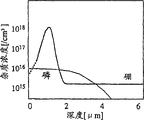
Figure 77 is the profile of semiconductor device that expression has formed the CMOS structure of anti-convention trap.Below with reference to figure, the 101st, P type semiconductor substrate, the 103rd, anti-convention P trap, the 104th, anti-convention N trap, the 124th, element isolating oxide film, the 125th, source/leakage, the 126th, gate oxidation films, the 127th, gate electrode.Figure 78 is the impurities concentration distribution figure of depth direction in the substrate sections of X-X ' section of the semiconductor device of expression shown in Figure 77, and Figure 79 is the inside potential barrier figure in the expression X-X ' section.
By these figure as can be known, because anti-convention P trap is to inject implanted dopant with high energy ion, so can form the peak value of impurity concentration in the degree of depth of in substrate, expecting.Therefore, forming on the anti-convention P trap under the situation of CMOS transistor arrangement, the high concentration part in anti-convention P trap bottom has suppressed impedance, and voltage drop diminishes.Therefore, the electric current amplification factor of parasitic bipolar transistor diminishes, and the generation of locking is become be not easy.
Also have, not only in the CMOS structure, and under the situation that forms anti-convention P trap, the potential barrier that the peak value of the impurity concentration of utilization bottom the anti-convention trap and the mil energy level difference of substrate impurity range produce, hinder the source/leakage 125 that arrives substrate surface for the electronics of minority carrier, improve soft fault preventing.
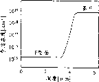
Have, for example Japan's special permission discloses disclosed in the flat 4-212453 again, for improving soft fault preventing, with semiconductor-based chip architecture and the manufacture method thereof of anti-convention N trap impurity layer around anti-convention P trap.
Figure 80 is the profile of expression around the formed semiconductor device substrate sections of N type impurity layer of anti-convention P trap.Among the figure, the 105th, N type impurity layer.On anti-convention P trap, can form NMOS, as the memory block.Figure 81 is the distribution map of the impurity concentration of the depth direction of Y-Y ' section among expression Figure 80.
According to this configuration, owing to the minority carrier that α line etc. produces in substrate, be that electronics is absorbed by this N type impurity layer, hindered it to arrive the source/drop ply (not shown) that forms on the surface of anti-convention P well region, so improved soft fault preventing.
For example, " injecting and autoregistration TiSi at F.S.Lai etc. with the 1MeV ion
21 μ mCMOS technology of the no high locking of processing " disclose among the IEDM Tech.Dig.pp513-516 1985, be to improve soft fault preventing, the structure of the trap of formation low concentration on the substrate of unusual high impurity concentration.
Figure 82 is the profile that is illustrated in the semiconductor device substrate sections that impurity layer is set on the substrate surface with very high p type impurity concentration.Among the figure, the 106th, high concentration P type substrate, the 113rd, P trap, the 104th, anti-convention N trap.On anti-convention N trap 104, form PMOS, on P trap 113, form NMOS, constitute cmos circuit.Figure 83 is the distribution map of the impurity concentration of the depth direction of Z-Z ' section among expression Figure 82.
In this structure, owing to adopt the P type substrate 106 of high concentration, the electric current that has reduced in substrate impedance, the substrate diminishes voltage drop, so can suppress the locking of cmos circuit.
But along with the miniaturization of integrated circuit, in the structure of existing anti-convention trap, soft fault preventing and anti-closed are all very low.
Have again, under the situation of the impurity structure that surrounds anti-convention P trap with N type impurity layer, owing to determine that the terminal as the current potential in intermediate layer is necessary, so miniaturization has been increased structural complexity.
In addition, because the progress on integrated circuit (IC) design and the treatment technology, in same chip, load the memory element of high concentration and high concentration computing circuit integrated circuit create possibility, but in such integrated circuit, the while also needs high soft fault preventing and Gao Nai closed.
Therefore, if adopt the structure that on the high impurity concentration substrate, forms low concentration impurity layer, owing to show high anti-closed, to the CMOS structure is effective, but in the raising of soft fault preventing, there is not effect, after two-layer Fermi (Fermi) energy level difference of back forms potential barrier, hinder diffusion, on the contrary but because of making the soft fault preventing deterioration to the component forming region diffusion to the minority carrier substrate.
In view of the premises, even the object of the present invention is to provide miniaturization also not change soft fault preventing, keep soft fault preventing and anti-closed, semiconductor device and manufacture method thereof simultaneously with the substrate structure that prevents circuit erroneous action.
Semiconductor device of the present invention comprises: the semiconductor chip of the 1st conductivity type, and it has the 1st impurity concentration; Have the 1st impurity layer of the 1st conductivity type, it is formed on the first type surface of described semiconductor chip, and has the 2nd impurity concentration of band impurity concentration peak value; With the 2nd impurity layer of the following side contacts of the 1st impurity layer, it has the 3rd impurity concentration less than the peak concentration of the 1st impurity concentration and described the 2nd impurity concentration; With the element that is formed on described the 1st impurity layer.
Have, semiconductor device has the impurity concentration peak value of the 2nd impurity concentration and the 3rd impurity concentration feature less than the 1st impurity concentration again.
Also have, semiconductor device of the present invention comprises: the semiconductor chip that the 1st conductivity type of the 1st impurity concentration is arranged; Be formed on the first type surface of semiconductor chip and the 1st impurity layer less than the 1st conductivity type of the 2nd impurity concentration of the impurity concentration peak value of the 1st impurity concentration is arranged; The 2nd impurity layer of having with the following side contacts of the 1st impurity layer less than the 2nd conductivity type of the 3rd impurity concentration of the impurity concentration peak value of the 1st impurity concentration; With the element that is formed on the 1st impurity layer.
In addition, semiconductor device of the present invention comprises: the semiconductor chip that the 2nd conductivity type of the 1st impurity concentration is arranged; Be formed on the first type surface of semiconductor chip and the 1st impurity layer of the 1st conductivity type of the 2nd impurity concentration of impurity concentration peak value is arranged; With the following side contacts of the 1st impurity layer, the 2nd impurity layer less than the 3rd impurity concentration of the 1st and the 2nd impurity concentration arranged; With the element that is formed on the 1st impurity layer.
Wherein, to have the 1st impurity layer be anti-convention P trap to semiconductor device, the element that forms on the 1st impurity layer is the feature of MOS transistor npn npn.
Therefore, the feature of semiconductor device of the present invention comprises: the 1st impurity layer is an anti-convention P trap; The element that forms on the 1st impurity layer is a MOS transistor; And the 3rd impurity layer of the 2nd conductivity type that the 4th impurity concentration is arranged that is adjacently formed is mutually arranged on other first type surface of semiconductor chip and the 4th impurity layer of the 1st conductivity type of the 5th impurity concentration is arranged; CMOS transistor that on the surface of the 3rd and the 4th impurity layer, form at least, control MOS transistor npn npn.
And the feature of semiconductor device of the present invention comprises: the 1st impurity layer is an anti-convention P trap; The element that forms on the 1st impurity layer is a MOS transistor; And the 3rd impurity layer of the 2nd conductivity type that the 4th impurity concentration is arranged that is adjacently formed is mutually arranged on other first type surface of semiconductor chip and the 4th impurity layer of the 1st conductivity type of the 5th impurity concentration is arranged; At least form with the following side contacts of the 3rd and the 4th impurity layer, the 5th impurity layer greater than the 1st conductivity type of the 6th impurity concentration of the 1st to the 5th impurity concentration arranged; CMOS transistor that form at the 3rd and the 4th impurity layer at least, control MOS transistor npn npn.
And the feature of semiconductor device of the present invention comprises: the 1st impurity layer is an anti-convention P trap; The element that forms on the 1st impurity layer is a MOS transistor; And the 3rd impurity layer of the 2nd conductivity type that the 4th impurity concentration is arranged that is adjacently formed is mutually arranged on other first type surface of semiconductor chip and the 4th impurity layer of the 1st conductivity type of the 5th impurity concentration is arranged; CMOS transistor that form on the surface of the 3rd and the 4th impurity layer at least, control MOS transistor npn npn.
The manufacture method of semiconductor device of the present invention comprises the following steps: to be formed with the 1st impurity layer less than the 2nd impurity concentration of the 1st impurity concentration on the semiconductor chip first type surface of the 1st conductivity type with the 1st impurity concentration; On the surface of the 1st impurity layer, be formed with the 2nd impurity layer greater than the 3rd impurity concentration that the impurity concentration peak value is arranged of the 2nd impurity concentration; With on the 2nd impurity layer surface, form element.
In addition, the step of manufacturing of semiconductor device of the present invention comprises: formation is less than the 1st impurity layer of the 2nd conductivity type of the 2nd impurity concentration that the impurity peak value is arranged of the 1st impurity concentration on the semiconductor chip first type surface of the 1st conductivity type with the 1st impurity concentration; On the surface of the 1st impurity layer, be formed with the 2nd impurity layer less than the 3rd impurity concentration that the impurity concentration peak value is arranged of the 1st impurity concentration; With on the 2nd impurity layer surface, form element.
And the step of manufacturing of semiconductor device of the present invention also comprises: form the 11st impurity layer that the 2nd impurity concentration is arranged less than the 1st impurity concentration on the first type surface of the semiconductor chip of the 2nd conductivity type with the 1st impurity concentration; On the surface of the 1st impurity layer, be formed with the 2nd impurity layer less than the 1st conductivity type of the 3rd impurity concentration that the impurity concentration peak value is arranged of the 1st impurity concentration; With on the 2nd impurity layer surface, form element.
Also have, this manufacture method is characterised in that, has technology that the epitaxial growth of utilizing forms the 1st impurity layer, utilizes ion to inject the feature of the technology that forms the 2nd impurity layer.
And, the manufacture method of semiconductor device of the present invention comprises the following steps: that also the 3rd impurity layer of the 2nd conductivity type that the 4th impurity concentration is arranged that is adjacently formed is mutually arranged and the 1st conductivity type of the 5th impurity concentration is arranged on other first type surface of semiconductor chip the 4th impurity layer; At least on the surface of the 3rd and the 4th impurity layer, form the CMOS transistor of control MOS transistor.
Have, production process of semiconductor device step of the present invention also comprises again: with the contiguous semiconductor chip of the 1st impurity layer on formation technology greater than the 5th impurity layer of the 1st conductivity type of the 6th impurity concentration of the 1st to the 5th impurity concentration is arranged.
In addition, the manufacture method of semiconductor device of the present invention also comprises: the technology that is formed with on the first type surface of semiconductor chip of the 1st conductivity type of the 1st impurity concentration less than the 1st impurity layer of the 2nd impurity concentration of the 1st impurity concentration is arranged; Form the 2nd impurity layer in the part 1 of the 1st impurity layer less than the 2nd conductivity type that the 3rd impurity concentration is arranged of the 1st impurity concentration; On the surface of the part 1 of the 1st impurity layer, be formed with the 3rd impurity layer greater than the 1st conductivity type of the 4th impurity concentration of the impurity peak value of the 2nd and the 3rd impurity concentration; Formation adjoins each other with the surface of the part 2 of the 1st impurity layer, and the 4th impurity layer and the 5th impurity layer that the 1st conductivity type of the 6th impurity concentration is arranged of the 2nd conductivity type of the 5th impurity concentration arranged; On the surface of the 3rd impurity layer, form the MOS transistor npn npn; At least on the surface of the 4th and the 5th impurity layer, form the CMOS transistor of control MOS transistor.
And the feature of the manufacture method of semiconductor device of the present invention is that also the 1st impurity layer concentration has the impurity concentration peak value greater than the 2nd to the 4th impurity concentration, the 2nd impurity concentration.
Have, the feature of the manufacture method of semiconductor device of the present invention also is again, is formed with the 6th impurity layer greater than the 1st conductivity type of the 7th impurity concentration of the 2nd to the 3rd impurity concentration in the bottom of the part 2 of the 1st impurity layer.
And the feature of the manufacture method of semiconductor device of the present invention also is, utilizes epitaxial growth to form the 1st impurity layer, utilizes ion to inject formation the 3rd to the 5th impurity layer.
Fig. 1 is the semiconductor device profile of the expression embodiment of the invention 1.
Fig. 2 is the semiconductor device substrate profile of the expression embodiment of the invention 1.
Fig. 3 is the distribution map that is shown in impurity concentration in the A-A ' section of semiconductor device substrate of Fig. 2.
Fig. 4 is the inside potential barrier figure that is shown in substrate in the A-A ' section of semiconductor device substrate of Fig. 2.
Fig. 5 is the profile of the method, semi-conductor device manufacturing method of the expression embodiment of the invention 1.
Fig. 6 is the profile of the method, semi-conductor device manufacturing method of the expression embodiment of the invention 1.
Fig. 7 is the profile of the method, semi-conductor device manufacturing method of the expression embodiment of the invention 1.
Fig. 8 is the distribution map that is shown in impurity concentration in the A-A ' section of semiconductor device substrate of Fig. 5.
Fig. 9 is the profile of the semiconductor device substrate of the expression embodiment of the invention 2.
Figure 10 is the distribution map that is shown in impurity concentration in the A-A ' section of semiconductor device substrate of Fig. 9.
Figure 11 is the inside potential barrier figure that is shown in substrate in the A-A ' section of semiconductor device substrate of Fig. 9.
Figure 12 is the profile of the method, semi-conductor device manufacturing method of the expression embodiment of the invention 2.
Figure 13 is the profile of the method, semi-conductor device manufacturing method of the expression embodiment of the invention 2.
Figure 14 is the profile of the method, semi-conductor device manufacturing method of the expression embodiment of the invention 2.
Figure 15 is the profile of the method, semi-conductor device manufacturing method of the expression embodiment of the invention 2.
Figure 16 is the impurities concentration distribution figure that is shown in boron and phosphorus in the A-A ' section of semiconductor device substrate of Figure 14.
Figure 17 is the impurities concentration distribution figure that is shown in boron and phosphorus in the A-A ' section of semiconductor device substrate of Figure 15.
Figure 18 is the profile of the method, semi-conductor device manufacturing method of the expression embodiment of the invention 2.
Figure 19 is the profile of the method, semi-conductor device manufacturing method of the expression embodiment of the invention 2.
Figure 20 is the profile of the method, semi-conductor device manufacturing method of the expression embodiment of the invention 2.
Figure 21 is the impurities concentration distribution figure that is shown in boron and phosphorus in the A-A ' section of semiconductor device substrate of Figure 19.
Figure 22 is the impurities concentration distribution figure that is shown in boron and phosphorus on the depth direction of semiconductor device substrate of Figure 20.
Figure 23 is the profile of the method, semi-conductor device manufacturing method of the expression embodiment of the invention 2.
Figure 24 is the profile of the method, semi-conductor device manufacturing method of the expression embodiment of the invention 2.
Figure 25 is the impurities concentration distribution figure that is shown in boron and phosphorus in the A-A ' section of semiconductor device substrate of Figure 23.
Figure 26 is the impurities concentration distribution figure that is shown in boron and phosphorus in the depth direction of semiconductor device substrate of Figure 24.
Figure 27 is the profile of the semiconductor device substrate of the expression embodiment of the invention 3.
Figure 28 is the distribution map that is shown in impurity concentration in the A-A ' section of semiconductor device substrate of Figure 27.
Figure 29 is the profile of the method, semi-conductor device manufacturing method of the expression embodiment of the invention 3.
Figure 30 is the profile of the method, semi-conductor device manufacturing method of the expression embodiment of the invention 3.
Figure 31 is the distribution map that is shown in impurity concentration in the A-A ' section of semiconductor device substrate of Figure 29.
Figure 32 is the profile of the semiconductor device substrate of the expression embodiment of the invention 4.
Figure 33 is the distribution map that is shown in impurity concentration in the A-A ' section of semiconductor device substrate of Figure 32.
Figure 34 is the profile of the method, semi-conductor device manufacturing method of the expression embodiment of the invention 4.
Figure 35 is the profile of the method, semi-conductor device manufacturing method of the expression embodiment of the invention 4.
Figure 36 is the distribution map that is shown in impurity concentration in the A-A ' section of semiconductor device substrate of Figure 34.
Figure 37 is the distribution map that is shown in the impurity concentration of boron and phosphorus on the depth direction of semiconductor device substrate of Figure 35.
Figure 38 is the profile of the semiconductor device substrate of the expression embodiment of the invention 5.
Figure 39 is the distribution map that is shown in impurity concentration in the A-A ' section of semiconductor device substrate of Figure 38.
Figure 40 is the profile of the method, semi-conductor device manufacturing method of the expression embodiment of the invention 5.
Figure 41 is the profile of the method, semi-conductor device manufacturing method of the expression embodiment of the invention 5.
Figure 42 is the distribution map that is shown in the impurity concentration of boron and phosphorus on the depth direction of semiconductor device substrate of Figure 40.
Figure 43 is the distribution map that is shown in the impurity concentration of boron and phosphorus on the depth direction of semiconductor device substrate of Figure 41.
Figure 44 is the profile of the semiconductor device substrate of the expression embodiment of the invention 6.
Figure 45 is the distribution map that is shown in impurity concentration in the A-A ' section of semiconductor device substrate of Figure 44.
Figure 46 is the distribution map that is shown in the impurity concentration of boron and phosphorus in the A-A ' section of semiconductor device substrate of Figure 44.
Figure 47 is the distribution map of the impurity concentration of boron and phosphorus in the process of method, semi-conductor device manufacturing method of the expression embodiment of the invention 6.
Figure 48 is the profile of the semiconductor device substrate of the expression embodiment of the invention 7.
Figure 49 is the distribution map that is shown in impurity concentration in the A-A ' section of semiconductor device substrate of Figure 48.
Figure 50 is the distribution map that is shown in boron and the impurity concentration of phosphorus on depth direction in the A-A ' section of semiconductor device substrate of Figure 48.
Figure 51 is the distribution map that is shown in impurity concentration in the A-A ' section of semiconductor device substrate of Figure 48.
Figure 52 is the distribution map that is shown in the impurity concentration of boron and phosphorus in the A-A ' section of semiconductor device substrate of Figure 48.
Figure 53 is the profile of the semiconductor device of the expression embodiment of the invention 8.
Figure 54 is the profile of the semiconductor device substrate of the expression embodiment of the invention 8.
Figure 55 is the distribution map that is shown in impurity concentration in the B-B ' section of semiconductor device substrate of Figure 54.
Figure 56 is the profile of the semiconductor device substrate of the expression embodiment of the invention 8.
Figure 57 is the profile of the method, semi-conductor device manufacturing method of the expression embodiment of the invention 8.
Figure 58 is the profile of the method, semi-conductor device manufacturing method of the expression embodiment of the invention 8.
Figure 59 is the profile of the method, semi-conductor device manufacturing method of the expression embodiment of the invention 8.
Figure 60 is the profile of the method, semi-conductor device manufacturing method of the expression embodiment of the invention 8.
Figure 61 is the profile of the method, semi-conductor device manufacturing method of the expression embodiment of the invention 8.
Figure 62 is the profile of the method, semi-conductor device manufacturing method of the expression embodiment of the invention 8.
Figure 63 is the profile of the method, semi-conductor device manufacturing method of the expression embodiment of the invention 8.
Figure 64 is the profile of the semiconductor device substrate of the expression embodiment of the invention 9.
Figure 65 is the profile of the semiconductor device substrate of the expression embodiment of the invention 9.
Figure 66 is the distribution map that is shown in impurity concentration in the C-C ' section of semiconductor device substrate of Figure 64.
Figure 67 is the profile of the method, semi-conductor device manufacturing method of the expression embodiment of the invention 9.
Figure 68 is the profile of the semiconductor device substrate of the expression embodiment of the invention 10.
Figure 69 is the profile of the method, semi-conductor device manufacturing method of the expression embodiment of the invention 10.
Figure 70 is the profile of the semiconductor device substrate of the expression embodiment of the invention 11.
Figure 71 is the distribution map that is shown in impurity concentration in the C-C ' section of semiconductor device substrate of Figure 70.
Figure 72 is the profile of the method, semi-conductor device manufacturing method of the expression embodiment of the invention 11.
Figure 73 is the profile of the semiconductor device substrate of the expression embodiment of the invention 12.
Figure 74 is the profile of the method, semi-conductor device manufacturing method of the expression embodiment of the invention 12.
Figure 75 is the profile of the semiconductor device substrate of the expression embodiment of the invention 13.
Figure 76 is the profile of the method, semi-conductor device manufacturing method of the expression embodiment of the invention 13.
Figure 77 is a profile of representing semiconductor device substrate in the past.
Figure 78 is the figure that is shown in boron impurities and phosphorus on the depth direction of semiconductor device substrate sections of Figure 77.
Figure 79 is the potential barrier figure that is shown on the depth direction of semiconductor device of Figure 77.
Figure 80 is a profile of representing semiconductor device substrate in the past.
Figure 81 is the figure that is shown in boron impurities and phosphorus on the semiconductor device depth direction of Figure 80.
Figure 82 is a profile of representing semiconductor device substrate in the past.
Figure 83 is the figure that is shown in boron impurities and phosphorus on the semiconductor device depth direction of Figure 82.
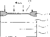
Fig. 1 is the profile of the semiconductor device of the expression embodiment of the invention 1.With reference to figure, the 1st, P type semiconductor substrate, the 2nd, the p type impurity layer that in P type semiconductor substrate 1, forms, the 3rd, the anti-convention P trap that forms in the P type semiconductor substrate 1, the 21st, cell plate, the 23rd, dielectric film, the 24th, cell isolation oxide-film, the 25th, source/leakage, the 26th, gate oxidation films, the 27th, gate electrode, the 28th, silicon oxide film, the 30th, interlayer dielectric, the 31st, bit line.Constitute electric capacity by memory node 22, dielectric film 23 and cell plate 21.
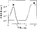
Fig. 2 is the profile of the semiconductor chip of semiconductor device shown in Figure 1, Fig. 3 is the impurities concentration distribution figure in the A-A ' section of semiconductor chip shown in Figure 2, and Fig. 4 is the schematic diagram of the inside potential barrier of substrate in the A-A ' section of semiconductor chip shown in Figure 2.
The substrate of this semiconductor device is 1 * 10 by boron concentration
15~10
16/ cm
3P type semiconductor substrate 1, boron concentration 1 * 10
15/ cm
3P type impurity layer 2, boron concentration 1 * 10
18/ cm
3 Anti-convention trap 3 constitute.
The transistor that forms is gone up on anti-convention P trap 3 surfaces among Fig. 12, can form a plurality of such transistors in practical structures.And, the surperficial 0-0.2 μ m degree of depth of distance place in anti-convention P trap 3, the impurity layer of the blocking-up raceway groove injection that formation has the raceway groove implanted layer of break-through of preventing and threshold value control effect and the inhibition raceway groove forms below isolated oxide film 24 on demand etc.P type impurity layer 2 forms near the bottom of anti-convention P trap 3, and also can not form that a kind of situation in the side of relevant anti-convention trap can.
As shown in Figure 4, structure according to this semiconductor chip, because the existence of p type impurity layer 2, the potential barrier with respect to anti-convention trap top of the electronics that is produced by α line etc. in semiconductor chip 1 just becomes big, hindered electronics to arrive established source/drain region 25 on anti-convention P trap surface, so can suppress the soft error that causes because of electronics.
And, because semiconductor chip 1, p type impurity layer 2 and anti-convention P trap 3 are same conductivity type, and electrically conducting, so needn't distinguish fixed potential individually.Therefore,, number of terminals is not restricted because of being increased on the arrangements of components.Also can obtain the effect of semiconductor integrated circuit miniaturization.
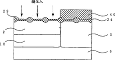
Fig. 5-the 7th, the profile of the manufacture method of the semiconductor device substrate of the expression embodiment of the invention 1.With reference to figure, the 29th, following deposited oxide-film.
Fig. 8 is the distribution map of the impurity concentration in the A-A ' section of expression semiconductor chip shown in Figure 5.
At first, as shown in Figure 5, in boron concentration 1 * 10
16/ cm
3The surface of P type semiconductor substrate 1 on, utilize epitaxial growth, form the boron concentration 1 * 10 of 2-10 μ m
15/ cm
3P type impurity layer 2.Then, as shown in Figure 6, on the surperficial isolated area of p type impurity layer 2, form element isolating oxide film, at the following deposited oxide-film 29 of active area formation as gate oxidation films.But, and do not mind element isolation layer 24 and down deposited oxide layer 29 formation priority in proper order.
Then, as shown in Figure 7,,, after being formed on anti-convention P trap 3 and forming the mask of district's upper openings, press 200keV-1.5meV, 1 * 10 to the resist composition if need
12~1 * 10
14/ cm
2Condition, high-energy injects the ionic state boron of p type impurity, forms anti-convention P trap 3.Then, form transistor, interlayer dielectric, contact hole, electric capacity etc., (not shown) connects up.
As mentioned above, manufacture method according to this semiconductor device, electronics by generations such as α lines in semiconductor chip 1 is big with respect to the potential barrier change on anti-convention trap 3 tops, hinder electronics to arrive the source/drain region 25 that has been formed on the anti-convention P trap 3, can obtain to suppress semiconductor device because of the soft error of electron production.
In addition, because semiconductor chip 1, p type impurity layer 2 and anti-convention P trap 3 are same conductivity type, be electrically conducting, so needn't distinguish fixed potential individually.Therefore,, number of terminals is not restricted because of being increased on the arrangements of components.Also can obtain the effect of semiconductor integrated circuit miniaturization.
And, owing to utilize epitaxial growth to form p type impurity layer 2 concentration of semiconductor chip 1 is raise, so the low semiconductor device of surface impurity concentration of the anti-convention P trap 3 that can obtain at transistor formed.Therefore, becoming in the conducting that makes semiconductor chip 1 and anti-convention P trap 3 is easy to simultaneously, can prevent the deterioration of the transistor characteristic of threshold voltage etc., on manufacturing process, also can widely set the processing range of impurity concentration control etc.
Fig. 9 is the profile of substrate of the semiconductor device of the expression embodiment of the invention 2.Below with reference to figure, the 1st, the P type semiconductor substrate, the 5th, N type impurity layer, the 3rd, anti-convention P trap, and the N type impurity concentration of N type impurity layer 5 is very low, P type semiconductor substrate 1 and anti-convention P trap 3 are on-insulated electric.On this anti-convention P trap 3, can form the element (not shown) the same with embodiment 1.
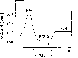
Figure 10 is the impurities concentration distribution figure in the section of A-A ' of expression semiconductor chip shown in Figure 9, and Figure 11 is the figure of the inner potential barrier of substrate in the A-A ' section of expression semiconductor chip shown in Figure 9.
The substrate of this semiconductor device is 1 * 10 by boron concentration
15~10
16/ cm
3P type semiconductor substrate 1, phosphorus concentration 1 * 10
15/ cm
3N type impurity layer 5, boron concentration 1 * 10
18/ cm
3 Anti-convention trap 3 constitute.
In anti-convention P trap 3,, form raceway groove implanted layer on demand, the impurity layer of the blocking-up raceway groove injection that the inhibition raceway groove forms below isolated oxide film 24 etc. with the break-through of preventing and threshold value control effect apart from surperficial 0-0.2 μ m degree of depth place.And N type impurity layer 5 forms near the bottom of anti-convention P trap 3, and also can not form that a kind of situation in the side of relevant anti-convention trap can.
As shown in Figure 11, utilize the existence of N type impurity layer 5, the potential barrier with respect to the top of anti-convention trap of the electronics that is produced by α line etc. in semiconductor chip 1 just becomes big, owing to hindered electronics to arrive established source/drain region on anti-convention P trap 3 surfaces, so can suppress the soft error that causes because of electronics.
In addition, N type impurity layer 5 is different conductivity types with semiconductor chip 1 and anti-convention P trap 3, though semiconductor chip 1 is electrically conductings with anti-convention P trap 3, because N type impurity layer 5 has very low concentration, so needn't fix separately layer current potential individually.Therefore, be not restricted, also can obtain the effect of semiconductor integrated circuit miniaturization because of number of terminals is increased on the arrangements of components.
Figure 12-the 15th, the profile of the manufacture method of the semiconductor device substrate of the expression embodiment of the invention 2, Figure 16 is the distribution map of the impurity concentration of boron and phosphorus in the expression semiconductor chip A-A ' section shown in Figure 14, and Figure 17 is the distribution map of the impurity concentration of boron and phosphorus on the expression semiconductor chip depth direction shown in Figure 15.
At first, as shown in figure 12, in boron concentration 1 * 10
15/ cm
3The first type surface of P type semiconductor substrate 1 on isolated area form element isolating oxide film 24, form following deposited oxide-film 29 at active area as gate oxidation films.But, and do not mind element isolation layer 24 and down deposited oxide layer 29 formation priority in proper order.
Then, as shown in figure 13, if be necessary, on the surface of P type semiconductor substrate,, after being formed on N type impurity layer 5 and forming district's upper openings and constitute masks, press 50keV-200keV, 1 * 10 to the resist composition
11~5 * 10
12/ cm
2Condition, inject the ionic state phosphorus of N type impurity, form N type impurity layer 51.
Then, as shown in figure 14, utilize 1100 ℃ of heat treatments of-1200 ℃, 0.5 hour-3 hours to carry out phosphorous diffusion after, form N type impurity layer 5.
Wherein, under the low situation of the impurity concentration of injecting phosphorus, or under the high situation of heat treatment temperature, or under the long situation of heat treatment time, there is not special problem in p type impurity layer 2 the zone that forms N type impurity layer 5 just forms in embodiment 1 even formed p type impurity layer 2 yet.
Then, as shown in figure 15, if be necessary, on P type semiconductor substrate 1 surface,, after being formed on anti-convention P trap 3 and forming district's upper openings and constitute masks, press 200keV-1.5MeV, 1 * 10 to the resist composition
12~5 * 10
14/ cm
2Condition, high-energy injects the ionic state boron of p type impurity, forms anti-convention trap 3.Then, on this anti-convention P trap 3, form and embodiment 1 components identical (not shown).
As mentioned above, according to the manufacture method of this semiconductor device, make between semiconductor chip 1 and anti-convention P trap 3, can guarantee the N type layer that inserts continue conducting semiconductor device create possibility.Therefore, the potential barrier with respect to anti-convention trap top of the electronics that is produced by α line etc. in semiconductor chip 1 becomes big, hinder electronics to arrive the source/drain region that has been formed on the anti-convention P trap 3, so can obtain to suppress manufacture method because of the semiconductor device of the soft error of electron production.
In addition, N type impurity layer 5 is different conductivity types with semiconductor chip 1 and anti-convention P trap 3, though semiconductor chip 1 is electrically conductings with anti-convention P trap 3, because N type impurity layer 5 has very low concentration, so needn't fix separately layer current potential individually.Therefore, be not restricted, also can obtain the effect of semiconductor integrated circuit miniaturization because of number of terminals is increased on the arrangements of components.
Figure 18-the 20th, the profile of other manufacture method of the semiconductor device substrate of the expression embodiment of the invention 2, Figure 21 is the distribution map of the impurity concentration of boron and phosphorus in the expression semiconductor chip A-A ' section shown in Figure 19, and Figure 22 is the distribution map of the impurity concentration of boron and phosphorus on the expression semiconductor chip depth direction shown in Figure 20.
At first, identical with embodiment 1, in boron concentration 1 * 10
16/ cm
3The surface of P type semiconductor substrate 1 on, utilize epitaxial growth, the boron concentration that forms 2-10 μ m is 1 * 10
15/ cm
3P type impurity layer 2 after, on the surperficial isolated area of p type impurity layer 2, form element isolating oxide film 24, form following deposited oxide-film 29 at active area as gate oxidation films.But, and do not mind element isolating oxide film 24 and down deposited oxide-film 29 formation priority in proper order.
Then, as shown in figure 18,,, form, press 50keV-200keV, 1 * 10 behind the N type impurity layer 5 formation district upper openings formation masks to the resist composition if be necessary
11~1 * 10
13/ cm
2Condition, inject the ionic state phosphorus of N type impurity, form N type impurity layer 51.
Then, as shown in figure 19, utilize 1100 ℃ of heat treatments of-1200 ℃, 0.5 hour-3 hours to carry out phosphorous diffusion after, form N type impurity layer 5.
Wherein, under the low situation of the impurity concentration of injecting phosphorus, under the high situation of heat treatment temperature or under the long situation of heat treatment time, there is not special problem in p type impurity layer 2 the zone that forms N type impurity layer 5 just forms in embodiment 1 even formed p type impurity layer 2 yet.
Then, as shown in figure 20, if be necessary, to the resist composition, formation is pressed 200keV-1.5MeV, 1 * 10 after anti-convention P trap is formed the mask of district's upper opening
12~1 * 10
14/ cm
2Condition, high-energy injects the ionic state boron of p type impurity, forms anti-convention P trap 3.On this anti-convention P trap 3, form and embodiment 1 components identical (not shown) then.
As mentioned above, manufacture method according to this semiconductor device, the potential barrier with respect to anti-convention trap 3 tops of the electronics that is produced by α line etc. in semiconductor chip 1 becomes big, hinder electronics to arrive the source/drain region that has been formed on the anti-convention P trap 3, can obtain to suppress manufacture method because of the semiconductor device of the soft error of electron production.
And,, the concentration of semiconductor chip 1 is raise, so can obtain the low semiconductor device of surface impurity concentration of the anti-convention P trap 3 of transistor formed owing to form N type impurity layer 5 after the epitaxial growth.Therefore, becoming in the conducting that makes semiconductor chip 1 and anti-convention P trap 3 is easy to simultaneously, can prevent the deterioration of the transistor characteristic of threshold voltage etc., on manufacturing process, also can widely set the processing range of impurity concentration control etc.
In addition, N type impurity layer 5 is different conductivity types with semiconductor chip 1 and anti-convention P trap 3, though semiconductor chip 1 is electrically conductings with anti-convention P trap 3, because N type impurity layer 5 has very low concentration, so needn't fix separately layer current potential individually.Therefore, be not restricted because of number of terminals is increased on the arrangements of components, also make miniaturization semiconductor integrated circuit create possibility.
Figure 23-the 24th, the profile of other manufacture method of the semiconductor device substrate of the expression embodiment of the invention 2, Figure 25 is the figure as a result that the impurity fixed point of boron and phosphorus is measured in the expression semiconductor device substrate A-A ' section shown in Figure 23, and Figure 26 is the distribution map of the impurity concentration of boron and phosphorus on the expression semiconductor device substrate depth direction shown in Figure 24.
At first, as shown in figure 23, in boron concentration 1 * 10
16/ cm
3P type silicon chip 1 on, the phosphorus concentration of growth 2-5 μ m is 1 * 10
15/ cm
3N type epitaxial loayer 5 after, on the isolated area on p type impurity layer 2 surface, form element isolating oxide film 24, form following deposited oxide-film 29 at active area as gate oxidation films.But, and do not mind element isolating oxide film 24 and down deposited oxide-film 29 formation priority in proper order.
Then, as shown in figure 24, if be necessary, to the resist composition, formation is pressed 200keV-1.5MeV, 1 * 10 after anti-convention P trap 3 is formed the mask of district's upper openings
12~1 * 10
14/ cm
2Condition, high-energy injects the ionic state boron of p type impurity, forms anti-convention P trap 3.Form and embodiment 1 components identical (not shown) then.
As mentioned above, manufacture method according to this semiconductor device, the potential barrier with respect to anti-convention trap 3 tops of the electronics that is produced by α line etc. in semiconductor chip 1 becomes big, hinder electronics to arrive the source/drain region that has been formed on the anti-convention P trap 3, can obtain to suppress semiconductor device because of the soft error of electron production.
And,, the concentration of semiconductor chip 1 is raise, so can obtain the low semiconductor device of surface impurity concentration of the anti-convention P trap 3 of transistor formed owing to utilize epitaxial growth to form N type impurity layer 5.Therefore, becoming in the conducting that makes semiconductor chip 1 and anti-convention P trap 3 is easy to simultaneously, can prevent the deterioration of the transistor characteristic of threshold voltage etc., on manufacturing process, also can realize the simplification of technology, also can widely set the processing range of impurity concentration control etc.
In addition, N type impurity layer 5 is different conductivity types with semiconductor chip 1 and anti-convention P trap 3, though semiconductor chip 1 is electrically conductings with anti-convention P trap 3, because N type impurity layer 5 has very low concentration, so needn't fix separately layer current potential individually.Therefore, be not restricted because of number of terminals is increased on the arrangements of components, also make miniaturization semiconductor integrated circuit create possibility.
Figure 27 is the profile of substrate of the semiconductor device of the expression embodiment of the invention 3.Below with reference to figure, the 6th, P type semiconductor substrate, the 2nd, the p type impurity layer that forms in the P type semiconductor substrate, the 3rd, the anti-convention P trap that forms in the P type semiconductor substrate 6.
Figure 28 is the distribution map of impurity concentration in the expression semiconductor chip A-A ' section shown in Figure 27.
As shown in figure 28, the substrate of this semiconductor device is 1 * 10 by boron concentration
19/ cm
3High concentration P type semiconductor substrate 6, boron concentration be 1 * 10
15/ cm
3P type impurity layer 2, boron concentration be 1 * 10
18/ cm
3 Anti-convention P trap 3 constitute.
In addition, on anti-convention P trap 3, form a plurality of or single transistor (not shown).Then, in anti-convention P trap 3,, also have to form the situation of impurity layer that has the raceway groove implanted layer of break-through of preventing and threshold value control effect and isolated oxide film 24 below, suppress the blocking-up raceway groove injection etc. of raceway groove formation apart from surperficial 0-0.2 μ m degree of depth place.P type impurity layer 2 forms in the bottom near anti-convention P trap 3, also can not form in the side of relevant anti-convention trap, and that a kind of situation can.
(not shown) under the situation that forms memory element on this substrate structure, by impurities concentration distribution shown in Figure 28 as can be known, the electronics that in P type semiconductor substrate 6, produces by α line etc. with respect to the potential barrier in the anti-convention trap top, because of the existence of p type impurity layer 2 does not become big, in P type semiconductor substrate 6, because the life time of electronics shortens,, has the effect that more can suppress soft error so prevented that electronics from arriving anti-convention P trap 3 surfaces and going up the source/drain region that forms.
In addition, under forming on this substrate structure, utilize the P type semiconductor substrate to make substrate impedance step-down, simultaneously,, have the effect that improves anti-locking owing to formed anti-convention P trap 3 as the transistorized situation of the CMOS of control circuit.
And,, conduct, so needn't distinguish fixed potential individually because P type semiconductor substrate 6, p type impurity layer 2 and anti-convention P trap 3 are same conductivity type.Therefore, even under that a kind of situation that forms memory element CMOS, all do not have to be restricted, also has the effect of semiconductor integrated circuit miniaturization because of number of terminals is increased on the arrangements of components.
Have again, because the concentration of P type semiconductor substrate 6 is higher, the surface impurity concentration that forms transistorized anti-convention P trap 3 is lower, so, becoming in the conducting that makes P type semiconductor substrate 6 and anti-convention P trap 3 is easy to simultaneously, also has the effect of the transistor characteristic deterioration of so-called inhibition threshold voltage etc.
Figure 29-the 30th, the profile of the manufacture method of the semiconductor device substrate of the expression embodiment of the invention 3, Figure 31 are the distribution maps of impurity concentration in the expression semiconductor device substrate A-A ' section shown in Figure 29.
At first, as shown in figure 29, be 1 * 10 in boron concentration
19/ cm
3The surface of high concentration P type semiconductor substrate 6 on, the boron concentration that forms 2-10 μ m is 1 * 10
15/ cm
3P type epitaxial loayer 2.
Then, on the isolated area on P type diamicton 2 surfaces, form element isolating oxide film 24, at the following deposited oxide-film 29 of active area formation as gate oxidation films.But, and do not mind element isolating oxide film 24 and down deposited oxide-film 29 formation priority in proper order.
Then, as shown in figure 20, if be necessary, to the resist composition, formation is pressed 200keV-1.5MeV, 1 * 10 after anti-convention P trap 3 is formed the mask of district's upper openings
12~1 * 10
14/ cm
2Condition, high-energy injects the ionic state boron of p type impurity, forming boron concentration is 1 * 10
18/ cm
2Anti-convention P trap 3.Form single or multiple transistors, interlayer dielectric, contact hole, electric capacity etc. then as required, (not shown) connects up.
In anti-convention P trap 3,, also have to form the situation of impurity layer that has the raceway groove implanted layer of break-through of preventing and threshold value control effect and isolated oxide film 24 below, suppress the blocking-up raceway groove injection etc. of raceway groove formation apart from surperficial 0-0.2 μ m degree of depth place.
P type impurity layer 2 forms in the bottom near anti-convention P trap 3, also can not form in the side of relevant anti-convention trap, and that a kind of situation can
As mentioned above, manufacture method according to this semiconductor device, the electronics that in P type semiconductor substrate 6, produces by α line etc. with respect to the potential barrier in the anti-convention trap top, because of the existence of p type impurity layer 2 does not become big, because the life time of electronics shortens in P type semiconductor substrate 6, so prevented that electronics from arriving anti-convention P trap 3 surfaces and going up the source/drain regions that form, and also can obtain to improve the manufacture method of the semiconductor storage unit of soft fault preventing.
In addition, forming under the transistorized situation of CMOS on this substrate structure, because the concentration of semiconductor chip 6 is higher, so, when making substrate impedance step-down, have the effect of the anti-closed of further raising because of forming anti-convention P trap 3.
And,, conduct, so needn't distinguish fixed potential individually because P type semiconductor substrate 6, p type impurity layer 2 and anti-convention P trap 3 are same conductivity type.Therefore,, be not restricted because of number of terminals is increased on the arrangements of components even under the sort of situation that forms memory element CMOS, make miniaturization semiconductor integrated circuit create possibility.
Have again, owing to utilize epitaxial growth to form p type impurity layer 2, so the concentration of P type semiconductor substrate 6 is higher, the surface impurity concentration that forms transistorized anti-convention P trap 3 becomes lower, becoming in the conducting that makes P type semiconductor substrate 6 and anti-convention P trap 3 is easy to simultaneously, also has the effect of the transistor characteristic deterioration of so-called inhibition threshold voltage etc.
Figure 32 is the profile of substrate of the semiconductor device of the expression embodiment of the invention 4.Below with reference to figure, the 6th, P type semiconductor substrate, the 5th, the N type impurity layer that forms in the P type semiconductor substrate, the 3rd, the anti-convention P trap that forms in the P type semiconductor substrate 6.
Figure 33 is the distribution map of impurity concentration in the expression semiconductor chip A-A ' section shown in Figure 32.
As shown in figure 33, the substrate of this semiconductor device is 1 * 10 by boron concentration
19/ cm
3High concentration P type semiconductor substrate 6, phosphorus concentration be 1 * 10
15/ cm
3N type impurity layer 5, boron concentration be 1 * 10
18/ cm
3 Anti-convention P trap 3 constitute.
In addition, on anti-convention P trap 3, form a plurality of or single transistor (not shown).Then, in anti-convention P trap 3,, also have to form the situation of impurity layer that has the raceway groove implanted layer of break-through of preventing and threshold value control effect and isolated oxide film 24 below, suppress the blocking-up raceway groove injection etc. of raceway groove formation apart from surperficial 0-0.2 μ m degree of depth place.N type impurity layer 5 forms in the bottom near anti-convention P trap 3, also can not form in the side of relevant anti-convention trap, and that a kind of situation can.
Forming on this substrate structure under the situation of memory element, detachable by impurities concentration distribution shown in Figure 33, the electronics that in P type semiconductor substrate 6, produces by α line etc. with respect to the potential barrier in the anti-convention trap top, because of the existence of N type impurity layer 5 does not become big, in P type semiconductor substrate 6, because the life time of electronics shortens,, has the effect that more can suppress soft error so prevented that electronics from arriving anti-convention P trap 3 surfaces and going up the source/drain region that forms.
In addition, under forming on this substrate structure, utilize P type semiconductor substrate 6 to make substrate impedance step-down, simultaneously,, have the effect that improves anti-closed owing to formed anti-convention P trap 3 as the transistorized situation of the CMOS of control circuit.
In addition, though N type impurity layer 5 is different conductivity types with semiconductor chip 6 and anti-convention P trap 3, semiconductor chip 6 is electrically conductings with anti-convention P trap 3, because N type impurity layer 5 has very low concentration, so needn't fix separately layer current potential individually.Therefore, be not restricted, producing effect aspect the miniaturization of semiconductor integrated circuit because of number of terminals is increased on the arrangements of components.
Have again, because the surface impurity concentration of higher, the transistorized anti-convention P of the concentration trap 3 of formation P type semiconductor substrate 6 is lower, be easy to simultaneously so become, also have the effect of the transistor characteristic deterioration of so-called inhibition threshold voltage etc. in the conducting that makes P type semiconductor substrate 6 and anti-convention P trap 3.
Figure 34-the 35th, the profile of the manufacture method of the semiconductor device substrate of the expression embodiment of the invention 4, Figure 36 are the distribution maps of impurity concentration in the expression semiconductor device substrate A-A ' section shown in Figure 34.Figure 37 is the distribution map of the impurity concentration of boron on the expression semiconductor device substrate depth direction shown in Figure 35 and phosphorus.
At first, as shown in figure 34, be 1 * 10 in boron concentration
18-1 * 10
19/ cm
3P type semiconductor substrate 6 on, the epitaxially grown phosphorus concentration that forms 2-10 μ m is 1 * 10
15/ cm
3N type impurity layer 5.
Then, on the isolated area on N type impurity layer 5 surfaces, form element isolating oxide film 24, at the following deposited oxide-film 29 of active area formation as gate oxidation films.But, and do not mind element isolating oxide film 24 and down deposited oxide-film 29 formation priority in proper order.
Then, as shown in figure 35, if be necessary, to the resist composition, formation is pressed 200keV-1.5MeV, 1 * 10 after anti-convention P trap 3 is formed the mask of district's upper openings
12~1 * 10
14/ cm
2Condition, high-energy injects the ionic state boron of p type impurity, forming boron concentration is 1 * 10
18/ cm
2Anti-convention P trap 3.Form single or multiple transistors, interlayer dielectric, contact hole, electric capacity etc. then as required, connect up.
In anti-convention P trap 3,, also have to form the situation of impurity layer that has the raceway groove implanted layer of break-through of preventing and threshold value control effect and isolated oxide film 24 below, suppress the blocking-up raceway groove injection etc. of raceway groove formation apart from surperficial 0-0.2 μ m degree of depth place.
N type impurity layer 5 forms in the bottom near anti-convention P trap 3, also can not form in the side of relevant anti-convention trap, and that a kind of situation can.
As mentioned above, manufacture method according to this semiconductor device, the electronics that in P type semiconductor substrate 6, produces by α line etc. with respect to the potential barrier in the anti-convention trap top, because of the existence of N type impurity layer 5 does not become big, because the life time of electronics shortens in P type semiconductor substrate 6, so prevented that electronics from arriving anti-convention P trap 3 surfaces and going up the source/drain regions that form, and also can obtain to improve the manufacture method of the semiconductor storage unit of soft fault preventing.
In addition, forming on this substrate structure under the transistorized situation of CMOS, because the concentration of semiconductor chip 6 is higher, so, become simultaneously easy in the conducting that makes substrate impedance step-down, semiconductor chip and anti-convention P trap 3, also can obtain further to improve the manufacture method of the semiconductor device of anti-closed.
In addition, N type impurity layer 5 is different conductivity types with semiconductor chip 6 and anti-convention P trap 3, though semiconductor chip 1 is electrically conductings with anti-convention P trap 3, because N type impurity layer 5 has very low concentration, so needn't fix separately layer current potential individually.Therefore, be not restricted because of number of terminals is increased on the arrangements of components, also make miniaturization semiconductor integrated circuit create possibility.
Have again, owing to utilize epitaxial growth to form N type impurity layer 5, so higher in the concentration that can obtain P type semiconductor substrate 6, as to form transistorized anti-convention P trap 3 lower semiconductor device of surface impurity concentration, becoming in the conducting that makes P type semiconductor substrate 6 and anti-convention P trap 3 is easy to simultaneously, also has the effect of the transistor characteristic deterioration of so-called inhibition threshold voltage etc.
Figure 38 is the profile of substrate of the semiconductor device of the expression embodiment of the invention 4.Below with reference to figure, the 6th, P type semiconductor substrate, the 7th, the N type impurity layer that forms in the P type semiconductor substrate, the 3rd, the anti-convention P trap that forms in the P type semiconductor substrate 6.
Figure 39 is the distribution map of impurity concentration in the expression semiconductor chip A-A ' section shown in Figure 38.
As shown in figure 39, the substrate of this semiconductor device is 1 * 10 by boron concentration
19/ cm
3High concentration P type semiconductor substrate 6, phosphorus concentration be 1 * 10
18/ cm
3N type impurity layer 7, boron concentration be 1 * 10
18/ cm
3 Anti-convention P trap 3 constitute.
In addition, on anti-convention P trap 3, form a plurality of or single transistor (not shown).Then, in anti-convention P trap 3,, also have to form the situation of impurity layer that has the raceway groove implanted layer of break-through of preventing and threshold value control effect and isolated oxide film 24 below, suppress the blocking-up raceway groove injection etc. of raceway groove formation apart from surperficial 0-0.2 μ m degree of depth place.N type impurity layer 7 is to be centered around forming of anti-convention P trap 3 on every side.
Forming on this substrate structure under the situation of memory element, by impurities concentration distribution shown in Figure 39 as can be known, in P type semiconductor substrate 6, the life time of electronics does not shorten, become big with respect to the potential barrier in the anti-convention trap top because of the existence of N type impurity layer 7 by the electronics of generations such as α line, so prevented that electronics from arriving the source/drain region that forms on anti-convention P trap 3 surfaces, had the effect that suppresses soft error.
In addition, under forming on this substrate structure as the transistorized situation of the CMOS of control circuit, utilize P type semiconductor substrate 6 to make substrate impedance step-down, simultaneously, owing to formed around anti-convention P trap 3 N type impurity layer 7 on every side, P type substrate 6 and anti-convention P trap 3 are isolated, so have the effect that improves anti-closed.
Figure 40-the 41st, the profile of manufacture method of the semiconductor device substrate of the expression embodiment of the invention 5, Figure 42 are the distribution maps of the impurity concentration of boron and phosphorus on the expression semiconductor device substrate depth direction shown in Figure 40.Figure 43 is the distribution map of the impurity concentration of boron on the expression semiconductor device substrate depth direction shown in Figure 42 and phosphorus.
At first, the same with embodiment 3, be 1 * 10 in boron concentration
18/ cm
3P type semiconductor substrate 6 on, forming and utilizing the epitaxially grown phosphorus concentration of 2-10 μ m is 1 * 10
15/ cm
3P type impurity layer 2.
Then, on the isolated area on p type impurity layer 2 surface, form element isolating oxide film 24, at the following deposited oxide-film 29 of active area formation as gate oxidation films.But, and do not mind element isolating oxide film 24 and down deposited oxide-film 29 formation priority in proper order.
Then, as shown in figure 40,,, form, press 500keV-10MeV, 1 * 10 behind the anti-convention P trap 3 formation district upper openings formation masks to the resist composition if be necessary
12~1 * 10
14/ cm
2Condition, high-energy injects the ionic state phosphorus of N type impurity, forms N type impurity layer 7.
Then, as shown in figure 41,,, form, behind the mask to anti-convention P trap 3 formation district upper openings, press 200keV-1.5MeV, 1 * 10 the resist composition if be necessary
12~1 * 10
14/ cm
2Condition, high-energy injects the ionic state boron of p type impurity, forms anti-convention P trap 3.
Then as required, form single or multiple transistors, interlayer dielectric, contact hole, electric capacity etc., connect up.
Have, forming N type impurity layer 7 and forming in the anti-convention P trap 3, if form the N type impurity layer 7 that centers on anti-convention P trap 3, it is all right which so no matter forms earlier again.
In anti-convention P trap 3,, also have to form the situation of impurity layer that has the raceway groove implanted layer of break-through of preventing and threshold value control effect and isolated oxide film 24 below, suppress the blocking-up raceway groove injection etc. of raceway groove formation apart from surperficial 0-0.2 μ m degree of depth place.
As mentioned above, manufacture method according to this semiconductor device, the electronics that in P type semiconductor substrate 6, produces by α line etc. with respect to the potential barrier in the anti-convention trap top, because of the existence of N type impurity layer 7 does not become big, because the life time of electronics shortens in P type semiconductor substrate 6, so prevented that electronics from arriving anti-convention P trap 3 surfaces and going up the source/drain regions that form, and also can obtain to improve the manufacture method of the semiconductor storage unit of soft fault preventing.
In addition, forming on the structure of this substrate under the transistorized situation of CMOS, on P type half substrate 6, form N type impurity layer 7 and anti-convention P trap 3 owing to utilize epitaxial growth to form p type impurity layer 2 back, so the concentration of semiconductor chip 6 is higher, can obtain to form the lower semiconductor device of surface impurity concentration of transistorized P trap 3.Therefore, when suppressing the transistor characteristic deterioration of threshold voltage etc., utilize lower substrate impedance and anti-convention P trap 3, can obtain to improve the semiconductor device of anti-closed.
Figure 44 is the profile of substrate of the semiconductor device of the expression embodiment of the invention 6.Below with reference to figure, the 11st, N type semiconductor substrate, the 2nd, the p type impurity layer that forms in the N type semiconductor substrate, the 3rd, the anti-convention P trap that forms in the N type semiconductor substrate 11.Figure 45 is the distribution map of impurity concentration in the expression semiconductor chip A-A ' section shown in Figure 44.Figure 46 is expression semiconductor chip A-A shown in Figure 44, the distribution map of the impurity concentration of boron and phosphorus in the section.
As shown in figure 45, the substrate of this semiconductor device is 1 * 10 by phosphorus concentration
16/ cm
3High concentration N type semiconductor substrate 11, boron concentration be 1 * 10
15/ cm
3P type impurity layer 2, boron concentration be 1 * 10
18/ cm
3 Anti-convention P trap 3 constitute.
In addition, on anti-convention P trap 3, form a plurality of or single transistor (not shown).Then, in anti-convention P trap 3,, also have to form the situation of impurity layer that has the raceway groove implanted layer of break-through of preventing and threshold value control effect and isolated oxide film 24 below, suppress the blocking-up raceway groove injection etc. of raceway groove formation apart from surperficial 0-0.2 μ m degree of depth place.P type impurity layer 2 forms in the bottom near anti-convention P trap 3, also can not form in the side of relevant anti-convention trap, and that a kind of situation can.
According to this substrate structure,, improve withstand voltage effect so have owing to relaxed the electric field of anti-convention P trap 3 and semiconductor chip 11.
Have again, because the concentration of semiconductor chip 11 is higher, the surface impurity concentration that forms transistorized anti-convention P trap 3 is lower, so can prevent the transistor characteristic deterioration of threshold voltage etc.
Below, the manufacture method of substrate of the semiconductor device of the embodiment of the invention 6 is described.
At first, the same with embodiment 1 is 1 * 10 at phosphorus concentration
16/ cm
3N type semiconductor substrate 11 on, utilizing the extension of growth 2-10 μ m to form boron concentration is 1 * 10
15/ cm
3P type impurity layer 2 after, form element oxide-film 24, deposited oxide-film 29 down.Figure 47 is the impurity concentration figure on the depth direction of the boron of expression this moment and phosphorus.
Then, the same with embodiment 1, as required, form single or multiple anti-convention P traps 3, transistor, interlayer dielectric, contact hole, electric capacity etc., connect up.
In anti-convention P trap 3,, also have to form the situation of impurity layer that has the raceway groove implanted layer of break-through of preventing and threshold value control effect and isolated oxide film 24 below, suppress the blocking-up raceway groove injection etc. of raceway groove formation apart from surperficial 0-0.2 μ m degree of depth place.
As mentioned above, according to the manufacture method of this semiconductor device, because relaxed the electric field of anti-convention P trap 3 and semiconductor chip 11, so can obtain to have the manufacture method of the semiconductor device that improves withstand voltage effect.
And, because the surface impurity concentration of the concentration height of semiconductor chip 11, the transistorized anti-convention P trap 3 of formation is low, so can prevent the deterioration of the transistor characteristic of threshold voltage etc., on manufacturing process, also can widely set the scope of the process conditions of impurity concentration control etc.
Figure 48 is the profile of substrate of the semiconductor device of the expression embodiment of the invention 7.Below with reference to figure, the 11st, N type semiconductor substrate, the 5th, the N type impurity layer that forms in the N type semiconductor substrate 11, the 3rd, the anti-convention P trap that forms in the N type semiconductor substrate 11.Figure 49 is the distribution map of impurity concentration in the expression semiconductor device substrate A-A ' section shown in Figure 48.Figure 50 is the distribution map of boron and the impurity concentration of phosphorus on depth direction in the expression semiconductor device substrate A-A ' section shown in Figure 48.
It is 1 * 10 that this semiconductor device has by phosphorus concentration
16/ cm
3N type semiconductor substrate 11, phosphorus concentration be 1 * 10
15/ cm
3N type impurity layer 5, boron concentration be 1 * 10
18/ cm
3The substrate structure that constitutes of anti-convention trap layer 3.
It is 1 * 10 that N type semiconductor substrate 11 preferably adopts phosphorus concentration
18/ cm
3Substrate.At this moment, Figure 51 is the distribution map of the impurity concentration in the expression semiconductor device substrate A-A ' section shown in Figure 48, and Figure 52 is the distribution map of the impurity concentration of boron and phosphorus in the expression semiconductor device substrate A-A ' section shown in Figure 48.
In addition, on anti-convention P trap 3, form a plurality of or single transistor (not shown).Then, in anti-convention P trap 3,, also have to form the situation of impurity layer that has the raceway groove implanted layer of break-through of preventing and threshold value control effect and isolated oxide film 24 below, suppress the blocking-up raceway groove injection etc. of raceway groove formation apart from surperficial 0-0.2 μ m degree of depth place.N type impurity layer 5 forms in the bottom near anti-convention P trap 3, also can not form in the side of relevant anti-convention trap, and that a kind of situation can.
According to this substrate structure, utilize N type impurity layer 5, owing to relaxed the electric field of anti-convention P trap 3 and semiconductor chip 11, improve withstand voltage effect so have.
Have again, because the surface impurity concentration of higher, the transistorized anti-convention P of the concentration trap 3 of semiconductor chip 11 is lower, so can prevent the transistor characteristic deterioration of threshold voltage etc.
In addition, the phosphorus degree of depth at N type semiconductor substrate 11 is 1 * 10
18/ cm
3Situation under owing to substrate impedance step-down, formed anti-convention P trap simultaneously, forming under the transistorized situation of CMOS, have the effect that anti-closed is further improved.
Below, the manufacture method of the semiconductor device substrate of the embodiment of the invention 7 is described.
At first, the same with embodiment 2, be 1 * 10 at phosphorus concentration
16/ cm
3N type semiconductor substrate 11 on, utilizing the epitaxial growth of 2-10 μ m to form phosphorus concentration is 1 * 10
15/ cm
3N type impurity layer 5 after, form element isolating oxide film 24, deposited oxide-film 29 down.
Then, identical with embodiment 2, as required, form single or multiple anti-convention P traps 3, transistor, interlayer dielectric, contact hole, electric capacity etc., connect up.
In anti-convention P trap 3,, also have to form the situation of impurity layer that has the raceway groove implanted layer of break-through of preventing and threshold value control effect and isolated oxide film 24 below, suppress the blocking-up raceway groove injection etc. of raceway groove formation apart from surperficial 0-0.2 μ m degree of depth place.
As mentioned above, according to the manufacture method of this semiconductor device, because relaxed the electric field of anti-convention P trap 3 and semiconductor chip 11, so can obtain to have the manufacture method of the semiconductor device that improves withstand voltage effect.
And, because the surface impurity concentration of the concentration height of semiconductor chip 11, the transistorized anti-convention P trap 3 of formation is low, so can prevent the deterioration of the transistor characteristic of threshold voltage etc., on manufacturing process, also can widely set the scope of the process conditions of impurity concentration control etc.
In addition, be 1 * 10 if utilize phosphorus concentration
18/ cm
3N type semiconductor substrate 11, so owing to substrate impedance step-down, formed anti-convention P trap simultaneously and forming under the transistorized situation of CMOS, can obtain to have the manufacture method of the semiconductor device of the anti-closed of further raising.
Figure 53 is the profile of the semiconductor device of the expression embodiment of the invention 8.Below with reference to figure, the 1st, P type semiconductor substrate, the 5th, the N type impurity layer that forms in the P type semiconductor substrate, 3 and 8 is the anti-convention P traps that form in the P type semiconductor substrate, and 4 and 9 is anti-convention N traps, the 24th, and first isolated oxide film, the 25th, source/leakage, the 26th, gate oxidation films, the 27th, gate electrode.
In addition, Figure 54 is the profile of the semiconductor device substrate of the expression embodiment of the invention 8.
It is the element region (memory cell areas) of purpose and to carry out the element region that logical operation is a purpose (logic circuit area) while the bulk information that obtains memory cell areas that this semiconductor device is divided into the information of storing main capacity substantially.
Memory cell areas mainly is made of NMOSFET, and logic circuit area mainly is made of CMOSFET.
Figure 55 is the distribution map of impurity concentration in the semiconductor chip C-C ' section shown in expression Figure 54.In addition, in the semiconductor chip B-B ' section shown in Figure 54 the distribution of impurity concentration just as shown in Figure 10.By Figure 54 as can be known, memory cell areas has the substrate structure identical with embodiment 2.
On anti-convention P trap 3, form a plurality of or single transistor (not shown).Then, in anti-convention P trap 3,, also have to form the situation of impurity layer that has the raceway groove implanted layer of break-through of preventing and threshold value control effect and isolated oxide film 24 below, suppress the blocking-up raceway groove injection etc. of raceway groove formation apart from surperficial 0-0.2 μ m degree of depth place.N type impurity layer 5 forms in the bottom near anti-convention P trap 3, and also can not form that a kind of situation in the side of relevant anti-convention trap can.
On anti-convention P trap 8, anti-convention N trap 4 and anti-convention N trap 9, form a plurality of or single transistor (not shown), form the CMOS of logic circuit area.In this case, also in the anti-convention trap apart from surperficial 0-0.2 μ m degree of depth place, have to form the situation of impurity layer that has the raceway groove implanted layer of break-through of preventing and threshold value control effect and isolated oxide film 24 below, suppress the blocking-up raceway groove injection etc. of raceway groove formation.
In addition, by on anti-convention N trap 4 and anti-convention P trap 3, forming transistor respectively, also can form CMOS as logical circuit.At this moment, on anti-convention P trap, also formed transistor as memory cell.At this moment, in the N type impurity layer 5 inchoate districts shown in Figure 56, also can form trap, can keep the anti-closed of logic circuit area by it through diffusion anti-convention P.
The trap that is used for logic circuit area CMOS can only be a part and the anti-convention N trap 4 of anti-convention P trap 3, on the contrary, and also can be more than the trap described in the present embodiment.
Substrate structure according to memory cell areas, as shown in Figure 10, the potential barrier with respect to anti-convention trap top of the electronics that in P type semiconductor substrate 1, produces by α line etc., because of the existence of N type impurity layer becomes big, hinder electronics to arrive and be formed on anti-convention P trap 3 lip-deep source/drain regions, have the effect that suppresses soft error.
In addition, semiconductor chip 1, N type impurity layer 5 and anti-convention P trap 3 are electrically conductings, needn't distinguish fixing individually current potential separately.Therefore, be not restricted, in the semiconductor integrated circuit miniaturization, produce effect yet because of number of terminals is increased on the arrangements of components.
Figure 57~Figure 63 is the profile of manufacture method of the semiconductor device substrate of the expression embodiment of the invention 8.
At first, shown in Figure 57, be 1 * 10 in boron concentration
15/ cm
3P type semiconductor substrate 1 first type surface on the formation element isolating oxide film 24 of isolated area, form following deposited oxide-film 29 at active area as gate oxidation films.But, and do not mind element isolating oxide film 24 and down deposited oxide-film 29 formation priority in proper order.
Then, shown in Figure 58,, press 50keV-200keV, 1 * 10 to resist 40 compositions, to after the memory cell areas opening
11~1 * 10
12/ cm
2Condition, inject the ionic state phosphorus of N type impurity, on substrate surface, form N type impurity layer 51.After removing resist, shown in Figure 59, utilize 1100 ℃ of heat treatments of-1200 ℃, 0.5 hour-3 hours to carry out phosphorous diffusion, form N type impurity layer 5.
Wherein, under the low situation of the impurity concentration of injecting phosphorus, under the high situation of heat treatment temperature or under the long situation of heat treatment time, shown in Figure 60, p type impurity layer 2 the zone that forms N type impurity layer 5 just forms in embodiment 1 is even and formed p type impurity layer 2 and also do not had special problem.
Then, shown in Figure 61, after once more to resist 40 compositions and anti-convention P trap formation district opening, press 200keV-1.5MeV, 1 * 10 to memory cell areas
12~1 * 10
14/ cm
2Condition, high-energy injects the ionic state boron of p type impurity, forms anti-convention P trap 3.
Then, shown in Figure 62, after forming the part opening, press 200keV-1.5MeV, 1 * 10 to resist 40 compositions and to the NMOSFET in the logic circuit area
12~1 * 10
14/ cm
2Condition, high-energy injects the ionic state boron of p type impurity, forms anti-convention P trap 8.
Then, shown in Figure 63, after forming the part opening, press 300keV-2.5MeV, 1 * 10 to resist 40 compositions and to the PMOSFET in the logic circuit area
12~1 * 10
14/ cm
2Condition, high-energy injects the ionic state phosphorus of N type impurity, forms anti-convention N trap 4 and 9.After this, form transistor, interlayer dielectric, contact hole, electric capacity etc., (not shown) connects up.
Have again, and do not mind formation simultaneously respectively or form anti-convention P trap 3,8 and anti-convention N trap 4,9 separately.In addition, its formation order also can suitably change.
As mentioned above, manufacture method according to this semiconductor device, the potential barrier with respect to anti-convention trap top that is made by the electronics of generations such as α line in semiconductor chip 1 becomes big, hinder electronics to arrive the source/drain region that has been formed on the anti-convention P trap 3, can obtain to suppress the semiconductor device of the soft error that produces because of electronics.
In addition, by making semiconductor chip 1, anti-convention P trap 3 and p type impurity layer 2 or N type impurity layer 5 electrically conductings, just needn't fix current potential separately individually.Therefore, be not restricted because of number of terminals is increased on the arrangements of components, also make miniaturization semiconductor integrated circuit create possibility.
Figure 64 is the profile of semiconductor device substrate of the expression embodiment of the invention 9, and Figure 65 is the profile of other substrate of the semiconductor device of the expression embodiment of the invention 9.Below with reference to figure, the 1st, the P type semiconductor substrate, the 5th, the N type impurity layer that forms in the P type semiconductor substrate 1,3 and 8 is the anti-convention P traps that form in the P type semiconductor substrate 1,4 and 9 is anti-convention N traps, the 10th, the p type impurity layer.
Figure 66 is the distribution map of impurity concentration in the semiconductor chip C-C ' section shown in expression Figure 64.In addition, in the semiconductor chip B-B ' section shown in Figure 64 the distribution of impurity concentration just as shown in Figure 10.
The same with embodiment 8, this semiconductor device be divided into substantially with the information of storing main capacity be purpose element region (memory cell areas) while and the bulk information that obtains memory cell areas to carry out the element region that logical operation is a purpose (logic circuit area).
Memory cell areas mainly is made of NMOSFET, with embodiment 8 identical structure is arranged.Logic circuit area mainly is made of CMOSFET.
On anti-convention P trap 8, anti-convention N trap 4 and anti-convention N trap 9, form a plurality of or single transistor (not shown), form the CMOS of logic circuit area.In this case, also in the anti-convention trap apart from surperficial 0-0.2 μ m degree of depth place, have to form the situation of impurity layer that has the raceway groove implanted layer of break-through of preventing and threshold value control effect and isolated oxide film 24 below, suppress the blocking-up raceway groove injection etc. of raceway groove formation.
In addition, by on anti-convention N trap 4 and anti-convention P trap 3, forming transistor respectively, also can form CMOS as logical circuit.At this moment, on anti-convention P trap 3, form transistor as memory cell.At this moment, in the 10 inchoate district of the p type impurity floor shown in Figure 65, also can keep the anti-closed of logic circuit area by it through diffuseing to form anti-convention P trap 3.
Substrate structure according to this semiconductor device memory cell areas, as shown in Figure 10, the potential barrier with respect to anti-convention trap top of the electronics that in P type semiconductor substrate 1, produces by α line etc., because of the existence of N type impurity layer 5 becomes big, hinder electronics to arrive and be formed on anti-convention P trap 3 lip-deep source/drain regions, have the effect that suppresses soft error.
In addition, when making semiconductor chip 1, anti-convention P trap 3 and 8, p type impurity layer 10 and N type impurity layer 5 or p type impurity layer 2 electrically conducting, needn't distinguish fixing individually current potential separately.Therefore, be not restricted, in the semiconductor integrated circuit miniaturization, produce effect yet because of number of terminals is increased on the arrangements of components.
And, because of there being P type buried layer 10 in the logic circuit area, the substrate impedance is reduced, can improve effective anti-closed to the logic circuit area that high especially anti-closed must be arranged.At this moment, from improving the viewpoint of anti-closed, the peak concentration of expectation P type buried layer is higher than the peak concentration of P trap.
Figure 67 is the profile of the semiconductor device substrate manufacture method of the expression embodiment of the invention 9.
At first, the same with embodiment 8, be 1 * 10 in boron concentration
15/ cm
3The element isolation zone of first type surface of P type semiconductor substrate 1 on form element isolating oxide film 24, after active area forms down deposited oxide-film 29, form low concentration N type layer 5 in memory cell areas.
Wherein, under the low situation of the impurity concentration of injecting phosphorus, when heat treatment temperature is high, or heat treatment time is when long, shown in Figure 60, the p type impurity layer 2 the zone that forms N type impurity layer 5 just forms in embodiment 1 is even and formed p type impurity layer 2 and also do not had special problem.
Then, shown in Figure 67,, press 500keV-10MeV, 5 * 10 to resist 40 compositions, to after the memory cell areas opening
12~1 * 10
16/ cm
2Condition, high-energy injects the ionic state boron of p type impurity, forms p type impurity layer 10.
Then, the same with embodiment 8, form anti-convention P trap 3, anti-convention P trap 8, anti-convention N trap 4 and 9.
Here, and do not mind form anti-convention P trap 3,4,8 and 9, p type impurity layer 10 respectively reversed in order whether.
Then, form transistor, interlayer dielectric, contact hole, electric capacity etc., (not shown) connects up.
As mentioned above, manufacture method according to this semiconductor device, the potential barrier with respect to anti-convention trap top of the electronics that is produced by α line etc. in semiconductor chip 1 becomes big, hinder electronics to arrive and be formed on anti-convention P trap 3 lip-deep source/drain regions, can obtain to suppress the semiconductor device of the soft error that produces because of electronics.
In addition, utilize semiconductor chip 1, anti-convention P trap 3 and 8, p type impurity layer 10 and N type impurity layer 5 or p type impurity layer 2 for same conductivity type and be electrically conducting, so needn't distinguish fixing individually current potential separately.Therefore, be not restricted, make the possibility that creates of semiconductor integrated circuit miniaturization because of number of terminals is increased on the arrangements of components.
And, because of there being P type buried layer 10 in the logic circuit area, the substrate impedance is reduced, can obtain the logic circuit area that high especially anti-closed must be arranged is improved the manufacture method of the semiconductor device of effective anti-closed.At this moment, from improving the viewpoint of anti-closed, the peak concentration of expectation P type buried layer is higher than the peak concentration of P trap.
Figure 68 is the profile of the semiconductor device substrate of the expression embodiment of the invention 10.Below with reference to figure, the 6th, the P type semiconductor substrate, the 5th, the N type impurity layer that forms in the P type semiconductor substrate 6, the 2nd, the p type impurity layer that forms in the P type semiconductor substrate 6,3 and 8 is the anti-convention P traps that form in the P type semiconductor substrate 6,4 and 9 is anti-convention N traps.
This semiconductor device divide into substantially with the storage main capacity information be the element region (memory cell areas) of purpose and while the bulk information that obtains memory cell areas to carry out the element region that logical operation is a purpose (logic circuit area).Memory cell areas mainly is made of NMOSFET, and logic circuit area mainly is made of CMOSFET.
And impurity structure, the memory cell areas of semiconductor chip are the same with embodiment 3, and logical circuit is the same with embodiment 4.
On anti-convention P trap 3, form a plurality of or single transistor (not shown).In anti-convention P trap,, have to form the situation of impurity layer that has the raceway groove implanted layer of break-through of preventing and threshold value control effect and isolated oxide film 24 below, suppress the blocking-up raceway groove injection etc. of raceway groove formation apart from surperficial 0-0.2 μ m degree of depth place.N type impurity layer 5 is forming near the bottom of anti-convention P trap 3, also can not form in the side of relevant anti-convention trap, and a kind of situation portion is passable.
On anti-convention P trap 8, anti-convention N trap 4 and anti-convention N trap 9, form a plurality of or single transistor (not shown), and form the CMOS of logic circuit area.In this case, also in the anti-convention trap apart from surperficial 0-0.2 μ m degree of depth place, have to form the situation of impurity layer that has the raceway groove implanted layer of break-through of preventing and threshold value control effect and isolated oxide film 24 below, suppress the blocking-up raceway groove injection etc. of raceway groove formation.
In addition, by on anti-convention N trap 4 and anti-convention P trap 3, forming transistor respectively, also can form CMOS as logical circuit.At this moment, on anti-convention P trap 3, also formed transistor as memory cell.At this moment, shown in embodiment 9, also can keep the anti-closed of the CMOSFET of logic circuit area by it in such p type impurity floor 2 inchoate district through diffuseing to form anti-convention P trap 3.
Substrate structure according to this semiconductor device memory cell areas, the potential barrier with respect to anti-convention trap top of the electronics that in P type semiconductor substrate 6, produces by α line etc., because of the existence of N type impurity layer 5 does not become big, because the electron lifetime in the P type semiconductor substrate 6, hinder electronics to arrive and be formed on anti-convention P trap 3 lip-deep source/drain regions, have the effect that suppresses soft error.
In addition, semiconductor chip 6, p type impurity layer 2, N type impurity layer 5, anti-convention P trap 3 and 8 are electrically conductings, needn't distinguish fixing individually current potential separately.Therefore, be not restricted, in the semiconductor integrated circuit miniaturization, produce effect yet because of number of terminals is increased on the arrangements of components.
And,, can improve the anti-closed of logic circuit area because the impurity concentration height of semiconductor chip 6 makes substrate impedance step-down.
Have again, owing to utilize epitaxial growth to form N type impurity layer 5, so can obtain the lower semiconductor device of surface impurity concentration that the concentration of P type semiconductor substrate 6 is higher, form transistorized anti-convention P trap 3, therefore, becoming in the conducting that makes P type semiconductor substrate 6 and anti-convention trap is easy to simultaneously, also can prevent to suppress the deterioration of the transistor characteristic of threshold voltage etc.
Figure 69 is the profile of the semiconductor device substrate manufacture method of the expression embodiment of the invention 10.
At first, shown in Figure 69, be 1 * 10 in boron concentration
18/ cm
3The first type surface of P type silicon chip 6 on form 2-10 μ m boron concentration be 1 * 10
15/ cm
3P type epitaxial loayer.
Then, the element isolating oxide film 24 in the surperficial isolated area of formation p type impurity layer 2 is at the following deposited oxide-film 29 of active area formation as gate oxidation films.But, and do not mind element isolating oxide film 24 and down deposited oxide-film 29 formation priority in proper order.
Then, with embodiment 8 the same N type impurity layer 5, anti-convention P trap 3 and 8, anti-convention N trap 4 and 9, the transistors etc. of forming.
As mentioned above, manufacture method according to this semiconductor device, electronics by generations such as α lines in semiconductor chip 6 makes the potential barrier on anti-convention trap top become big, hinder electronics to arrive the source/drain region that has been formed on the anti-convention P trap 3, can obtain to suppress the manufacture method of the semiconductor device of the soft error that produces because of electronics.
In addition, utilize semiconductor chip 6, anti-convention P trap 3 and 8, p type impurity layer 2 and N type impurity layer 5 for same conductivity type and be electrically conducting, so needn't distinguish fixing individually current potential separately.Therefore, be not restricted because of number of terminals is increased on the arrangements of components, make miniaturization semiconductor integrated circuit create possibility.
In addition, because the impurity concentration height of semiconductor chip 6 makes substrate impedance step-down, so can obtain to improve the manufacture method of the semiconductor device of the anti-closed in the logical circuit.
Have again,, can obtain the lower semiconductor device of surface impurity concentration that the concentration of P type semiconductor substrate 6 is higher, form transistorized anti-convention P trap 3 owing to utilize epitaxial growth to form N type impurity layer 5.Therefore, the conducting of P type semiconductor substrate 6 and anti-convention trap is become be easy to simultaneously, also can prevent to suppress the deterioration of the transistor characteristic of threshold voltage etc., on manufacturing process, also can widely set the scope of the process conditions of impurity concentration control etc.
Embodiment 11
Figure 70 is the profile of the semiconductor device substrate of the expression embodiment of the invention 11.Below with reference to figure, the 6th, the P type semiconductor substrate, the 5th, the N type impurity layer that forms in the P type semiconductor substrate 6, the 10th, the p type impurity layer that forms in the P type semiconductor substrate 6,3 and 8 is the anti-convention P traps that form in the P type semiconductor substrate 6,4 and 9 is anti-convention N traps.
This semiconductor device divide into substantially with the information of storing main capacity be the element region (memory cell areas) of purpose and while the bulk information that obtains memory cell areas to carry out the element region that logical operation is a purpose (logic circuit area).Memory cell areas mainly is made of NMOSFET, and logic circuit area mainly is made of CMOSFET.
Figure 71 is the distribution map of impurity concentration in the semiconductor chip C-C ' section shown in expression Figure 70.In addition, the distribution of impurity concentration and embodiment 4 are the same as shown in figure 33 in the semiconductor chip B-B ' section shown in Figure 70.
On anti-convention P trap 3, form a plurality of or single transistor (not shown).Then, in anti-convention P trap 3,, have to form the situation of impurity layer that has the raceway groove implanted layer of break-through of preventing and threshold value control effect and isolated oxide film 24 below, suppress the blocking-up raceway groove injection etc. of raceway groove formation apart from surperficial 0-0.2 μ m degree of depth place.N type impurity layer 5 forms in the bottom near anti-convention P trap 3, also can not form in the side of relevant anti-convention trap, and that a kind of situation can.
On anti-convention P trap 8, anti-convention N trap 4 and anti-convention N trap 9, form a plurality of or single transistor (not shown), and form the CMOS of logic circuit area.In this case, also in the anti-convention trap apart from surperficial 0-0.2 μ m degree of depth place, have to form the situation of impurity layer that has the raceway groove implanted layer of break-through of preventing and threshold value control effect and isolated oxide film 24 below, suppress the blocking-up raceway groove injection etc. of raceway groove formation.
In addition, by on anti-convention N trap 4 and anti-convention P trap 3, forming transistor respectively, also can form CMOS as logical circuit.At this moment, on anti-convention P trap 3, also formed transistor as memory cell.At this moment, shown in embodiment 9, also can keep the anti-closed of the CMOSFET of logic circuit area by it in such p type impurity floor 10 inchoate district through diffuseing to form anti-convention P trap 3.
Substrate structure according to the memory block of this semiconductor device, the electronics that in semiconductor chip 6, produces by α line etc. become big with respect to the potential barrier on anti-convention trap top because of the existence of N type impurity layer 5, hinder electronics to arrive the source/drain region that on anti-convention P trap 3 surfaces, forms, have the effect that suppresses soft error.
In addition, semiconductor chip 6, anti-convention P trap 3 and 8, p type impurity layer 10 and N type impurity layer 5 or p type impurity layer 2 are electrically conductings, needn't distinguish fixing individually current potential separately.Therefore, be not restricted, in the semiconductor integrated circuit miniaturization, produce effect yet because of number of terminals is increased on the arrangements of components.
And,, the substrate impedance is reduced, so can improve effective anti-closed to the logic circuit area that high especially anti-closed must be arranged because not only the impurity concentration of semiconductor chip 6 is higher, and exists P type buried layer 10 in logic circuit area.At this moment, from improving the viewpoint of anti-closed, the peak concentration of expectation p type impurity layer is higher than the peak concentration of anti-convention P trap 3.
Figure 72 is the profile of the semiconductor device substrate manufacture method of the expression embodiment of the invention 11.
At first, the same with embodiment 10, be 1 * 10 in boron concentration
18/ cm
3The first type surface of P type silicon chip 6 on the cell isolation district in form the unit and divide oxidation from film 24, after active area forms down deposited oxide-film 29, form low concentration N type layer in memory cell areas.
Wherein, under the low situation of the impurity concentration of injecting phosphorus, when heat treatment temperature is high, or heat treatment time is when long, p type impurity layer 2 forming in embodiment 1 in the zone that forms N type impurity layer 5 is even and formed p type impurity layer 2 and also do not had special problem.
Then, shown in figure anti-convention anti-convention anti-convention, after resist composition, memory cell areas opening, press 500keV-10MeV, 5 * 10
12~1 * 10
16/ cm
2Condition, high-energy injects the ionic state boron of p type impurity, forms p type impurity layer 10.
Then, the same with embodiment 8, form anti-convention P trap 3, anti-convention P trap 8, anti-convention N trap 4 and 9, transistor etc.
Here, and the formation reversed in order of not minding anti-convention P trap 3,4,8 and 9, p type impurity layer 10 whether.
After this, form transistor, interlayer dielectric, contact hole, electric capacity etc., (not shown) connects up.
As mentioned above, manufacture method according to this semiconductor device, the potential barrier with respect to anti-convention trap top of the electronics that is produced by α line etc. in semiconductor chip 6 becomes big, hinder electronics to arrive and be formed on anti-convention P trap 3 lip-deep source/drain regions, can obtain to suppress the semiconductor device of the soft error that produces because of electronics.
In addition, utilize semiconductor chip 1, anti-convention P trap 3 and 8, p type impurity layer 10 and N type impurity layer 5 or p type impurity layer 2 for same conductivity type and be electrically conducting, so needn't distinguish fixing individually current potential separately.Therefore, be not restricted, make the possibility that creates of semiconductor integrated circuit miniaturization because of number of terminals is increased on the arrangements of components.
And, owing in logic circuit area, there is P type buried layer 10, the substrate impedance is reduced, so can obtain can improve the method for the semiconductor device manufacturing of effective anti-closed to the logic circuit area that high especially anti-closed must be arranged.At this moment, from improving the viewpoint of anti-closed, the peak concentration of expectation P type buried layer is higher than the peak concentration of anti-convention P trap.
Embodiment 12
Figure 73 is the profile of the semiconductor device substrate of the expression embodiment of the invention 12.Below with reference to figure, the 6th, the P type semiconductor substrate, the 7th, the N type impurity layer that forms in the P type semiconductor substrate 6, the 2nd, the p type impurity layer that forms in the P type semiconductor substrate 6,3 and 8 is the anti-convention P traps that form in the P type semiconductor substrate 6,4 and 9 is anti-convention N traps.
This semiconductor device divide into substantially with the information of storing main capacity be the element region (memory cell areas) of purpose and while the bulk information that obtains memory cell areas to carry out the element region that logical operation is a purpose (logic circuit area).Memory cell areas mainly is made of NMOSFET, and logic circuit area mainly is made of CMOSFET.
And impurity structure, the memory cell areas of semiconductor chip are the same with embodiment 5, and logic circuit area is identical with embodiment 3.
On anti-convention P trap 3, form a plurality of or single transistor (not shown).Then, in anti-convention P trap,, have to form the situation of impurity layer that has the raceway groove implanted layer of break-through of preventing and threshold value control effect and isolated oxide film 24 below, suppress the blocking-up raceway groove injection etc. of raceway groove formation apart from surperficial 0-0.2 μ m degree of depth place.
N type impurity layer 7 forms in the bottom near anti-convention P trap 3, also can not form in the side of relevant anti-convention trap, and that a kind of situation can.But, utilize N type impurity layer 7 and anti-convention N trap 4, separate anti-convention P trap 3 and p type impurity layer.
On anti-convention P trap 8, anti-convention N trap 4 and anti-convention N trap 9, form a plurality of or single transistor (not shown), and form the CMOS of logic circuit area.In this case, also in the anti-convention trap apart from surperficial 0-0.2 μ m degree of depth place, have to form the situation of impurity layer that has the raceway groove implanted layer of break-through of preventing and threshold value control effect and isolated oxide film 24 below, suppress the blocking-up raceway groove injection etc. of raceway groove formation.
Substrate structure according to this semiconductor device, utilize the P type semiconductor substrate 6 of high concentration, not only make the lifetime of the electronics in the P type semiconductor substrate 6 of memory cell areas, and owing to utilize anti-convention N trap 4, N type impurity layer 7 electrical isolation anti-convention P traps 3, hinder the electronics that produces by the α line in the P type semiconductor substrate 6 to arrive the source/drain region that on anti-convention P trap 3 surfaces, forms, have the effect that suppresses soft error.
In addition, owing to isolated the anti-convention P trap 3 of memory cell areas and anti-convention P trap 8, the anti-convention N trap 4 and 9 of logic circuit area, thus different current potentials can be arranged, and can move with different substrate bias.
In addition, semiconductor chip 6, p type impurity layer 2 and anti-convention P trap 8 are electrically conductings, needn't distinguish fixing individually current potential separately.Therefore, be not restricted, in the semiconductor integrated circuit miniaturization, produce effect yet because of number of terminals is increased on the arrangements of components.
And, because the concentration height of semiconductor chip 6 makes substrate impedance step-down, have the effect of the anti-closed that improves logic circuit area.
Figure 74 is the profile of the semiconductor device substrate manufacture method of the expression embodiment of the invention 12.
At first, shown in Figure 74, be 1 * 10 in boron concentration
18/ cm
3The first type surface of P type silicon chip 6 on form p type impurity layer 2, form element in its surperficial element marker space and separate oxide-film 24, form deposited oxide-film 29 down at active area.
Then, shown in Figure 74, after resist composition, memory cell areas opening, press 500keV-10MeV, 1 * 10
12~5 * 10
14/ cm
2Condition, high-energy injects the ionic state phosphorus of N type impurity, forms N type impurity layer 7.
Then, the same with embodiment 8, form anti-convention P trap 3, anti-convention P trap 8, anti-convention N trap 4 and 9.
Here, and do not mind form anti-convention P trap 3,4,8 and 9, N type impurity layer 7 respectively reversed in order whether.
After this, form transistor, interlayer dielectric, contact hole, electric capacity etc., (not shown) connects up.
According to the manufacture method of this semiconductor device, because the anti-convention P trap 3 by separating the memory block and anti-convention P trap 8, the anti-convention N trap 4 and 9 of logic circuit area, can obtain the semiconductor device that different potentials, available different substrate bias move.
Substrate structure according to this semiconductor device, utilize the P type semiconductor substrate 6 of high concentration, not only make the lifetime of the electronics in the P type semiconductor substrate 6 of memory cell areas, and owing to utilize anti-convention N trap 4, N type impurity layer 7 electrical isolation anti-convention P traps 3, hinder the electronics that produces by the α line in the P type semiconductor substrate 6 to arrive the source/drain region that on anti-convention P trap 3 surfaces, forms, can obtain further to suppress the manufacture method of the semiconductor device of soft error.
And, because the concentration height of semiconductor chip 6 makes substrate impedance step-down, have the effect of the anti-closed that improves logic circuit area.
Have again, owing to utilize epitaxial growth to form p type impurity layer 2, so in logical circuit, the concentration that can obtain P type semiconductor substrate 6 is higher, the lower semiconductor device of surface impurity concentration that forms transistorized anti-convention P trap 3.Therefore, make the conducting of P type semiconductor substrate 6, p type impurity layer 2 and anti-convention P trap 8 become simultaneously easy, also can prevent to suppress the deterioration of the transistor characteristic of threshold voltage etc., on manufacturing process, also can widely set the scope of the process conditions of impurity concentration control etc.
And, in logical circuit owing to needn't fix independent separately current potential, so be not restricted because of number of terminals is increased on the arrangements of components, make miniaturization semiconductor integrated circuit create possibility.
Embodiment 13
Figure 75 is the profile of the semiconductor device substrate of the expression embodiment of the invention 13.Below with reference to figure, the 6th, the P type semiconductor substrate, the 7th, the N type impurity layer that forms in the P type semiconductor substrate 6, the 10th, the p type impurity layer that forms in the P type semiconductor substrate 6,3 and 8 is the anti-convention P traps that form in the P type semiconductor substrate 6,4 and 9 is anti-convention N traps.
It is the element region (memory cell areas) of purpose and to carry out the element region that logical operation is a purpose (logic circuit area) while the bulk information that obtains memory cell areas that this semiconductor device is divided into the information of storing main capacity substantially.Memory cell areas mainly is made of NMOSFET, and logic circuit area mainly is made of CMOSFET.
And impurity structure, the memory cell areas of semiconductor chip are the same with embodiment 5, and logic circuit area is identical with embodiment 11.
On anti-convention P trap 3, form a plurality of or single transistor (not shown).Then, in anti-convention P trap,, have to form the situation of impurity layer that has the raceway groove implanted layer of break-through of preventing and threshold value control effect and isolated oxide film 24 below, suppress the blocking-up raceway groove injection etc. of raceway groove formation apart from surperficial 0-0.2 μ m degree of depth place.
N type impurity layer 7 forms in the bottom near anti-convention P trap 3, also can not form in the side of relevant anti-convention trap, and that a kind of situation can.But, utilize N type impurity layer 7 and anti-convention N trap 4, separate anti-convention P trap 3 and p type impurity layer 2.
On anti-convention P trap 8, anti-convention N trap 4 and anti-convention N trap 9, form a plurality of or single transistor (not shown), and form the CMOS of logic circuit area.In this case, also in the anti-convention trap apart from surperficial 0-0.2 μ m degree of depth place, have to form the situation of impurity layer that has the raceway groove implanted layer of break-through of preventing and threshold value control effect and isolated oxide film 24 below, suppress the blocking-up raceway groove injection etc. of raceway groove formation.
Substrate structure according to this semiconductor device, utilize the P type semiconductor substrate 6 of high concentration, not only make the lifetime of the electronics in the P type semiconductor substrate 6 of memory cell areas, and owing to utilize anti-convention N trap 4, N type impurity layer 7 electrical isolation anti-convention P traps 3, hinder the electronics that produces by the α line in the P type semiconductor substrate 6 to arrive the source/drain region that on anti-convention P trap 3 surfaces, forms, have the effect that suppresses soft error.
In addition, owing to,, can move with different substrate bias so can obtain different current potentials by the anti-convention P trap 3 of separation memory block and anti-convention P trap 8, the anti-convention N trap 4 and 9 of logic circuit area.
In the logical circuit, semiconductor chip 6,, p type impurity layer 10 and anti-convention P trap 8 be electrically conductings, needn't distinguish fixing individually current potential separately.Therefore, be not restricted, in the semiconductor integrated circuit miniaturization, produce effect yet because of number of terminals is increased on the arrangements of components.
And, because the concentration height of semiconductor chip 6 makes substrate impedance step-down, have the effect of the anti-closed that improves logic circuit area.
Figure 76 is the profile of the semiconductor device substrate manufacture method of the expression embodiment of the invention 13.
At first, the same with embodiment 12, be 1 * 10 in boron concentration
18/ cm
3The first type surface of P type semiconductor substrate 6 on form p type impurity layer 2.Then, forming element in its surperficial element marker space separates oxide-film 24, forms deposited oxide-film 29 down at active area.
Then, shown in Figure 76, after resist composition, memory cell areas opening, press 500keV-10MeV, 5 * 10
12~1 * 10
16/ cm
2Condition, high-energy injects the ionic state boron of p type impurity, forms p type impurity layer 10.
Then, the same with embodiment 8, form anti-convention P trap 3, anti-convention P trap 8, anti-convention N trap 4 and 9.
Here, and do not mind form anti-convention P trap 3,4,8 and 9, N type impurity layer 7 respectively reversed in order whether.
After this, form transistor, interlayer dielectric, contact hole, electric capacity etc., (not shown) connects up.
Manufacture method according to this semiconductor device, because the anti-convention P trap 3 by separating memory cell areas and anti-convention P trap 8, the anti-convention N trap 4 and 9 of logic circuit area, can obtain the semiconductor device that different potentials, available different substrate bias move.
Have again, utilize the P type semiconductor substrate 6 of high concentration, not only make the lifetime of the electronics in the P type semiconductor substrate 6 of memory cell areas, also owing to utilize anti-convention N trap 4, N type impurity layer 7 electric separating anti-convention P traps 3, so hinder the electronics that produces by the α line in the P type semiconductor substrate 6 to arrive the source/drain region that on anti-convention P trap 3 surfaces, forms, can obtain further to suppress the manufacture method of the semiconductor device of soft error.
Owing in logic circuit area, exist the P type semiconductor substrate 6 of high concentration and the P type buried layer 10 that mixes, the substrate impedance is reduced, so can obtain to improve the method for the semiconductor device manufacturing of effective anti-closed to the logic circuit area that high especially anti-closed must be arranged.At this moment, from improving the viewpoint of anti-closed, the peak concentration of expectation P type buried layer is higher than the peak concentration of anti-convention P trap.
Have again, owing to utilize epitaxial growth to form p type impurity layer 2, so in logical circuit, the concentration that can obtain P type semiconductor substrate 6 is higher, the lower semiconductor device of surface impurity concentration that forms transistorized anti-convention trap.Therefore, conducting of P type semiconductor substrate 6, p type impurity layer 10 and anti-convention P trap 8 become be easy to simultaneously, also can prevent to suppress the deterioration of the transistor characteristic of threshold voltage etc., on manufacturing process, also can widely set the scope of the process conditions of impurity concentration control etc.
And, owing to needn't fix independent separately current potential, thus be not restricted because of number of terminals is increased on the arrangements of components, make miniaturization semiconductor integrated circuit create possibility.
Owing to aforesaid structure is arranged, so the present invention has following effect.
The present invention is the existence that utilizes 2nd impurity layer lower than semiconductor chip concentration, what make in the semiconductor chip electronics that produced by the α line becomes big with respect to the potential barrier in the component forming region, owing to hindered electronics to arrive element, can suppress soft error because of electron production.
Have again, because that semiconductor chip and the 1st impurity layer are the concentration of same conductivity type, the 2nd impurity layer is low, so when conducting, needn't fix independent separately current potential.Therefore, be not restricted, in the semiconductor integrated circuit miniaturization, produce effect yet because of number of terminals is increased on the arrangements of components.
And, because the concentration height of semiconductor chip, make that the life time of electronics shortens in the semiconductor chip, prevented that electronics from arriving source/drain region, so have the effect that suppresses soft error.
Have, because the existence of the 2nd impurity layer of the 2nd conductivity type, the potential barrier in the component forming region of the electronics that is produced by α line etc. in semiconductor chip becomes big, owing to hindered electronics to arrive element, can further suppress the soft error because of electron production again.
In addition, owing to utilize the slow electric field that has closed the 1st impurity layer and semiconductor chip of the 2nd impurity layer, realized improving the withstand voltage effect of semiconductor device.
Have again and since in semiconductor chip, produce electronics, become big with respect to the potential barrier of transistor formation region, low in the impurity concentration that forms transistorized the 1st impurity layer surface, thereby can prevent the deterioration of transistor characteristics such as threshold voltage.
In addition,, make the potential barrier with respect to anti-convention trap top of the electronics that produces in the semiconductor substrate become big, suppressed electronics and arrived the source/drain region of the MOS transistor that forms in memory cell areas, so obtained the effect that improves soft fault preventing owing to utilize the 2nd impurity layer.
Have, semiconductor chip, the 1st, the 2nd and the 4th impurity layer are electrically conductings again, there is no need fixing independent separately current potential.Therefore, be not restricted, in the semiconductor integrated circuit miniaturization, produce effect yet because of number of terminals is increased on the arrangements of components.
And, because the concentration height of the 5th impurity layer, so, realized suppressing the effect of the CMOS locking that forms in the logic circuit area.
In addition, owing to utilize the 2nd impurity layer of the 2nd conductivity type, not only make the potential barrier with respect to anti-convention trap top of the electronics that produces in the semiconductor chip become big, and owing to isolated memory cell areas, thereby further suppressed source/drain region that electronics arrives formed MOS transistor in the memory cell areas, so realized improving the effect of anti-soft error.
Have, semiconductor chip, the 4th and the 5th impurity layer are electrically conductings again, there is no need fixing independent separately current potential.Therefore, be not restricted, in the semiconductor integrated circuit miniaturization, produce effect yet because of number of terminals is increased on the arrangements of components.
In addition, utilize to form 2nd impurity layer lower,, hindered electronics to arrive element, so can suppress soft error because of electron production owing to make in the semiconductor chip potential barrier with respect to component forming region of the electronics that produces by α etc. become big than semiconductor chip concentration.
Have again, because semiconductor chip and the 1st impurity layer are that same conductive layer, the 2nd impurity layer concentration are low, there is no need fixing separately respectively current potential separately during electrically conducting, so, be not restricted, also make the manufacturing of the semiconductor integrated circuit of miniaturization become possibility because of number of terminals is increased on the arrangements of components.
Also have, utilize the 2nd impurity layer that forms the 2nd conductivity type with impurity concentration peak value, not only make in the semiconductor chip potential barrier with respect to component forming region of the electronics that produces by α line etc. become big, also because the impurity concentration of semiconductor chip is also big than the 2nd and the 3rd impurity concentration, the life time in the semiconductor chip shortens, so hindered electronics to arrive element, can obtain further to suppress the manufacture method of the semiconductor device of soft error.
And,, can obtain to have the manufacture method of the semiconductor device that improves withstand voltage effect owing to utilize the 1st impurity layer to relax the electric field of semiconductor chip and the 2nd impurity layer.
Have again,, can obtain the lower semiconductor device of impurity concentration that semiconductor chip concentration is higher, form element surface owing to utilize epitaxial growth to form the 1st impurity layer.Therefore, becoming in the conducting that makes semiconductor chip and the 2nd impurity layer is easy to also can prevent the deterioration of transistor characteristics such as threshold voltage simultaneously, on manufacturing process, also can widely set the scope of the process conditions of impurity concentration control etc.
And, utilize the 1st impurity layer, the electronics that in semiconductor chip, produces by α line etc., become big with respect to the potential barrier on the 2nd impurity layer top, hindered electronics to arrive the source/leakage of MOS transistor, can obtain to suppress manufacture method because of the semiconductor device of the soft error of electron production.
Have again, utilizing the 1st, the 2nd and the 4th impurity layer and semiconductor chip is electrically conducting, there is no need respectively fixing independent separately current potential, be not restricted because of number of terminals is increased on the arrangements of components, make miniaturization semiconductor integrated circuit create possibility.
Owing to formed the 5th high impurity layer of impurity concentration, realized suppressing the effect of CMOS transistor locking.
And, utilize the 2nd impurity layer, the electronics that in semiconductor chip, produces by α line etc., become big with respect to the potential barrier on the 3rd impurity layer top, hindered electronics to arrive the source/leakage of MOS transistor, can obtain to suppress the manufacture method of the semiconductor device of the soft error that produces because of electronics.
Have again, utilize the electrically conducting of the 1st, the 5th impurity layer and semiconductor chip, there is no need respectively fixing independent separately current potential, be not restricted because of number of terminals is increased on the arrangements of components, make miniaturization semiconductor integrated circuit create possibility.
In addition, because the concentration height of the 2nd impurity layer, so not only make in the semiconductor chip by the electronics of generations such as α line, become bigger with respect to the potential barrier on the 3rd impurity layer top, also because of having isolated MOS transistor, hinder electronics to arrive source/leakages of MOS transistor, can obtain the method, semi-conductor device manufacturing method of the soft error that further inhibition produces because of electronics.
Also have,, realized suppressing the effect of CMOS transistor locking owing to formed the 6th high impurity layer of impurity concentration.
Have again,, can obtain the lower semiconductor device of surface impurity concentration that semiconductor chip concentration is higher, form transistorized the 3rd, the 4th and the 5th impurity layer owing to utilize epitaxial growth to form the 1st impurity layer.Therefore, becoming in the conducting that makes the 1st or the 6th impurity layer and the 5th impurity layer and semiconductor chip is easy to can prevent the deterioration of transistor characteristics such as threshold voltage simultaneously, on manufacturing process, also can widely set the scope of the process conditions of impurity concentration control etc.
Claims (12)
1. semiconductor device comprises:
The semiconductor chip of one first conductivity type, it has one first impurity concentration;
The anti-convention trap of described first conductivity type, it has second impurity concentration that has the impurity concentration peak value, is formed on the first type surface of described semiconductor chip;
One first impurity layer, it have one the 3rd impurity concentration and with the following side contacts of described anti-convention trap, the 3rd impurity on concentration less than an impurity concentration peak value of described first impurity concentration and the impurity concentration peak value of described second impurity concentration; With
An element that is formed on the described anti-convention trap,
Wherein, described element is the MOS transistor npn npn, and
Described semiconductor device also comprises second impurity layer of one second conductivity type, it has one the 4th impurity concentration, and and the 3rd impurity layer with the 5th impurity concentration of described first conductivity type is adjacent, described second and described the 3rd impurity layer is formed on another first type surface of described semiconductor chip and
A CMOS transistor, it be formed on described at least second and described the 3rd impurity layer on, be used to control described MOS transistor npn npn.
2. semiconductor device according to claim 1,
It is characterized in that the 4th impurity layer of described first conductivity type is formed on below the described at least second and the 3rd impurity layer.
3. semiconductor device according to claim 1,
It is characterized in that described first impurity layer is described second conductivity type.
4. semiconductor device according to claim 1,
It is characterized in that, an impurity concentration peak value of the impurity concentration peak value of described second impurity concentration and described the 3rd impurity concentration on concentration less than the impurity concentration peak value of described first impurity concentration.
5. semiconductor device according to claim 4,
It is characterized in that the 5th impurity layer of described first conductivity type is formed on below the described at least second and the 3rd impurity layer.
6. semiconductor device according to claim 4,
It is characterized in that described first impurity layer is described second conductivity type.
7. semiconductor device according to claim 4,
It is characterized in that described MOS transistor npn npn is the transistor that constitutes a memory cell.
8. semiconductor device according to claim 4,
It is characterized in that the isolation insulating film that described first impurity layer is formed on the first type surface of described semiconductor chip forms deeplyer.
9. semiconductor device according to claim 1,
It is characterized in that described MOS transistor npn npn is the transistor that constitutes a memory cell.
10. semiconductor device according to claim 1,
It is characterized in that the isolation insulating film that described first impurity layer is formed on the first type surface of described semiconductor chip forms deeplyer.
11. semiconductor device according to claim 1,
It is characterized in that, described the 5th impurity concentration has an impurity concentration peak value, and the impurity concentration peak value of described second impurity concentration and described the 5th impurity concentration are formed on the roughly the same degree of depth on the surface of the described semiconductor chip of distance, and have near identical concentration.
12. semiconductor device according to claim 11,
It is characterized in that, the impurity concentration peak value of described second impurity concentration and described the 3rd impurity concentration on concentration less than the impurity concentration peak value of described first impurity concentration.
Applications Claiming Priority (3)
| Application Number | Priority Date | Filing Date | Title |
|---|---|---|---|
| JP22393996A JP3958388B2 (en) | 1996-08-26 | 1996-08-26 | Semiconductor device |
| JP223939/1996 | 1996-08-26 | ||
| JP223939/96 | 1996-08-26 |
Related Child Applications (1)
| Application Number | Title | Priority Date | Filing Date |
|---|---|---|---|
| CNB2003101163756A Division CN1306615C (en) | 1996-08-26 | 1997-08-22 | Semiconductor device and method of manufacturing the same |
Publications (2)
| Publication Number | Publication Date |
|---|---|
| CN1185658A CN1185658A (en) | 1998-06-24 |
| CN1153295C true CN1153295C (en) | 2004-06-09 |
Family
ID=16806078
Family Applications (2)
| Application Number | Title | Priority Date | Filing Date |
|---|---|---|---|
| CNB2003101163756A Expired - Fee Related CN1306615C (en) | 1996-08-26 | 1997-08-22 | Semiconductor device and method of manufacturing the same |
| CNB971186790A Expired - Fee Related CN1153295C (en) | 1996-08-26 | 1997-08-22 | Semiconductor device and mfg. method thereof |
Family Applications Before (1)
| Application Number | Title | Priority Date | Filing Date |
|---|---|---|---|
| CNB2003101163756A Expired - Fee Related CN1306615C (en) | 1996-08-26 | 1997-08-22 | Semiconductor device and method of manufacturing the same |
Country Status (6)
| Country | Link |
|---|---|
| US (1) | US6420763B1 (en) |
| JP (1) | JP3958388B2 (en) |
| KR (1) | KR19980018840A (en) |
| CN (2) | CN1306615C (en) |
| DE (1) | DE19734512A1 (en) |
| TW (1) | TW356597B (en) |
Families Citing this family (14)
| Publication number | Priority date | Publication date | Assignee | Title |
|---|---|---|---|---|
| US6423615B1 (en) * | 1999-09-22 | 2002-07-23 | Intel Corporation | Silicon wafers for CMOS and other integrated circuits |
| US6440805B1 (en) * | 2000-02-29 | 2002-08-27 | Mototrola, Inc. | Method of forming a semiconductor device with isolation and well regions |
| US7145191B1 (en) * | 2000-03-31 | 2006-12-05 | National Semiconductor Corporation | P-channel field-effect transistor with reduced junction capacitance |
| JP2003078032A (en) | 2001-09-05 | 2003-03-14 | Mitsubishi Electric Corp | Semiconductor device and manufacturing method therefor |
| JP2003158204A (en) * | 2001-11-22 | 2003-05-30 | Mitsubishi Electric Corp | Semiconductor storage device and its manufacturing method |
| JP4232477B2 (en) * | 2003-02-13 | 2009-03-04 | パナソニック株式会社 | Verification method of semiconductor integrated circuit |
| EP1683193A1 (en) * | 2003-10-22 | 2006-07-26 | Spinnaker Semiconductor, Inc. | Dynamic schottky barrier mosfet device and method of manufacture |
| JP2005142321A (en) | 2003-11-06 | 2005-06-02 | Nec Electronics Corp | Semiconductor integrated circuit device and its manufacturing method |
| CN101019236A (en) * | 2004-07-15 | 2007-08-15 | 斯平内克半导体股份有限公司 | Metal source power transistor and method of manufacture |
| US20060049464A1 (en) * | 2004-09-03 | 2006-03-09 | Rao G R Mohan | Semiconductor devices with graded dopant regions |
| JP2006344735A (en) * | 2005-06-08 | 2006-12-21 | Seiko Epson Corp | Semiconductor device |
| WO2007047429A1 (en) * | 2005-10-12 | 2007-04-26 | Spinnaker Semiconductor, Inc. | A cmos device with zero soft error rate |
| DE102006023876A1 (en) * | 2006-05-19 | 2007-11-22 | Carl Zeiss Smt Ag | Optical imaging device |
| US7872903B2 (en) * | 2009-03-19 | 2011-01-18 | Altera Corporation | Volatile memory elements with soft error upset immunity |
Family Cites Families (19)
| Publication number | Priority date | Publication date | Assignee | Title |
|---|---|---|---|---|
| US4442591A (en) * | 1982-02-01 | 1984-04-17 | Texas Instruments Incorporated | High-voltage CMOS process |
| US4470191A (en) * | 1982-12-09 | 1984-09-11 | International Business Machines Corporation | Process for making complementary transistors by sequential implantations using oxidation barrier masking layer |
| US4633289A (en) | 1983-09-12 | 1986-12-30 | Hughes Aircraft Company | Latch-up immune, multiple retrograde well high density CMOS FET |
| US4710477A (en) | 1983-09-12 | 1987-12-01 | Hughes Aircraft Company | Method for forming latch-up immune, multiple retrograde well high density CMOS FET |
| DE3340560A1 (en) * | 1983-11-09 | 1985-05-15 | Siemens AG, 1000 Berlin und 8000 München | METHOD FOR THE SIMULTANEOUS PRODUCTION OF FAST SHORT-CHANNEL AND VOLTAGE-RESISTANT MOS TRANSISTORS IN VLSI CIRCUITS |
| US4764482A (en) * | 1986-11-21 | 1988-08-16 | General Electric Company | Method of fabricating an integrated circuit containing bipolar and MOS transistors |
| JPS6410656A (en) * | 1987-07-03 | 1989-01-13 | Hitachi Ltd | Complementary type semiconductor device |
| CN1020028C (en) * | 1987-08-18 | 1993-03-03 | 联邦德国Itt工业股份有限公司 | Method of fabricating implanted wells and islands of cmos integrated circuits |
| JPH0196962A (en) * | 1987-10-08 | 1989-04-14 | Nissan Motor Co Ltd | Vertical mos transistor and manufacture thereof |
| JP2660056B2 (en) | 1989-09-12 | 1997-10-08 | 三菱電機株式会社 | Complementary MOS semiconductor device |
| JP2523409B2 (en) | 1990-05-02 | 1996-08-07 | 三菱電機株式会社 | Semiconductor memory device and manufacturing method thereof |
| KR950009893B1 (en) * | 1990-06-28 | 1995-09-01 | 미쓰비시 뎅끼 가부시끼가이샤 | Semiconductor memory device |
| JP2978345B2 (en) | 1992-11-26 | 1999-11-15 | 三菱電機株式会社 | Method for manufacturing semiconductor device |
| JPH0758212A (en) * | 1993-08-19 | 1995-03-03 | Sony Corp | Cmos integrated circuit |
| JP2682425B2 (en) | 1993-12-24 | 1997-11-26 | 日本電気株式会社 | Method for manufacturing semiconductor device |
| US5393679A (en) | 1994-04-05 | 1995-02-28 | United Microelectronics Corporation | Use of double charge implant to improve retrograde process PMOS punch through voltage |
| JPH07312423A (en) * | 1994-05-17 | 1995-11-28 | Hitachi Ltd | Mis type semiconductor device |
| US5654213A (en) * | 1995-10-03 | 1997-08-05 | Integrated Device Technology, Inc. | Method for fabricating a CMOS device |
| US5767556A (en) * | 1996-02-21 | 1998-06-16 | Nec Corporation | Field effect transistor |
-
1996
- 1996-08-26 JP JP22393996A patent/JP3958388B2/en not_active Expired - Fee Related
-
1997
- 1997-07-31 TW TW086110966A patent/TW356597B/en not_active IP Right Cessation
- 1997-08-08 DE DE19734512A patent/DE19734512A1/en not_active Ceased
- 1997-08-21 KR KR1019970039793A patent/KR19980018840A/en not_active Application Discontinuation
- 1997-08-22 CN CNB2003101163756A patent/CN1306615C/en not_active Expired - Fee Related
- 1997-08-22 CN CNB971186790A patent/CN1153295C/en not_active Expired - Fee Related
- 1997-08-26 US US08/917,528 patent/US6420763B1/en not_active Expired - Fee Related
Also Published As
| Publication number | Publication date |
|---|---|
| US20020020888A1 (en) | 2002-02-21 |
| KR19980018840A (en) | 1998-06-05 |
| CN1501504A (en) | 2004-06-02 |
| CN1185658A (en) | 1998-06-24 |
| US6420763B1 (en) | 2002-07-16 |
| TW356597B (en) | 1999-04-21 |
| CN1306615C (en) | 2007-03-21 |
| JPH1070250A (en) | 1998-03-10 |
| DE19734512A1 (en) | 1998-03-05 |
| JP3958388B2 (en) | 2007-08-15 |
Similar Documents
| Publication | Publication Date | Title |
|---|---|---|
| CN1199281C (en) | Semiconductor unit and its making process | |
| CN1230888C (en) | Semiconductor element and producing method thereof | |
| CN1187839C (en) | Kusunoki Shigeru | |
| CN1135626C (en) | Semiconductor devices and manufacturing method | |
| CN1142586C (en) | Semiconductor integrated circuit device and process for manufacturing the same | |
| CN1230915C (en) | MIM capacitor | |
| CN1231978C (en) | Insulated-gate semiconductor apparatus | |
| CN1610118A (en) | Semiconductor device group and producing method thereof, semiconductor device and producing method thereof | |
| CN1153295C (en) | Semiconductor device and mfg. method thereof | |
| CN1162912C (en) | Semiconductor device and method for mfg. same | |
| CN1445838A (en) | Semiconductor device and manufacturing method thereof | |
| CN1221220A (en) | Semiconductor device comprising capacitor and method of fabricating the same | |
| CN1992523A (en) | Switch circuit and diode | |
| CN1841744A (en) | Semiconductor device incorporating protective diode with stable ESD protection capabilities | |
| CN1790912A (en) | Semiconductor integrated circuit device | |
| CN1666325A (en) | Vertical junction field-effect transistor and method of manufacturing the same | |
| CN1976229A (en) | Semiconductor integrated circuit and method of reducing leakage current | |
| CN1790743A (en) | Transistor and method of manufacturing the same | |
| CN1199248A (en) | Semiconductor device and mfg. method thereof | |
| CN1967850A (en) | Semiconductor device | |
| CN1402356A (en) | Semiconductor device of longitudinal structure | |
| CN1153302C (en) | Thin film transistor and making method | |
| CN1613153A (en) | Semiconductor storage device and its manufacturing method | |
| CN1783499A (en) | Semiconductor memory device | |
| CN1256775C (en) | Semiconductor device and manufacturing method thereof |
Legal Events
| Date | Code | Title | Description |
|---|---|---|---|
| C10 | Entry into substantive examination | ||
| SE01 | Entry into force of request for substantive examination | ||
| C06 | Publication | ||
| PB01 | Publication | ||
| C14 | Grant of patent or utility model | ||
| GR01 | Patent grant | ||
| C17 | Cessation of patent right | ||
| CF01 | Termination of patent right due to non-payment of annual fee |
Granted publication date: 20040609 Termination date: 20100822 |