Disclosure of Invention
Aiming at the defects in the prior art, the invention provides a wafer plasma cleaning method, which has the following specific technical scheme:
a wafer plasma cleaning method comprises the following steps:
one surface of the wafer is cleaned by adopting plasma cleaning equipment, and the array type high-temperature plasma jet flow generated by the plasma cleaning equipment is used for spraying and cleaning the surface of the low-temperature wafer.
According to further optimization of the technical scheme, the plasma cleaning equipment comprises a high-temperature plasma jet generator and a driving type containing basket for containing wafers, wherein the high-temperature plasma jet generator comprises an insulating base, a plurality of groups of spraying nozzle assemblies distributed on one side of the insulating base in an array manner, a first air tank, a second air tank and a high-frequency high-voltage generator, the spraying nozzle assemblies are installed on the other side of the insulating base and comprise a conductive outer pipe, a capillary conductive pipe, a ceramic sleeve and a capillary metal pipe, the capillary conductive pipe is coaxially arranged with the conductive outer pipe, the ceramic pipe is communicated between the tail end of the capillary conductive pipe and an inner cavity of the second air tank, and the capillary conductive pipe is embedded in the insulating base; the conductive outer pipe comprises a circular-pipe-shaped first conductive pipe section, a circular-pipe-shaped second conductive pipe section and a conductive contraction pipe section, wherein the circular-pipe-shaped first conductive pipe section is fixedly arranged on the side wall of the insulating base, the inner diameter of the circular-pipe-shaped second conductive pipe section is smaller than that of the first conductive pipe section, the conductive contraction pipe section is used for connecting the first conductive pipe section and the second conductive pipe section, the head end of the capillary conductive pipe is arranged inside the conductive contraction pipe section, one end of the ceramic sleeve is communicated with the inner cavity of the second conductive pipe section, the other end of the ceramic sleeve is communicated with the tail end of the capillary metal pipe, and a space is formed between the second conductive pipe section and the capillary metal pipe; one output electrode of the high-frequency high-voltage generator is electrically connected with the conductive outer tube, and the other output electrode of the high-frequency high-voltage generator is electrically connected with the capillary conductive tube; a plurality of insulating pipes are communicated between the inner cavity of the first conductive pipe section and the inner cavity of the first air box; the high-temperature plasma jet generator further comprises an electromagnetic induction heating assembly used for heating the capillary metal tube, the electromagnetic induction heating assembly comprises a metal disc and an induction coil, a through hole for the capillary metal tube to pass through is formed in the surface of the metal disc, and the metal disc and the capillary metal tube are connected into a whole.
According to the technical scheme, the outer side of the head of the capillary conductive tube is provided with a plurality of opening seams, the opening seams are arranged along the axial direction of the capillary conductive tube, one end of each opening seam extends to the head end of the capillary conductive tube, a space is arranged between the other end of each opening seam and the tail end of the capillary conductive tube, and the other end of each opening seam is arranged inside the first conductive tube section.
According to further optimization of the technical scheme, the plasma cleaning equipment further comprises a cooling gas injection assembly for cooling the wafer, wherein the cooling gas injection assembly comprises an air injection pipe with an L-shaped cross section, a hose connected with a cooling gas source and a first cylinder for lifting the air injection pipe, the air injection pipe comprises a transverse pipe section positioned on one side of the wafer and a vertical pipe section vertical to the transverse pipe section, and the capillary metal pipe is arranged on one side of the wafer; and a connecting plate is fixedly arranged between the piston rod of the first cylinder and the vertical pipe section.
In a further optimization of the above technical solution, the inner diameter of the second conductive pipe section is equal to the inner diameter of the capillary conductive pipe, and the inner diameter of the second conductive pipe section is equal to the inner diameter of the capillary metal pipe.
According to the technical scheme, the driving type containing basket comprises two side rollers which are arranged in an axial symmetry mode, a carrier roller for supporting the wafer and a fixing rod for fixing the side rollers, wherein a plurality of slots which are arranged at equal intervals and matched with the edge of the wafer are formed in the inner sides of the side rollers, the two side rollers and the carrier roller are arranged in an isosceles triangle structure, and a roller shaft of the carrier roller is connected with the tail end of the fixing rod in a rotating mode.
According to the technical scheme, the driving type containing basket further comprises a sliding type driving mechanism used for driving the carrier roller to rotate, the sliding type driving mechanism comprises a gear fixedly mounted at the tail end of the carrier roller, a toothed roller engaged with the gear, an extension shaft coaxially connected with a roller shaft of the carrier roller, a fixing ring sleeved outside the extension shaft, a circular baffle fixedly mounted at the tail end of the extension shaft, a slot head matched with the baffle, a second cylinder, a supporting seat used for supporting the toothed roller and a speed reduction motor used for driving the toothed roller to rotate, the roller shaft of the toothed roller is rotatably connected with the supporting seat, the toothed roller is arranged below the gear, and a piston rod of the second cylinder is fixedly connected with the slot head.
According to the further optimization of the technical scheme, a water tank is arranged below the carrier roller, and deionized water is contained in the water tank.
According to the further optimization of the technical scheme, the working gas of the plasma cleaning equipment adopts the mixed gas of the first gas and the argon gas to generate high-temperature plasma jet, and the high-temperature plasma jet faces the front side of the wafer to be sprayed and cleaned; the first gas is a mixed gas of hydrogen peroxide mist and air, and compressed air at 2-4 ℃ is sprayed on the back of the wafer to cool.
According to the further optimization of the technical scheme, the volume ratio of the first gas to argon is 1 (5.1-5.8), the mixed gas of the hydrogen peroxide mist and air is the first gas, and the volume fraction of the hydrogen peroxide mist in the first gas is 3.1%; the average temperature of the high-temperature plasma jet is 500-550 ℃.
The invention has the beneficial effects that:
the wafer plasma cleaning method can spray and clean the surface of the wafer by adopting the array type high-temperature plasma jet under normal pressure, can effectively remove particles and organic thin pollutants on the surface of the wafer, has high cleaning efficiency and good cleaning effect, and can reduce the occurrence of secondary pollution.
Detailed Description
In order to make the objects, technical solutions and advantages of the present invention more apparent, the present invention is described in further detail below with reference to the accompanying drawings and embodiments. It should be understood that the specific embodiments described herein are merely illustrative of the invention and are not intended to limit the invention.
Example 1
The wafer plasma cleaning method comprises the following steps:
one surface of the wafer is cleaned by adopting plasma cleaning equipment, and the array type high-temperature plasma jet flow generated by the plasma cleaning equipment is used for spraying and cleaning the surface of the low-temperature wafer.
The working gas can adopt a mixed gas of a first gas and argon to generate high-temperature plasma jet containing high-density free radicals, the first gas is a mixed gas of hydrogen peroxide mist and air, and the hydrogen peroxide mist is vaporous hydrogen peroxide or gaseous hydrogen peroxide; the air is conventional air, and the water vapor content (volume fraction) of the air is not more than 0.03%; the back surface of the wafer is sprayed by compressed air at 2-4 ℃ for cooling, the high-temperature plasma jet is sprayed to the front surface of the wafer, particles and organic thin pollutants on the surface of the wafer are removed, and secondary pollution is reduced.
The volume ratio of the first gas to the argon gas is 1 (5.1-5.8), the mixed gas of the hydrogen peroxide mist and the air is the first gas, and the volume fraction of the hydrogen peroxide mist in the first gas is 3.1%. The average temperature of the high-temperature plasma jet is 500-550 ℃, and the rotating speed of the wafer is 1-2 r/min.
The preparation method of the mixed gas of the hydrogen peroxide mist and the air and the mixed gas of the argon comprises the steps of firstly preparing the hydrogen peroxide mist into hydrogen peroxide mist in a clean room by using an atomizing nozzle, and then pressurizing and conveying the air containing the hydrogen peroxide mist in the clean room by using a high-pressure fan for driving.
The method of producing compressed air and then introducing the compressed air into the hydrogen peroxide-containing gas washing bottle is not recommended because of poor mixing effect. It is also not recommended that the air containing the mist of hydrogen peroxide be produced first and then delivered under pressure using an air compressor, since the air compressor filters out the mist of hydrogen peroxide.
Example 2
Specifically, as shown in fig. 1 and 2, the plasma cleaning apparatus includes a high temperature plasma jet generator 20 and a driving type holding basket for holding the wafer 10, where the high temperature plasma jet generator 20 includes an insulating base 21, a plurality of sets of spray nozzle assemblies distributed in an array on one side of the insulating base 21, a first air tank 22 and a second air tank 23 installed on the other side of the insulating base 21, and a high frequency and high voltage generator 24, the spray nozzle assemblies include a conductive outer tube, a capillary conductive tube 26 coaxially arranged with the conductive outer tube, a ceramic sleeve 27, and a capillary metal tube 28, a ceramic tube 232 is communicated between a tail end of the capillary conductive tube 26 and an inner cavity of the second air tank 23, and the capillary conductive tube 26 is embedded in the insulating base 21; the conductive outer tube comprises a circular tube-shaped first conductive tube section 251 fixedly mounted on the side wall of the insulating base 21, a circular tube-shaped second conductive tube section 253 with the inner diameter smaller than that of the first conductive tube section 251, and a conductive contraction tube section 252 for connecting the first conductive tube section 251 with the second conductive tube section 253, wherein the head end of the capillary conductive tube 26 is arranged inside the conductive contraction tube section 252, one end of the ceramic sleeve 27 is communicated with the inner cavity of the second conductive tube section 253, the other end of the ceramic sleeve 27 is communicated with the tail end of the capillary metal tube 28, an inner ring 271 integrally connected with the inner wall of the ceramic sleeve 27 is arranged at the communication part of the ceramic sleeve 27 and the capillary metal tube 28, and a gap is arranged between the second conductive tube section 253 and the capillary metal tube 28; one output electrode of the high-frequency high-voltage generator 24 is electrically connected with the conductive outer tube, and the other output electrode of the high-frequency high-voltage generator 24 is electrically connected with the capillary conductive tube 26; a plurality of insulating pipes 222 are communicated between the inner cavity of the first conducting pipe section 251 and the inner cavity of the first air box 22; the insulating tube 222 penetrates through the insulating base 21, the high-temperature plasma jet generator 20 further comprises an electromagnetic induction heating assembly for heating the capillary metal tube 28, the electromagnetic induction heating assembly comprises a metal disc 292 and an induction coil 291, a through hole for the capillary metal tube 28 to penetrate through is formed in the surface of the metal disc 292, and the metal disc 292 and the capillary metal tube 28 are connected into a whole (such as full-weld welding).
A first air inlet pipe 221 communicated with the inner cavity of the first air box 22 is arranged outside the first air box 22, and a second air inlet pipe 231 communicated with the inner cavity of the second air box 23 is arranged outside the second air box 23.
First, the first gas inlet pipe 221 is externally connected with an argon gas source (such as an argon gas bottle), and argon gas enters the conductive outer tube through the first gas inlet pipe 221 after passing through the inner cavity of the first gas box 22 and the insulating tube 222 in sequence. The first gas passes through the inner cavity of the second gas box 23, the ceramic tube 232 and the capillary conductive tube 26 in sequence through the second gas inlet pipe 231. The high-frequency high-voltage generator 24 is externally connected with a 220V power supply, the conductive outer tube and the capillary conductive tube 26 are equivalent to two electrodes, plasma discharge is generated between the two electrodes, a large amount of free radicals are generated, the free radicals are contracted by the conductive contraction tube section 252, pass through the second conductive tube section 253 and the ceramic sleeve 27 in sequence, are finally sprayed out of the capillary metal tube 28, and can be further heated at the capillary metal tube 28; the high temperature plasma jet is ejected from the capillary metal tube 28, and after reaching the front surface of the wafer, the high temperature plasma jet reacts with organic pollutants on the surface of the wafer to generate reaction byproducts such as carbon dioxide or water, and then the reaction byproducts are washed away under the flowing of the air flow.
The ceramic sleeve 27 is mainly used for installation, plays an insulating role, and prevents the capillary metal tube 28 from directly contacting the conductive outer tube to bring electrical connection. The inner ring 271 is for ease of installation of the capillary metal tube 28. The capillary metal tubes 28 are made of metal materials, are designed conventionally, adopt capillary structures, and are distributed in an array form with other surrounding capillary metal tubes 28, so that the gathering and binding effects are achieved, and the cleaning effect is improved.
If no electromagnetic induction heating assembly is provided or is not operating, the temperature of the plasma jet emitted from the capillary metal tube 28 will generally not exceed 250 ℃.
When the electromagnetic induction heating assembly works, the induction coil 291 is electrified, the metal disc 292 is preferably made of ferromagnetic materials, and the induction coil 291 performs induction heating on the metal disc 292, so that the temperature of plasma jet ejected from the capillary metal tube 28 can reach 500-550 ℃.
The free radicals are sprayed onto the surface of the wafer to be cleaned after being bound and gathered by the capillary metal tube 28, and then react with organic substances on the surface to generate reaction byproducts such as carbon dioxide, water and the like, so that the purpose of cleaning the organic substances (such as photoresist) on the surface is achieved.
In some embodiments, as shown in fig. 5, a plurality of open slits 261 are disposed on the outer side of the head portion of the capillary conductive tube 26, the open slits 261 are disposed along the axial direction of the capillary conductive tube 26, one end of the open slits 261 extends to the head end of the capillary conductive tube 26, a distance is disposed between the other end of the open slits 261 and the tail end of the capillary conductive tube 26, and the other end of the open slits 261 is disposed inside the first conductive tube segment 251.
The open slit 261 is provided so that the first gas in the capillary tube 26 can be ejected from the open slit 261 and rapidly mixed with the argon gas in the conductive outer tube, and in the above process, ionization occurs simultaneously, thereby generating plasma.
In some embodiments, as shown in fig. 1, the plasma cleaning apparatus further includes a cooling gas injection assembly for cooling the wafer 10, the cooling gas injection assembly includes a gas injection pipe 51 having an L-shaped cross section, a hose 52 connected to a cooling gas source, and a first cylinder 55 for elevating and lowering the gas injection pipe 51, the gas injection pipe 51 includes a horizontal pipe section located at one side of the wafer 10, a vertical pipe section perpendicular to the horizontal pipe section, and the capillary metal pipe 28 is disposed at one side of the wafer 10; a connecting plate 53 is fixedly arranged between the piston rod of the first air cylinder 55 and the vertical pipe section.
The hose 52 can be connected with a gas cylinder, compressed air is stored in the gas cylinder, the temperature of the gas cylinder is reduced to-5-0 ℃, the compressed air in the gas cylinder finally aims at the center of the back of the wafer 10 through the hose 52, the vertical pipe section and the horizontal pipe section, and the compressed air at 2-4 ℃ is jetted out of the horizontal pipe section to reduce the temperature of the back of the wafer 10.
Because the front surface of the wafer 10 is impacted by the high-temperature plasma jet of 500-550 ℃, the back surface of the wafer 10 is cooled by the compressed air of 2-4 ℃, and the organic pollutants or dirt particles attached to the surface of the wafer 10 can be accelerated to be stripped under the interface action caused by the huge temperature difference.
When the first cylinder 55 is activated, the piston rod of the first cylinder drives the gas nozzle 51 to move up and down.
Wherein, in order to ensure consistency; the inner diameter of the second conductive pipe segment 253 is equal to the inner diameter of the capillary conductive pipe 26, and the inner diameter of the second conductive pipe segment 253 is equal to the inner diameter of the capillary metal pipe 28.
In some embodiments, as shown in fig. 1, 3 and 4, the driven type basket includes two side rollers 32 arranged in axial symmetry, a supporting roller 31 for supporting the wafer 10, and a fixing rod 33 for fixing the side rollers 32, the inner side of the side rollers 32 is provided with a plurality of slots 321 arranged at equal intervals and adapted to the edge of the wafer 10, the two side rollers 32 and the supporting roller 31 are arranged in an isosceles triangle structure, and the roller shaft of the supporting roller 31 is rotatably connected to the end of the fixing rod 33.
First, the wafer 10 can be inserted into the slot 321, and then the supporting roller 31 is lifted, the supporting roller 31 is preferably an asbestos roller, the mandrel of the roller is a metal shaft, and the roller body is a hollow asbestos rod. When the carrier roller 31 rotates, the wafer 10 is driven to rotate by the friction force. The high temperature plasma jet is processed against the rotating wafer 10 to further enhance the cleaning effect.
In some embodiments, as shown in fig. 1, the driven type holding basket further comprises a sliding type driving mechanism for driving the idler 31 to rotate, the sliding type driving mechanism comprises a gear 61 fixedly mounted at the tail end of the idler 31, a toothed roller 64 externally engaged with the gear 61, an extension shaft 62 coaxially connected with the roller shaft of the idler 31, a fixing ring 63 sleeved outside the extension shaft 62, a circular baffle plate 67 fixedly mounted at the end of the extension shaft 62, a socket head 68 matched with the baffle plate 67, a second air cylinder 69, a supporting seat 65 for supporting the toothed roller 64, and a speed reduction motor 66 for driving the toothed roller 64 to rotate, the roller shaft of the toothed roller 64 is rotatably connected with the supporting seat 65, the toothed roller 64 is arranged below the gear 61, and the piston rod of the second air cylinder 69 is fixedly connected with the socket head 68. Wherein, the fluted roller 64 is the roller body provided with the tooth socket matched with the gear 61, and the fluted roller 64 is externally engaged with the gear 61.
The gear roller 64 is driven by the speed reducing motor 66 to rotate, and the gear 61 is also driven to rotate, so that the carrier roller 31 also rotates.
After the front surface of the outermost wafer 10 (referred to as the first wafer 10) is cleaned, the low-temperature compressed air is stopped being sprayed to the back surface of the first wafer 10, and then the gas nozzles 51 are lifted upward until the gas nozzles 51 are located above the wafer 10. When the first cylinder 55 is activated, the piston rod of the first cylinder drives the gas nozzle 51 to move up and down. Then, the second cylinder 69 is started, and the slot head 68 and the baffle 67 are matched to drive the extension shaft 62 to move towards the direction close to the second cylinder 69 along the direction limited by the fixing ring 63, and meanwhile, the head end of the carrier roller 31 moves towards the direction close to the second cylinder 69, finally, the head end of the carrier roller 31 is separated from the first wafer 10, and the first wafer 10 falls downwards when the support of the head end of the carrier roller 31 is lost; furthermore, a water tank 40 is arranged below the carrier roller 31, and deionized water is contained in the water tank 40. The first wafer 10 eventually falls into the water tank 40, and the wafer 10 is finally cleaned by buffering and cleaning with deionized water.
Then, the first air cylinder 55 and the gas injection pipe 51 are driven by the manipulator to translate again until the gas injection pipe 51 can fall to a position between the second wafer 10 and the third wafer 10; when the carrier roller 31 moves in a translation manner, the gear roller 64 and the gear 61 can also slide relatively, and meanwhile, the gear roller 61 can be driven to rotate again by the rotation of the subsequent gear roller 64.
Finally, the high temperature plasma jet generator 20 can be translated by the robot until the distance between the capillary 28 and the second wafer 10 reaches the set distance.
Example 3
Examination of soil Release characterization
Thickness measurement is respectively carried out on different point positions (at least 9) of a wafer by utilizing a ZPR type automatic film thickness measuring machine of Beijing Tongdong Chuangye scientific and technological Limited company to obtain specific degumming values, and the decontamination rate (unit is A/min) and the uniformity (unit is%) are calculated by automatic calculation software of the measuring machine. Homogeneity is typically the normalized residual of the current data.
Test 1
After the surface of the silicon carbide wafer is coated with photoresist, a conventional plasma cleaning machine (APO model of Shenzhen Cheng Zhi Limited company of Chenfeng Zhi) is used for cleaning, the working gas is mixed by air and argon according to the volume ratio of 1:6.1 (the oxygen content after mixing is 2.96%), the vacuum degree is 100 +/-5 Pa, the photoresist removing time is 120s, and the surface temperature of the silicon carbide wafer is 90 +/-1 ℃. According to the method of "stain removal characterization test", the stain removal rate was 403A/min and the uniformity of stain removal was 5.07%, as shown in group 1 of Table 1.
Test 2
The cleaning method in embodiment 2 is adopted, that is, the plasma cleaning device is adopted to clean one surface of the wafer, and the plasma cleaning device generates array type high-temperature plasma jet to perform jet cleaning on the surface of the low-temperature wafer. The working gas can adopt a mixed gas of a first gas and argon to generate a high-temperature plasma jet containing high-density free radicals, and the first gas is a mixed gas of hydrogen peroxide mist and air; the back surface of the wafer is sprayed by compressed air at 2-4 ℃ for cooling, and high-temperature plasma jet is sprayed to the front surface of the wafer to remove particles and organic thin pollutants on the surface of the wafer; the volume ratio of the first gas to the argon gas is 1 (5.1-5.8), the mixed gas of the hydrogen peroxide mist and the air is the first gas, and the volume fraction of the hydrogen peroxide mist in the first gas is 3.1%. The average temperature of the high-temperature plasma jet is 500-550 ℃, and the rotating speed of the wafer is 1-2 r/min. According to the method of decontamination characterization experiment, the decontamination rate can reach 586A/min, and the decontamination uniformity is reduced to 3.98%, see groups 2 and 3 in Table 1.
Test 3
The mixed gas of the hydrogen peroxide mist and the air is the first gas, and the volume fraction of the hydrogen peroxide mist in the first gas is phi s The volume fraction of air in the first gas is phi k The volume fraction of oxygen in the first gas is phi y1 The volume fraction of oxygen in the working gas is phi y2 (ii) a The fraction (by volume) of the first gas with respect to argon was a1, and the fraction (by volume) of argon with respect to the first gas was a 2.
If A2 is raised, then phi is caused y2 The reduction is less than 3%, see groups 2-8 in table 1, which in turn results in a significant improvement in the uniformity of the desmear, which indicates that the uniformity of the desmear cannot be guaranteed. Therefore, the volume ratio of the first gas to the argon gas is preferably 1 (5.1 to 5.8).
As can be seen from the comparison of group 2 and group 10 in Table 1, if the first gas does not contain the aqueous hydrogen peroxide mist, the first gas is thenThe final rate of decontamination and the uniformity of decontamination are strongly affected. Analyzing the data in Table 1, if the first gas does not contain a mist of hydrogen peroxide, then φ y2 Preferably less than 3%; if the first gas contains a mist of hydrogen peroxide, then y2 Preferably 3 to 3.4%.
As shown in groups 2, 13 to 18 of Table 1, it can be seen that if only φ is changed s The main influence is the uniformity of decontamination, and the influence on the decontamination rate is small; with phi s The uniformity is changed in a trend of firstly decreasing and then increasing; therefore, phi is preferred s =3.1%。
TABLE 1
Test 4
The difference between this test and test 2 is that the first gas is humidified air with a water vapour content (volume fraction) of 3.1%, the remaining conditions being unchanged (e.g. a volume ratio between the first gas and argon of 1: 5.1). According to the method of "stain removal characterization test", the stain removal rate was 365A/min, and the uniformity of stain removal was 12.38%.
Test 5
The difference between this test and test 2 is that the first gas is a mixture of ozone and air, the volume fraction of ozone in the first gas is 3.1%, and the rest conditions are unchanged (e.g. the volume ratio between the first gas and argon is 1: 5.1). According to the method of "stain removal characterization test", the stain removal rate was 651A/min, and the uniformity of stain removal was 9.13%.
It should be noted that the first gas may not be a mixture of hydrogen and air, or a mixture of hydrogen and oxygen/ozone, or may be explosive during operation.
Test 6
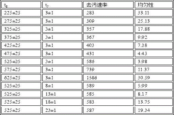
The mean temperature of the high temperature plasma jet is t g At the back side of the wafer by a temperature t y The compressed air is sprayed to reduce the temperature; by altering t g Or t y (ii) a Finally, the decontamination rate and the decontamination uniformity were measured according to the method of "decontamination characterization testSee table 2:
TABLE 2
As can be seen from Table 2, with t g The higher the stain removal rate, the greater the tendency to become, but the most stable at 525 ± 25 ℃ in view of uniformity. With t y The higher the temperature up to room temperature, the poorer the homogeneity, preferably t y =3±1℃。
In addition, it should be noted that: if the wafer 10 is directly heated, for example, the wafer 10 is heated to 200-250 deg.C t g When the temperature is not less than 225 +/-25 ℃, the decontamination rate can reach 569A/min, and the decontamination uniformity is less than 5%. However, heating the wafer 10 to 200 to 250 ℃ in a short time is more complicated for supporting equipment such as fixing and rotating the wafer, and is likely to cause great damage to the back surface of the wafer. Therefore, heating the wafer 10 to 200-250 ℃ is not recommended.
Test 7
The cleaning effect is significantly affected if the high temperature plasma jet is not confined by the capillary metal tube 28. Therefore, in the present invention, the capillary metal pipe 28 is preferably a capillary steel pipe having an inner diameter of 1 mm.
For ease of testing, the capillary metal tube 28 was replaced with a metal nozzle having an inside diameter d. The stain removal rate was measured according to the stain removal characterization test, with only the d value (in mm) changed, and is shown in table 3:
TABLE 3
| d
|
30
|
25
|
20
|
15
|
10
|
8
|
6
|
4
|
2
|
1
|
0.8
|
0.6
|
| Rate of stain removal
|
423
|
431
|
448
|
471
|
496
|
521
|
542
|
560
|
573
|
586
|
573
|
549 |
As can be seen from Table 3, d is preferably 1 mm.
The above description is only for the purpose of illustrating the preferred embodiments of the present invention and is not to be construed as limiting the invention, and any modifications, equivalents and improvements made within the spirit and principle of the present invention are intended to be included within the scope of the present invention.