CN114175229A - Bridging apparatus and method for semiconductor die transfer - Google Patents
Bridging apparatus and method for semiconductor die transfer Download PDFInfo
- Publication number
- CN114175229A CN114175229A CN202080053702.XA CN202080053702A CN114175229A CN 114175229 A CN114175229 A CN 114175229A CN 202080053702 A CN202080053702 A CN 202080053702A CN 114175229 A CN114175229 A CN 114175229A
- Authority
- CN
- China
- Prior art keywords
- substrate
- die
- bridge
- transfer
- transfer mechanism
- Prior art date
- Legal status (The legal status is an assumption and is not a legal conclusion. Google has not performed a legal analysis and makes no representation as to the accuracy of the status listed.)
- Pending
Links
Images


Classifications
-
- H—ELECTRICITY
- H01—ELECTRIC ELEMENTS
- H01L—SEMICONDUCTOR DEVICES NOT COVERED BY CLASS H10
- H01L21/00—Processes or apparatus adapted for the manufacture or treatment of semiconductor or solid state devices or of parts thereof
- H01L21/67—Apparatus specially adapted for handling semiconductor or electric solid state devices during manufacture or treatment thereof; Apparatus specially adapted for handling wafers during manufacture or treatment of semiconductor or electric solid state devices or components ; Apparatus not specifically provided for elsewhere
- H01L21/677—Apparatus specially adapted for handling semiconductor or electric solid state devices during manufacture or treatment thereof; Apparatus specially adapted for handling wafers during manufacture or treatment of semiconductor or electric solid state devices or components ; Apparatus not specifically provided for elsewhere for conveying, e.g. between different workstations
- H01L21/67703—Apparatus specially adapted for handling semiconductor or electric solid state devices during manufacture or treatment thereof; Apparatus specially adapted for handling wafers during manufacture or treatment of semiconductor or electric solid state devices or components ; Apparatus not specifically provided for elsewhere for conveying, e.g. between different workstations between different workstations
- H01L21/67715—Changing the direction of the conveying path
-
- H—ELECTRICITY
- H01—ELECTRIC ELEMENTS
- H01L—SEMICONDUCTOR DEVICES NOT COVERED BY CLASS H10
- H01L21/00—Processes or apparatus adapted for the manufacture or treatment of semiconductor or solid state devices or of parts thereof
- H01L21/67—Apparatus specially adapted for handling semiconductor or electric solid state devices during manufacture or treatment thereof; Apparatus specially adapted for handling wafers during manufacture or treatment of semiconductor or electric solid state devices or components ; Apparatus not specifically provided for elsewhere
- H01L21/67005—Apparatus not specifically provided for elsewhere
- H01L21/67011—Apparatus for manufacture or treatment
- H01L21/67144—Apparatus for mounting on conductive members, e.g. leadframes or conductors on insulating substrates
-
- H—ELECTRICITY
- H01—ELECTRIC ELEMENTS
- H01L—SEMICONDUCTOR DEVICES NOT COVERED BY CLASS H10
- H01L21/00—Processes or apparatus adapted for the manufacture or treatment of semiconductor or solid state devices or of parts thereof
- H01L21/67—Apparatus specially adapted for handling semiconductor or electric solid state devices during manufacture or treatment thereof; Apparatus specially adapted for handling wafers during manufacture or treatment of semiconductor or electric solid state devices or components ; Apparatus not specifically provided for elsewhere
- H01L21/67005—Apparatus not specifically provided for elsewhere
- H01L21/67242—Apparatus for monitoring, sorting or marking
- H01L21/67259—Position monitoring, e.g. misposition detection or presence detection
-
- H—ELECTRICITY
- H01—ELECTRIC ELEMENTS
- H01L—SEMICONDUCTOR DEVICES NOT COVERED BY CLASS H10
- H01L21/00—Processes or apparatus adapted for the manufacture or treatment of semiconductor or solid state devices or of parts thereof
- H01L21/67—Apparatus specially adapted for handling semiconductor or electric solid state devices during manufacture or treatment thereof; Apparatus specially adapted for handling wafers during manufacture or treatment of semiconductor or electric solid state devices or components ; Apparatus not specifically provided for elsewhere
- H01L21/677—Apparatus specially adapted for handling semiconductor or electric solid state devices during manufacture or treatment thereof; Apparatus specially adapted for handling wafers during manufacture or treatment of semiconductor or electric solid state devices or components ; Apparatus not specifically provided for elsewhere for conveying, e.g. between different workstations
- H01L21/67703—Apparatus specially adapted for handling semiconductor or electric solid state devices during manufacture or treatment thereof; Apparatus specially adapted for handling wafers during manufacture or treatment of semiconductor or electric solid state devices or components ; Apparatus not specifically provided for elsewhere for conveying, e.g. between different workstations between different workstations
- H01L21/67706—Mechanical details, e.g. roller, belt
-
- H—ELECTRICITY
- H01—ELECTRIC ELEMENTS
- H01L—SEMICONDUCTOR DEVICES NOT COVERED BY CLASS H10
- H01L21/00—Processes or apparatus adapted for the manufacture or treatment of semiconductor or solid state devices or of parts thereof
- H01L21/67—Apparatus specially adapted for handling semiconductor or electric solid state devices during manufacture or treatment thereof; Apparatus specially adapted for handling wafers during manufacture or treatment of semiconductor or electric solid state devices or components ; Apparatus not specifically provided for elsewhere
- H01L21/677—Apparatus specially adapted for handling semiconductor or electric solid state devices during manufacture or treatment thereof; Apparatus specially adapted for handling wafers during manufacture or treatment of semiconductor or electric solid state devices or components ; Apparatus not specifically provided for elsewhere for conveying, e.g. between different workstations
- H01L21/67703—Apparatus specially adapted for handling semiconductor or electric solid state devices during manufacture or treatment thereof; Apparatus specially adapted for handling wafers during manufacture or treatment of semiconductor or electric solid state devices or components ; Apparatus not specifically provided for elsewhere for conveying, e.g. between different workstations between different workstations
- H01L21/67721—Apparatus specially adapted for handling semiconductor or electric solid state devices during manufacture or treatment thereof; Apparatus specially adapted for handling wafers during manufacture or treatment of semiconductor or electric solid state devices or components ; Apparatus not specifically provided for elsewhere for conveying, e.g. between different workstations between different workstations the substrates to be conveyed not being semiconductor wafers or large planar substrates, e.g. chips, lead frames
-
- H—ELECTRICITY
- H01—ELECTRIC ELEMENTS
- H01L—SEMICONDUCTOR DEVICES NOT COVERED BY CLASS H10
- H01L21/00—Processes or apparatus adapted for the manufacture or treatment of semiconductor or solid state devices or of parts thereof
- H01L21/67—Apparatus specially adapted for handling semiconductor or electric solid state devices during manufacture or treatment thereof; Apparatus specially adapted for handling wafers during manufacture or treatment of semiconductor or electric solid state devices or components ; Apparatus not specifically provided for elsewhere
- H01L21/68—Apparatus specially adapted for handling semiconductor or electric solid state devices during manufacture or treatment thereof; Apparatus specially adapted for handling wafers during manufacture or treatment of semiconductor or electric solid state devices or components ; Apparatus not specifically provided for elsewhere for positioning, orientation or alignment
- H01L21/681—Apparatus specially adapted for handling semiconductor or electric solid state devices during manufacture or treatment thereof; Apparatus specially adapted for handling wafers during manufacture or treatment of semiconductor or electric solid state devices or components ; Apparatus not specifically provided for elsewhere for positioning, orientation or alignment using optical controlling means
-
- H—ELECTRICITY
- H01—ELECTRIC ELEMENTS
- H01L—SEMICONDUCTOR DEVICES NOT COVERED BY CLASS H10
- H01L21/00—Processes or apparatus adapted for the manufacture or treatment of semiconductor or solid state devices or of parts thereof
- H01L21/67—Apparatus specially adapted for handling semiconductor or electric solid state devices during manufacture or treatment thereof; Apparatus specially adapted for handling wafers during manufacture or treatment of semiconductor or electric solid state devices or components ; Apparatus not specifically provided for elsewhere
- H01L21/683—Apparatus specially adapted for handling semiconductor or electric solid state devices during manufacture or treatment thereof; Apparatus specially adapted for handling wafers during manufacture or treatment of semiconductor or electric solid state devices or components ; Apparatus not specifically provided for elsewhere for supporting or gripping
- H01L21/6835—Apparatus specially adapted for handling semiconductor or electric solid state devices during manufacture or treatment thereof; Apparatus specially adapted for handling wafers during manufacture or treatment of semiconductor or electric solid state devices or components ; Apparatus not specifically provided for elsewhere for supporting or gripping using temporarily an auxiliary support
- H01L21/6836—Wafer tapes, e.g. grinding or dicing support tapes
-
- H—ELECTRICITY
- H01—ELECTRIC ELEMENTS
- H01L—SEMICONDUCTOR DEVICES NOT COVERED BY CLASS H10
- H01L23/00—Details of semiconductor or other solid state devices
- H01L23/544—Marks applied to semiconductor devices or parts, e.g. registration marks, alignment structures, wafer maps
-
- H—ELECTRICITY
- H01—ELECTRIC ELEMENTS
- H01L—SEMICONDUCTOR DEVICES NOT COVERED BY CLASS H10
- H01L2223/00—Details relating to semiconductor or other solid state devices covered by the group H01L23/00
- H01L2223/544—Marks applied to semiconductor devices or parts
- H01L2223/5442—Marks applied to semiconductor devices or parts comprising non digital, non alphanumeric information, e.g. symbols
-
- H—ELECTRICITY
- H01—ELECTRIC ELEMENTS
- H01L—SEMICONDUCTOR DEVICES NOT COVERED BY CLASS H10
- H01L2223/00—Details relating to semiconductor or other solid state devices covered by the group H01L23/00
- H01L2223/544—Marks applied to semiconductor devices or parts
- H01L2223/54426—Marks applied to semiconductor devices or parts for alignment
-
- H—ELECTRICITY
- H01—ELECTRIC ELEMENTS
- H01L—SEMICONDUCTOR DEVICES NOT COVERED BY CLASS H10
- H01L2223/00—Details relating to semiconductor or other solid state devices covered by the group H01L23/00
- H01L2223/544—Marks applied to semiconductor devices or parts
- H01L2223/54433—Marks applied to semiconductor devices or parts containing identification or tracking information
-
- H—ELECTRICITY
- H01—ELECTRIC ELEMENTS
- H01L—SEMICONDUCTOR DEVICES NOT COVERED BY CLASS H10
- H01L2223/00—Details relating to semiconductor or other solid state devices covered by the group H01L23/00
- H01L2223/544—Marks applied to semiconductor devices or parts
- H01L2223/54473—Marks applied to semiconductor devices or parts for use after dicing
- H01L2223/54486—Located on package parts, e.g. encapsulation, leads, package substrate
Landscapes
- Engineering & Computer Science (AREA)
- Physics & Mathematics (AREA)
- Condensed Matter Physics & Semiconductors (AREA)
- General Physics & Mathematics (AREA)
- Computer Hardware Design (AREA)
- Microelectronics & Electronic Packaging (AREA)
- Power Engineering (AREA)
- Manufacturing & Machinery (AREA)
- Container, Conveyance, Adherence, Positioning, Of Wafer (AREA)
- Wire Bonding (AREA)
- Die Bonding (AREA)
Abstract
An apparatus for transferring a semiconductor die ("die") from a first substrate to a second substrate is disclosed. The apparatus includes a stage configured to hold a product substrate. The first bridge holds the transfer mechanism assembly. The second bridge holds a die substrate holder configured to hold a first substrate. The controller is configured to move the first bridge and the second bridge to align the transfer mechanism assembly with a die on the first substrate at a transfer location on the second substrate to which the die is to be transferred.
Description
Background
Semiconductor devices are electronic components that utilize semiconductor materials such as silicon, germanium, gallium arsenide, and the like. Semiconductor devices are often fabricated as a single discrete device or Integrated Circuit (IC). Examples of a single discrete device include electrically actuatable elements such as Light Emitting Diodes (LEDs), diodes, transistors, resistors, capacitors, fuses, and the like.
The manufacture of semiconductor devices typically involves a complex manufacturing process with a large number of steps. The final product of manufacture is a "packaged" semiconductor device. The "package" modifier refers to the housing and the protected features built into the final product and the interfaces that enable the devices in the package to be incorporated into the final circuit.
A conventional manufacturing process for semiconductor devices begins with processing a semiconductor wafer. The wafer is diced into a plurality of "unpackaged" semiconductor devices. The term "unpackaged" refers to unpackaged semiconductor devices that have no protected features. The unpackaged semiconductor devices may be referred to herein as semiconductor device dies, or simply "dies" for simplicity. A single semiconductor wafer may be diced to produce dies of various sizes, such that over 10 million or even 100 million dies (depending on the initial size of the semiconductor) are formed from the semiconductor wafer, and each die has a certain quality. The unpackaged die are then "packaged" via conventional manufacturing processes briefly discussed below. The action between wafer processing and packaging may be referred to as "die preparation".
In some cases, die preparation may include sorting the dies via a "pick and place process," whereby the diced dies are individually picked and sorted into bins. The classification may be based on the forward voltage capability of the die, the average power of the die, and/or the wavelength of the die.
Typically, packaging involves mounting the die into a plastic or ceramic package (e.g., a mold or housing). The package also includes connecting the die contacts to pins/wires to interface/interconnect with the final circuit. Packaging of semiconductor devices is typically accomplished by encapsulating the die to protect it from the environment (e.g., dust).
The product manufacturer then places the packaged semiconductor device into a product circuit. Due to the encapsulation, the device can be "plugged" into the circuit assembly of the product being manufactured at any time. Furthermore, while the packaging of the device may protect the device from elements that may degrade or damage the device, the packaged device is inherently larger than the die present within the package (e.g., in some cases, the packaged device is approximately 10 times thicker than the die, 10 times larger in area, and thus 100 times larger in volume). Therefore, the resulting circuit assembly cannot be thinner than the package of the semiconductor device.
Drawings
The detailed description explains with reference to the drawings. In these figures, the left-most digit(s) of a reference number identifies the figure in which the reference number first appears. The use of the same reference symbols in different drawings indicates similar or identical items. Further, the drawings may be considered to provide approximate depictions of the relative dimensions of various components in the various figures. However, the drawings are not to scale and the relative sizes of various components within each drawing and between different drawings may differ from that depicted. In particular, for clarity, some drawings may depict components as being of a certain size or shape, while other drawings may depict the same components as being of a larger scale or in a different shape.
Fig. 1 shows a schematic diagram of an embodiment of elements of a die transfer system.
Fig. 2 shows a schematic view of an exemplary transfer device for transferring dies from a die substrate to a product substrate, the transfer device having a bridging device, according to an embodiment of the present application.
Fig. 3 shows a schematic view of an example transfer device for transferring die from a die substrate to a product substrate having a plurality of transfer mechanism assemblies on a first bridge member and a plurality of die substrates on a second bridge member according to an embodiment of the present application.
Fig. 4 shows a schematic view of an example transfer device for transferring dies from a die substrate to a product substrate, the transfer device having more than two bridging devices, according to an embodiment of the present application.
Figure 5 illustrates a plan view of an embodiment of a product substrate having circuit traces thereon according to an embodiment of the present application.
Fig. 6 illustrates a method of a die transfer operation according to an embodiment of the present application.
Fig. 7 illustrates a method of a die transfer operation according to an embodiment of the present application.
Fig. 8 illustrates a method of a die transfer process according to an embodiment of the present application starting with a die substrate held by a first bridge and a transfer mechanism assembly held by a second bridge.
Fig. 9 illustrates a method for determining a location for a die transfer process based at least in part on one or more parameter criteria and/or optimizations, according to an embodiment of the application.
Detailed Description
The present disclosure relates to a machine for directly transferring and adhering a semiconductor device die to a circuit and a process for implementing the same, and to a circuit (as an output product) having a die adhered thereto. In an embodiment, the machine is used to transfer unpackaged dies directly from a substrate (such as "wafer tape") to a product substrate (such as a circuit substrate). Direct transfer of the unpackaged die may significantly reduce the thickness of the finished product and reduce the time and/or cost for manufacturing the product substrate as compared to similar products produced by conventional means.
For purposes of this specification, the term "substrate" refers to any substance on or against which a process or action takes place. Further, the term "product" refers to a desired output from a process or action, regardless of completion status. Thus, a product substrate refers to any substance on or for which a process or action occurs to achieve a desired output. Herein, the term "product substrate" may include, but is not limited to: wafer tape (e.g., for pre-sorting die and producing sorted die slices for future use); a paper or polymer substrate formed into a sheet or other non-planar shape, wherein the polymer (translucent or otherwise) may be selected from any suitable polymer, including but not limited to silicone, acrylic, polyester, polycarbonate, and the like; a circuit board (such as a Printed Circuit Board (PCB)); a string or line circuit, which may include a pair of conductive wires or "threads" extending in parallel; and cotton, nylon, rayon, leather, and other fabrics. The material selection for the product substrate may include durable, flexible, rigid, and other materials that enable the transfer process to be successful and maintain the end-use suitability of the product substrate. The product substrate may be formed solely or at least partially of an electrically conductive material such that the product substrate acts as an electrically conductive circuit for forming the product. Potential types of product substrates may also include articles such as glass bottles, vehicle windows, or glass sheets.
In one embodiment, the product substrate may include circuit traces disposed thereon. As depicted, the circuit traces may include a pair of adjacent traces separated by a trace spacing or gap to accommodate the distance between electrical contact terminals (not shown) on the die being transferred. Thus, the trace spacing or gap between adjacent ones of the circuit traces may be sized according to the size of the die being transferred to ensure proper connectivity and subsequent die activation. For example, the circuit traces may have trace spacings or gaps ranging from about 10 to 200 microns, about 100 to 175 microns, or about 125 to 150 microns.
The circuit traces may be formed from conductive ink that is disposed via screen printing, ink jet printing, laser printing, hand printing, or other printing means. In addition, the circuit traces may be pre-cured and semi-dried or dried to provide additional stability while also enabling activation of the circuit traces for purposes of die conductivity. Wet conductive ink may also be used to form the circuit traces, or a combination of wet and dry ink may be used to form the circuit traces. Alternatively or additionally, the circuit traces may be pre-formed as wire traces, or photo-etched, or formed from a molten material into a circuit pattern and then adhered, embedded, or otherwise secured to the product substrate.
The material of the circuit traces may include, but is not limited to, silver, copper, gold, carbon, conductive polymers, and the like. In one embodiment, the circuit traces may include silver coated copper particles. The thickness of the circuit traces may vary depending on the type of material used, the intended function, and the appropriate strength or flexibility to achieve that function, the energy capacity, the size of the LED, etc. For example, the thickness of the circuit traces may range from about 5 to 20 microns, from about 7 to 15 microns, or from about 10 to 12 microns.
Thus, in one non-limiting example, the product substrate may be a flexible, translucent polyester sheet having a desired circuit pattern screen printed thereon using a silver-based conductive ink material to form circuit traces.
In one embodiment, the machine may hold the product substrate to receive "unpackaged" dies (such as LEDs), for example, transferred from a wafer tape. To reduce the size of the product in which the die is used, the die can be very small and thin. For example, the die may be about 50 microns thick. In other cases, the thickness of the die may be less than 30 microns. It should be noted, however, that the systems and methods as disclosed herein may be applied to die thicknesses greater than 50 microns, such as 200 microns or greater. Because of the relatively small size of the die, the machine includes features for precisely aligning both the wafer tape carrying the die and the transfer mechanism with the transfer locations on the product substrate to ensure accurate placement and/or avoid waste of product material. In one embodiment, the means for aligning the transfer mechanism and the die on the wafer tape may include a set of bridges to which the wafer tape and the transfer mechanism are respectively secured and individually transported to an alignment position such that a particular die on the wafer tape is transferred to a particular site on the product substrate.
In one embodiment, the machine further includes a transfer mechanism for transferring the die from the wafer tape directly to the product substrate without "packaging" the die. The transfer mechanism may be disposed vertically above the wafer tape so as to press down on the die through the wafer tape toward the product substrate. This pressing down on the die may cause the die to peel away from the wafer tape, starting at the side of the die until the die is separated from the wafer tape for attachment to a product substrate. That is, the die may be transferred by reducing the adhesion between the die and the wafer tape and increasing the adhesion between the die and the product substrate.
In one embodiment, the transfer mechanism may include an elongated rod, such as a prong or a pin, that may be periodically actuated against the wafer tape to push the wafer tape from the top side. The pins may be sized to not exceed the width of the transferred die. In other cases, however, the width of the pin may be wider than the width of the die, or any other dimension. When the ends of the pins contact the wafer tape, the wafer tape may experience local flexing in the area between the die and the wafer tape. Because the flexing is highly localized and progresses rapidly, portions of the wafer tape that do not receive pressure from the pins may begin to bend away from the surface of the die. Thus, the partial separation may cause the die to lose sufficient contact with the wafer tape to become detached from the wafer tape. Further, in one embodiment, the flexing of the wafer tape may be minimal to maintain the entire surface area of the die in contact with the wafer tape while still allowing the opposing surfaces of the die to extend beyond the extended surfaces of the corresponding surfaces of the adjacent die to avoid inadvertent transfer of the adjacent die.
In one embodiment, the transfer device may include one or more bridging structures for holding a frame carrying the die substrate and the transfer mechanism assembly. Similar to other embodiments described herein, the die substrate may be a wafer tape with semiconductor die attached. The transfer mechanism assembly may include a pin actuator configured to actuate a pin that, when aligned, presses a die from a die substrate onto a product substrate. In some cases, the product substrate may be disposed on a stage configured to translate the product substrate in a first direction. The one or more bridging structures may also be configured to move in substantially the same first direction and thus move the core substrate and/or the transfer mechanism assembly in that direction. In other words, the stage on which the product substrate is located may be movably disposed in the transfer device and may be configured to be moved manually and/or via a computer-controlled motor. Similarly, the one or more bridging structures may be movably mounted on a set of rails of the transfer device, and may also be configured to move via computer-controlled motors.
Each bridge may have a rail or track provided thereon that extends substantially perpendicular to the set of rails on which the bridging structure is mounted. The transfer mechanism assembly and the frame carrying the die substrate may be mounted to the same bridge or each to a different bridge via the above-mentioned guide rails or tracks, such that the frame carrying the die substrate and/or the transfer mechanism assembly is movable in a second direction, which is substantially perpendicular to the first direction in which the bridge structure is movable. In this way, the bridge structure may be moved in the first direction independent of movement of the frame carrying the die substrate and/or the transfer mechanism assembly in the second direction.
The one or more bridge structures, the frame carrying the die substrate, the transfer mechanism assembly, and/or the product substrate may be moved via computer-controlled motors such that the transfer mechanism assembly is aligned with a next die to be transferred on the die substrate and a next transfer location on the product substrate. At this point, the pins of the transfer mechanism assembly may be actuated to apply pressure to the die substrate on the back side of the next die to be transferred, bringing the die into contact with the product substrate at the location on the product substrate where the die is to be placed and transferring to the product substrate. This process may be repeated until all of the dies to be transferred onto the product substrate have been transferred from the die substrate (e.g., wafer tape) onto the product substrate.
In one embodiment, the transfer device can have a first bridge and a second bridge ("bridge"). Both the first and second bridges may be movable in a first direction (e.g., along a length or width of the product substrate) along first and second rails ("rails"), wherein the first and second rails may be disposed on opposite sides of a stage configured to hold the product substrate, respectively. Although the term "guide rail" is used for purposes of this specification, it should be understood that any guide suitable for movement of the bridge substantially in a single direction (e.g., in the first direction but not in a direction having a component orthogonal to the first direction) is contemplated according to one embodiment. The bridge may have one or more motors respectively disposed thereon to move the bridge along the guide rails. Additionally, the bridge may be mechanically coupled to one or more motors, such as by way of cables, chains, and/or pulleys, so as to be movable along the guide rails.
The first bridge may include two legs engaged with the first rail and the second rail, respectively, and a bridge connected between the two legs. The bridge spans the stage and/or a product substrate disposed on the stage. The bridge portion of the first bridge may have a track or guide disposed along a portion of its length. The track may extend along the bridge in a direction substantially perpendicular to the first and second rails to which the first bridge may be movably mounted. The transfer mechanism assembly may be movably disposed along the track. The transfer mechanism assembly may be mechanically coupled to one or more computer-controlled motors to move the transfer mechanism assembly along the track of the first bridge. In one embodiment, the transfer mechanism assembly may be disposed on a track such that the transfer mechanism assembly may be configured to move across the entire distance (e.g., width) of the stage and/or the product substrate disposed on the stage.
Similar to the first bridge, the second bridge may further include two legs engaged with the first rail and the second rail, respectively, and a bridge connected between the two legs. The bridge spans the stage and/or a product substrate disposed on the stage. The bridge portion of the second bridge may also have a track or guide disposed along a portion of its length. The track may extend along the bridge in a direction substantially perpendicular to the first and second rails to which the second bridge may be movably mounted. The die substrate mounted on the frame or the holder may be movably disposed along the rail of the second bridge. The die substrate may be mechanically coupled to one or more computer-controlled motors to move the die substrate mounted on the die substrate frame along the rails of the second bridge. In one embodiment, the die substrate frame may be disposed on a track such that the die substrate may be configured to move across the entire distance (e.g., width) of the stage and/or the product substrate disposed on the stage.
The two bridge members, as well as the stage, transfer mechanism assembly, and die substrate, may be moved via the controller to align the die to be transferred on the die substrate and the pins of the transfer mechanism assembly with the locations on the product substrate where the die is to be placed. After alignment, the pins of the transfer mechanism assembly may be actuated to push the die into contact with the product substrate (or circuit traces on the product substrate, as appropriate) to transfer the die onto the product substrate.
According to one embodiment, the transfer device may include more than one transfer mechanism assembly and more than one die substrate located on each of the two bridge structures. This may allow parallel processing of the dies transferred to the product substrate (e.g., small movements of the part followed by die transfer). A transfer device having multiple transfer mechanism assemblies and multiple corresponding die substrates may allow for assembly using different types of dies. For example, a particular color of micro-LED may be transferred from a first die substrate, while a different color of micro-LED may be transferred from another die substrate. In another example, the lens or electrically actuated element (i.e., capacitor, transistor, controller, etc.) may be transferred from the first substrate, while LEDs of any size or color may be transferred from the second substrate.
In one embodiment, the transfer device may include fewer or more than two bridging structures (e.g., one, three, four, five, etc.). For example, four bridge structures may be implemented, wherein two sets of two bridge structures may be configured to operate in parallel to increase throughput of the product substrates output by the transfer device. As described above, diversity may also be achieved using multiple sets of transfer mechanism assemblies and die substrate holders by transferring one type of lens or other electrically actuated element from one set of bridging structures and another type of lens or other electrically actuated element from another set of bridging structures. It should also be understood that in any embodiment, a single bridge structure may implement both the transfer mechanism assembly and the die substrate holders, or in the case of at least two bridge structures, one or more transfer mechanism assemblies and one or more die substrate holders may be distributed separately over adjacent bridge structures of the transfer device (i.e., the transfer mechanism assembly on a first bridge works with the die substrate holders on adjacent bridges) such that the bridge structures move together to transfer the dies.
In one embodiment, one or more sensors may be implemented to assist the transfer device in determining the precise transfer position and alignment of the components involved in the transfer. Further, a die map may be used to help guide the apparatus in determining which die on a given die substrate should be transferred based on die quality or other die factors. The implementation of the sensor and die map is similar to that discussed in us patent 9,633,883.
Die transfer rates using the transfer devices described herein in conjunction with the multiple transfer mechanisms discussed in U.S. application 15/978,094 may achieve significantly higher transfer rates than are available in conventional machines. The die transfer rate is the number of dies transferred per second by the device, for example, the rate may be in the range of about 5 to 500 dies, 50 to 400 dies, 100 to 300 dies, or 150 to 250 dies placed per second.
Fig. 1 shows a simplified example of an embodiment of a direct transfer system 100. The transfer system 100 may include a Personal Computer (PC)102 (or server, data input device, user interface, etc.), data storage 104, a wafer tape mechanism 106, a product substrate mechanism 108, and a transfer mechanism 110. Since the wafer tape mechanism 106, the product substrate mechanism 108, and the transfer mechanism 110 have been described in greater detail so far, specific details regarding these mechanisms will not be repeated here. However, how the wafer tape mechanism 106, the product substrate mechanism 108, the transfer mechanism 110 relate to the interaction between the PC 102 and the data storage device 104 will be briefly described below.
In one embodiment, PC 102 communicates with data storage device 104 to receive information and data useful in a transfer process that uses transfer mechanism 110 to transfer dies from wafer tape in wafer tape mechanism 106 directly onto product substrates in product substrate mechanism 108, where the dies may be attached to the product substrates. The PC 102 may also serve as a receiver, compiler, organizer, and controller for data relayed to each of the wafer tape mechanism 106, the product substrate mechanism 108, and the transfer mechanism 110. PC 102 may also receive orientation information from a user of transfer system 100. Note that although fig. 1 depicts directional motion capability arrows adjacent the wafer tape mechanism 106 and the product substrate mechanism 108, these arrows merely indicate general mobility directions, it is contemplated that both the wafer tape mechanism 106 and the product substrate mechanism 108 can also be configured to move in other directions, including, for example, rotation in a plane, pitch, roll, and yaw.
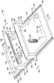
Fig. 2 shows a schematic view of an exemplary transfer device 200 for transferring a die 272 from a die substrate 270 to a product substrate 210, the transfer device having bridging devices 230, 260. The transfer device 200 may include a movable stage 202 configured to hold a product substrate 210. The moveable stage 202 may be configured to move in one or more directions (e.g., an x-direction, a y-direction, or both an x-and y-direction). In one embodiment, the moveable stage 202 may also be configured to move up and down (e.g., in the z-direction). For example, movable stage 202 may be configured to move in direction 222 by being coupled to a motor or other mechanical device.
The product substrate 210 may be any suitable material as described herein (e.g., PCB, FR-4 board, paper, cardboard, glass, ceramic, plastic, tape, etc.). The product substrate 210 may have previously transferred dies 212, such as semiconductor dies, and/or circuit traces 214 disposed and/or formed thereon and/or therein. In one embodiment, the die 212 may be disposed on the product substrate 210 according to the methods and apparatus described herein. The circuit traces 214 may be of any suitable type and/or areal density. These circuit traces 214 may be conductive and configured to carry electrical current, such as between the die 212 and one or more other elements of the product substrate 210.
The product substrate 210 may also include any suitable type of alignment features 216, 218, such as a tree structure 216 or a reticle 218. The alignment features 216, 218 may have known coordinates for a particular product substrate 210 that may be recognized by a controller, such as the PC 102. The alignment features 216, 218 and their known coordinates may be used by the PC 102 to determine the position of various components of the transfer device 200. Accordingly, the alignment structures 216, 218 may be detected, such as by optical imaging detection, and used to align and/or orient the components of the transfer device 200 to transfer the die 272 onto the product substrate 210. The product substrate 210 may also have locations and/or positions 220 to which the dies are to be transferred. In some cases, the location 220 to which the die is to be transferred may be visually identifiable and may be identified by optical detection. Such visual indicia of the locations 220 to which the dies are to be transferred may also be used to align components of the transfer device 200 to transfer the dies 272 onto the product substrate 210. The PC 102 may receive information about the product substrate 210, such as the die transfer locations 220 and/or the alignment features 216, 218, in the form of a product substrate data file.
The transfer device 200 may also include a first bridging structure 230 and a second bridging structure 260. The first bridge structure 230 may have a first leg 232, a second leg 234, and a bridge 236 disposed between the first and second legs 232, 234. The first bridge structure 230 may be configured to move along the first rail 290 and the second rail 292. The legs 232, 234 may be movably coupled to the rails 290, 292 to allow the first bridge structure 230 to move along the first rail 290 and the second rail 292.
The first bridge structure 230 may have rails and/or tracks 238 disposed along its bridge portion 236. The transfer mechanism assembly 240 may be movably mounted on the track 238 as described herein. The range of positions of the rails 238, and thus the transfer mechanism assembly 240, may be equal to or greater than the width of the product substrate 210 to enable the die 272 to be transferred to any suitable location on the product substrate 210. As described herein, transfer mechanism assembly 240 may have prongs 276 that may be actuated to extend outwardly from transfer mechanism assembly 240 and retract inwardly toward transfer mechanism assembly 240.
The first bridge structure 230 may also include one or more motors 242, 244, 246, 248 to enable the first bridge structure 230 to move along the rails 290, 292 and the transfer mechanism assembly 240 to move along the track 238. The motor 242 may be enclosed within the second leg 234, such as within a housing of the second leg 234, and the motor 244 may be enclosed within the first leg 234. The motors 242, 244 may be controlled by a computer (such as by the PC 102) to exert a force on the legs 232, 234 relative to the rails 290, 292 to move the first bridge structure along the rails 290, 292 in the direction 252. Direction 252 may be the same direction as direction 222 (along which moveable stage 202 may be configured to move).
Although the motors are depicted as being disposed on the legs 232, 234, it should be understood that any suitable coupling of the motors 242, 244 with the legs 232, 234 may be implemented to move the first bridge structure 230 along the rails 290, 292. For example, each leg 232, 234 of the first bridge structure 230 may have more than one motor 242, 244. Additionally, in one embodiment, the motors 242, 244 may be located outside of the legs 232, 234 and coupled to each leg separately via wires, cables, pulleys, and the like.
It should be understood that a controller, such as PC 102, may receive signals from sensor 250, camera 298, and/or any other suitable detector and position first bridging structure 230 in a desired location. The positioning may correspond to the next die 272 to be transferred onto the product substrate 210. Further, PC 102 may be configured to position transfer mechanism assembly 240 along track 238 of first bridging structure 230. Specifically, PC 102 may control one or more motors 242, 244, 246, 248 to position first bridging structure 230 and transfer mechanism assembly 240. As discussed herein, such positioning may also be based at least in part on one or more data files, such as data files indicating locations of dies to be placed on the product substrate 210, and/or data files indicating locations of dies and/or known good dies on the die substrate 270.
In one embodiment, the second bridging structure 260 may be substantially similar to the first bridging structure 230. The second bridge structure 260 may have a first leg 262, a second leg 264, and a bridge 266 disposed between the first and second legs 262, 264. The second bridge structure 260 may be configured to move along the first rail 290 and the second rail 292. The legs 262, 264 may be movably coupled to the rails 290, 292 and may allow the second bridge structure 260 to move along the first rail 290 and the second rail 292. Since both the first bridge structure 230 and the second bridge structure 260 are coupled to the same guide rails 290, 292, movement of the first bridge structure 230 may be limited by the position of the second bridge structure 260 along the guide rails 290, 292, and vice versa. The second bridge structure may be moved in the same direction 282 as the direction of movement 252 of the first bridge structure 230. In other words, the movement of both the first bridge structure 230 and the second bridge structure 260 may be in the same direction (e.g., the x-direction).
In one embodiment, the movement of the first bridge structure 230 and the second bridge structure 260 may span substantially the entire length of the moveable stage 202 and/or the product substrate 210. This allows the first bridge structure 230 and the second bridge structure 260 to cooperate to place the die 272 on substantially the entire surface of the product substrate 210.
The second bridge structure 260 may have a track (obscured in this view) disposed along its bridge portion 266. A die substrate frame 268 (on which a die substrate 270 with an unpackaged die 272 is held) may be movably mounted on rails of the second bridge structure 260. The range of positions of the rails, and thus the die substrate 270, may be equal to or greater than the width of the product substrate 210 to enable the transfer of the die 272 to any suitable location on the product substrate 210. As described herein, the die substrate 270 may be any suitable substrate, such as a wafer tape, on which the unpackaged die 272 to be transferred to the package substrate 210 is held.
The second bridge structure 260 may also include one or more motors 278, 280, 284, 286 to enable the second bridge structure 260 to move along the rails 290, 292 and/or to enable the die substrate 270 to move along the rails of the second bridge structure 260. The motor 278 may be enclosed within the first leg 262, such as within a housing of the first leg 262, and the motor 280 may be enclosed within the second leg 264. The motors 278, 280 may be controlled by a computer (e.g., via the PC 102) to exert a force on the legs 262, 264 relative to the rails 290, 292 to move the second bridge structure 260 in the direction 282 along the rails 290, 292. In some cases, direction 282 may be along direction 222 along which moveable stage 202 may be configured to move, and also along direction 252 along which first bridging structure 230 is configured to move.
As with the first bridge structure 230, although the motors 278, 280 are depicted as being disposed in the legs 262, 264, it should be appreciated that any suitable configuration of the motors 278, 280 relative to the legs 262, 264 may be used to move the second bridge structure 260 along the rails 290, 292. For example, each leg 262, 264 of the second bridge structure 260 may have more than one motor 278, 280. Further, in some cases, the motors 278, 280 may be disposed outside of the legs 262, 264 and coupled to the legs 262, 264, such as by wires, cables, pulleys, and the like.
The motors 284, 286 can be disposed in and/or on the bridge portion 266 of the second bridge structure 260. The die substrate 270 may be mechanically coupled to the motors 284, 286 by wires, cables, pulleys, etc. (not shown). With the die substrate frame 268 having the die substrate 270 mounted thereon, the motors 278, 280 may be controlled via the PC 102 to move the die substrate 270 along the length of the track of the second bridge structure 260. The second bridging structure 260 may also include one or more sensors 274, depicted here as linear sensors 274. The sensor 274 may be substantially similar to the sensor 250 and may be configured to provide a signal to the PC 102 indicating the position of the die substrate frame 268 and the die substrate 270 along the length of the bridge 266.
Although the guide rails 290, 292 are depicted herein as housings having grooves 294, 296 therein, the guide rails 290, 292 may be of any suitable type. In fact, any suitable guide, rail, track, or other device may be used for the movement of the first bridge structure 230 and/or the second bridge structure 260. The transfer device 200 may also include a camera 298 as discussed herein. Signals, such as image signals, may be processed by the PC 102 and used in some cases in conjunction with signals from the sensors 250, 274 to control movement of the bridge structures 230, 260, the transfer mechanism assembly 240, and/or the die substrate 270.
Under the controller of the PC 102, the first bridge structure 230 and the second bridge structure may move with the transfer mechanism assembly 240 and the die substrate 270 to align the die 272 to be transferred with the pins 276 and the locations 220 on the product substrate where the die 272 is to be placed. The PC 102 may perform this alignment by controlling one or more motors 242, 244, 278, 280, 246, 248, 284, 286 or other suitable electromechanical devices.
It should be understood that under the control of the controller and based at least in part on the information about the product substrate 210 and the information about the die substrate 270, the die 272 may be aligned with the pins 276 of the transfer mechanism assembly 240 and with the locations on the product substrate to which the die 272 will be transferred. When these elements are aligned in two directions (e.g., x and y directions), the prongs 276 may be actuated under the control of a controller (e.g., PC 102) to push the die 272 in a third direction (e.g., z direction) into contact with the location on the product substrate 210 to which the die 272 will be transferred. The actual occurrence of the transfer may be achieved when the adhesion between the die and the substrate to which the die is to be transferred becomes greater than the adhesion between the die and the substrate to which the die is to be transferred.
It should be appreciated that the product substrate 210, and thus the stage 202, may have any suitable dimensions to accommodate the production of current and next generation products. For example, the die 272 (e.g., LEDs, micro-LEDs, ICs, electrically actuated elements, etc.) may be attached to substrates having a relatively small area, such as those used for smart watch PCBs and smart watch displays, or to Gen 10.5 and above glass substrates that are, for example, 3.3 meters by 2.9 meters in size. In fact, the size of the transfer device 200 may be scaled to optimize for the product being manufactured thereon.
It should be understood that there may be a set of locations that may align die 272, pins 276, and locations 220 on product substrate 220. In practice, there are multiple movable elements (e.g., the movable stage 202, the first bridge structure 230, the second bridge structure 260, the transfer mechanism assembly 240, the die substrate 270, etc.) that may allow one region (in the x and y directions) to be selected for transfer. This transfer point may be referred to as an alignment point and, with reference to the initial reference frame, corresponding coordinates on the stage reference frame and/or the bridge reference frame may be determined from this alignment point. Thus, the alignment point may be a point in a fixed reference frame where the product substrate 210, the pins 276, and the die 272 are to be aligned. Since the location of the alignment point can be selected, various algorithms can be used to determine the alignment point for a particular die transfer process. The alignment point may be determined based at least in part on one or more parameters, such as misalignment level and/or transfer time, which may be optimized or thresholded.
Fig. 3 shows a schematic diagram of an exemplary transfer device 300 for transferring die 372 from die substrates 370, 371 to product substrate 310 having a plurality of transfer mechanism assemblies 332, 334 on a first bridge 330 and a plurality of die substrates 342, 344 on a second bridge 340. Each of the plurality of transfer mechanism assemblies 332, 334 includes a respective pin 376, 377. The transfer device 300 may be similar to the transfer device 200 of fig. 2. There may be features and/or variations between the transfer device 300 and the transfer device 400 (fig. 4) that may be implemented in another exemplary transfer device embodiment. In other words, the disclosure herein contemplates any combination of the features discussed in connection with the transfer device 200 and the transfer device 300.
Similar to the transfer device 200, the transfer device 300 may include a movable stage 302. As shown, the moveable stage 302 may be moveable in a first direction and a second direction substantially perpendicular to the first direction (e.g., in the x-direction and y-direction 312). In other words, the moveable stage 302 may be controlled in both directions via motors and/or other electromechanical devices. In addition, the movable stage 302 may be configured to move in only one direction, similar to the movable stage 202 of the transfer device 200 of fig. 2. Regardless of the freedom of movement of the moveable stage 302, a product substrate 310, which is substantially similar to the product substrate 210 of fig. 2, may be supported on the moveable stage 302.
The transfer device 300 may have a first bridging structure 330 and a second bridging structure 340, which may be substantially similar to the first bridging structure 230 and the second bridging structure 260 of fig. 2, and for brevity, will not be described again. For a more simplified drawing, the motors and certain other elements used to move the first and second bridging structures 330, 340 and the elements attached thereto are not shown, as they are shown in fig. 2, but it should be understood that they are present.
The first bridging structure 330 may movably retain a first transfer mechanism assembly 332 and a second transfer mechanism assembly 334. Similarly, the second bridge structure 340 may movably hold a first die substrate frame 342 and a second die substrate frame 344. Having two transfer mechanism assemblies 332, 334 and two die substrate frames 342, 344 on the first bridge structure 330 may allow parallel processing (e.g., small movements of the components followed by die transfer) of the dies transferred onto the product substrate 310. In one embodiment, this configuration with multiple transfer mechanism assemblies 332, 334 on the first bridge structure 330 and multiple corresponding die substrate frames 342, 344 on the second bridge structure 340 may allow for die transfer with different types of dies. For example, a particular color of micro-LED may be transferred from a first die substrate, while a different color of micro-LED may be transferred from another die substrate.
Fig. 4 shows a schematic view of an exemplary transfer device 400 for transferring dies from more than one die substrate frame 442, 452 to a product substrate 410, the transfer device having more than two bridging devices 430, 440, 450, 460. Similar to the transfer device 200, the transfer device 400 may include a movable stage 402 configured to hold a product substrate 410 thereon. The movable stage may be configured to move in a single direction 412 (as shown), or alternatively in two directions (e.g., x-direction and y-direction).
The transfer device 400 may have a first bridging structure 430 and a second bridging structure 440, and a third bridging structure 450 and a fourth bridging structure 460, which may be substantially similar to the first bridging structure 230 and the second bridging structure 260 of fig. 2, and therefore, for brevity, will not be described again. For a more simplified drawing, the motors and certain other elements for moving the bridging structures 430, 440, 450, 460 and the elements attached thereto are not shown, as they are shown in fig. 2, but it should be understood that they are present.
The first bridge structure 430 may movably hold the first transfer mechanism assembly 432 and the second bridge structure 440 may movably hold the first die substrate frame 442. Similarly, the third bridge structure 450 may movably hold a second die substrate frame 452, and the fourth bridge structure 460 may movably hold a second transfer mechanism assembly 462. Each of the first and second transfer mechanism assemblies 432, 462 includes a respective pin 476 (the pin of the first transfer mechanism assembly 432 is obscured by the fourth bridging structure 460). The plurality of transfer mechanism assemblies 432, 462 are associated with transfers for transferring the die 472 from the die substrates 470, 471 to the product substrate 410.
The bridging structures 430, 440, 450, 460 may be configured to operate in parallel to increase the throughput of the product assembled by the transfer device 400. In one embodiment, the configuration may also achieve die diversity by transferring one type of die from one set of bridging structures 430, 440 and another type of die from another set of bridging structures 450, 460. It should also be understood that embodiments may include more than two bridge structures, as well as more than one transfer mechanism assembly and/or die substrate movably coupled to one or more bridge structures of a transfer device.
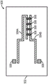
Fig. 5 shows an embodiment of a treated product substrate 500. The product substrate 502 may include a first portion of circuit traces 504A that may function as either negative or positive power terminals when power is supplied thereto. A second portion of circuit trace 504B may extend adjacent to the first portion of circuit trace 504A and may serve as a corresponding positive or negative power supply terminal when power is supplied thereto.
As similarly described above with respect to wafer tape, to determine where to convey the product substrate 502 to perform the transfer operation, the product substrate 502 may have a barcode (not shown) or other identifier that is read or otherwise detected. The identifier may provide circuit trace data to the device. The product substrate 502 may also include fiducials 506. The fiducial 506 may be a visual indicator for sensing to locate the first portion 504A and the second portion 504B of the circuit trace. Once the fiducial 506 is sensed, the shape and relative position of the first portion 504A and the second portion 504B of the circuit trace with respect to the fiducial 506 may be determined based on pre-programmed information.
Additionally, die 508 is depicted in fig. 5 as spanning between first portion 504A and second portion 504B of circuit traces. In this manner, electrical contact terminals (not shown) of the die 508 may be bonded to the product substrate 502 during a transfer operation, such as by the transfer devices 200, 300, 400. Accordingly, power may be applied to energize between the first portion 504A and the second portion 504B of the circuit traces to power the die 508. For example, the dies may be unpackaged LEDs that have been transferred from the wafer tape directly to circuit traces on the product substrate 502. Thereafter, the product substrate 502 may be processed to complete the product substrate 502 and used in a circuit or other finished product. Further, other components of the circuit may be added by the same or other transfer mechanisms to create a complete circuit, and control logic may be included to control the LEDs as one or more groups in some static or programmable or adaptive manner.
Fig. 6 illustrates a method 600 of performing a direct transfer process in which one or more dies are transferred directly from a die substrate (such as a wafer tape) to a product substrate. The processes of method 600 described herein may be performed out of any particular order and thus may be performed in any satisfactory order to achieve a desired product state. The method 600 may include the step 602 of loading the transfer process data into the PC 102 and/or data storage device. The transfer process data may include data such as die map data, circuit CAD file data, and/or pin profile data.
The method 600 may also include an operation 604 of loading a wafer tape onto the wafer tape frame mechanism. Loading the wafer tape into a wafer tape frame, such as die substrate frames 268, 342, 344, 442, 452, may include controlling movement of the die frames to a loading position. In other embodiments, loading the wafer tape into the wafer tape frame may not require moving the wafer tape frame to the loading position. A wafer tape (such as die substrate 270) may be secured in the wafer tape frame mechanism in a loading position. The wafer tape may be loaded such that the dies of the semiconductor (such as die 272) face down toward the product substrate transport mechanism.
The method 600 may also include a step 606 of preparing the product substrate for loading into a product substrate stage. Preparing the product substrate may include the step of screen printing circuit traces on the product substrate according to the pattern of a CAD file loaded into a PC or data storage device. In addition, fiducial marks may be printed on the circuit substrate to aid in the transfer process. A product substrate stage, such as stage 202, may be controlled to move to a loading position where a product substrate, such as product substrate 210, may be loaded into the product substrate stage. The product substrate may be loaded such that the circuit traces face the dies on the wafer. For example, in one embodiment, the product substrates may be delivered and placed in the loading position by a conveyor (not shown) or other automated mechanism, such as in the form of an assembly line. Alternatively, the product substrate may be loaded manually by an operator.
Once the product substrate is properly loaded onto the movable stage and the wafer tape is properly loaded into the wafer tape frame, a program for controlling the direct transfer of dies from the wafer tape to the circuit traces of the product substrate may be executed via PC 102 to initiate direct transfer operation 608. Details of this direct transfer operation are described herein.
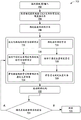
Fig. 7 illustrates a method 700 of a direct transfer operation that causes dies to be transferred directly from a wafer tape (or other substrate holding dies, also referred to as a "die substrate" for the simplified description of fig. 7) to a product substrate. The operations of method 700 described herein may be performed out of any particular order and thus may be performed in any satisfactory order to achieve a desired product state.
To determine which die is to be placed on the product substrate and where the die is to be placed on the product substrate, PC 102 may receive input 702 regarding the identity of the product substrate and the identity of the die substrate containing the die to be transferred. This input may be manually entered by a user or PC 102 may send a request to a cell manager that controls the product substrate alignment sensor and the die detector, respectively. The request may instruct the sensor to scan an identifying indicia, such as a barcode or QR code, on the loaded substrate, and/or the request may instruct the detector to scan an identifying indicia, such as a barcode or QR code, on the loaded die substrate.
In performing the process of transferring the die to the product substrate, PC 102 can determine an initial orientation 706 of the product substrate and the die substrate relative to the transfer mechanism and the holding mechanism. In process 706, PC 102 can instruct the substrate alignment sensor to locate a fiducial point on the product substrate. As discussed above, the fiducial points may be used as reference marks for determining the relative position and orientation of circuit traces on the product substrate. Further, PC 102 may instruct the die detector to position one or more reference points on the die substrate to determine the placement of the die.
Once the initial orientation of the product substrate and the die substrate is determined, PC 102 can instruct the respective product substrate and die substrate transport mechanisms to orient the product substrate and the die substrate to a position aligned with the transfer mechanism and the securing mechanism, respectively 708.
The alignment step 708 may include determining a location 710 of a portion of the circuit trace to which the die is to be transferred and a location 712 at which the portion is located relative to the transfer fixture location. The transfer fixture position may be considered as an alignment point between the transfer mechanism and the product substrate. Based on the data determined in steps 710 and 712, PC 102 can instruct the product substrate transport mechanism to transport the product substrate so as to align the portion of the circuit traces to which the die is to be transferred with transfer fixture location 714.
The alignment step 708 may also include determining which die on the die substrate is to be transferred 716 and where the die is located relative to the transfer fixture location 718. Based on the data determined in steps 716 and 718, PC 102 can instruct the wafer tape transport mechanism to transport the die substrate so that the die to be transported is aligned 720 with the transfer fixture location.
Once the die to be transferred from the die substrate and the portion of the circuit traces to which the die is to be transferred are aligned with the transfer mechanism, the pins 722 may be actuated to effect transfer of the die from the die substrate to the product substrate.
After transferring die, PC 102 may determine whether additional die 724 is to be transferred. In the event another die is to be transferred, the PC may return to step 708 and realign the product substrate and die substrate accordingly for subsequent transfer operations. In the event that there is no other die to transfer, the transfer process ends 726.
Fig. 8 illustrates a method 800 of a die transfer process according to an embodiment of the present application starting with a die substrate held by a first bridge and a transfer mechanism assembly held by a second bridge. The method 800 may be performed by any suitable controller of the transfer device 200, 300, 400, such as the PC 102.
At block 802, a product substrate location to which a die is to be transferred may be determined based at least in part on the product substrate information. In one embodiment, the location for die attach may be indicated in a data file corresponding to the product substrate information. For example, coordinates on the product substrate may indicate locations on the product substrate to which the die are to be transferred. Additionally or alternatively, image data, such as from a camera or other image sensor, may indicate visual and/or optical indicia (e.g., an orange line) to which the die is to be transferred.
At block 804, a die to be transferred to a product substrate location may be determined based at least in part on the die substrate information. The die substrate information may be located in a die substrate information data file that provides a map and/or otherwise indicates coordinates on the die substrate where the die is located. Further, in one embodiment, the die substrate information may include an indication of known good die or at least suspect good die on the die substrate. In this way, transfer of known bad die or suspected bad die to the product substrate may be avoided. In some cases, the next die to be transferred may be selected as the next good die as it progresses in a raster order over the die substrate.
At block 806, the product substrate may be positioned by moving the movable stage. The position of the die to be attached on the product substrate may be moved to a specific alignment position to which the die to be attached and the pins of the transfer mechanism assembly may be moved. In some cases, the product substrate may only move in a single direction (e.g., the x-direction), and in other cases, the product substrate may move in two directions (e.g., the x-direction and the y-direction). In other cases, the product substrate on the movable stage may not move at all. As discussed herein, movement of the stage may utilize one or more motors or other electromechanical elements controlled by the controller of the transfer device. In one embodiment, the determination of the positioning of the stage and thus the alignment position at which the transfer of the die is performed may be based at least in part on optimizing one or more parameters and/or by requiring one or more parameters to meet certain criteria. For example, the alignment point may be selected in a manner that optimizes the expected accuracy of the transfer and/or the expected time of the transfer.
At block 808, the first bridge can be moved to position a die substrate holding dies in a first direction relative to the product substrate. This movement may be performed by controlling one or more motors or other electromechanical devices configured to move the first bridge along the pair of rails. At block 810, the die substrate may be moved along the bridging portions of the first bridge in a second direction to align the die with a product substrate location to which the die is to be transferred. The movement may be performed by controlling one or more motors or other electromechanical devices configured to move the die substrate frame or holder along the rails of the first bridge.
At block 812, the second bridge can be moved to position the transfer mechanism assembly in a first direction relative to the product substrate. In one embodiment, this may require controlling one or more motors or other electromechanical elements to move the second bridge to a specified position corresponding to the position on the product substrate where the die and transfer mechanism assembly are aligned to be attached to the die. At block 814, the transfer mechanism assembly may be moved along the bridge portion of the second bridge such that the pins of the transfer mechanism assembly align the die and the product substrate location to which the die is to be attached. The movement may be performed by controlling one or more motors or other electromechanical devices configured to move the die substrate frame or holder along the rails of the first bridge. At block 816, the pins may be actuated to transfer the die from the die substrate to a product substrate location where the die is to be attached. The pins may push the die into place for transfer onto a product substrate.
Fig. 9 illustrates a method 900 for determining a location for a die transfer process based at least in part on one or more parameter criteria and/or optimizations, according to an embodiment of the application. The method 900 may be performed by any suitable controller of the transfer device 200, 300, 400, such as the PC 102.
At block 902, one or more parameters to optimize and/or meet criteria may be identified. For example, the parameters and criteria may include an expected alignment accuracy and/or an expected transfer time. In some transition cases, one parameter may be optimized, while in other transition cases, multiple parameters may be optimized. For example, the parameters of the combined metric may be optimized (e.g., minimization function f (transfer time [ in seconds ], misalignment [ in microns ]) 2 x transfer time + misalignment). In other transfer cases, one or more parameters may be compared to a threshold (e.g., transfer time < 0.7 seconds, and misalignment < 15 microns) to determine whether the criteria are met. In other transfer cases, one parameter may be compared to a threshold to meet an acceptable value for that parameter, while one or more other parameters may be optimized (e.g., to minimize misalignment if the transfer time does not exceed 300 milliseconds).
At block 904, one or more functions may be identified to model the one or more parameters. These functions may be of any suitable type. For example, the one or more functions may be developed empirically by using measurement data. One example of an empirically developed function may be a function that models misalignment of the die as a function of the amount of movement of the transfer mechanism assembly and/or the die substrate frame in the x-direction and the y-direction from the initial position to the die transfer position. Another example may be a fitted model of empirical data regarding the time taken to perform a die transfer as a function of the distance traveled by the transfer assembly mechanism and/or the die substrate frame. At block 906, a current location of the transfer mechanism assembly, a current location of the die substrate, a current location of the product substrate, and a product substrate location to which the die is to be transferred may be identified.
At block 908, an alignment point may be determined based at least in part on the one or more functions, the current location of the transfer mechanism assembly, the current location of the die substrate, the current location of the product substrate, and the product substrate location to which the die is to be transferred. The alignment point may be referenced to an initial reference frame from which corresponding coordinates on the stage reference frame and/or the bridge reference frame may be determined. Thus, the alignment point may be a point in a fixed reference frame to which the product substrate, the pins of the transfer assembly mechanism, and the die to be transferred will be aligned. In one embodiment, the alignment point may be determined by optimizing the movement of the transfer mechanism assembly and/or the die substrate frame to minimize expected misalignment and/or transfer time as a function of that identified by the operations of block 904.
Conclusion
Although several embodiments have been described in language specific to structural features and/or methodological acts, it is to be understood that the claims are not necessarily limited to the specific features or acts described. Rather, the specific features and acts are disclosed as illustrative forms of implementing the claimed subject matter. Furthermore, the term "may" is used herein to indicate the possibility of using certain features in one or more various embodiments, but not necessarily in all embodiments.
Claims (20)
1. An apparatus for transferring a semiconductor die ("die") from a first substrate to a second substrate, the apparatus comprising:
a first guide rail extending in a first direction;
a second guide rail extending in the first direction;
a first bridge structure movably mounted to the first and second rails so as to be movable in the first direction, the first bridge structure including a track extending in a second direction substantially perpendicular to the first direction;
a transfer mechanism assembly including a needle, the transfer mechanism assembly movably mounted to the track of the first bridge structure to move in the second direction;
a second bridge structure movably mounted to the first and second rails so as to be movable in the first direction, the second bridge structure including a track extending in the second direction;
a die substrate holder configured to secure the first substrate, the die substrate holder movably mounted to a track of the second bridge structure to move in the second direction; and
a controller configured to:
controlling movement of the first bridge structure, the second bridge structure, the transfer mechanism assembly, and the die substrate holder to align the die on the first substrate with the pins of the transfer mechanism assembly at a transfer location on the second substrate to which the die is to be transferred, and
actuating the pin to push the die into the transfer location on the second substrate.
2. The apparatus of claim 1, further comprising a movable stage for supporting the second substrate, the movable stage configured to move the second substrate in at least one of the first direction or the second direction,
wherein the movable stage is disposed between the first rail and the second rail, and
wherein the controller is configured to control movement of the movable stage.
3. The apparatus of claim 2, wherein the controller is further configured to determine an alignment point coincident with the transfer location on the second substrate, the alignment point to be determined based at least in part on one or more of: (i) a predicted time to transfer a die on the product substrate; or (ii) predicted placement accuracy of the die on the product substrate.
4. The apparatus for transferring the die from the first substrate to the second substrate of claim 1, further comprising an optical sensor positioned to sense a position of the die on the first substrate relative to the transfer location on the second substrate.
5. The apparatus for transferring the die from the first substrate to the second substrate of claim 1, further comprising:
a first motor for moving the first bridge along the first and second rails;
a second motor for moving the second bridge along the first and second rails;
a third motor for moving the transfer mechanism assembly along the track of the first bridge structure; and
a fourth motor to move the die substrate holder along the track of the second bridge structure,
wherein the controller is communicatively coupled to the first motor for moving the first bridge in the first direction, the second motor for moving the second bridge in the first direction, the third motor for moving the transfer mechanism assembly in the second direction, and the fourth motor for moving the die substrate in the second direction to align the die on the first substrate with the pins of the transfer mechanism assembly with the transfer locations on the second substrate.
6. The apparatus of claim 1, further comprising a first sensor for providing an indication to the controller of where the transfer mechanism assembly is located along the track of the second bridge structure.
7. The apparatus of claim 1 for transferring the die from the first substrate to the second substrate, wherein the transfer location is a first transfer location, and
wherein the apparatus further comprises:
a second transfer mechanism assembly including a needle and movably mounted on the track of the first bridge structure; and
a second die substrate holder configured to secure a third substrate having at least a second die thereon, the second die substrate holder movably mounted on the rail of the second bridge structure, and
wherein the controller is further configured to:
controlling movement of the second transfer mechanism assembly in the second direction and movement of the second die substrate holder in the second direction to align a second die on the third substrate and the pins of the second transfer mechanism assembly with the second transfer location on the second substrate to which the second die is to be transferred, and actuating the pins of the second transfer mechanism to push the second die into the second transfer location on the second substrate.
8. The apparatus for transferring the die from the first substrate to the second substrate of claim 1, further comprising:
a third bridge structure movably mounted to the first and second rails and configured to move in the first direction, the third bridge structure including a track extending in the second direction;
a second transfer mechanism assembly having a needle and movably mounted on the track of the third bridge structure to move in the second direction;
a fourth bridge structure movably mounted to the first and second rails and configured to move in the first direction, the fourth bridge structure including a track extending in the second direction; and
a second die substrate holder configured to secure a third substrate having at least a second die thereon, the second die substrate holder movably mounted on the rail of the fourth bridging structure to move in the second direction,
wherein the controller is further configured to:
controlling movement of the third bridge, the fourth bridge, the second transfer mechanism assembly, and the second die substrate holder to align the second die and the pins of the second transfer mechanism assembly with a second transfer location on the second substrate to which the second die is to be transferred, and
actuating the pins of the second transfer mechanism assembly to push the second die into the second transfer position on the second substrate.
9. A method for transferring a die from a first substrate to a second substrate, the method comprising:
moving the first bridge along a set of parallel rails;
moving a second bridge along the set of parallel rails;
moving a transfer mechanism assembly along the track of the first bridge;
moving a die substrate holder along the rails of the second bridge, the die substrate holder holding the first substrate with the die thereon,
aligning pins of the transfer mechanism assembly with the dies on the first substrate at a transfer location on the second substrate; and
actuating the pins to push the die into the transfer location on the second substrate.
10. The method for transferring the die from the first substrate to the second substrate of claim 9, wherein the die is a first die, and
wherein the method further comprises:
moving a second transfer mechanism assembly along the track of the first bridge;
moving a second die substrate holder along the track of the second bridge, the second die substrate holder holding a third substrate having at least a second die thereon,
aligning pins of the second transfer mechanism assembly with the second die on the third substrate and a second transfer location on the second substrate; and
actuating the pins of the second transfer mechanism to push the second die into the second transfer position on the second substrate.
11. The method for transferring the die from the first substrate to the second substrate of claim 9, further comprising:
moving a third bridge along the set of parallel rails;
moving a fourth bridge along the set of parallel rails;
moving a second transfer mechanism assembly along the track of the third bridge;
moving a second die substrate holder along the track of the fourth bridge,
wherein the pins of the second transfer mechanism assembly are aligned with the second die of the second die substrate holder and the second transfer location on the second substrate, and
actuating the pins of the second transfer mechanism to push the second die into the second transfer position on the second substrate.
12. The method of claim 9, further comprising moving a movable stage on which the second substrate is placed such that the position on the second substrate is moved to an alignment point based at least in part on optimizing one or more alignment parameters.
13. The method for transferring the die from the first substrate to the second substrate of claim 9, further comprising determining a position of the die on the first substrate relative to the transfer location on the second substrate based at least in part on an optical sensor signal,
wherein the pins of the transfer mechanism assembly are aligned with the dies on the first substrate based at least in part on the position.
14. The method for transferring the die from the first substrate to the second substrate of claim 9, further comprising receiving a sensor signal indicative of a position of the transfer assembly along the track of the first bridge,
wherein moving the transfer mechanism assembly along the track of the first bridge is based at least in part on the sensor signal.
15. An apparatus for transferring a semiconductor die ("die") from a first substrate to a second substrate, the apparatus comprising:
a stage configured to hold a product substrate;
a first bridge holding a transfer mechanism assembly;
a second bridge holding a die substrate holder configured to hold the first substrate; and
a controller configured to move the first bridge and the second bridge to align the transfer mechanism assembly with the die on the first substrate at a transfer location on the second substrate to which the die is to be transferred.
16. The apparatus for transferring the die from the first substrate to the second substrate of claim 15, wherein the transfer mechanism assembly comprises:
a needle, and
a needle actuator responsive to signals from the controller to move the needle toward and away from the transfer location on the product substrate, and
wherein the pin actuator is configured to push the pin toward the die to push the die into the transfer location on the second substrate.
17. The apparatus for transferring the die from the first substrate to the second substrate of claim 15, further comprising a sensor in communication with the controller, the sensor configured to indicate a position of the transfer mechanism assembly on the first bridge.
18. The apparatus of claim 15, wherein the first bridge and the second bridge are configured to move in a first direction along a pair of parallel rails, the transfer mechanism assembly is configured to move along a track disposed on the first bridge, and the die substrate holder is configured to move along a track disposed on the second bridge.
19. The apparatus for transferring the die from the first substrate to the second substrate of claim 15, further comprising:
a third bridge holding a second transfer mechanism assembly; and
a fourth bridge holding a second die substrate holder,
wherein the controller is further configured to move the third bridge and the fourth bridge to align the second transfer mechanism assembly with a second transfer location on the second substrate to which the second die is to be transferred.
20. The apparatus for transferring the die from the first substrate to the second substrate of claim 15, further comprising an optical sensor positioned to sense a position of the die relative to the transfer location on the second substrate.
Applications Claiming Priority (3)
| Application Number | Priority Date | Filing Date | Title |
|---|---|---|---|
| US16/530,886 US11282730B2 (en) | 2019-08-02 | 2019-08-02 | Bridge apparatus for semiconductor die transfer |
| US16/530,886 | 2019-08-02 | ||
| PCT/US2020/041832 WO2021025824A1 (en) | 2019-08-02 | 2020-07-13 | Bridge apparatus and method for semiconductor die transfer |
Publications (1)
| Publication Number | Publication Date |
|---|---|
| CN114175229A true CN114175229A (en) | 2022-03-11 |
Family
ID=74259591
Family Applications (1)
| Application Number | Title | Priority Date | Filing Date |
|---|---|---|---|
| CN202080053702.XA Pending CN114175229A (en) | 2019-08-02 | 2020-07-13 | Bridging apparatus and method for semiconductor die transfer |
Country Status (7)
| Country | Link |
|---|---|
| US (2) | US11282730B2 (en) |
| EP (1) | EP4008023A4 (en) |
| JP (1) | JP2022542476A (en) |
| KR (1) | KR20220039737A (en) |
| CN (1) | CN114175229A (en) |
| TW (1) | TWI829951B (en) |
| WO (1) | WO2021025824A1 (en) |
Families Citing this family (3)
| Publication number | Priority date | Publication date | Assignee | Title |
|---|---|---|---|---|
| US11282730B2 (en) | 2019-08-02 | 2022-03-22 | Rohinni, LLC | Bridge apparatus for semiconductor die transfer |
| CN113658899A (en) * | 2021-08-11 | 2021-11-16 | 日照东讯电子科技有限公司 | CSP core stripping machine |
| US20230411185A1 (en) * | 2022-05-25 | 2023-12-21 | Rohinni, LLC | Bridge apparatus and method for semiconductor die transfer |
Family Cites Families (16)
| Publication number | Priority date | Publication date | Assignee | Title |
|---|---|---|---|---|
| US4631812A (en) * | 1984-05-10 | 1986-12-30 | Quad Systems Corporation | Programmable substrate transport for electronic assembly |
| EP1076357A1 (en) * | 1999-08-11 | 2001-02-14 | SiMoTec GmbH | Mounting apparatus for processing microsystem products |
| KR100328345B1 (en) * | 1999-09-01 | 2002-03-12 | 정문술 | Surface Mounting Device and Mounting Method thereof |
| WO2004106953A1 (en) * | 2003-05-30 | 2004-12-09 | Advantest Corporation | Electronic component test instrument |
| US7836582B2 (en) * | 2006-12-12 | 2010-11-23 | Universal Instruments Corporation | Printed circuit board assembly machine |
| JP4361572B2 (en) * | 2007-02-28 | 2009-11-11 | 株式会社新川 | Bonding apparatus and method |
| JP5342159B2 (en) * | 2008-03-25 | 2013-11-13 | 株式会社日立ハイテクインスツルメンツ | Electronic component mounting device |
| US8361840B2 (en) | 2008-09-24 | 2013-01-29 | Eastman Kodak Company | Thermal barrier layer for integrated circuit manufacture |
| JP5525190B2 (en) * | 2009-06-10 | 2014-06-18 | 株式会社日立製作所 | Coating apparatus and coating method |
| TW201140727A (en) * | 2009-11-10 | 2011-11-16 | Ulvac Inc | Inspection apparatus |
| JP6040382B2 (en) * | 2014-12-16 | 2016-12-07 | 株式会社新川 | Mounting device |
| US9633883B2 (en) * | 2015-03-20 | 2017-04-25 | Rohinni, LLC | Apparatus for transfer of semiconductor devices |
| US10297478B2 (en) | 2016-11-23 | 2019-05-21 | Rohinni, LLC | Method and apparatus for embedding semiconductor devices |
| US10062588B2 (en) | 2017-01-18 | 2018-08-28 | Rohinni, LLC | Flexible support substrate for transfer of semiconductor devices |
| US10410905B1 (en) * | 2018-05-12 | 2019-09-10 | Rohinni, LLC | Method and apparatus for direct transfer of multiple semiconductor devices |
| US11282730B2 (en) | 2019-08-02 | 2022-03-22 | Rohinni, LLC | Bridge apparatus for semiconductor die transfer |
-
2019
- 2019-08-02 US US16/530,886 patent/US11282730B2/en active Active
-
2020
- 2020-07-13 EP EP20849634.9A patent/EP4008023A4/en active Pending
- 2020-07-13 WO PCT/US2020/041832 patent/WO2021025824A1/en unknown
- 2020-07-13 JP JP2022506636A patent/JP2022542476A/en active Pending
- 2020-07-13 CN CN202080053702.XA patent/CN114175229A/en active Pending
- 2020-07-13 KR KR1020227004384A patent/KR20220039737A/en unknown
- 2020-07-22 TW TW109124679A patent/TWI829951B/en active
-
2022
- 2022-03-21 US US17/699,737 patent/US11967515B2/en active Active
Also Published As
| Publication number | Publication date |
|---|---|
| US11967515B2 (en) | 2024-04-23 |
| US20210035837A1 (en) | 2021-02-04 |
| WO2021025824A1 (en) | 2021-02-11 |
| US11282730B2 (en) | 2022-03-22 |
| EP4008023A4 (en) | 2023-09-27 |
| TW202107601A (en) | 2021-02-16 |
| TWI829951B (en) | 2024-01-21 |
| US20220216083A1 (en) | 2022-07-07 |
| EP4008023A1 (en) | 2022-06-08 |
| JP2022542476A (en) | 2022-10-03 |
| KR20220039737A (en) | 2022-03-29 |
Similar Documents
| Publication | Publication Date | Title |
|---|---|---|
| KR102548832B1 (en) | Multiple direct transfer method and apparatus of semiconductor devices | |
| KR102711179B1 (en) | An apparatus for transfer of semiconductor devices | |
| US11967515B2 (en) | Bridge apparatus and method for semiconductor die transfer | |
| KR102376228B1 (en) | Pattern array direct transfer device and method therefor | |
| CN110073478B (en) | Compliant pins for direct delivery of semiconductor devices | |
| EP1251550B1 (en) | Method and apparatus for automatically positioning electronic die within component packages | |
| KR20190113939A (en) | Apparatus and Method for Laminating Semiconductor Devices | |
| CN112005362B (en) | Method and apparatus for increasing transfer speed of semiconductor device by fine adjustment | |
| CN112005361B (en) | Method and apparatus for controlling transfer parameters during semiconductor device transfer | |
| US20230411185A1 (en) | Bridge apparatus and method for semiconductor die transfer | |
| CN207558748U (en) | Apparatus for treating plate member | |
| TW202347582A (en) | Method and apparatus for multiple axis direct transfers of semiconductor devices |
Legal Events
| Date | Code | Title | Description |
|---|---|---|---|
| PB01 | Publication | ||
| PB01 | Publication | ||
| SE01 | Entry into force of request for substantive examination | ||
| SE01 | Entry into force of request for substantive examination | ||
| REG | Reference to a national code |
Ref country code: HK Ref legal event code: DE Ref document number: 40070530 Country of ref document: HK |