CN113846292B - Biological sequencing chip, substrate, nanoparticle array substrate and preparation method - Google Patents
Biological sequencing chip, substrate, nanoparticle array substrate and preparation method Download PDFInfo
- Publication number
- CN113846292B CN113846292B CN202110858734.3A CN202110858734A CN113846292B CN 113846292 B CN113846292 B CN 113846292B CN 202110858734 A CN202110858734 A CN 202110858734A CN 113846292 B CN113846292 B CN 113846292B
- Authority
- CN
- China
- Prior art keywords
- substrate
- metal film
- sequencing chip
- biological sequencing
- annealing
- Prior art date
- Legal status (The legal status is an assumption and is not a legal conclusion. Google has not performed a legal analysis and makes no representation as to the accuracy of the status listed.)
- Active
Links
Images


Classifications
-
- C—CHEMISTRY; METALLURGY
- C23—COATING METALLIC MATERIAL; COATING MATERIAL WITH METALLIC MATERIAL; CHEMICAL SURFACE TREATMENT; DIFFUSION TREATMENT OF METALLIC MATERIAL; COATING BY VACUUM EVAPORATION, BY SPUTTERING, BY ION IMPLANTATION OR BY CHEMICAL VAPOUR DEPOSITION, IN GENERAL; INHIBITING CORROSION OF METALLIC MATERIAL OR INCRUSTATION IN GENERAL
- C23C—COATING METALLIC MATERIAL; COATING MATERIAL WITH METALLIC MATERIAL; SURFACE TREATMENT OF METALLIC MATERIAL BY DIFFUSION INTO THE SURFACE, BY CHEMICAL CONVERSION OR SUBSTITUTION; COATING BY VACUUM EVAPORATION, BY SPUTTERING, BY ION IMPLANTATION OR BY CHEMICAL VAPOUR DEPOSITION, IN GENERAL
- C23C14/00—Coating by vacuum evaporation, by sputtering or by ion implantation of the coating forming material
- C23C14/06—Coating by vacuum evaporation, by sputtering or by ion implantation of the coating forming material characterised by the coating material
- C23C14/14—Metallic material, boron or silicon
- C23C14/16—Metallic material, boron or silicon on metallic substrates or on substrates of boron or silicon
-
- C—CHEMISTRY; METALLURGY
- C12—BIOCHEMISTRY; BEER; SPIRITS; WINE; VINEGAR; MICROBIOLOGY; ENZYMOLOGY; MUTATION OR GENETIC ENGINEERING
- C12Q—MEASURING OR TESTING PROCESSES INVOLVING ENZYMES, NUCLEIC ACIDS OR MICROORGANISMS; COMPOSITIONS OR TEST PAPERS THEREFOR; PROCESSES OF PREPARING SUCH COMPOSITIONS; CONDITION-RESPONSIVE CONTROL IN MICROBIOLOGICAL OR ENZYMOLOGICAL PROCESSES
- C12Q1/00—Measuring or testing processes involving enzymes, nucleic acids or microorganisms; Compositions therefor; Processes of preparing such compositions
- C12Q1/68—Measuring or testing processes involving enzymes, nucleic acids or microorganisms; Compositions therefor; Processes of preparing such compositions involving nucleic acids
- C12Q1/6869—Methods for sequencing
- C12Q1/6874—Methods for sequencing involving nucleic acid arrays, e.g. sequencing by hybridisation
-
- C—CHEMISTRY; METALLURGY
- C21—METALLURGY OF IRON
- C21D—MODIFYING THE PHYSICAL STRUCTURE OF FERROUS METALS; GENERAL DEVICES FOR HEAT TREATMENT OF FERROUS OR NON-FERROUS METALS OR ALLOYS; MAKING METAL MALLEABLE, e.g. BY DECARBURISATION OR TEMPERING
- C21D1/00—General methods or devices for heat treatment, e.g. annealing, hardening, quenching or tempering
- C21D1/26—Methods of annealing
-
- C—CHEMISTRY; METALLURGY
- C23—COATING METALLIC MATERIAL; COATING MATERIAL WITH METALLIC MATERIAL; CHEMICAL SURFACE TREATMENT; DIFFUSION TREATMENT OF METALLIC MATERIAL; COATING BY VACUUM EVAPORATION, BY SPUTTERING, BY ION IMPLANTATION OR BY CHEMICAL VAPOUR DEPOSITION, IN GENERAL; INHIBITING CORROSION OF METALLIC MATERIAL OR INCRUSTATION IN GENERAL
- C23C—COATING METALLIC MATERIAL; COATING MATERIAL WITH METALLIC MATERIAL; SURFACE TREATMENT OF METALLIC MATERIAL BY DIFFUSION INTO THE SURFACE, BY CHEMICAL CONVERSION OR SUBSTITUTION; COATING BY VACUUM EVAPORATION, BY SPUTTERING, BY ION IMPLANTATION OR BY CHEMICAL VAPOUR DEPOSITION, IN GENERAL
- C23C14/00—Coating by vacuum evaporation, by sputtering or by ion implantation of the coating forming material
- C23C14/06—Coating by vacuum evaporation, by sputtering or by ion implantation of the coating forming material characterised by the coating material
- C23C14/14—Metallic material, boron or silicon
- C23C14/18—Metallic material, boron or silicon on other inorganic substrates
-
- C—CHEMISTRY; METALLURGY
- C23—COATING METALLIC MATERIAL; COATING MATERIAL WITH METALLIC MATERIAL; CHEMICAL SURFACE TREATMENT; DIFFUSION TREATMENT OF METALLIC MATERIAL; COATING BY VACUUM EVAPORATION, BY SPUTTERING, BY ION IMPLANTATION OR BY CHEMICAL VAPOUR DEPOSITION, IN GENERAL; INHIBITING CORROSION OF METALLIC MATERIAL OR INCRUSTATION IN GENERAL
- C23C—COATING METALLIC MATERIAL; COATING MATERIAL WITH METALLIC MATERIAL; SURFACE TREATMENT OF METALLIC MATERIAL BY DIFFUSION INTO THE SURFACE, BY CHEMICAL CONVERSION OR SUBSTITUTION; COATING BY VACUUM EVAPORATION, BY SPUTTERING, BY ION IMPLANTATION OR BY CHEMICAL VAPOUR DEPOSITION, IN GENERAL
- C23C14/00—Coating by vacuum evaporation, by sputtering or by ion implantation of the coating forming material
- C23C14/22—Coating by vacuum evaporation, by sputtering or by ion implantation of the coating forming material characterised by the process of coating
- C23C14/24—Vacuum evaporation
- C23C14/26—Vacuum evaporation by resistance or inductive heating of the source
-
- C—CHEMISTRY; METALLURGY
- C23—COATING METALLIC MATERIAL; COATING MATERIAL WITH METALLIC MATERIAL; CHEMICAL SURFACE TREATMENT; DIFFUSION TREATMENT OF METALLIC MATERIAL; COATING BY VACUUM EVAPORATION, BY SPUTTERING, BY ION IMPLANTATION OR BY CHEMICAL VAPOUR DEPOSITION, IN GENERAL; INHIBITING CORROSION OF METALLIC MATERIAL OR INCRUSTATION IN GENERAL
- C23C—COATING METALLIC MATERIAL; COATING MATERIAL WITH METALLIC MATERIAL; SURFACE TREATMENT OF METALLIC MATERIAL BY DIFFUSION INTO THE SURFACE, BY CHEMICAL CONVERSION OR SUBSTITUTION; COATING BY VACUUM EVAPORATION, BY SPUTTERING, BY ION IMPLANTATION OR BY CHEMICAL VAPOUR DEPOSITION, IN GENERAL
- C23C14/00—Coating by vacuum evaporation, by sputtering or by ion implantation of the coating forming material
- C23C14/22—Coating by vacuum evaporation, by sputtering or by ion implantation of the coating forming material characterised by the process of coating
- C23C14/24—Vacuum evaporation
- C23C14/28—Vacuum evaporation by wave energy or particle radiation
- C23C14/30—Vacuum evaporation by wave energy or particle radiation by electron bombardment
-
- C—CHEMISTRY; METALLURGY
- C23—COATING METALLIC MATERIAL; COATING MATERIAL WITH METALLIC MATERIAL; CHEMICAL SURFACE TREATMENT; DIFFUSION TREATMENT OF METALLIC MATERIAL; COATING BY VACUUM EVAPORATION, BY SPUTTERING, BY ION IMPLANTATION OR BY CHEMICAL VAPOUR DEPOSITION, IN GENERAL; INHIBITING CORROSION OF METALLIC MATERIAL OR INCRUSTATION IN GENERAL
- C23C—COATING METALLIC MATERIAL; COATING MATERIAL WITH METALLIC MATERIAL; SURFACE TREATMENT OF METALLIC MATERIAL BY DIFFUSION INTO THE SURFACE, BY CHEMICAL CONVERSION OR SUBSTITUTION; COATING BY VACUUM EVAPORATION, BY SPUTTERING, BY ION IMPLANTATION OR BY CHEMICAL VAPOUR DEPOSITION, IN GENERAL
- C23C14/00—Coating by vacuum evaporation, by sputtering or by ion implantation of the coating forming material
- C23C14/58—After-treatment
- C23C14/5806—Thermal treatment
-
- G—PHYSICS
- G01—MEASURING; TESTING
- G01N—INVESTIGATING OR ANALYSING MATERIALS BY DETERMINING THEIR CHEMICAL OR PHYSICAL PROPERTIES
- G01N21/00—Investigating or analysing materials by the use of optical means, i.e. using sub-millimetre waves, infrared, visible or ultraviolet light
- G01N21/62—Systems in which the material investigated is excited whereby it emits light or causes a change in wavelength of the incident light
- G01N21/63—Systems in which the material investigated is excited whereby it emits light or causes a change in wavelength of the incident light optically excited
- G01N21/64—Fluorescence; Phosphorescence
- G01N21/6428—Measuring fluorescence of fluorescent products of reactions or of fluorochrome labelled reactive substances, e.g. measuring quenching effects, using measuring "optrodes"
-
- Y—GENERAL TAGGING OF NEW TECHNOLOGICAL DEVELOPMENTS; GENERAL TAGGING OF CROSS-SECTIONAL TECHNOLOGIES SPANNING OVER SEVERAL SECTIONS OF THE IPC; TECHNICAL SUBJECTS COVERED BY FORMER USPC CROSS-REFERENCE ART COLLECTIONS [XRACs] AND DIGESTS
- Y02—TECHNOLOGIES OR APPLICATIONS FOR MITIGATION OR ADAPTATION AGAINST CLIMATE CHANGE
- Y02P—CLIMATE CHANGE MITIGATION TECHNOLOGIES IN THE PRODUCTION OR PROCESSING OF GOODS
- Y02P70/00—Climate change mitigation technologies in the production process for final industrial or consumer products
- Y02P70/50—Manufacturing or production processes characterised by the final manufactured product
Landscapes
- Chemical & Material Sciences (AREA)
- Engineering & Computer Science (AREA)
- Organic Chemistry (AREA)
- Chemical Kinetics & Catalysis (AREA)
- Materials Engineering (AREA)
- Mechanical Engineering (AREA)
- Metallurgy (AREA)
- Health & Medical Sciences (AREA)
- Life Sciences & Earth Sciences (AREA)
- Physics & Mathematics (AREA)
- Proteomics, Peptides & Aminoacids (AREA)
- Immunology (AREA)
- Thermal Sciences (AREA)
- General Health & Medical Sciences (AREA)
- Biochemistry (AREA)
- Analytical Chemistry (AREA)
- Wood Science & Technology (AREA)
- Zoology (AREA)
- Microbiology (AREA)
- Molecular Biology (AREA)
- Biotechnology (AREA)
- Bioinformatics & Cheminformatics (AREA)
- General Engineering & Computer Science (AREA)
- Biophysics (AREA)
- Genetics & Genomics (AREA)
- Inorganic Chemistry (AREA)
- Toxicology (AREA)
- Crystallography & Structural Chemistry (AREA)
- Optics & Photonics (AREA)
- Nuclear Medicine, Radiotherapy & Molecular Imaging (AREA)
- General Physics & Mathematics (AREA)
- Pathology (AREA)
- Measuring Or Testing Involving Enzymes Or Micro-Organisms (AREA)
- Apparatus Associated With Microorganisms And Enzymes (AREA)
Abstract
本发明提供了一种生物测序芯片及基底、纳米颗粒阵列基材和制备方法。其中,纳米颗粒阵列基材的制备方法,包括:在目标基材上沉积金属膜,形成金属膜基材;快速热退火处理金属膜基材,使金属膜基材上的金属膜形成金属纳米颗粒阵列,得到阵列基材。本发明至少可以解决如下问题:如何提供具有高重复性、高密度的二代生物测序芯片及其基材与基底。
The invention provides a biological sequencing chip and its substrate, a nano particle array substrate and a preparation method. Among them, the preparation method of the nanoparticle array substrate includes: depositing a metal film on the target substrate to form a metal film substrate; rapid thermal annealing treatment of the metal film substrate, so that the metal film on the metal film substrate forms metal nanoparticles array to obtain the array substrate. The present invention can at least solve the following problem: how to provide a second-generation biological sequencing chip with high repeatability and high density and its substrate and substrate.
Description
技术领域technical field
本发明涉及生物测序领域。更具体地说,本发明涉及生物测序芯片及基底、纳米颗粒阵列基材和制备方法。The invention relates to the field of biological sequencing. More specifically, the present invention relates to a biological sequencing chip and substrate, a nanoparticle array substrate and a preparation method.
背景技术Background technique
生物分子研究的发展部分得益于表征生物分子或其反应的技术不断改进。特别的,对核酸DNA和RNA的研究得益于基因测序及序列分析技术的发展。The development of biomolecular research has benefited in part from the continuous improvement of techniques for characterizing biomolecules or their reactions. In particular, the research on nucleic acids DNA and RNA has benefited from the development of gene sequencing and sequence analysis technologies.
专利文献US5302509描述了一种对多核苷酸模板测序的方法,该方法包括使用DNA聚合酶或DNA连接酶连续合成与模板链互补的,标记了的核苷酸或多核苷酸,而实施的多次延申反应。在这种“合成测序(sequencing by synthesis)”反应中,将测序反应使用的核苷三磷酸底物封闭,以防止过度合成;差异标记核苷酸底物,以使得其能够被确定读出。Patent literature US5302509 describes a method for sequencing polynucleotide templates, which includes using DNA polymerase or DNA ligase to continuously synthesize labeled nucleotides or polynucleotides that are complementary to the template strand, and the implemented multiple Second extension response. In this "sequencing by synthesis" reaction, the nucleoside triphosphate substrate used in the sequencing reaction is blocked to prevent oversynthesis; the nucleotide substrate is differentially labeled so that it can be read definitively.
迄今为止,已报道了大量可在固体支持物上进行的用于多核苷酸模板双末端测序的方法,例如US 20060024681、US 20060292611、WO 06110855、WO 06135342、WO 07010252、WO 07091077和WO 00179533等专利文献。WO 98/44151和WO 00/18957都描述了核算扩增的方法,其允许扩增产物被固定在固体支持物上,以形成由簇或集群(colony)构成的阵列。前述簇或集群是由多个相同的固定化的多核苷酸链和多个相同的固定化互补链形成的。根据这些方法制备的成簇阵列上的DNA集群中所存在的己二酸分子可以为测序反应提供模板,例如W0 98/44151文中所述。So far, a large number of methods for paired-end sequencing of polynucleotide templates that can be performed on solid supports have been reported, such as US 20060024681, US 20060292611, WO 06110855, WO 06135342, WO 07010252, WO 07091077 and WO 00179533 and other patents literature. Both WO 98/44151 and WO 00/18957 describe methods of computational amplification which allow amplification products to be immobilized on a solid support to form arrays of clusters or colonies. The aforementioned clusters or clusters are formed by a plurality of identical immobilized polynucleotide strands and a plurality of identical immobilized complementary strands. Adipic acid molecules present in DNA clusters on clustered arrays prepared according to these methods can provide templates for sequencing reactions, eg as described in WO 98/44151.
生物测序芯片的固体支持物(固体支持物又称“基底”)的制备、修饰以及簇的形成,是基因测序系统的关键技术之一。目前基于荧光读取技术的测序芯片,主要是在玻璃芯片基材上固定引物,通过多次桥式(bridge)或模板步移(template walking)PCR扩增反应形成多个簇,从而完成测序芯片基底制作。因此,引物固定密度、抗非特异性能、生物反应活性对测序芯片的质量起着关键作用。The preparation, modification and cluster formation of the solid support of the biological sequencing chip (solid support is also called "substrate") is one of the key technologies of the gene sequencing system. At present, sequencing chips based on fluorescence reading technology mainly fix primers on glass chip substrates, and form multiple clusters through multiple bridge or template walking PCR amplification reactions to complete sequencing chips. Substrate production. Therefore, primer immobilization density, anti-nonspecific performance, and biological reactivity play a key role in the quality of sequencing chips.
然而,在小尺寸(例如微米到厘米级别)领域,玻璃芯片很难在大表面积上在做到化学功能的均一性,导致其上引物的表面修饰浓度不均一,从而使得由PCR反应次数控制的簇大小不均一。在荧光显微镜下,有效光点(簇)会大量减少,从而导致通量大幅降低。因此,开发一款可用于二代测序的,高重复性、高密度的测序芯片至关重要。However, in the field of small size (such as micron to centimeter level), it is difficult to achieve the uniformity of chemical function on the large surface area of the glass chip, which leads to the uneven concentration of the surface modification of the primers on it, so that the number of PCR reactions controlled The cluster size is not uniform. Under fluorescence microscopy, the number of effective spots (clusters) is greatly reduced, resulting in a substantial decrease in throughput. Therefore, it is very important to develop a sequencing chip with high repeatability and high density that can be used for next-generation sequencing.
发明内容Contents of the invention
本发明的一个目的是解决至少上述问题,并提供至少后面将说明的优点。It is an object of the present invention to solve at least the above-mentioned problems and to provide at least the advantages which will be described later.
本发明的一个目的是至少解决如下问题:(1)如何调节固定到平面上的纳米颗粒的大小和分布密度,使得相邻纳米颗粒之间的间距可调、互相不接触;(2)如何提供具有高重复性、高密度的二代生物测序芯片及其基材与基底;(3)如何提供干净的生物测序芯片基底,以降低生物测序芯片测量时的噪音。An object of the present invention is to at least solve the following problems: (1) how to adjust the size and distribution density of the nanoparticles fixed on the plane, so that the distance between adjacent nanoparticles is adjustable and not in contact with each other; (2) how to provide The second-generation biological sequencing chip with high repeatability and high density and its substrate and substrate; (3) How to provide a clean biological sequencing chip substrate to reduce the noise of biological sequencing chip measurement.
具体地,本发明通过如下技术方案实现:Specifically, the present invention is realized through the following technical solutions:
本发明的第一方面First aspect of the invention
第一方面提供了一种纳米颗粒的阵列基材制备方法,包括:The first aspect provides a nanoparticle array substrate preparation method, including:
在目标基材上沉积金属膜,形成金属膜基材;Deposit a metal film on the target substrate to form a metal film substrate;
将金属膜基材进行快速热退火处理,使金属膜基材上的金属膜形成纳米颗粒阵列,得到纳米颗粒的阵列基材,该阵列基材用于制备生物测序芯片基底。The metal film substrate is subjected to rapid thermal annealing treatment, so that the metal film on the metal film substrate forms a nano particle array to obtain a nano particle array substrate, and the array substrate is used to prepare a biological sequencing chip substrate.
由于沉积金属膜和快速热退火处理的过程是易于调节和控制的,所以,根据上述方法,能够提高调节纳米颗粒的形状、大小和分布密度的便利度,更有利于符合生产需求的金属纳米颗粒阵列的制备,例如高分布密度的、相邻纳米颗粒之间互相不接触的阵列基材。Since the process of depositing metal film and rapid thermal annealing treatment is easy to adjust and control, according to the above method, the convenience of adjusting the shape, size and distribution density of nanoparticles can be improved, which is more conducive to metal nanoparticles that meet production requirements. Preparation of arrays, such as array substrates with high distribution density and no contact between adjacent nanoparticles.
纳米颗粒被固定附着到阵列基材的平面上时,由于它们的均一的尺寸和表面化学性质,可以作为理想的簇的载体。因此,根据第一方面提供的纳米颗粒的阵列基材制备方法,便可以大规模制造均一的,具有晶片尺寸的、背景干净的阵列基材,用作簇的载体;从而可以用于制作具有高重复性、高密度的二代生物测序芯片。Nanoparticles, when fixedly attached to the flat surfaces of array substrates, serve as ideal cluster carriers due to their uniform size and surface chemistry. Therefore, according to the nanoparticle array substrate preparation method provided in the first aspect, a uniform array substrate with a wafer size and a clean background can be produced on a large scale, and can be used as a carrier for clusters; Reproducible, high-density next-generation biological sequencing chip.
本发明的第二方面Second aspect of the invention
第二方面提供了一种纳米颗粒阵列基材,其根据第一方面所述的纳米颗粒阵列基材的制备方法制备而成。The second aspect provides a nanoparticle array substrate, which is prepared according to the preparation method of the nanoparticle array substrate described in the first aspect.
本发明的第三方面Third aspect of the invention
第三方面提供了一种生物测序芯片基底的制备方法,包括:The third aspect provides a method for preparing a biological sequencing chip substrate, including:
对第二方面中所述的阵列基材进行引物固定处理,得到芯片基底。Immobilizing primers on the array substrate described in the second aspect to obtain a chip substrate.
本发明的第四方面Fourth aspect of the present invention
第四方面提供了一种生物测序芯片基底,根据第三方面所述的生物测序芯片基底的制备方法制备而成。The fourth aspect provides a biological sequencing chip substrate prepared according to the preparation method of the biological sequencing chip substrate described in the third aspect.
本发明的第五方面Fifth aspect of the present invention
第五方面提供了一种生物测序芯片,包含第四方面所述的生物测序芯片基底。The fifth aspect provides a biological sequencing chip, including the biological sequencing chip substrate described in the fourth aspect.
相对于现有技术而言,本发明的实施例的技术效果至少包括:Compared with the prior art, the technical effects of the embodiments of the present invention at least include:
1.由于沉积金属膜和快速热退火处理的过程是易于调节和控制的,所以,根据本发明实施例提供的纳米颗粒阵列基材的制备方法,能够提高调节纳米颗粒的形状、大小和分布密度的便利度,更有利于符合生产需求的金属纳米颗粒阵列的制备,例如高分布密度的、相邻纳米颗粒之间互相不接触的阵列基材。1. Since the process of depositing a metal film and rapid thermal annealing treatment is easy to adjust and control, so, according to the preparation method of the nanoparticle array substrate provided by the embodiment of the present invention, the shape, size and distribution density of the nanoparticles can be adjusted The convenience is more conducive to the preparation of metal nanoparticle arrays that meet production requirements, such as array substrates with high distribution density and no contact between adjacent nanoparticles.
2.本申请实施例提供的纳米颗粒的阵列基材具有晶圆级的尺寸,易于制造生物测序芯片。另外,阵列基材上纳米颗粒的尺寸和间距易调,可精确控制,因此可以进行均一的、易于图案化的制造。2. The nanoparticle array substrate provided in the embodiment of the present application has a wafer-level size, which is easy to manufacture a biological sequencing chip. In addition, the size and spacing of nanoparticles on the array substrate can be easily adjusted and precisely controlled, thus enabling uniform and easy-to-pattern fabrication.
3.本申请实施例提供的生物测序芯片基底上,只有金属纳米颗粒是活性的,能够与引物反应,而基底的其他地方则非常干净。因此,根据前述生物测序芯片基底制备的生物测序芯片可以降低测量时产生的噪音。3. On the substrate of the biological sequencing chip provided in the embodiment of the present application, only the metal nanoparticles are active and can react with the primers, while the rest of the substrate is very clean. Therefore, the biological sequencing chip prepared according to the aforementioned biological sequencing chip substrate can reduce the noise generated during measurement.
4.本申请实施例提供的生物测序芯片基底上引物的表面修饰浓度均一,能够使得由PCR反应次数控制的簇大小均一,可以提高荧光显微镜下有效光点(簇)的数量,从而大幅提升通量。4. The surface modification concentration of the primers on the substrate of the biological sequencing chip provided by the embodiment of the present application is uniform, which can make the cluster size controlled by the number of PCR reactions uniform, and can increase the number of effective light spots (clusters) under the fluorescence microscope, thereby greatly improving the throughput. quantity.
5.基于本申请实施例提供的生物测序芯片基底开发的生物测序芯片具有高重复性和高分布密度。5. The biological sequencing chip developed based on the biological sequencing chip substrate provided in the embodiment of the present application has high repeatability and high distribution density.
本发明的其它优点、目标和特征将部分通过下面的说明体现,部分还将通过对本发明的研究和实践而为本领域的技术人员所理解。Other advantages, objectives and features of the present invention will partly be embodied through the following descriptions, and partly will be understood by those skilled in the art through the research and practice of the present invention.
附图说明Description of drawings
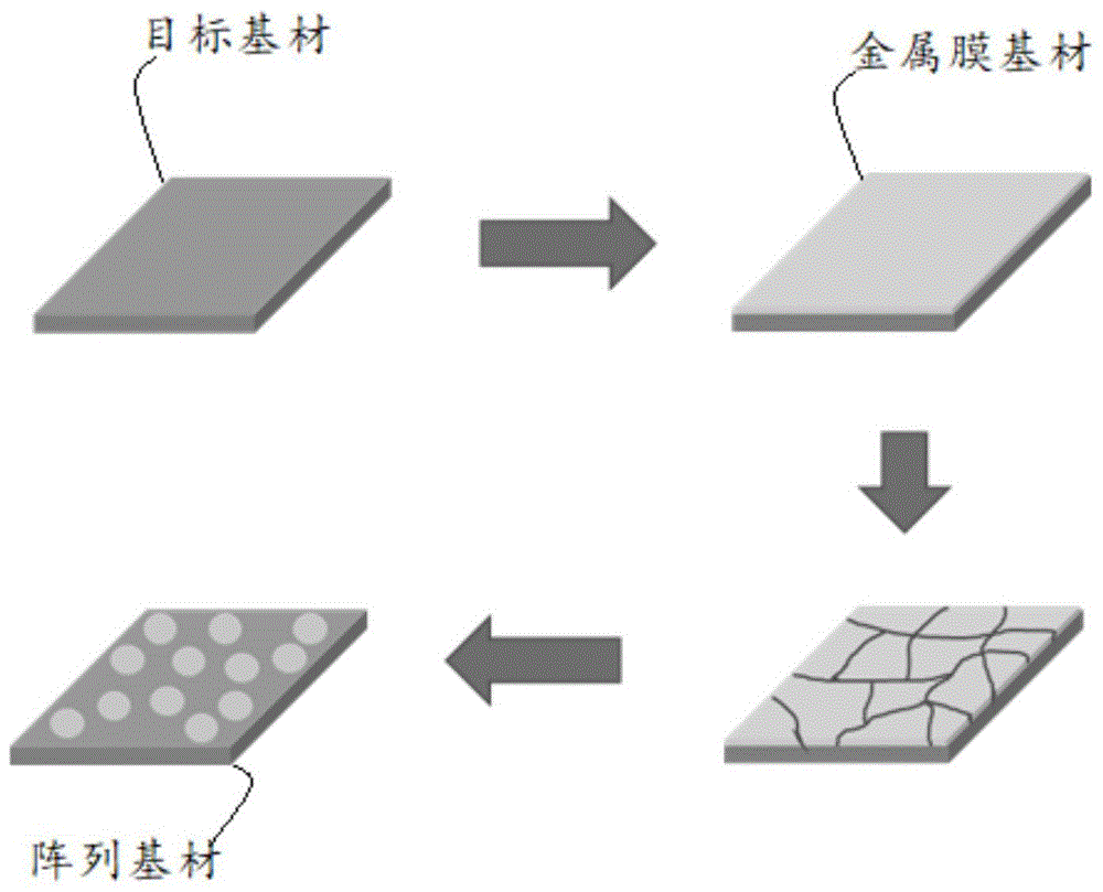
图1为本发明的纳米颗粒阵列基材的制备方法的一些实施例中目标基材沉积金属膜形成金属膜基材后,裂解为纳米颗粒阵列基材的一个示意图;Fig. 1 is a schematic diagram of the target substrate being cracked into a nanoparticle array substrate after depositing a metal film to form a metal film substrate in some embodiments of the method for preparing a nanoparticle array substrate of the present invention;
图2为本发明的纳米颗粒阵列基材的制备方法的一些实施例中金属膜在快速热退火处理后裂解为颗粒的示意图。FIG. 2 is a schematic diagram of the cracking of the metal film into particles after rapid thermal annealing in some embodiments of the preparation method of the nanoparticle array substrate of the present invention.
图3为本发明一些实施例中制备的生物测序芯片基底的一个示意图;Fig. 3 is a schematic diagram of the biological sequencing chip substrate prepared in some embodiments of the present invention;
图4为本发明的纳米颗粒阵列基材的制备方法的一些实施例中纳米颗粒的平均尺寸与金属膜的厚度之间的一个关系示意图;Fig. 4 is a schematic diagram of the relationship between the average size of nanoparticles and the thickness of the metal film in some embodiments of the preparation method of the nanoparticle array substrate of the present invention;
图5为本发明的纳米颗粒阵列基材的制备方法的一些实施例中纳米颗粒的分布密度与金属膜的厚度之间的一个关系示意图;5 is a schematic diagram of the relationship between the distribution density of nanoparticles and the thickness of the metal film in some embodiments of the preparation method of the nanoparticle array substrate of the present invention;
图6为本发明的生物测序芯片基底的制备方法的一些实施例中对金属纳米颗粒进行引物固定处理的一个示意图;Fig. 6 is a schematic diagram of the primer immobilization treatment of metal nanoparticles in some embodiments of the preparation method of the biological sequencing chip substrate of the present invention;
图7是纳米颗粒的阵列基材与硫醇化的寡核苷酸在引物固定处理前的一个示意图;7 is a schematic diagram of an array substrate of nanoparticles and thiolated oligonucleotides before primer immobilization treatment;
图8是纳米颗粒的阵列基材与硫醇化的寡核苷酸在引物固定处理后的一个示意图。Figure 8 is a schematic diagram of a nanoparticle array substrate with thiolated oligonucleotides after primer immobilization treatment.
具体实施方式Detailed ways
下面结合附图对本发明做进一步的详细说明,以令本领域技术人员参照说明书文字能够据以实施。The present invention will be further described in detail below in conjunction with the accompanying drawings, so that those skilled in the art can implement it with reference to the description.
本申请实施例中的术语“包括”和“设置有”以及它们任何变形,意图在于覆盖不排他的包含。例如包含了一系列步骤或单元的过程、方法、系统、产品或设备没有限定于已列出的步骤或单元,而是可选地还包括没有列出的步骤或单元,或可选地还包括对于这些过程、方法、产品或设备固有的其它步骤或单元。The terms "comprising" and "provided with" and any variations thereof in the embodiments of the present application are intended to cover non-exclusive inclusion. For example, a process, method, system, product or device comprising a series of steps or units is not limited to the listed steps or units, but optionally also includes unlisted steps or units, or optionally further includes For other steps or units inherent in these processes, methods, products or apparatuses.
除以上所述外,仍需要强调的是,在本文中提及“实施例”意味着,结合实施例描述的特定特征、结构或特性可以包含在本申请的至少一个实施例中。在说明书中的各个位置出现该短语并不一定均是指相同的实施例,也不是与其它实施例互斥的独立的或备选的实施例。本领域技术人员显式地和隐式地理解的是,本文所描述的实施例可以与其它实施例相结合。In addition to the above, it still needs to be emphasized that referring to "an embodiment" herein means that a specific feature, structure or characteristic described in connection with the embodiment may be included in at least one embodiment of the present application. The occurrences of this phrase in various places in the specification are not necessarily all referring to the same embodiment, nor are separate or alternative embodiments mutually exclusive of other embodiments. It is understood explicitly and implicitly by those skilled in the art that the embodiments described herein can be combined with other embodiments.
<第一方面:纳米颗粒阵列基材的制备方法><First Aspect: Preparation Method of Nanoparticle Array Substrate>
退火(Annealing)是将金属缓慢加热到一定温度,保持足够时间,然后以适宜速度冷却的一种金属热处理工艺。相应地,快速热退火(Rapid Thermal Annealing,简称RTA)一般指的是,对工件依次进行加热处理、退火处理和冷却处理;具体来说,要将工件从室温快速加热到目标温度,之后根据材料和工件尺寸采用对应的退火时间和退火温度,然后进行快速冷却至室温,目的是使金属内部组织达到或接近平衡状态,获得良好的工艺性能和使用性能。Annealing is a metal heat treatment process in which the metal is slowly heated to a certain temperature, kept for a sufficient time, and then cooled at an appropriate speed. Correspondingly, rapid thermal annealing (RTA for short) generally refers to sequentially heating, annealing and cooling the workpiece; specifically, rapidly heating the workpiece from room temperature to the target temperature, and then according to the material The annealing time and annealing temperature corresponding to the size of the workpiece are adopted, and then rapidly cooled to room temperature, the purpose is to make the internal structure of the metal reach or approach the equilibrium state, and obtain good process performance and use performance.
在加热处理阶段,加热速度可根据需要调节,加热温度随加热时间呈线性增加。加热处理也可以分阶段完成,即将加热时间划分成多个时间段,在每个时间段通过不同的温度改变斜率来实现加热处理。In the heating treatment stage, the heating speed can be adjusted according to the needs, and the heating temperature increases linearly with the heating time. The heat treatment can also be completed in stages, that is, the heating time is divided into multiple time periods, and the heat treatment is realized by changing the slope of the temperature in each time period.
在退火处理阶段,实际的退火方式是存在多种的,可以根据需要进行设定。例如,在退火时间内,退火温度可以被设置为一直保持不变,也可以被设置为随时间变化。In the annealing treatment stage, there are many kinds of actual annealing methods, which can be set according to needs. For example, during the annealing time, the annealing temperature can be set to remain constant all the time, or can be set to change with time.
通过上述的快速热退火处理,可以将目标基材上沉积的金属膜裂解为包含多个纳米颗粒的纳米颗粒阵列。Through the aforementioned rapid thermal annealing treatment, the metal film deposited on the target substrate can be cracked into a nanoparticle array comprising a plurality of nanoparticles.
根据以上构思,第一方面提供了一种纳米颗粒的阵列基材制备方法,包括:According to the above idea, the first aspect provides a method for preparing a nanoparticle array substrate, including:
在目标基材上沉积金属膜,形成金属膜基材;Deposit a metal film on the target substrate to form a metal film substrate;
快速热退火处理金属膜基材,使金属膜形成纳米颗粒阵列,得到阵列基材,该阵列基材用于制备生物测序芯片基底。The rapid thermal annealing treatment of the metal film base material makes the metal film form a nano particle array to obtain an array base material, and the array base material is used for preparing a biological sequencing chip base material.
需要说明的是,基材指的是用于制作芯片的基板材料。目标基材可以选自由硅晶、云母、玻璃或石英等材料制备的基材,即目标基材可以选自硅晶基材、玻璃基材、云母基材或石英基材中的一种。进一步地,所述硅晶基材为单晶硅圆基材。It should be noted that the base material refers to a substrate material used for making a chip. The target substrate can be selected from substrates prepared from materials such as silicon crystal, mica, glass or quartz, that is, the target substrate can be selected from one of silicon crystal substrates, glass substrates, mica substrates or quartz substrates. Further, the silicon crystal substrate is a single crystal silicon wafer substrate.
所述金属膜中的金属可以是金、铂、银、铜等,本领域技术人员可以根据需要进行选取。The metal in the metal film can be gold, platinum, silver, copper, etc., which can be selected by those skilled in the art according to needs.
在上述基础上,通过调节金属膜的厚度,快速热退火的加热速度、退火温度以及退火时间,可以调节或控制纳米颗粒的形状、尺寸大小、分布密度和间距,从而形成合适的纳米颗粒阵列。需要说明的是,这里的分布密度,亦称“概率的分布密度”,能够反映纳米颗粒阵列中相邻的纳米颗粒之间的间距。根据纳米颗粒的尺寸(纳米颗粒的尺寸可以通过粒径来表征)和分布密度就可以确定相邻纳米颗粒之间的间距。On the basis of the above, by adjusting the thickness of the metal film, the heating rate of rapid thermal annealing, annealing temperature and annealing time, the shape, size, distribution density and spacing of nanoparticles can be adjusted or controlled, so as to form a suitable nanoparticle array. It should be noted that the distribution density here, also known as "probability distribution density", can reflect the spacing between adjacent nanoparticles in the nanoparticle array. The spacing between adjacent nanoparticles can be determined according to the size of the nanoparticles (the size of the nanoparticles can be characterized by the particle diameter) and the distribution density.
由于沉积金属膜和快速热退火处理的过程是易于调节和控制的,所以,根据上述方法,能够提高调节纳米颗粒的形状、大小和分布密度的便利度,更有利于符合生产需求的金属纳米颗粒阵列的制备,例如高分布密度的、相邻纳米颗粒之间互相不接触的阵列基材。Since the process of depositing metal film and rapid thermal annealing treatment is easy to adjust and control, according to the above method, the convenience of adjusting the shape, size and distribution density of nanoparticles can be improved, which is more conducive to metal nanoparticles that meet production requirements. Preparation of arrays, such as array substrates with high distribution density and no contact between adjacent nanoparticles.
尽管,金属膜的厚度、加热速度、退火温度和退火时间,与纳米颗粒的形状、大小、分布密度和间距之间呈比较复杂的关系。但是仍然具备以下所述的明显特征。这些特征能够帮助本领域技术人员获取到理想的纳米颗粒阵列基材。Although, the thickness of the metal film, heating rate, annealing temperature and annealing time, and the shape, size, distribution density and spacing of nanoparticles are more complicated. However, it still has the distinctive features described below. These features can help those skilled in the art to obtain an ideal nanoparticle array substrate.
一般在快速热退火处理中,改变加热速度,可以控制纳米颗粒的大小。例如,迅速升至高温,可把金属膜分裂成多个小块,得到以小尺寸为主的纳米颗粒群;而降低升温速度,则有利于大尺寸纳米颗粒的形成。Generally, in rapid thermal annealing treatment, the size of nanoparticles can be controlled by changing the heating rate. For example, if the temperature is raised rapidly, the metal film can be split into multiple small pieces to obtain a group of mainly small-sized nanoparticles; while reducing the heating rate is conducive to the formation of large-sized nanoparticles.
得益于较大球体的较低表面能,较长的退火时间可使较大的纳米颗粒变大且成球形、而较小的纳米颗粒则变小以至于消失。而在另一方面,较短的退火时间则不能将纳米颗粒转变为理想的纳米球形,并且呈现为不规则的形状和大小。所以,在一定条件下,退火时间越长,纳米颗粒的尺寸越大。Benefiting from the lower surface energy of larger spheres, longer annealing times cause larger nanoparticles to grow and become spherical, while smaller nanoparticles shrink to disappear. On the other hand, shorter annealing times failed to transform the nanoparticles into ideal nanospheres and exhibited irregular shapes and sizes. Therefore, under certain conditions, the longer the annealing time, the larger the size of the nanoparticles.
与退火时间类似,在一定条件下,退火温度越高,纳米颗粒的尺寸越大。Similar to the annealing time, under certain conditions, the higher the annealing temperature, the larger the size of the nanoparticles.
而金属膜的厚度则可以用来控制金属膜中金属的总量,从而影响纳米颗粒的大小和间距。如果金属的总量一定,纳米颗粒的间距与尺寸则成反相关关系。当金的总量增加时,保持纳米颗粒的尺寸,纳米颗粒的间距会下降。The thickness of the metal film can be used to control the total amount of metal in the metal film, which affects the size and spacing of the nanoparticles. If the total amount of metal is constant, the spacing and size of nanoparticles are inversely correlated. As the total amount of gold increases, the nanoparticle spacing decreases while maintaining the size of the nanoparticles.
进一步地,将金膜的厚度、加热速度、退火时间和退火温度四个因素结合在一起后,就可以实现对纳米颗粒形状、大小和间距的更为准确地、进一步地综合控制。具体来说,金膜的厚度薄,加热速度快,退火时间越短,退火温度越低,可以得到间距小、分布密度大的小颗粒;金膜的厚度薄,加热速度快,退火时间越长,退火温度越高,可以得到间距大、低分布密度的大颗粒;金膜的厚度厚,加热速度快,退火温度高,退火时间越短,可以得到间距小、分布密度大的大颗粒;金膜的厚度越厚,加热速度快,退火温度高,退火时间越长,可以得到间距大、低分布密度的超大颗粒。Furthermore, after combining the four factors of gold film thickness, heating rate, annealing time and annealing temperature, more accurate and comprehensive control of the shape, size and spacing of nanoparticles can be realized. Specifically, the thickness of the gold film is thin, the heating rate is fast, the annealing time is shorter, and the annealing temperature is lower, and small particles with small spacing and large distribution density can be obtained; the thickness of the gold film is thin, the heating rate is fast, and the annealing time is longer , the higher the annealing temperature, the large particles with large spacing and low distribution density can be obtained; the thickness of gold film is thick, the heating speed is fast, the annealing temperature is high, and the annealing time is short, large particles with small spacing and large distribution density can be obtained; The thicker the film, the faster the heating speed, the higher the annealing temperature, and the longer the annealing time, the super-large particles with large spacing and low distribution density can be obtained.
此外,当所述快速退火处理的退火方式为变温退火时,即让退火温度缓缓降低或升高,也可以以实现对纳米颗粒形状的控制,得到想要的颗粒大小和表面浓度。例如,在快速热退火时,采用高速升温,可把金属膜分裂成多个小块,得到以小颗粒为主的颗粒群;而在变温退火时,使用逐渐降低的退火温度,则能防止大颗粒的形成,同时颗粒外形更圆润。In addition, when the annealing method of the rapid annealing treatment is variable temperature annealing, that is, the annealing temperature is slowly lowered or increased, and the shape of the nanoparticles can be controlled to obtain the desired particle size and surface concentration. For example, in rapid thermal annealing, the metal film can be split into multiple small pieces by using high-speed temperature rise, and a particle group mainly composed of small particles can be obtained; while in variable temperature annealing, the use of gradually decreasing annealing temperature can prevent large The formation of particles, while the particle shape is more rounded.
在一些实施方式中,可以根据沉积的时间调节所述金属膜的厚度。一般来说,沉积时间和金属膜的厚度呈正比关系。示例性地,可以通过热蒸发或电子束蒸发将厚度可调的金属膜沉积在目标基材干净的平坦表面上;在具体的生产实践中,一般会通过蒸镀仪进行沉积处理,而蒸镀仪上一般就会有厚度读数。In some embodiments, the thickness of the metal film can be adjusted according to the deposition time. In general, the deposition time is directly proportional to the thickness of the metal film. Exemplarily, the metal film with adjustable thickness can be deposited on the clean flat surface of the target substrate by thermal evaporation or electron beam evaporation; There will usually be a thickness reading on the gauge.
在一些实施方式中,所述金属膜的厚度在2到250nm之间。进一步地,所述金属膜的厚度在2到8nm之间。In some embodiments, the thickness of the metal film is between 2 and 250 nm. Further, the thickness of the metal film is between 2 and 8 nm.
在一些实施方式中,所述快速热退火处理的退火温度在200到1100度之间,所述快速热退火处理的退火时间在30到300秒之间。In some embodiments, the annealing temperature of the rapid thermal annealing treatment is between 200 and 1100 degrees, and the annealing time of the rapid thermal annealing treatment is between 30 and 300 seconds.
示例性地,所述金属膜的厚度为4nm,所述快速热退火处理的退火温度为450度,退火时间为180秒。在这种条件下,4nm厚的金属膜在经过经热退火处理后,能够形成平均尺寸为30nm的均匀的、球形的纳米颗粒阵列。换言之,纳米颗粒的平均粒径为30nm,分布密度为103个/μm2(或10x1010个/cm2)。Exemplarily, the thickness of the metal film is 4 nm, the annealing temperature of the rapid thermal annealing treatment is 450 degrees, and the annealing time is 180 seconds. Under these conditions, a 4nm thick metal film can form a uniform, spherical nanoparticle array with an average size of 30nm after thermal annealing. In other words, the average particle size of the nanoparticles is 30 nm, and the distribution density is 10 3 /μm 2 (or 10×10 10 /cm 2 ).
进一步地,所述在目标基材上沉积金属膜,形成金属膜基材的步骤,包括:Further, the step of depositing a metal film on the target substrate to form a metal film substrate includes:
清洁目标基材的表面;得到第一洁净基材;cleaning the surface of the target substrate; obtaining the first clean substrate;
对第一洁净基材镀金处理,形成金属膜基材。Gold plating is performed on the first clean base material to form a metal film base material.
进一步地,所述清洁目标基材的表面的步骤包括:Further, the step of cleaning the surface of the target substrate comprises:
用第一清洗剂和第二清洗剂交替清洗目标基材;其中,第一清洗剂为乙醇或异丙醇,第二清洗剂为水。The target substrate is alternately cleaned with the first cleaning agent and the second cleaning agent; wherein, the first cleaning agent is ethanol or isopropanol, and the second cleaning agent is water.
进一步地,所述对第一洁净基材镀金处理,形成金属膜基材的步骤,包括:Further, the step of gold-plating the first clean substrate to form a metal film substrate includes:
用清洗液清洗第一洁净基材,得到所述第二洁净基材,其中,所述清洗液为食人鱼溶液(Piranha溶液);Washing the first clean substrate with a cleaning solution to obtain the second clean substrate, wherein the cleaning solution is a piranha solution (Piranha solution);
对所述第二洁净基材镀金处理,形成所述金属膜基材。Gold plating is performed on the second clean substrate to form the metal film substrate.
在本发明实施例中,用乙醇或异丙醇、水交替清洗直径为预定尺寸(例如4-8英寸)的目标基材表面,得到第一洁净基材后,再使用Pi ranha溶液清洗第一洁净基材,能使获取的第二洁净基材更好地附着金属膜。In the embodiment of the present invention, the surface of the target substrate whose diameter is a predetermined size (for example, 4-8 inches) is alternately cleaned with ethanol or isopropanol and water, and after the first clean substrate is obtained, the first clean substrate is cleaned with Pi ranha solution. The clean substrate can make the obtained second clean substrate adhere to the metal film better.
进一步地,对所述第二洁净基材镀金处理包括:Further, the gold plating treatment on the second clean substrate includes:
在电阻式蒸发器炉或者电子束蒸发器中对第二洁净基材进行镀金处理。A second clean substrate is gold plated in either a resistive evaporator furnace or an electron beam evaporator.
<第二方面:纳米颗粒的阵列基材><Second Aspect: Nanoparticle Array Substrate>
第二方面提供了一种纳米颗粒的阵列基材,根据第一方面所述纳米颗粒的阵列基材制备方法制备而成。The second aspect provides a nanoparticle array substrate prepared according to the preparation method of the nanoparticle array substrate described in the first aspect.
<第三方面:生物测序芯片基底的制备方法><Third Aspect: Preparation Method of Biological Sequencing Chip Substrate>
第三方面提供了一种生物测序芯片基底的制备方法The third aspect provides a method for preparing a biological sequencing chip substrate
对第一方面或第二方面中的阵列基材进行引物固定处理,得到芯片基底。Immobilizing primers on the array substrate in the first aspect or the second aspect to obtain a chip substrate.
第三方面提供的生物测序芯片基底中只有金属纳米颗粒是活性的,能够与引物反应;芯片基底的其他地方会很干净,因此可以降低测量时产生的噪音。In the biological sequencing chip substrate provided by the third aspect, only the metal nanoparticles are active and can react with the primers; other parts of the chip substrate will be very clean, so noise generated during measurement can be reduced.
在一些实施方式中,所述引物固定处理包括:In some embodiments, the primer immobilization treatment comprises:
应用硫醇化的寡核苷酸修饰所述阵列基材的纳米颗粒;或者modifying the nanoparticles of the array substrate with thiolated oligonucleotides; or
在所述阵列基材的纳米颗粒的表面生成活性基团后,应用修饰的寡核苷酸进行修饰处理。After the active groups are generated on the surface of the nanoparticles of the array substrate, the modified oligonucleotides are used for modification treatment.
关于修饰的寡核苷酸的具体选择,可以根据纳米颗粒的表面性质进行确定。例如当纳米颗粒的表面带有醛基的连接物时,修饰的寡核苷酸可以带有氨基,从而和醛基反应生成共价连接;又比如当纳米颗粒的表面接的是带有抗生物素蛋白的连接物时,寡核苷酸可以带有链霉亲和素,从而可以和抗生物素蛋白形成稳定的连接。Regarding the specific choice of modified oligonucleotides, it can be determined according to the surface properties of the nanoparticles. For example, when the surface of the nanoparticle has an aldehyde-based linker, the modified oligonucleotide can have an amino group to react with the aldehyde group to form a covalent link; When using the linker of avidin, the oligonucleotide can have streptavidin, so that it can form a stable connection with avidin.
在一些实施方式中,所述活性基团选自羟基、羧基、氨基、环氧基、醛基、N羟基琥珀酰亚胺基、活化氨基、巯基、叠氮基。In some embodiments, the reactive group is selected from hydroxyl, carboxyl, amino, epoxy, aldehyde, N-hydroxysuccinimide, activated amino, mercapto, and azido.
在一些实施方式中,当所述活性基团为羟基时,所述活性剂为羟基硫醇;当所述活性基团为羧基时,所述活性剂为羧基硫醇。In some embodiments, when the active group is a hydroxyl group, the active agent is a hydroxyl thiol; when the active group is a carboxyl group, the active agent is a carboxyl thiol.
<第四方面:生物测序芯片基底><Fourth Aspect: Biological Sequencing Chip Substrate>
第四方面提供了一种生物测序芯片基底,根据第三方面所述生物测序芯片基底制备方法制备而成。The fourth aspect provides a biological sequencing chip substrate prepared according to the method for preparing the biological sequencing chip substrate described in the third aspect.
<第五方面:生物测序芯片><Fifth Aspect: Biological Sequencing Chip>
第四方面提供了一种生物测序芯片,包含第四方面所述的生物测序芯片基底。The fourth aspect provides a biological sequencing chip, including the biological sequencing chip substrate described in the fourth aspect.
本申请实施例提供的生物测序芯片基底上引物的表面修饰浓度均一,能够使得由PCR反应次数控制的簇大小均一,可以提高荧光显微镜下有效光点(簇)的数量,从而大幅提升通量。基于本申请实施例提供的生物测序芯片基底开发的生物测序芯片具有高重复性和高分布密度。The surface modification concentration of the primers on the biological sequencing chip substrate provided by the embodiment of the present application is uniform, which can make the cluster size controlled by the number of PCR reactions uniform, and can increase the number of effective light spots (clusters) under the fluorescence microscope, thereby greatly increasing the throughput. The biological sequencing chip developed based on the biological sequencing chip substrate provided in the embodiment of the present application has high repeatability and high distribution density.
生物测序芯片基底制备实验:Biological sequencing chip substrate preparation experiment:
(1)选取单晶硅圆基材作为目标基材。(1) Select the single crystal silicon wafer substrate as the target substrate.
(2)用乙醇或异丙醇作为第一清洗剂、水作作为第二清洗剂,交替清洗直径为4英寸的目标基材表面,得到第一洁净基材;然后使用Piranha溶液清洁第一洁净基材,得到第二洁净基材。(2) Use ethanol or isopropanol as the first cleaning agent and water as the second cleaning agent to alternately clean the surface of the target substrate with a diameter of 4 inches to obtain the first clean substrate; then use Piranha solution to clean the first clean substrate to obtain a second clean substrate.
(3)将第二洁净基材置于Edward 306A resistive evaporator炉中,镀上2-8纳米厚的金层,形成金属膜,得到金属膜基材。(3) The second clean substrate is placed in an Edward 306A resistive evaporator furnace, and a gold layer with a thickness of 2-8 nanometers is plated to form a metal film to obtain a metal film substrate.
(4)将金属膜基材加热至450基材的温度下退火3min,得到纳米颗粒的阵列基材。(4) Heating the metal film substrate to a temperature of 450° C. for 3 minutes and annealing to obtain a nanoparticle array substrate.
(5)将阵列基材切割后,清洗吹干,置于浓度为1.0mol/L的巯基修饰的PolyT核酸引物的K2HPO4溶液中(K2HPO4溶液的浓度为150mmol/L),反应1小时,以进行引物固定处理;然后依次用3XSSC溶液(含质量分数为0.1%的Triton)、0.2mol/L K2HPO4溶液、150mmol/LHEPES与150mmol/L NaCl的混合溶液及超纯水清洗后,含有PolyT引物的生物测序芯片基底制作完成。(5) After cutting the array substrate, wash and dry it, and place it in a
实验结果:Experimental results:
图1展示了目标基材沉积金属膜形成金属膜基材后,裂解为纳米颗粒阵列基材的示意图。Figure 1 shows a schematic diagram of the target substrate being cracked into a nanoparticle array substrate after depositing a metal film to form a metal film substrate.
图2进一步展示了4纳米厚度的金属膜在快速热退火处理后的示意图。FIG. 2 further shows a schematic diagram of a metal film with a thickness of 4 nm after rapid thermal annealing.
结合图1-2所示,可以看出,4nm厚的金属膜在经过快速热退火处理后转变为均匀的、球形的且相邻颗粒之间不接触的金属纳米颗粒阵列。其中,金属纳米颗粒平均粒径为30nm,分布密度为103/μm2。As shown in Figures 1-2, it can be seen that the 4nm thick metal film is transformed into a uniform, spherical metal nanoparticle array without contact between adjacent particles after rapid thermal annealing treatment. Among them, the average particle diameter of metal nanoparticles is 30nm, and the distribution density is 10 3 /μm 2 .
图3展示了制备的晶圆级尺寸的生物测序芯片基底。Fig. 3 shows the prepared wafer-scale biological sequencing chip substrate.
图4-5显示了450℃的退火温度条件下,退火处理3分钟,纳米颗粒的平均大小(平均大小即平均尺寸)和分布密度对金属膜厚度的依赖性。结果表明,将金属膜的膜厚度从2nm增加到8nm可以降低球形的金属纳米颗粒的分布密度,但会增加球形的金属纳米颗粒的平均尺寸。因此,形成均匀的金纳米颗粒阵列,不仅需要合适的金属膜厚度,还需要相应的退火工艺。Figures 4-5 show the dependence of the average size (average size is the average size) and distribution density of nanoparticles on the thickness of the metal film under the annealing temperature condition of 450° C. and annealing treatment for 3 minutes. The results show that increasing the film thickness of the metal film from 2nm to 8nm can reduce the distribution density of spherical metal nanoparticles, but increase the average size of spherical metal nanoparticles. Therefore, forming a uniform gold nanoparticle array requires not only an appropriate metal film thickness, but also a corresponding annealing process.
在金属纳米颗粒形成之后,可以使用硫醇化学方法,通过硫醇化的寡核苷酸直接地对金属纳米颗粒进行引物固定处理,完成引物修饰,以用于形成生物测序芯片基底,具体如图6-8所示;其中,图6完整的反映了引物固定处理的过程,图7反映的是引物固定处理前的纳米颗粒的阵列基材与硫醇化的寡核苷酸,图8反映的是在图7的基础上对纳米颗粒的阵列基材进行引物固定处理后的结果。结合图6-8可以发现,经过引物固定处理后,硫醇化的寡核苷酸20与纳米颗粒的阵列基材10上的金属纳米颗粒11结合在了一起。After the metal nanoparticles are formed, the thiol chemical method can be used to directly immobilize the metal nanoparticles with primers through thiol oligonucleotides to complete the primer modification for the formation of the biological sequencing chip substrate, as shown in Figure 6. -8; wherein, Fig. 6 completely reflects the process of primer immobilization treatment, Fig. 7 reflects the array base material and thiolated oligonucleotides of nanoparticles before primer immobilization treatment, and Fig. 8 reflects the process in Figure 7 is based on the results of the primer immobilization treatment on the nanoparticle array substrate. 6-8, it can be found that after the primer immobilization treatment, the
除了以上方法外,还可以通过与修饰的寡核苷酸具有反应性的其他表面官能团间接地对金属纳米颗粒进行引物修饰,以形成生物测序芯片基底。In addition to the above methods, metal nanoparticles can also be indirectly modified with primers through other surface functional groups reactive with the modified oligonucleotides to form a biological sequencing chip substrate.
用引物修饰金属纳米颗粒后,底物即可用于桥连(bridge)或模板步移(templatewalking)扩增。由于引物区域是不连续的,并且受到金属纳米颗粒边界的限制,因此簇的大小在过度扩增时只受到金属纳米颗粒大小的限制,而不会过度生长成大的簇。这样得到的簇大小均一,不会受到表面反应活性不均一性的影响。After modifying the metal nanoparticles with primers, the substrate is ready for bridge or template walking amplification. Since the primer region is discontinuous and limited by the metal nanoparticle boundaries, the cluster size is only limited by the metal nanoparticle size when over-amplified without overgrowing into large clusters. The resulting clusters are uniform in size and are not affected by inhomogeneity in surface reactivity.
尽管本发明的实施方案已公开如上,但其并不仅仅限于说明书和实施方式中所列运用,它完全可以被适用于各种适合本发明的领域,对于熟悉本领域的人员而言,可容易地实现另外的修改,因此在不背离权利要求及等同范围所限定的一般概念下,本发明并不限于特定的细节和这里示出与描述的图例。Although the embodiment of the present invention has been disclosed as above, it is not limited to the use listed in the specification and implementation, it can be applied to various fields suitable for the present invention, and it can be easily understood by those skilled in the art Therefore, the invention is not limited to the specific details and examples shown and described herein without departing from the general concept defined by the claims and their equivalents.
Claims (7)
Priority Applications (1)
| Application Number | Priority Date | Filing Date | Title |
|---|---|---|---|
| CN202110858734.3A CN113846292B (en) | 2021-07-28 | 2021-07-28 | Biological sequencing chip, substrate, nanoparticle array substrate and preparation method |
Applications Claiming Priority (1)
| Application Number | Priority Date | Filing Date | Title |
|---|---|---|---|
| CN202110858734.3A CN113846292B (en) | 2021-07-28 | 2021-07-28 | Biological sequencing chip, substrate, nanoparticle array substrate and preparation method |
Publications (2)
| Publication Number | Publication Date |
|---|---|
| CN113846292A CN113846292A (en) | 2021-12-28 |
| CN113846292B true CN113846292B (en) | 2023-05-23 |
Family
ID=78975214
Family Applications (1)
| Application Number | Title | Priority Date | Filing Date |
|---|---|---|---|
| CN202110858734.3A Active CN113846292B (en) | 2021-07-28 | 2021-07-28 | Biological sequencing chip, substrate, nanoparticle array substrate and preparation method |
Country Status (1)
| Country | Link |
|---|---|
| CN (1) | CN113846292B (en) |
Families Citing this family (1)
| Publication number | Priority date | Publication date | Assignee | Title |
|---|---|---|---|---|
| CN115356299B (en) * | 2022-04-13 | 2025-12-02 | 中国科学院上海微系统与信息技术研究所 | A biochemical detection chip and its preparation method |
Family Cites Families (4)
| Publication number | Priority date | Publication date | Assignee | Title |
|---|---|---|---|---|
| DE60305323T2 (en) * | 2002-07-05 | 2006-12-28 | Koninklijke Philips Electronics N.V. | METHOD FOR MANUFACTURING A STREADER |
| CN101172573A (en) * | 2006-11-01 | 2008-05-07 | 国家纳米技术与工程研究院 | Silver nano-grain array mould plate and preparation method thereof |
| CN102806354A (en) * | 2012-07-31 | 2012-12-05 | 东南大学 | Method for preparing gold nanoparticles by annealing of gold film |
| CN112038442B (en) * | 2020-09-10 | 2022-02-15 | 华南师范大学 | A kind of photoelectric detector and preparation method thereof |
-
2021
- 2021-07-28 CN CN202110858734.3A patent/CN113846292B/en active Active
Also Published As
| Publication number | Publication date |
|---|---|
| CN113846292A (en) | 2021-12-28 |
Similar Documents
| Publication | Publication Date | Title |
|---|---|---|
| Bayrak et al. | DNA-mold templated assembly of conductive gold nanowires | |
| US20220098653A1 (en) | Structured substrates for improving detection of light emissions and methods relating to the same | |
| Peterson et al. | Kinetic control of hybridization in surface immobilized DNA monolayer films | |
| KR100682919B1 (en) | Formation method of fine metal thin film pattern, biomaterial fixing substrate and biochip | |
| JP4466074B2 (en) | Fine metal structure and manufacturing method thereof, and fine mold and device | |
| Aqua et al. | Controlling the adsorption and reactivity of DNA on gold | |
| US20060057604A1 (en) | Method for electrically detecting oligo-nucleotides with nano-particles | |
| CN102414557A (en) | Electrical sensor for ultrasensitive nucleic acid detection | |
| CN103938158A (en) | SERS (Surface Enhanced Raman Scattering) substrate with self-assembled spherical array and preparation method thereof | |
| WO2010088726A1 (en) | Fabrication of nanoparticles on solid surfaces | |
| JP2010151848A (en) | Method for immobilizing self-organizing material or fine particle on substrate, and substrate manufactured by using such method | |
| CN113846292B (en) | Biological sequencing chip, substrate, nanoparticle array substrate and preparation method | |
| CN102482717B (en) | Carrier for holding nucleic acids | |
| Yi et al. | Patterned growth of vertically aligned silicon nanowire arrays for label-free DNA detection using surface-enhanced Raman spectroscopy | |
| Domínguez et al. | Hydration induced stress on DNA monolayers grafted on microcantilevers | |
| JP3398366B2 (en) | Method for producing microarray for DNA analysis | |
| WO2008028011A2 (en) | Compositions and methods for preserving permeation layers for use on active electronic matrix devices | |
| CN106048537A (en) | Method for preparing SERS substrate by combining colloidal sphere self-assembly with ion-sputtering coating | |
| JP4053288B2 (en) | Solid support for immobilizing oligonucleotides | |
| US9110056B2 (en) | Surface treatment | |
| CN108417475A (en) | A kind of preparation method of the metal Nano structure array based on interface induced growth | |
| EP1250584B1 (en) | Method for characterization and quality control of porous media | |
| Zhang et al. | A thermo-responsive rewritable plasmonic bio-memory by regulating single core-satellite gold nanocluster dissociation | |
| JPH06256753A (en) | Method for manufacturing orientation control thin film and orientation control thin film | |
| HK40041758B (en) | Dna-based digital information storage |
Legal Events
| Date | Code | Title | Description |
|---|---|---|---|
| PB01 | Publication | ||
| PB01 | Publication | ||
| SE01 | Entry into force of request for substantive examination | ||
| SE01 | Entry into force of request for substantive examination | ||
| GR01 | Patent grant | ||
| GR01 | Patent grant |