Disclosure of Invention
An object of the present invention is to solve at least the above problems and to provide at least the advantages described later.
An object of the present invention is to solve at least the following problems: (1) how to adjust the size and distribution density of the nano particles fixed on the plane, so that the distance between the adjacent nano particles can be adjusted and the adjacent nano particles are not contacted with each other; (2) how to provide a second-generation biological sequencing chip with high repeatability and high density, and a base material and a substrate thereof; (3) how to provide a clean biological sequencing chip substrate to reduce the noise of the biological sequencing chip during measurement.
Specifically, the invention is realized by the following technical scheme:
first aspect of the invention
In a first aspect, there is provided a method for preparing an array substrate of nanoparticles, comprising:
depositing a metal film on a target substrate to form a metal film substrate;
and carrying out rapid thermal annealing treatment on the metal film substrate to enable the metal film on the metal film substrate to form a nanoparticle array to obtain the nanoparticle array substrate, wherein the array substrate is used for preparing the biological sequencing chip substrate.
Since the processes of depositing the metal film and the rapid thermal annealing process are easily adjusted and controlled, according to the above method, it is possible to improve the convenience of adjusting the shape, size and distribution density of the nanoparticles, and to facilitate the preparation of a metal nanoparticle array that meets the production requirements, such as an array substrate having a high distribution density in which adjacent nanoparticles are not in contact with each other.
Nanoparticles, when immobilized to the plane of the array substrate, can act as carriers for desirable clusters due to their uniform size and surface chemistry. Therefore, according to the method for preparing an array substrate of nanoparticles provided by the first aspect, a uniform, wafer-sized, clean-background array substrate can be manufactured on a large scale, and used as a carrier for clusters; therefore, the method can be used for manufacturing a second-generation biological sequencing chip with high repeatability and high density.
Second aspect of the invention
A second aspect provides a nanoparticle array substrate prepared according to the method for preparing a nanoparticle array substrate of the first aspect.
Third aspect of the invention
A third aspect provides a method for preparing a biological sequencing chip substrate, comprising:
and (3) carrying out primer fixing treatment on the array substrate in the second aspect to obtain the chip substrate.
Fourth aspect of the invention
The fourth aspect provides a biological sequencing chip substrate, which is prepared according to the preparation method of the biological sequencing chip substrate of the third aspect.
Fifth aspect of the invention
In a fifth aspect, there is provided a biological sequencing chip comprising the biological sequencing chip substrate of the fourth aspect.
Compared with the prior art, the technical effects of the embodiment of the invention at least comprise the following steps:
1. since the processes of depositing the metal film and the rapid thermal annealing treatment are easy to adjust and control, the method for preparing the nanoparticle array substrate according to the embodiment of the invention can improve the convenience of adjusting the shape, size and distribution density of the nanoparticles, and is more beneficial to the preparation of the metal nanoparticle array meeting the production requirement, such as an array substrate with high distribution density and without contact between adjacent nanoparticles.
2. The array substrate of nanoparticles provided by the embodiment of the application has a wafer-level size, and a biological sequencing chip is easy to manufacture. In addition, the size and spacing of the nanoparticles on the array substrate can be easily adjusted and precisely controlled, thus allowing for uniform, easily patterned fabrication.
3. On the biological sequencing chip substrate provided by the embodiment of the application, only the metal nanoparticles are active and can react with the primers, and the rest part of the substrate is very clean. Therefore, the biological sequencing chip prepared according to the aforementioned biological sequencing chip substrate can reduce noise generated at the time of measurement.
4. The surface modification concentration of the primers on the substrate of the biological sequencing chip provided by the embodiment of the application is uniform, the size of the clusters controlled by the PCR reaction times is uniform, the number of effective light spots (clusters) under a fluorescence microscope can be increased, and the flux is greatly improved.
5. The biological sequencing chip developed based on the biological sequencing chip substrate provided by the embodiment of the application has high repeatability and high distribution density.
Additional advantages, objects, and features of the invention will be set forth in part in the description which follows and in part will become apparent to those having ordinary skill in the art upon examination of the following or may be learned from practice of the invention.
Detailed Description
The present invention is further described in detail below with reference to the attached drawings so that those skilled in the art can implement the invention by referring to the description text.
The terms "including" and "provided" in the embodiments of the present application, as well as any variations thereof, are intended to cover non-exclusive inclusions. For example, a process, method, system, article, or apparatus that comprises a list of steps or elements is not limited to only those steps or elements listed, but may alternatively include other steps or elements not listed, or inherent to such process, method, article, or apparatus.
In addition to the foregoing, it should be emphasized that reference herein to "an embodiment" means that a particular feature, structure, or characteristic described in connection with the embodiment can be included in at least one embodiment of the application. The appearances of the phrase in various places in the specification are not necessarily all referring to the same embodiment, nor are separate or alternative embodiments mutually exclusive of other embodiments. It is explicitly and implicitly understood by one skilled in the art that the embodiments described herein can be combined with other embodiments.
< first aspect: preparation method of nanoparticle array substrate >
Annealing (Annealing) is a heat treatment process of metals in which the metal is slowly heated to a temperature, held for a sufficient time, and then cooled at a suitable rate. Correspondingly, Rapid Thermal Annealing (RTA) generally refers to heating, Annealing, and cooling a workpiece in sequence; specifically, the workpiece is rapidly heated from room temperature to a target temperature, then corresponding annealing time and annealing temperature are adopted according to the material and the size of the workpiece, and then rapid cooling is carried out to the room temperature, so that the internal structure of the metal reaches or approaches a balanced state, and good technological performance and service performance are obtained.
In the heating treatment stage, the heating speed can be adjusted according to needs, and the heating temperature is linearly increased along with the heating time. The heat treatment may also be done in stages, i.e. the heating time is divided into a plurality of time periods, the heat treatment being effected by different temperature change slopes in each time period.
In the annealing treatment stage, there are various actual annealing methods, and they may be set as necessary. For example, the annealing temperature may be set to be constant at all times during the annealing time, or may be set to vary with time.
Through the rapid thermal annealing process described above, the metal film deposited on the target substrate can be decomposed into a nanoparticle array including a plurality of nanoparticles.
According to the above concept, there is provided a method of preparing an array substrate of nanoparticles, including:
depositing a metal film on a target substrate to form a metal film substrate;
and (3) carrying out rapid thermal annealing treatment on the metal film substrate to enable the metal film to form a nanoparticle array to obtain an array substrate, wherein the array substrate is used for preparing a biological sequencing chip substrate.
The base material refers to a substrate material used for manufacturing a chip. The target substrate may be selected from substrates made of silicon, mica, glass or quartz, i.e. the target substrate may be selected from one of silicon substrates, glass substrates, mica substrates or quartz substrates. Further, the silicon crystal substrate is a single crystal silicon wafer substrate.
The metal in the metal film can be gold, platinum, silver, copper, etc., and can be selected by those skilled in the art according to the needs.
On the basis, the shape, the size, the distribution density and the spacing of the nano particles can be adjusted or controlled by adjusting the thickness of the metal film, the heating speed of the rapid thermal annealing, the annealing temperature and the annealing time, so that a proper nano particle array is formed. It should be noted that the distribution density, also referred to as "probability distribution density", can reflect the spacing between adjacent nanoparticles in the nanoparticle array. The spacing between adjacent nanoparticles can be determined based on the size of the nanoparticles (which can be characterized by the particle size) and the distribution density.
Since the processes of depositing the metal film and the rapid thermal annealing process are easily adjusted and controlled, according to the above method, it is possible to improve the convenience of adjusting the shape, size and distribution density of the nanoparticles, and to facilitate the preparation of a metal nanoparticle array that meets the production requirements, such as an array substrate having a high distribution density in which adjacent nanoparticles are not in contact with each other.
Although the thickness of the metal film, the heating rate, the annealing temperature, and the annealing time are in a relatively complicated relationship with the shape, size, distribution density, and spacing of the nanoparticles. But still possess the distinct features described below. These features can help one skilled in the art to obtain the desired nanoparticle array substrate.
Generally, in the rapid thermal annealing treatment, the size of the nanoparticles can be controlled by changing the heating speed. For example, rapid heating to high temperatures can break the metal film into multiple small pieces, resulting in a population of predominantly small-sized nanoparticles; and the temperature rise speed is reduced, so that the formation of large-size nano particles is facilitated.
Due to the lower surface energy of the larger spheres, longer annealing times can make the larger nanoparticles larger and spherical, while the smaller nanoparticles become smaller and disappear. On the other hand, a shorter annealing time does not transform the nanoparticles into the ideal nanospheres and assumes irregular shapes and sizes. Therefore, under certain conditions, the longer the annealing time, the larger the size of the nanoparticles.
Similar to the annealing time, under certain conditions, the higher the annealing temperature, the larger the size of the nanoparticles.
The thickness of the metal film can be used to control the total amount of metal in the metal film, thereby affecting the size and spacing of the nanoparticles. If the total amount of metal is constant, the spacing of the nanoparticles is inversely related to the size. As the total amount of gold increases, the nanoparticle size is maintained and the spacing between nanoparticles decreases.
Furthermore, after the four factors of the thickness, the heating speed, the annealing time and the annealing temperature of the gold film are combined together, the shape, the size and the distance of the nano particles can be more accurately and comprehensively controlled. Specifically, the gold film has thin thickness and high heating speed, the shorter the annealing time is, the lower the annealing temperature is, and small particles with small spacing and large distribution density can be obtained; the gold film has thin thickness and high heating speed, the longer the annealing time is, the higher the annealing temperature is, and large particles with large spacing and low distribution density can be obtained; the gold film has thick thickness, high heating speed and high annealing temperature, and the shorter the annealing time is, the larger the particles with small space and large distribution density can be obtained; the thicker the gold film is, the faster the heating speed, the higher the annealing temperature and the longer the annealing time are, the ultra-large particles with large spacing and low distribution density can be obtained.
In addition, when the annealing method of the rapid annealing treatment is temperature-variable annealing, that is, the annealing temperature is gradually decreased or increased, the shape of the nanoparticles can be controlled to obtain a desired particle size and surface concentration. For example, in rapid thermal annealing, a metal film can be divided into a plurality of small pieces by high-speed temperature rise to obtain a particle group mainly composed of small particles; and when the annealing temperature is changed, the gradually reduced annealing temperature is used, so that large particles can be prevented from being formed, and the appearance of the particles is more round.
In some embodiments, the thickness of the metal film may be adjusted according to the time of deposition. Generally, the deposition time is proportional to the thickness of the metal film. Illustratively, the thickness-tunable metal film may be deposited on a clean flat surface of a target substrate by thermal evaporation or electron beam evaporation; in particular production practices, the deposition process is typically conducted by an evaporator, which typically has a thickness reading.
In some embodiments, the metal film has a thickness between 2 and 250 nm. Further, the thickness of the metal film is between 2 and 8 nm.
In some embodiments, the rapid thermal anneal process has an anneal temperature between 200 and 1100 degrees and an anneal time between 30 and 300 seconds.
Illustratively, the metal film has a thickness of 4nm, the rapid thermal annealing treatment has an annealing temperature of 450 degrees and an annealing time of 180 seconds. Under these conditions, a 4nm thick metal film, after thermal annealing, was able to form a uniform, spherical nanoparticle array with an average size of 30 nm. In other words, the nanoparticles had an average particle diameter of 30nm and a distribution density of 103Per mu m2(or 10x1010Per cm2)。
Further, the step of depositing a metal film on a target substrate to form a metal film substrate includes:
cleaning a surface of a target substrate; obtaining a first clean substrate;
and carrying out gold plating treatment on the first clean substrate to form a metal film substrate.
Further, the step of cleaning the surface of the target substrate comprises:
alternately cleaning the target substrate with a first cleaning agent and a second cleaning agent; wherein the first cleaning agent is ethanol or isopropanol, and the second cleaning agent is water.
Further, the step of forming a metal film substrate by performing gold plating on the first clean substrate includes:
cleaning the first clean base material by using a cleaning solution to obtain a second clean base material, wherein the cleaning solution is a Piranha solution;
and carrying out gold plating treatment on the second clean substrate to form the metal film substrate.
In the embodiment of the present invention, after the surface of the target substrate having a predetermined diameter (e.g., 4 to 8 inches) is alternately cleaned with ethanol or isopropanol and water to obtain the first clean substrate, the first clean substrate is cleaned with the Pi ranha solution, so that the obtained second clean substrate can be better attached with the metal film.
Further, the gold plating process on the second clean substrate comprises:
the second clean substrate is gold plated in a resistance evaporator furnace or an electron beam evaporator.
< second aspect: nanoparticle array substrate >
In a second aspect, there is provided a nanoparticle array substrate prepared according to the method of the first aspect.
< third aspect: preparation method of biological sequencing chip substrate >
The third aspect provides a method for preparing a biological sequencing chip substrate
And (3) carrying out primer fixing treatment on the array substrate in the first aspect or the second aspect to obtain the chip substrate.
In the biological sequencing chip substrate provided by the third aspect, only the metal nanoparticles are active and can react with the primers; the chip substrate is cleaned elsewhere, so that noise generated during measurement can be reduced.
In some embodiments, the primer immobilization treatment comprises:
modifying the nanoparticles of the array substrate with thiolated oligonucleotides; or
After the active groups are generated on the surface of the nano-particles of the array substrate, modified oligonucleotides are applied for modification treatment.
The specific choice of modified oligonucleotide can be determined based on the surface properties of the nanoparticle. For example, when the surface of the nanoparticle has a linker with an aldehyde group, the modified oligonucleotide may have an amino group to react with the aldehyde group to form a covalent linkage; for another example, when the surface of the nanoparticle is attached with an avidin-containing linker, the oligonucleotide may be streptavidin-containing, thereby forming a stable linkage with avidin.
In some embodiments, the reactive group is selected from the group consisting of a hydroxyl group, a carboxyl group, an amino group, an epoxy group, an aldehyde group, an N-hydroxysuccinimide group, an activated amino group, a thiol group, and an azide group.
In some embodiments, when the reactive group is a hydroxyl group, the active agent is a hydroxythiol; when the reactive group is a carboxyl group, the active agent is a carboxythiol.
< fourth aspect: biological sequencing chip substrate >
The fourth aspect provides a biological sequencing chip substrate prepared by the preparation method of the biological sequencing chip substrate according to the third aspect.
< fifth aspect: biological sequencing chip >
A fourth aspect provides a biological sequencing chip comprising the biological sequencing chip substrate of the fourth aspect.
The surface modification concentration of the primers on the substrate of the biological sequencing chip provided by the embodiment of the application is uniform, the size of the clusters controlled by the PCR reaction times is uniform, the number of effective light spots (clusters) under a fluorescence microscope can be increased, and the flux is greatly improved. The biological sequencing chip developed based on the biological sequencing chip substrate provided by the embodiment of the application has high repeatability and high distribution density.
Biological sequencing chip substrate preparation experiment:
(1) and selecting a monocrystalline silicon round base material as a target base material.
(2) Using ethanol or isopropanol as a first cleaning agent and water as a second cleaning agent, and alternately cleaning the surface of a target substrate with the diameter of 4 inches to obtain a first clean substrate; the first clean substrate is then cleaned using Piranha solution to obtain a second clean substrate.
(3) And (3) placing the second clean substrate in an Edward 306A resistive evaparator furnace, and plating a gold layer with the thickness of 2-8 nanometers to form a metal film, thus obtaining the metal film substrate.
(4) And heating the metal film substrate to 450 ℃ and annealing for 3min to obtain the nanoparticle array substrate.
(5) Cutting the array substrate, washing, drying, and placing the substrate in K of sulfhydryl modified PolyT nucleic acid primer with concentration of 1.0mol/L2HPO4In solution (K)2HPO4The concentration of the solution was 150mmol/L), and the reaction was carried out for 1 hour to carry out the primer fixing treatment; then sequentially using 3XSSC solution (containing 0.1 percent of Triton by mass fraction) and 0.2mol/L K2HPO4The solution, a mixed solution of 150mmol/L HEPES and 150mmol/L NaCl, and ultrapure water were washed, and then a substrate for a biological sequencing chip containing a PolyT primer was prepared.
The experimental results are as follows:
fig. 1 shows a schematic diagram of a target substrate after deposition of a metal film to form a metal film substrate, and cracking to a nanoparticle array substrate.
Fig. 2 further shows a schematic representation of a 4nm thick metal film after a rapid thermal annealing process.
As shown in fig. 1-2, it can be seen that the 4nm thick metal film is transformed into a uniform, spherical metal nanoparticle array without contact between adjacent particles after the rapid thermal annealing treatment. Wherein the metal nanoparticles have an average particle diameter of 30nm and a distribution density of 103/μm2。
FIG. 3 shows a fabricated wafer-scale size biological sequencing chip substrate.
Fig. 4 to 5 show the dependence of the average size (average size, i.e. average size) and distribution density of nanoparticles on the metal film thickness under the annealing temperature condition of 450 c for 3 minutes of annealing treatment. The results show that increasing the film thickness of the metal film from 2nm to 8nm can decrease the distribution density of the spherical metal nanoparticles, but can increase the average size of the spherical metal nanoparticles. Therefore, forming a uniform gold nanoparticle array requires not only a proper metal film thickness but also a corresponding annealing process.
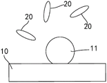
After the metal nanoparticles are formed, primer modification can be accomplished by directly subjecting the metal nanoparticles to primer immobilization treatment by thiolated oligonucleotides using thiol chemistry, for forming a biological sequencing chip substrate, as shown in fig. 6-8 in particular; in which fig. 6 completely reflects the process of primer fixing treatment, fig. 7 reflects the array substrate of nanoparticles and thiolated oligonucleotide before primer fixing treatment, and fig. 8 reflects the result of primer fixing treatment of the array substrate of nanoparticles based on fig. 7. As can be seen from FIGS. 6 to 8, the thiolated oligonucleotide 20 is bound to the metal nanoparticles 11 on the nanoparticle array substrate 10 after the primer immobilization process.
In addition to the above methods, the metal nanoparticles can be indirectly primer-modified by other surface functional groups reactive with the modified oligonucleotides to form a biological sequencing chip substrate.
After the metal nanoparticles are modified by the primers, the substrate can be used for bridging (bridge) or template walking (template walking) amplification. Since the primer region is discontinuous and is bounded by the metal nanoparticle boundaries, the cluster size is limited only by the size of the metal nanoparticles when over-amplified, and does not overgrow into large clusters. The clusters thus obtained are of uniform size and are not affected by inhomogeneities in the surface reactivity.
While embodiments of the invention have been described above, it is not limited to the applications set forth in the description and the embodiments, which are fully applicable in various fields of endeavor to which the invention pertains, and further modifications may readily be made by those skilled in the art, it being understood that the invention is not limited to the details shown and described herein without departing from the general concept defined by the appended claims and their equivalents.