Disclosure of Invention
In view of the above problems in the prior art, the present invention provides a porous film getter structure and a method for preparing the same, which can effectively increase the deposition area of a film and the adhesion of the film to a sidewall. The getter amount can be greatly increased, and the phenomena of falling off of the film, damage of devices and the like can be effectively avoided, so that the advantages of improving the internal vacuum degree of the electronic device, prolonging the service life, keeping high stability and the like are achieved.
In order to achieve the purpose, the invention adopts the following technical scheme:
the porous film getter structure comprises a wafer and a film getter, wherein the upper surface of the wafer is provided with a groove structure, the inner wall of the groove structure is of a porous structure, the film getter is arranged on the porous structure, and the porous structure is covered by the film getter.
Preferably, the wafer is provided with more than two groove structures, the surface of the wafer connected with the adjacent groove structures is a porous structure, the porous structure is provided with a film getter, and the film getter covers the porous structure.
Preferably, the bottom surfaces of the pores of the porous structure are provided with gold particles, and the thin-film getter covers the gold particles; the size of the gold particles is 20 nm-5 mu m.
Preferably, the groove structure has a trapezoidal, V-shaped or cross-section "
And (4) shape.
Preferably, the pore space and the inner wall of the groove structure are arranged at an angle; the angle is greater than 0 and less than 180 deg..
As a general inventive concept, the present invention also provides a method of making a porous, thin film getter structure, comprising the steps of:
s1, forming protective layers on the upper surface and the lower surface of the wafer, forming a graphical photoresist layer on the protective layer on the upper surface of the wafer, and taking the graphical photoresist layer as a mask to enable the protective layer on the upper surface of the wafer to be graphical and expose the surface area of the wafer to be etched;
s2, carrying out dry etching on the wafer by taking the patterned photoresist layer as a mask to form a groove structure, and then removing the patterned photoresist layer; or removing the patterned photoresist layer, and performing wet etching on the wafer by using the protective layer as a mask to form a groove structure;
s3, forming a patterned photoresist layer on the groove structure area of the upper surface of the wafer, and forming a photoresist layer on the upper surface of the wafer outside the groove structure area so as to form a patterned window on the inner wall of the groove or the inner wall of the groove structure area and the surface of the wafer;
s4, forming a gold film on the surface of the graphical window of the groove structure area;
s5, carrying out high-temperature annealing on the wafer plated with the gold film so as to enable the gold film to be converted into gold particles under the action of stress;
s6, carrying out wet etching on the wafer subjected to high-temperature annealing by using an etching solution, and etching the groove structure area into a porous structure under the catalytic action of gold;
and S7, evaporating a thin film getter on the upper surface of the wafer through a photoetching stripping process.
Preferably, in step S2, the number of the groove structures is one or more than two; when the number of the groove structures is more than two, each groove structure and the area connecting the adjacent groove structures form a groove structure area; when the number of the groove structures is more than two, the step S2 further includes removing the protection layer connecting the adjacent groove structures by etching after the groove structures are formed.
When the number of the groove structures is two or more, in step S3, a patterned photoresist layer is formed on the groove structure region of the upper surface of the wafer, and a patterned window is formed on the upper surface of the wafer outside the groove structure region, so as to form a patterned window on the inner wall of the groove in the groove structure region and the surface of the wafer.
Preferably, in step S2, dry etching is performed to form a cross section of "
The shape of the groove is a trapezoid or V-shaped groove formed by wet etching.
Preferably, in the step S5, the heat preservation temperature of the high-temperature annealing is 600-1000 ℃; the heat preservation time of the high-temperature annealing is 2-60 min; the heating rate of the high-temperature annealing is 5-25 ℃/min; the annealing rate of the high-temperature annealing is 5-25 ℃/min.
Preferably, in step S1, the protective layer is one or more metal films of Ti, Pt, and Cr; and plating a protective layer by adopting modes of magnetron sputtering, evaporation plating and the like.
Preferably, in step S6, the etching solution is a mixed etching solution of hydrofluoric acid and hydrogen peroxide; the temperature of the wet etching is 25-60 ℃.
Preferably, in the mixed corrosive liquid, the mass fraction of the hydrofluoric acid in the mixed corrosive liquid is 5-20%, and the H content is2O2The mass fraction of (A) is 5-30%.
Preferably, in step S4, the gold film has a thickness of 30 to 150 nm.
Step S4 specifically includes: and forming a gold film on the upper surface of the wafer through evaporation, deposition or sputtering, removing the patterned photoresist layer of the groove structure region and the photoresist layer on the upper surface of the wafer outside the groove structure region, forming the gold film on the patterned window of the groove structure region, and cleaning the wafer.
Preferably, in step S1, the wafer is a double-polished silicon wafer, and before the protective layer is plated, the method further includes performing inorganic cleaning and organic cleaning on the silicon wafer.
Preferably, in step S2, the groove structure has a trapezoidal, V-shaped or cross-section "
And (4) shape.<100>The silicon wafer with crystal face can be corroded along 110 crystal direction in the wet corrosion process, almost no corrosion is caused to 111 crystal face, the corrosion structure presents a slope face of 54.7 degrees, the whole structure can form a V shape or a trapezoid according to the size and the depth of a corrosion opening, and the V shape or the trapezoid can be formed under the dry etching condition "
The structure of a 'shaped groove deep cavity'.
A step of removing the passivation layer on the wafer surface is further included between steps S6 and S7 or after step S7; removal may be by etching.
In step S7, the thin film getter component generally has an alloy structure composed of several metals such as Zr, Co, Re, Zn, etc.
Compared with the prior art, the invention has the following beneficial effects:
1. according to the invention, the dry etching or wet etching is combined with the gold particle-assisted etching of the three-dimensional film getter structure, a porous structure can be prepared on the prepared groove structure to increase the deposition area of the film getter and the volume of the deposited getter, and the deposition area and the deposition volume are far larger than those of the existing three-dimensional concavo-convex body structure, so that the air suction performance and the service life of the film getter are effectively improved; the gold film deposited by the evaporation-stripping process can form uniformly distributed gold particles on the side wall and the base of the groove under the process condition of high-temperature rapid annealing, the annealed gold particles are utilized for carrying out an etching process, a uniformly distributed porous structure is etched on the side wall, the limitation of etching by directly depositing the gold particles is avoided, holes formed by etching, particularly holes in the side wall, can effectively increase the adhesiveness of the getter film, the side wall and the bottom substrate after the getter is deposited, and the phenomena that the getter falls off and a device is damaged are avoided.
2. According to the invention, the gold particles on the inner wall of the groove and the surface of the wafer are matched with corrosive liquid, holes with controllable diameters and sizes ranging from nanometer to several micrometers can be etched on the side wall and the surface of the wafer, and the size parameters of the porous structure can be regulated and controlled through the thickness setting of the gold-plated film and the setting of high-temperature annealing parameters, which are effects that dry etching and conventional wet processes are difficult to obtain, so that the method has great effects on maintaining the internal vacuum property of a high-vacuum electronic device and prolonging the service life; and the gold particles after high-temperature rapid annealing are distributed at uniform intervals, and an excessively dense and disordered structure can not be formed, so that the formed porous structure has good stability, and the phenomenon of fracture and collapse caused by excessive density can not occur.
Detailed Description
The invention is further described below with reference to the drawings and specific preferred embodiments of the description, without thereby limiting the scope of protection of the invention.
Aiming at the current situations that the traditional two-dimensional planar structure film getter has small deposition surface area, the side wall film of a three-dimensional structure has low adhesiveness, is easy to fall off and damage a device, the opening size of the side wall is difficult to control and the like, the invention designs the structure of the porous film getter which is etched by adopting gold particles for assisting, and the gold particles are etched on the cavity structure after dry etching, so that the deposition area of the film getter can be effectively increased, on the other hand, the porous structure on the side wall of the cavity can effectively increase the deposition area of the film and the adhesiveness between the film and the side wall, and the phenomena of falling off of the film, damage of the device and the like are effectively avoided. Thereby achieving the advantages of improving the internal vacuum degree of the electronic device, prolonging the service life, keeping high stability and the like.
The invention provides the following technical scheme:
and (4) performing inorganic cleaning and organic cleaning on the silicon wafer respectively by adopting a double-polished silicon wafer. And plating one or more metal films of protective layers Ti, Pt and Cr on the upper surface and the lower surface of the double-polished silicon wafer by adopting modes of magnetron sputtering, evaporation plating and the like to be used as the protective layers, then patterning the protective layers, namely coating photoresist on the surface of the wafer and patterning, and etching to remove the surface protective layers.
Regular and ordered vertical, trapezoidal or V-shaped grooves are etched on the surface of the wafer by adopting a dry etching or wet etching process.
And sputtering or evaporating a layer of gold film on the concave or V-shaped cavity structure of the wafer by adopting a stripping process.
And (2) carrying out a high-temperature rapid annealing process on the wafer after the gold film is plated, wherein the wafer can be rapidly heated to 600-1000 ℃ at a heating rate of 5-25 ℃/min and is subjected to the rapid annealing process after being kept for 2-60 min, the annealing rate (cooling rate) is 5-25 ℃/min, the gold film can be converted into gold particles with nanometer or micron size under the action of stress, and the gold particles are uniformly distributed on the side wall and the substrate of the cavity structure. The melting points of the protective layers Ti and Pt are above 1600 ℃ and are not influenced by annealing;
configuration of HF and H2O2、H2And carrying out wet etching on the side wall and the substrate area of the cavity by using the mixed etching solution of O in combination with the uniformly distributed gold particles, and etching a porous structure on the side wall and the bottom of the cavity.
And carrying out an evaporation process of the film getter on the area of the wafer needing film coating.
Aiming at the current situations that the traditional getter with a two-dimensional planar structure film has small deposition surface area, the side wall film with a three-dimensional structure has low adhesiveness, is easy to fall off and damage devices, the opening size of the side wall is difficult to control and the like, the invention designs a gold film annealing process to prepare gold particles uniformly distributed on the side wall and the substrate, and the gold particles are matched with HF and H2O2The solution assisted etching porous film getter structure, and the gold particle assisted etching on the cavity side wall and the substrate structure after dry or wet etching has the following three advantages:
firstly, the method comprises the following steps: the combination of two etching processes can effectively increase the deposition area of the film getter, and the deposition area is far larger than that of the original three-dimensional concave-convex body structure.
Secondly, the method comprises the following steps: in the process of the rapid annealing process, due to the action of stress, gold particles which are uniformly distributed can be formed on the side wall after the annealing is finished, and a porous structure which is uniformly distributed can be etched on the side wall by matching with corrosive liquid, so that the limitation of directly depositing the gold particles for etching is avoided. And the porous structure on the side wall of the cavity can effectively increase the adhesion between the film and the side wall, and effectively avoid the phenomena of film falling, device damage and the like.
Thirdly, the method comprises the following steps: the sizes of the diameters of the holes etched on the side wall and the substrate are controllable, the sizes of the holes can be designed and adjusted in the previous gold-plated film process stage, the distribution intervals of the gold particles subjected to high-temperature rapid annealing are uniform, and an excessively dense and disordered structure cannot be formed, so that the formed porous structure cannot be broken and collapsed due to excessive density.
According to the invention, the three-dimensional groove or V-shaped cavity structure is secondarily processed by adopting the gold film high-temperature rapid annealing to form gold particles matched with corrosive liquid, so that the porous structure of the film getter is formed, and the advantages of improving the internal vacuum degree of an electronic device, prolonging the service life, keeping high stability and the like can be achieved.
Example 1
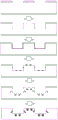
A porous film getter structure comprises a wafer and a film getter, as shown in figure 1, wherein the upper surface of the wafer is provided with a plurality of groove structures, the inner walls of the groove structures are all porous structures, the surface of the wafer connected with the adjacent groove structures is also provided with the porous structures, the porous structures are provided with the film getter, and the film getter covers the porous structures.
Gold particles are arranged on the bottom surfaces of the pores of the porous structure, and the thin film getter covers the gold particles. The grain diameter of the gold particles is between tens of nanometers and several micrometers, and can be adjusted according to the required structure size of the film getter.
The section of the groove structure is "
And (4) shape.
The specific preparation process diagram of the porous film getter structure, namely the manufacture of the capping silicon wafer, is shown in fig. 2, and comprises the following steps:
and S1, performing inorganic cleaning and organic cleaning on the silicon wafer respectively by adopting a double-polishing silicon wafer. Plating protective layers Ti (20-100 nm) and Pt (200-500 nm) on the front and back surfaces of the wafer, forming a graphical photoresist layer on the protective layer on the upper surface of the wafer, taking the graphical photoresist layer as a mask, then etching, and graphing the protective layer on the upper surface of the wafer to expose a wafer area needing etching;
s2, carrying out dry etching on the wafer by taking the patterned photoresist layer as a mask to form a plurality of orderly groove structures with cross sections "
Removing the photoresist layer, and removing the protective layer on the surface of the wafer connected with the adjacent grooves by etching;
s3, exposing the area needing to be coated with the film getter by adopting glue spraying and stripping processes, namely forming a patterned photoresist layer in the groove structure area of the upper surface of the wafer (namely the inner wall of the groove structure and the surface of the wafer connected with the adjacent groove structure), and forming a photoresist layer on the upper surface of the wafer outside the groove structure area to form a patterned window;
s4, forming a gold film on the upper surface of the wafer and the inner wall of the groove structure region through evaporation, stripping off the patterned photoresist layer of the groove structure region and the photoresist layer on the upper surface of the wafer outside the groove structure region, forming a patterned gold film on the patterned window (the inner wall of the groove structure and the patterned window of the connecting part connecting the adjacent groove structures) of the groove structure region, and cleaning the wafer;
s5, carrying out high-temperature annealing on the wafer plated with the gold film to convert the gold film into gold particles under the action of stress;
s6, carrying out wet etching on the wafer subjected to high-temperature annealing by using an etching solution, and etching the groove structure area into a porous structure under the catalytic action of gold; in the process, the thickness of the gold film evaporation coating determines the grain size after annealing, the size of the gold grains determines the diameter of the porous structure, and the thickness of the gold film coating can be changed according to the requirement of the actual process.
And S7, evaporating a thin film getter on the upper surface of the wafer through a photoetching stripping process.
In step S2, the dry etching condition is SF6And C4F8And carrying out deep silicon etching on the wafer cavity structure by using the gas to etch a groove structure. The specific etching parameters are as follows: chamber pressure 40mTorr, source power 2500W, C4F8Gas volume flow of 200cm3/min,SF6Gas volume flow of 300cm3/min。
In the step S5, the wafer after being plated with the gold film is subjected to a high temperature rapid annealing process, which includes rapidly heating the wafer to a temperature of 600-1000 ℃ at a heating rate of 5-25 ℃/min for a time period of 2-60 min, and performing a rapid annealing process at a cooling rate of 5-25 ℃/min, wherein the gold film is converted into gold particles of micron-sized size under the action of stress and is uniformly distributed on the sidewall and the substrate of the cavity structure. The melting points of the protective layers Ti and Pt are above 1600 ℃ and are not affected by annealing.
In step S6, preparing a mixed etching solution of hydrofluoric acid and hydrogen peroxide, and performing wet etching on the annealed wafer by using the prepared mixed etching solution, wherein the essence of the etching process is to use H2O2the/HF etching liquid and the gold particles form an electrochemical corrosion system, the gold particles are used as reaction catalysts to dig holes downwards, and the diameter and the depth of the holes are determined by the concentration of the etching liquid, the reaction temperature and the diameter of the gold particles.
The corrosive liquid is a mixed corrosive liquid of hydrofluoric acid and hydrogen peroxide; in the mixed corrosive liquid, the mass fraction of hydrofluoric acid is 5-20%, and H is2O2The mass fraction of (A) is 5-30%; the reaction temperature of the corrosion was 40 ℃.
In step S4, the thickness of the gold film is 3-150 nm.
In step S7, a photolithography stripping process is used to evaporate a film getter on the top of the wafer, and the process includes spraying glue, exposing, developing, coating and stripping. The film evaporation process can be sputtering or evaporation, and the components of the film getter generally have an alloy structure consisting of several metals such as Zr, Co, Re, Zn and the like.
Example 2
A porous film getter structure is shown in figure 3 and comprises a wafer and a film getter, wherein the upper surface of the wafer is provided with a groove structure, the inner walls of the groove structure are all porous structures, the film getter is arranged on the porous structures, and the porous structures are covered by the film getter.
Gold particles are arranged on the bottom surfaces of the pores of the porous structure, and the thin film getter covers the gold particles. The particle size of the gold particles is tens of nanometers to several micrometers; the cross section of the groove structure is V-shaped.
The wafer is provided with more than two groove structures, the surface of the wafer connected with the adjacent groove structures is of a porous structure, a film getter is arranged on the porous structure, and the porous structure is covered by the film getter.
The specific preparation process diagram of the porous film getter structure, namely the manufacture of the capping silicon wafer, is shown in fig. 4, and comprises the following steps:
and S1, performing inorganic cleaning and organic cleaning on the silicon wafer respectively by adopting a double-polishing silicon wafer. Plating protective layers Ti (20-100 nm) and Pt (200-500 nm) on the front and back surfaces of the wafer, forming a graphical photoresist layer on the protective layer on the upper surface of the wafer, etching by taking the graphical photoresist layer as a mask, and patterning the protective layer on the upper surface of the wafer to expose a surface area of the wafer to be etched;
s2, removing the patterned photoresist layer, performing wet etching on the wafer by taking the patterned protective layer as a mask to form a plurality of orderly groove structures, wherein the cross sections of the groove structures are V-shaped, and removing the protective layer on the surface of the wafer connected with the adjacent grooves by etching;
s3, exposing the area needing to be coated with the film getter by adopting glue spraying and stripping processes, namely forming a patterned photoresist layer in the groove structure area of the upper surface of the wafer (namely the inner wall of the groove structure and the surface of the wafer connected with the adjacent groove structure), and forming a photoresist layer on the upper surface of the wafer outside the groove structure area to form a patterned window;
s4, forming a gold film on the upper surface of the wafer through evaporation, stripping and removing the patterned photoresist layer of the groove structure region and the photoresist layer on the upper surface of the wafer outside the groove structure region, forming a patterned gold film on the patterned window of the groove structure region, and cleaning the wafer;
s5, carrying out high-temperature annealing on the wafer plated with the gold film to convert the gold film into gold particles under the action of stress;
s6, carrying out wet etching on the wafer subjected to high-temperature annealing by using an etching solution, and etching the groove structure area into a porous structure under the catalytic action of gold; in the process, the thickness of the gold film evaporation coating determines the grain size after annealing, the size of the gold grains determines the diameter of the porous structure, and the thickness of the gold film coating can be changed according to the requirement of the actual process.
And S7, evaporating a thin film getter on the upper surface of the wafer through a photoetching stripping process.
In step S2, wet etching is performed at 25-80 ℃ by using TMAH (25% concentration) or KOH solution (10-30% concentration), and the specific etching conditions may be changed according to actual process requirements.
In the step S5, the wafer after being plated with the gold film is subjected to a high temperature rapid annealing process, which includes rapidly heating the wafer to a temperature of 600-1000 ℃ at a heating rate of 5-25 ℃/min for a time period of 2-60 min, and performing a rapid annealing process at a cooling rate of 5-25 ℃/min, wherein the gold film is converted into gold particles of micron-sized size under the action of stress and is uniformly distributed on the sidewall and the substrate of the cavity structure. The melting points of the protective layers Ti and Pt are above 1600 ℃ and are not affected by annealing.
In step S6, preparing a mixed etching solution of hydrofluoric acid and hydrogen peroxide to perform wet etching on the annealed wafer, wherein the essence of the etching process is to use H2O2the/HF etching liquid and the gold particles form an electrochemical corrosion system, the gold particles are used as reaction catalysts to dig holes downwards, and the diameter and the depth of the holes are determined by the concentration of the etching liquid, the reaction temperature and the diameter of the gold particles.
The corrosive liquid is a mixed corrosive liquid of hydrofluoric acid and hydrogen peroxide; in the mixed corrosive liquid, the mass fraction of hydrofluoric acid is 5 to c20%,H2O2The mass fraction of (A) is 5-30%; the reaction temperature of the corrosion was 40 ℃.
In step S4, the thickness of the gold film is 30-150 nm.
In step S7, a photolithography stripping process is used to evaporate a film getter on the top of the wafer, and the process includes spraying glue, exposing, developing, coating and stripping. The film evaporation process can be sputtering or evaporation, and the components of the film getter generally have an alloy structure consisting of several metals such as Zr, Co, Re, Zn and the like.
The method adopts double-polished silicon wafers, a substrate of a vertical or V-shaped groove is prepared on the surface of a wafer by adopting a dry etching process or a wet etching process, a gold film with a certain thickness is plated, and the thickness of the gold film directly influences the size of gold particles and the diameter of side wall and substrate etching holes. The uniform gold film is prepared with uniformly distributed gold particles by adopting a rapid annealing process, the side wall and the bottom of the groove attached with the gold particles are corroded by using a HF and H2O2 mixed solution to form a porous structure, the diameter and the size of the holes are controllable, and the sizes of the holes can be completely designed and regulated in the previous gold-plating film process stage. The size of the gold particles after annealing can be adjusted by adjusting the thickness of the gold film, so that the size of the porous structure can be adjusted to adapt to the structural size required by the deposited film getter. In addition, the porous structure not only effectively increases the deposition surface of the film getter, but also enhances the adhesion between the film getter and the side wall, prolongs the service life of the MEMS chip under high vacuum, and prevents the getter from falling off during the use of the device, and the device from being out of order, damaged and the like.
The three-dimensional film getter structure is etched by the aid of gold particles, a porous structure can be continuously prepared on the originally prepared groove or V-shaped cavity structure to increase the deposition area of the film getter, the amount of the deposited getter can be increased, and therefore the air suction performance and the service life of the film getter are improved. The gold film can form uniformly distributed gold particles on the side wall and the substrate of the cavity under the process condition of high-temperature rapid annealing, the gold particles on the side wall and the substrate of the wall can etch holes with controllable diameters ranging from nanometer to several micrometers on the side wall and the substrate by matching with corrosive liquid, and the size parameters of the porous structure can be regulated and controlled by the thickness setting of the gold-plated film and the setting of high-temperature annealing parameters, which is an advantage difficult to realize by dry etching and common wet process, so that the method has great effects on maintaining the internal vacuum property of a high-vacuum electronic device and prolonging the service life.
And the annealed gold particles are used for etching process, holes formed by etching, particularly holes on the side wall can effectively increase the adhesion of the getter film, the side wall and the bottom substrate after the getter is deposited, and the phenomena that the getter falls off and a device is damaged are avoided.
The foregoing is merely a preferred embodiment of the invention and is not intended to limit the invention in any manner. Although the present invention has been described with reference to the preferred embodiments, it is not intended to be limited thereto. Those skilled in the art can make many possible variations and modifications to the disclosed embodiments, or equivalent modifications, without departing from the spirit and scope of the invention, using the methods and techniques disclosed above. Therefore, any simple modification, equivalent replacement, equivalent change and modification made to the above embodiments according to the technical essence of the present invention are still within the scope of the protection of the technical solution of the present invention.