CN113593473A - Display panel driving circuit and driving method - Google Patents
Display panel driving circuit and driving method Download PDFInfo
- Publication number
- CN113593473A CN113593473A CN202110895446.5A CN202110895446A CN113593473A CN 113593473 A CN113593473 A CN 113593473A CN 202110895446 A CN202110895446 A CN 202110895446A CN 113593473 A CN113593473 A CN 113593473A
- Authority
- CN
- China
- Prior art keywords
- node
- switch tube
- switching tube
- scan line
- electrically connected
- Prior art date
- Legal status (The legal status is an assumption and is not a legal conclusion. Google has not performed a legal analysis and makes no representation as to the accuracy of the status listed.)
- Granted
Links
Images


Classifications
-
- G—PHYSICS
- G09—EDUCATION; CRYPTOGRAPHY; DISPLAY; ADVERTISING; SEALS
- G09G—ARRANGEMENTS OR CIRCUITS FOR CONTROL OF INDICATING DEVICES USING STATIC MEANS TO PRESENT VARIABLE INFORMATION
- G09G3/00—Control arrangements or circuits, of interest only in connection with visual indicators other than cathode-ray tubes
- G09G3/20—Control arrangements or circuits, of interest only in connection with visual indicators other than cathode-ray tubes for presentation of an assembly of a number of characters, e.g. a page, by composing the assembly by combination of individual elements arranged in a matrix no fixed position being assigned to or needed to be assigned to the individual characters or partial characters
- G09G3/22—Control arrangements or circuits, of interest only in connection with visual indicators other than cathode-ray tubes for presentation of an assembly of a number of characters, e.g. a page, by composing the assembly by combination of individual elements arranged in a matrix no fixed position being assigned to or needed to be assigned to the individual characters or partial characters using controlled light sources
- G09G3/30—Control arrangements or circuits, of interest only in connection with visual indicators other than cathode-ray tubes for presentation of an assembly of a number of characters, e.g. a page, by composing the assembly by combination of individual elements arranged in a matrix no fixed position being assigned to or needed to be assigned to the individual characters or partial characters using controlled light sources using electroluminescent panels
- G09G3/32—Control arrangements or circuits, of interest only in connection with visual indicators other than cathode-ray tubes for presentation of an assembly of a number of characters, e.g. a page, by composing the assembly by combination of individual elements arranged in a matrix no fixed position being assigned to or needed to be assigned to the individual characters or partial characters using controlled light sources using electroluminescent panels semiconductive, e.g. using light-emitting diodes [LED]
-
- G—PHYSICS
- G09—EDUCATION; CRYPTOGRAPHY; DISPLAY; ADVERTISING; SEALS
- G09G—ARRANGEMENTS OR CIRCUITS FOR CONTROL OF INDICATING DEVICES USING STATIC MEANS TO PRESENT VARIABLE INFORMATION
- G09G2320/00—Control of display operating conditions
- G09G2320/02—Improving the quality of display appearance
- G09G2320/0233—Improving the luminance or brightness uniformity across the screen
Landscapes
- Engineering & Computer Science (AREA)
- Physics & Mathematics (AREA)
- Computer Hardware Design (AREA)
- General Physics & Mathematics (AREA)
- Theoretical Computer Science (AREA)
- Control Of Indicators Other Than Cathode Ray Tubes (AREA)
Abstract
The application provides a display panel driving circuit and a driving method, relates to the technical field of display, solves the problem of uneven display brightness, and comprises a first switch tube, a second switch tube, a third switch tube, a fourth switch tube, a fifth switch tube, a sixth switch tube, a first capacitor, a second capacitor and a light-emitting device, wherein the first switch tube and the second switch tube are used for controlling the first switch tube and the second switch tube, the third switch tube, the fourth switch tube, the fifth switch tube and the sixth switch tube are used as driving switch tubes in the driving circuit and are connected to the first scanning line, the second scanning line, the third scanning line, the data signal line, the reset signal line and the control signal line, so that the threshold voltage of the driving switch tubes can be effectively compensated, the problem of unstable current flowing through the light-emitting device caused by threshold voltage drift is solved, the uniformity of the light-emitting brightness of the light-emitting device is ensured, and the display effect of pictures is improved.
Description
Technical Field
The present application relates to the field of display technologies, and in particular, to a display panel driving circuit and a driving method.
Background
The Micro semiconductor light emitting diode (Micro-LED) is a current driving type light emitting device, when the Micro-LED employs Active drive (AM), a conventional pixel (pixel) driving architecture of the Micro-LED backplane is a structure of 2 Thin Film field effect transistors (TFTs) and 1 capacitor (C), as shown in fig. 1, i.e., a 2T1C architecture, as shown in fig. 2, a driving manner of the 2T1C structure is that when a scanning signal WR is at a VGH high potential, T1 is turned on, a data signal Vdata signal is written into one end of Cst, and when the WR is at a VGL low potential, T1 is turned off, and the Cst stores the Vdata potential until T1 is turned on again to write a new Vdata signal. For the 2T1C architecture, the Vdata signal writesIn the moment VDD-LED-T2-VSS path, current flows, and the value of the current flowing through the LED is ILED 1/2K (VGS-Vth)2The LED is lighted, and different gray scales are displayed according to different Vdata values.
According to the formula ILED 1/2K (VGS-Vth)2It can be seen that, as shown in fig. 1, the current value of the LED (i.e. the brightness of the LED) is related to the VGS value and Vth of the driving transistor T2, because a plurality of pixels are arranged in an array in the backplane and limited by the manufacturing level of the TFT backplane, the threshold voltage (Vth) of the driving transistor T2 in each Pixel on the backplane cannot be guaranteed to be completely consistent, and the driving transistor T2 is continuously biased in the forward direction, which causes the Vth of the driving transistor T2 to drift, and under the condition that other signals are input in the same direction, the current flowing through the LEDs in different pixels will also be different, which causes different brightness and affects the display effect.
Disclosure of Invention
The application provides a display panel driving circuit and a driving method which can compensate the difference of threshold voltages between driving tubes in a back panel driving circuit, reduce the difference of currents flowing through light emitting devices in different pixel units and balance the display brightness of the light emitting devices.
In one aspect, the present application provides a display panel driving circuit, including a first switching tube, a second switching tube, a third switching tube, a fourth switching tube, a fifth switching tube, a sixth switching tube, a first capacitor, a second capacitor, and a light emitting device;
the grid electrode of the first switch tube is electrically connected with a first node, the source electrode of the first switch tube is electrically connected with a second node, and the drain electrode of the first switch tube is electrically connected with a third node;
a grid electrode of the second switching tube is electrically connected with a first scanning line, a source electrode of the second switching tube is electrically connected with the second node, and a drain electrode of the second switching tube is electrically connected with the first node;
the grid electrode of the third switching tube is electrically connected with a second scanning line, the source electrode of the third switching tube is electrically connected with a reset signal line, and the drain electrode of the third switching tube is electrically connected with the third node;
a grid electrode of the fourth switching tube is electrically connected to the first scanning line, a source electrode of the fourth switching tube is electrically connected to a fourth node, and a drain electrode of the fourth switching tube is electrically connected to the reset signal line;
a gate of the fifth switching tube is electrically connected with a third scanning line, a source of the fifth switching tube is electrically connected with the fourth node, and a drain of the fifth switching tube is electrically connected with a data signal line;
a grid electrode of the sixth switching tube is electrically connected with a control signal wire, a source electrode of the sixth switching tube is electrically connected with the second node, and a drain electrode of the fifth switching tube is electrically connected with a power supply anode;
a first end of the first capacitor is electrically connected to the first node, and a second end of the first capacitor is electrically connected to the fourth node;
a first end of the second capacitor is electrically connected to the first node, and a second end of the second capacitor is electrically connected to the third node;
and the anode of the light-emitting device is electrically connected to the third node, and the cathode of the light-emitting device is electrically connected to the negative electrode of the power supply.
In one possible implementation manner of the present application, the combination of the first scan line, the second scan line, the third scan line, and the control signal line sequentially corresponds to a reset phase, a compensation phase, a data writing phase, and a light emitting phase.
In one possible implementation manner of the present application, in the reset stage, the first scan line is at a high level, the second scan line is at a high level, the third scan line is at a low level, and the control signal line is at a high level.
In a possible implementation manner of the present application, in the reset stage, the first switching tube, the second switching tube, the third switching tube, the fourth switching tube, and the sixth switching tube are all in an on state, and the fifth switching tube is in an off state.
In one possible implementation manner of the present application, in the compensation stage, the first scan line is at a high level, the second scan line is at a high level, the third scan line is at a low level, and the control signal line is at a low level.
In a possible implementation manner of the present application, in the compensation stage, the first switching tube, the second switching tube, the third switching tube, and the fourth switching tube are all in an on state, and the fifth switching tube and the sixth switching tube are all in an off state.
In a possible implementation manner of the present application, in the data writing stage, the first scan line is at a low level, the second scan line is at a high level, the third scan line is at a high level, and the control signal line is at a low level.
In a possible implementation manner of the present application, in the data writing stage, the first switch tube, the third switch tube, and the fifth switch tube are all in an on state, and the second switch tube, the fourth switch tube, and the sixth switch tube are all in an off state.
In one possible implementation manner of the present application, in the light emitting stage, the first scan line is at a low level, the second scan line is at a low level, the third scan line is at a low level, and the control signal line is at a high level.
In a possible implementation manner of the present application, in the light emitting stage, the first switching tube and the sixth switching tube are all in an on state, and the second switching tube, the third switching tube, the fourth switching tube and the fifth switching tube are all in an off state.
In another aspect, the present application provides a driving method, including:
providing a display panel driving circuit;
entering a reset phase, wherein the first scan line provides a high level, the second scan line provides a high level, the control signal line provides a high level, the first switch tube, the second switch tube, the third switch tube, the fourth switch tube and the sixth switch tube are all in an on state, the third scan line provides a low level, the fifth switch tube is in an off state, a positive power supply voltage is written into the first node, and a reset voltage is written into the third node and the fourth node;
entering a compensation phase, wherein the first scan line provides a high level, the second scan line provides a high level, the first switching tube, the second switching tube, the third switching tube and the fourth switching tube are all in an on state, the third scan line provides a low level, the control signal line provides a low level, the fifth switching tube and the sixth switching tube are all in an off state, the third node and the fourth node maintain a reset voltage, the voltage of the first node is changed to a first voltage V1, V1 is Vini + Vth, where Vini is the reset voltage, and Vth is the threshold voltage of the first switching tube;
entering a Data writing phase, wherein the first scan line provides a low level, the control signal line provides a low level, the second, fourth, and sixth switching tubes are all in an off state, the second scan line provides a high level, the third scan line provides a high level, the first, third, and fifth switching tubes are all in an on state, the third node maintains a reset voltage, the fourth node writes a Data signal while the first capacitor couples the Data signal to the first node, a voltage of the first node changes to a second voltage V2, V2 is Vini + Vth + (Data-Vini) ([ C1/(C1+ C2) ], where Vini is the reset voltage, Vth is a threshold voltage of the first switching tube, Data is the Data signal, and C1 is a capacitance value of the first capacitor, c2 is the capacitance of the second capacitor;
entering a light emitting phase, wherein the first scan line provides a low level, the second scan line provides a low level, the third scan line provides a low level, the control signal line provides a high level, the first switch tube and the sixth switch tube are all in an on state, the second switch tube, the third switch tube and the fourth switch tube and the fifth switch tube are all in an off state, a positive power supply voltage is written into the second node and the third node, a second voltage V2 of the first node is consumed, a second voltage V2 includes a threshold voltage of the first switch tube, and the light emitting device emits light.
According to the driving circuit, the first switch tube, the second switch tube, the third switch tube, the fourth switch tube, the fifth switch tube and the sixth switch tube are used as the driving switch tube in the driving circuit, and the first scanning line, the second scanning line, the third scanning line, the data signal line, the reset signal line and the control signal line are connected, so that the threshold voltage of the driving switch tube can be effectively compensated, the problem that the current flowing through the light-emitting device caused by threshold voltage drift is unstable is solved, the uniformity of the light-emitting brightness of the light-emitting device is ensured, and the display effect of a picture is improved.
Drawings
In order to more clearly illustrate the technical solutions in the embodiments of the present application, the drawings needed to be used in the description of the embodiments are briefly introduced below, and it is obvious that the drawings in the following description are only some embodiments of the present invention, and it is obvious for those skilled in the art to obtain other drawings based on these drawings without creative efforts.
Fig. 1 is a circuit diagram of a conventional display panel driving circuit having a 2T1C structure;
fig. 2 is a timing diagram of a conventional display panel driving circuit having a 2T1C structure;
fig. 3 is a circuit diagram of a display panel driving circuit with a 6T2C structure in the embodiment of the present application;
FIG. 4 is a timing diagram of a display panel driving circuit with a 6T2C structure according to an embodiment of the present invention;
FIG. 5 is a schematic diagram of step 102 of the driving method in the embodiment of the present application;
fig. 6 is a schematic diagram of step 103 of the driving method in the embodiment of the present application;
FIG. 7 is a schematic diagram of step 104 of the driving method in the embodiment of the present application;
fig. 8 is a schematic diagram of step 105 of the driving method in the embodiment of the present application.
Detailed Description
The technical solutions in the embodiments of the present application will be clearly and completely described below with reference to the drawings in the embodiments of the present application, and it is obvious that the described embodiments are only a part of the embodiments of the present invention, and not all of the embodiments. All other embodiments, which can be derived by a person skilled in the art from the embodiments given herein without making any creative effort, shall fall within the protection scope of the present invention.
In the description of the present invention, it is to be understood that the terms "first", "second" and the like are used for descriptive purposes only and are not to be construed as indicating or implying relative importance or implying any number of technical features indicated. Thus, features defined as "first", "second", may explicitly or implicitly include one or more of the described features. In the description of the present invention, "a plurality" means two or more unless specifically defined otherwise.
In this application, the word "exemplary" is used to mean "serving as an example, instance, or illustration. Any embodiment described herein as "exemplary" is not necessarily to be construed as preferred or advantageous over other embodiments. The following description is presented to enable any person skilled in the art to make and use the invention. In the following description, details are set forth for the purpose of explanation. It will be apparent to one of ordinary skill in the art that the present invention may be practiced without these specific details. In other instances, well-known structures and processes are not shown in detail to avoid obscuring the description of the invention with unnecessary detail. Thus, the present invention is not intended to be limited to the embodiments shown, but is to be accorded the widest scope consistent with the principles and features disclosed herein.
Embodiments of the present invention provide a display panel driving circuit and a driving method thereof, which are described in detail below.
As shown in fig. 3, which is a schematic structural diagram of an embodiment of a display panel driving circuit in an embodiment of the present application, the driving circuit includes a first switching tube T1, a second switching tube T2, a third switching tube T3, a fourth switching tube T4, a fifth switching tube T5, a sixth switching tube T6, a first capacitor C1, a second capacitor C2, and a light emitting device LED;
the gate of the first switch tube T1 is electrically connected to a first node Vg, the source of the first switch tube T1 is electrically connected to a second node Vn, and the drain of the first switch tube T1 is electrically connected to a third node Vs;
the gate of the second switch tube T2 is electrically connected to the first Scan line Scan1, the source of the second switch tube T2 is electrically connected to the second node Vn, and the drain of the second switch tube T2 is electrically connected to the first node Vg;
the gate of the third transistor T3 is electrically connected to the second Scan line Scan2, the source of the third transistor T3 is electrically connected to the reset signal line Vini, and the drain of the third transistor T3 is electrically connected to the third node Vs;
the gate of the fourth switching tube T4 is electrically connected to the first Scan line Scan1, the source of the fourth switching tube T4 is electrically connected to the fourth node Va, and the drain of the fourth switching tube T4 is electrically connected to the reset signal line Vini;
a gate of the fifth switching tube T5 is electrically connected to a third Scan line Scan3, a source of the fifth switching tube T5 is electrically connected to the fourth node Va, and a drain of the fifth switching tube T5 is electrically connected to a Data signal line Data;
a gate of the sixth switching tube T6 is electrically connected to the control signal line Em, a source of the sixth switching tube T6 is electrically connected to the second node Vn, and a drain of the fifth switching tube T5 is electrically connected to the positive power supply VDD;
a first end of the first capacitor C1 is electrically connected to the first node Vg, and a second end of the first capacitor C1 is electrically connected to the fourth node Va;
a first end of the second capacitor C2 is electrically connected to the first node Vg, and a second end of the second capacitor C2 is electrically connected to the third node Vs;
the anode of the light emitting device LED is electrically connected to the third node Vs, and the cathode of the light emitting device LED is electrically connected to the power supply cathode Vss.
In the application, a first switch tube T1, a second switch tube T2, a third switch tube T3, a fourth switch tube T4, a fifth switch tube T5 and a sixth switch tube T6 are used as driving switch tubes in a driving circuit, and a first scanning line Scan1, a second scanning line Scan2, a third scanning line Scan3, a Data signal line Data, a reset signal line Vini and a control signal line Em are connected, so that the threshold voltage of the driving switch tubes can be effectively compensated, the problem of unstable current flowing through a light-emitting device LED caused by threshold voltage drift is solved, the uniformity of the light-emitting device LED light-emitting brightness is ensured, and the display effect of a picture is improved.
Specifically, the display panel driving circuit of the embodiment adopts a 6T2C architecture, the first switch tube T1 may adopt a Thin Film Transistor (TFT), or may adopt a Metal-Oxide-Semiconductor Field-Effect Transistor (MOSFET), the second switch tube T2, the third switch tube T3, the fourth switch tube T4, the fifth switch tube T5, and the sixth switch tube T6 may all adopt TFT tubes, or may adopt other types of switch tubes according to specific situations. In this embodiment, TFT transistors are used for the first switching transistor T1, the second switching transistor T2, the third switching transistor T3, the fourth switching transistor T4, the fifth switching transistor T5 and the sixth switching transistor T6.
The first switch transistor T1 is used as a driving TFT transistor for driving the light emitting device LED to emit light in the display panel driving circuit, and the display panel driving circuit can compensate the threshold voltage of the driving TFT, i.e., the first switch transistor T1. The first Scan line Scan1, the second Scan line Scan2, the third Scan line Scan3, the reset signal line Vini, and the control signal line Em are all generated by an external timing controller.
In another embodiment of the present application, as shown in fig. 4, the combination of the first Scan line Scan1, the second Scan line Scan2, the third Scan line Scan3 and the control signal line Em sequentially corresponds to a reset phase, a compensation phase, a data writing phase and a light emitting phase. The potential changes of the first node Vg, the third node Vs, and the fourth node Va in the reset phase, the compensation phase, the data writing phase, and the light emitting phase are specifically shown in table 1.
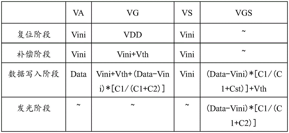
TABLE 1 Point voltages of nodes corresponding to stages of the driving circuit
The following is a detailed analysis of potential changes in the reset phase, compensation phase, data write phase, and light emission phase.
In another embodiment of the present application, during the reset phase, the first Scan line Scan1 is at a high level, the second Scan line Scan2 is at a high level, the control signal line Em is at a high level, the first switch transistor T1, the second switch transistor T2, the third switch transistor T3, the fourth switch transistor T4 and the sixth switch transistor T6 are all in an on state, the third Scan line Scan3 is at a low level, the fifth switch transistor T5 is in an off state, the first node Vg is written with the positive power voltage VDD, the third node Vs and the fourth node Va are written with the reset voltage Vini, and the light emitting device LED does not emit light because the fifth switch transistor T5 is in an off state.
In the compensation stage, the first Scan line Scan1 is at a high level, the second Scan line Scan2 is at a high level, the first switch transistor T1, the second switch transistor T2, the third switch transistor T3 and the fourth switch transistor T4 are all in an on state, the third Scan line Scan3 is at a low level, the control signal line Em is at a low level, the fifth switch transistor T5 and the sixth switch transistor T6 are all in an off state, the third node Vs and the fourth node Va maintain the reset voltage Vini, the voltage of the first node Vg is changed to a first voltage V1, and V1 is Vini + Vth, where Vini is the reset voltage Vini and Vth is the threshold voltage Vth of the first switch transistor T1.
Specifically, in the compensation phase, at the moment that the sixth switching tube T6 is turned off, the power supply positive voltage VDD written in the first node Vg in the reset phase starts to discharge until the gate-source voltage difference of the first switching tube T1 is equal to the threshold voltage Vth of the first switching tube T1, and at the same time, the first switching tube T1 is turned off, the voltage of the first node Vg is the sum of the drain voltage (i.e., the reset voltage Vini) of the first switching tube T1 and the threshold voltage Vth of the first switching tube T1, and the voltage of the first node Vg does not change any more, and at this moment, the potential voltage of the first node Vg includes the threshold voltage Vth information of the first switching tube T1, and the light emitting device LED does not emit light because the fifth switching tube T5 and the sixth switching tube T6 are both in the off state.
In the Data writing phase, the first Scan line Scan1 is at a low level, the control signal line Em is at a low level, the second switch T2, the fourth switch T4 and the sixth switch T6 are all in an off state, the second Scan line Scan2 is at a high level, the third Scan line Scan3 is at a high level, the first switch T1, the third switch T3 and the fifth switch T5 are all in an on state, the third node Vs maintains a reset voltage Vini, the fourth node Va writes a Data signal, and since the first node Vg potential is in a floating state, the first capacitor C1 couples the Data signal to the first node Vg, it can be known from the capacitive coupling principle that the voltage of the first node Vg changes to the second voltage V2, V2 is Vini + Data + (Data-Vini) [ C1/(C1+ C2, where Vini is the reset voltage V1, the Data threshold voltage of the first switch T1 is the Data threshold voltage of the Data switch 1, and the Data signal 1 is the Data switch 1, c1 is the capacitance of the first capacitor C1, and C2 is the capacitance of the second capacitor C2.
In the light emitting stage, the first Scan line Scan1 is at a low level, the second Scan line Scan2 is at a low level, the third Scan line Scan3 is at a low level, the control signal line Em is at a high level, the first switch transistor T1 and the sixth switch transistor T6 are all in an on state, the second switch transistor T2, the third switch transistor T3, the fourth switch transistor T4 and the fifth switch transistor T5 are all in an off state, the second node Vn and the third node Vs are written with the power supply positive voltage VDD, the second voltage V2 of the first node Vg is consumed, the second voltage V2 includes the threshold voltage Vth information of the first switch transistor T1, and the light emitting device LED emits light to achieve the effect of compensating the threshold voltage Vth of the first switch transistor T1.
On the other hand, as shown in fig. 5 to 8, the present application provides a driving method based on the above-mentioned display panel driving circuit, the driving method includes steps 101 to 105:
101. providing a driving circuit such as a display panel;
the driving circuit comprises a first switch tube T1, a second switch tube T2, a third switch tube T3, a fourth switch tube T4, a fifth switch tube T5, a sixth switch tube T6, a first capacitor C1, a second capacitor C2 and a light-emitting device LED.
102. As shown in fig. 5, in the reset phase, the first Scan line Scan1 provides a high level, the second Scan line Scan2 provides a high level, the control signal line Em provides a high level, the first switch transistor T1, the second switch transistor T2, the third switch transistor T3, the fourth switch transistor T4 and the sixth switch transistor T6 are all in an on state, the third Scan line Scan3 provides a low level, the fifth switch transistor T5 is in an off state, the first node Vg is written with the power supply positive voltage VDD, and the third node Vs and the fourth node Va are written with the reset voltage Vini;
103. as shown in fig. 6, in the compensation phase, the first Scan line Scan1 provides a high level, the second Scan line Scan2 provides a high level, the first switch transistor T1, the second switch transistor T2, the third switch transistor T3 and the fourth switch transistor T4 are all in an on state, the third Scan line Scan3 provides a low level, the control signal line Em provides a low level, the fifth switch transistor T5 and the sixth switch transistor T6 are all in an off state, the third node Vs and the fourth node Va maintain a reset voltage Vini, and the voltage of the first node Vg changes to a first voltage V1 and a first voltage V1 Vini + Vth, where Vini is the reset voltage Vini and Vth is the threshold voltage Vth of the first switch transistor T1;
104. as shown in fig. 7, in the data writing phase, the first Scan line Scan1 provides a low level, the control signal line Em provides a low level, the second switch T2, the fourth switch T4 and the sixth switch T6 are all in the off state, the second Scan line Scan2 provides a high level, the third Scan line Scan3 provides a high level, the first switch T1, the third switch T3 and the fifth switch T5 are all in the on state, the third node Vs maintains the reset voltage Vini, the fourth node Va writes the data signal, meanwhile, the first capacitor C1 couples the Data signal to the first node Vg, the voltage of the first node Vg is changed to a second voltage V2, V2 is Vini + Vth + (Data-Vini) [ C1/(C1+ C2) ], wherein Vini is a reset voltage Vini, Vth is a threshold voltage Vth of the first switch transistor T1, Data is a Data signal, C1 is a capacitance value of the first capacitor C1, and C2 is a capacitance value of the second capacitor C2;
105. as shown in fig. 8, in the light emitting period, the first Scan line Scan1 provides a low level, the second Scan line Scan2 provides a low level, the third Scan line Scan3 provides a low level, the control signal line Em provides a high level, the first switch transistor T1 and the sixth switch transistor T6 are both in an on state, the second switch transistor T2, the third switch transistor T3, the fourth switch transistor T4 and the fifth switch transistor T5 are all in an off state, the second node Vn and the third node Vs write the power positive voltage VDD, the second voltage V2 of the first node Vg is consumed, the second voltage V2 includes the threshold voltage Vth of the first switch transistor T1, and the light emitting device LED emits light.
The foregoing describes in detail a display panel driving circuit and a driving method provided in the embodiments of the present application, and the principles and embodiments of the present invention are described herein by applying specific examples, and the description of the foregoing embodiments is only used to help understanding the method and the core idea of the present invention; meanwhile, for those skilled in the art, according to the idea of the present invention, there may be variations in the specific embodiments and the application scope, and in summary, the content of the present specification should not be construed as a limitation to the present invention.
Claims (11)
1. A display panel driving circuit is characterized by comprising a first switch tube, a second switch tube, a third switch tube, a fourth switch tube, a fifth switch tube, a sixth switch tube, a first capacitor, a second capacitor and a light-emitting device;
the grid electrode of the first switch tube is electrically connected with a first node, the source electrode of the first switch tube is electrically connected with a second node, and the drain electrode of the first switch tube is electrically connected with a third node;
a grid electrode of the second switching tube is electrically connected with a first scanning line, a source electrode of the second switching tube is electrically connected with the second node, and a drain electrode of the second switching tube is electrically connected with the first node;
the grid electrode of the third switching tube is electrically connected with a second scanning line, the source electrode of the third switching tube is electrically connected with a reset signal line, and the drain electrode of the third switching tube is electrically connected with the third node;
a grid electrode of the fourth switching tube is electrically connected to the first scanning line, a source electrode of the fourth switching tube is electrically connected to a fourth node, and a drain electrode of the fourth switching tube is electrically connected to the reset signal line;
a gate of the fifth switching tube is electrically connected with a third scanning line, a source of the fifth switching tube is electrically connected with the fourth node, and a drain of the fifth switching tube is electrically connected with a data signal line;
a grid electrode of the sixth switching tube is electrically connected with a control signal wire, a source electrode of the sixth switching tube is electrically connected with the second node, and a drain electrode of the fifth switching tube is electrically connected with a power supply anode;
a first end of the first capacitor is electrically connected to the first node, and a second end of the first capacitor is electrically connected to the fourth node;
a first end of the second capacitor is electrically connected to the first node, and a second end of the second capacitor is electrically connected to the third node;
and the anode of the light-emitting device is electrically connected to the third node, and the cathode of the light-emitting device is electrically connected to the negative electrode of the power supply.
2. The display panel driving circuit according to claim 1, wherein the first scan line, the second scan line, the third scan line, and the control signal line in combination correspond to a reset phase, a compensation phase, a data write phase, and a light emission phase in sequence.
3. The display panel drive circuit according to claim 2, wherein in the reset phase, the first scan line is at a high level, the second scan line is at a high level, the third scan line is at a low level, and the control signal line is at a high level.
4. The display panel driving circuit as claimed in claim 3, wherein in the reset phase, the first switching tube, the second switching tube, the third switching tube, the fourth switching tube and the sixth switching tube are all in an on state, and the fifth switching tube is in an off state.
5. The display panel driving circuit according to claim 2, wherein in the compensation phase, the first scan line is at a high level, the second scan line is at a high level, the third scan line is at a low level, and the control signal line is at a low level.
6. The display panel driving circuit as claimed in claim 5, wherein during the compensation phase, the first switch tube, the second switch tube, the third switch tube and the fourth switch tube are all in an on state, and the fifth switch tube and the sixth switch tube are all in an off state.
7. The display panel drive circuit according to claim 2, wherein the first scan line is at a low level, the second scan line is at a high level, the third scan line is at a high level, and the control signal line is at a low level in the data write phase.
8. The display panel driving circuit as claimed in claim 7, wherein in the data writing phase, the first switch tube, the third switch tube and the fifth switch tube are all in an on state, and the second switch tube, the fourth switch tube and the sixth switch tube are all in an off state.
9. The display panel drive circuit according to claim 2, wherein the first scan line is at a low level, the second scan line is at a low level, the third scan line is at a low level, and the control signal line is at a high level in the light emission period.
10. The display panel driving circuit as claimed in claim 9, wherein in the light emitting period, the first switching tube and the sixth switching tube are in an on state, and the second switching tube, the third switching tube and the fourth switching tube and the fifth switching tube are in an off state.
11. A method of driving, the method comprising:
providing a display panel driving circuit according to claim 1;
entering a reset phase, wherein the first scan line provides a high level, the second scan line provides a high level, the control signal line provides a high level, the first switch tube, the second switch tube, the third switch tube, the fourth switch tube and the sixth switch tube are all in an on state, the third scan line provides a low level, the fifth switch tube is in an off state, a positive power supply voltage is written into the first node, and a reset voltage is written into the third node and the fourth node;
entering a compensation phase, wherein the first scan line provides a high level, the second scan line provides a high level, the first switching tube, the second switching tube, the third switching tube and the fourth switching tube are all in an on state, the third scan line provides a low level, the control signal line provides a low level, the fifth switching tube and the sixth switching tube are all in an off state, the third node and the fourth node maintain a reset voltage, the voltage of the first node is changed to a first voltage V1, V1 is Vini + Vth, where Vini is the reset voltage, and Vth is the threshold voltage of the first switching tube;
entering a Data writing phase, wherein the first scan line provides a low level, the control signal line provides a low level, the second, fourth, and sixth switching tubes are all in an off state, the second scan line provides a high level, the third scan line provides a high level, the first, third, and fifth switching tubes are all in an on state, the third node maintains a reset voltage, the fourth node writes a Data signal while the first capacitor couples the Data signal to the first node, a voltage of the first node changes to a second voltage V2, V2 is Vini + Vth + (Data-Vini) ([ C1/(C1+ C2) ], where Vini is the reset voltage, Vth is a threshold voltage of the first switching tube, Data is the Data signal, and C1 is a capacitance value of the first capacitor, c2 is the capacitance of the second capacitor;
entering a light emitting phase, wherein the first scan line provides a low level, the second scan line provides a low level, the third scan line provides a low level, the control signal line provides a high level, the first switch tube and the sixth switch tube are all in an on state, the second switch tube, the third switch tube and the fourth switch tube and the fifth switch tube are all in an off state, a positive power supply voltage is written into the second node and the third node, a second voltage V2 of the first node is consumed, a second voltage V2 includes a threshold voltage of the first switch tube, and the light emitting device emits light.
Priority Applications (1)
| Application Number | Priority Date | Filing Date | Title |
|---|---|---|---|
| CN202110895446.5A CN113593473B (en) | 2021-08-05 | 2021-08-05 | Display panel driving circuit and driving method |
Applications Claiming Priority (1)
| Application Number | Priority Date | Filing Date | Title |
|---|---|---|---|
| CN202110895446.5A CN113593473B (en) | 2021-08-05 | 2021-08-05 | Display panel driving circuit and driving method |
Publications (2)
| Publication Number | Publication Date |
|---|---|
| CN113593473A true CN113593473A (en) | 2021-11-02 |
| CN113593473B CN113593473B (en) | 2022-12-23 |
Family
ID=78255321
Family Applications (1)
| Application Number | Title | Priority Date | Filing Date |
|---|---|---|---|
| CN202110895446.5A Active CN113593473B (en) | 2021-08-05 | 2021-08-05 | Display panel driving circuit and driving method |
Country Status (1)
| Country | Link |
|---|---|
| CN (1) | CN113593473B (en) |
Cited By (4)
| Publication number | Priority date | Publication date | Assignee | Title |
|---|---|---|---|---|
| CN114038405A (en) * | 2021-11-22 | 2022-02-11 | 深圳市华星光电半导体显示技术有限公司 | Light emitting device driving circuit, backlight module and display panel |
| CN114038413A (en) * | 2021-11-30 | 2022-02-11 | Tcl华星光电技术有限公司 | Pixel driving method and display panel |
| WO2023201678A1 (en) * | 2022-04-22 | 2023-10-26 | 京东方科技集团股份有限公司 | Pixel circuit and driving method therefor, and display panel and display apparatus |
| WO2024036897A1 (en) * | 2022-08-19 | 2024-02-22 | 惠州华星光电显示有限公司 | Pixel compensation circuit and display panel |
Citations (8)
| Publication number | Priority date | Publication date | Assignee | Title |
|---|---|---|---|---|
| US20080036710A1 (en) * | 2006-08-08 | 2008-02-14 | Yang Wan Kim | Pixel, organic light emitting display, and driving method thereof |
| US20090051628A1 (en) * | 2007-08-23 | 2009-02-26 | Oh-Kyong Kwon | Organic light emitting display and driving method thereof |
| US20110025659A1 (en) * | 2009-07-29 | 2011-02-03 | Won-Kyu Kwak | Organic light emitting display device |
| CN103077680A (en) * | 2013-01-10 | 2013-05-01 | 上海和辉光电有限公司 | Organic light-emitting diode (OLE) pixel driving circuit |
| CN104599638A (en) * | 2015-02-12 | 2015-05-06 | 京东方科技集团股份有限公司 | Pixel circuit, drive method thereof and display device |
| CN106710528A (en) * | 2017-01-23 | 2017-05-24 | 上海天马有机发光显示技术有限公司 | Organic light-emitting pixel drive circuit, driving method and organic light-emitting display panel |
| CN107993612A (en) * | 2017-12-21 | 2018-05-04 | 信利(惠州)智能显示有限公司 | A kind of AMOLED pixel-driving circuits and image element driving method |
| CN110914894A (en) * | 2017-07-21 | 2020-03-24 | 华为技术有限公司 | Pixel circuit for display device |
-
2021
- 2021-08-05 CN CN202110895446.5A patent/CN113593473B/en active Active
Patent Citations (8)
| Publication number | Priority date | Publication date | Assignee | Title |
|---|---|---|---|---|
| US20080036710A1 (en) * | 2006-08-08 | 2008-02-14 | Yang Wan Kim | Pixel, organic light emitting display, and driving method thereof |
| US20090051628A1 (en) * | 2007-08-23 | 2009-02-26 | Oh-Kyong Kwon | Organic light emitting display and driving method thereof |
| US20110025659A1 (en) * | 2009-07-29 | 2011-02-03 | Won-Kyu Kwak | Organic light emitting display device |
| CN103077680A (en) * | 2013-01-10 | 2013-05-01 | 上海和辉光电有限公司 | Organic light-emitting diode (OLE) pixel driving circuit |
| CN104599638A (en) * | 2015-02-12 | 2015-05-06 | 京东方科技集团股份有限公司 | Pixel circuit, drive method thereof and display device |
| CN106710528A (en) * | 2017-01-23 | 2017-05-24 | 上海天马有机发光显示技术有限公司 | Organic light-emitting pixel drive circuit, driving method and organic light-emitting display panel |
| CN110914894A (en) * | 2017-07-21 | 2020-03-24 | 华为技术有限公司 | Pixel circuit for display device |
| CN107993612A (en) * | 2017-12-21 | 2018-05-04 | 信利(惠州)智能显示有限公司 | A kind of AMOLED pixel-driving circuits and image element driving method |
Cited By (4)
| Publication number | Priority date | Publication date | Assignee | Title |
|---|---|---|---|---|
| CN114038405A (en) * | 2021-11-22 | 2022-02-11 | 深圳市华星光电半导体显示技术有限公司 | Light emitting device driving circuit, backlight module and display panel |
| CN114038413A (en) * | 2021-11-30 | 2022-02-11 | Tcl华星光电技术有限公司 | Pixel driving method and display panel |
| WO2023201678A1 (en) * | 2022-04-22 | 2023-10-26 | 京东方科技集团股份有限公司 | Pixel circuit and driving method therefor, and display panel and display apparatus |
| WO2024036897A1 (en) * | 2022-08-19 | 2024-02-22 | 惠州华星光电显示有限公司 | Pixel compensation circuit and display panel |
Also Published As
| Publication number | Publication date |
|---|---|
| CN113593473B (en) | 2022-12-23 |
Similar Documents
| Publication | Publication Date | Title |
|---|---|---|
| US11881164B2 (en) | Pixel circuit and driving method thereof, and display panel | |
| CN106097964B (en) | Pixel circuit, display panel, display equipment and driving method | |
| CN205920745U (en) | Pixel circuit , display panel and display device | |
| US10102803B2 (en) | Display apparatus and method of driving the same | |
| TWI498873B (en) | Organic light-emitting diode circuit and driving method thereof | |
| US10242625B2 (en) | Pixel driving circuit, pixel driving method and display apparatus | |
| WO2018188390A1 (en) | Pixel circuit and driving method therefor, and display device | |
| WO2018045749A1 (en) | Pixel circuit, display panel, display device, and driving method | |
| CN113593473B (en) | Display panel driving circuit and driving method | |
| CN104200779B (en) | Image element circuit and driving method, display floater, display device | |
| WO2016119304A1 (en) | Amoled pixel drive circuit and pixel drive method | |
| WO2015180353A1 (en) | Pixel circuit and drive method therefor, oled display panel and device | |
| US20170116919A1 (en) | Pixel circuit and driving method thereof, display device | |
| EP3654324A1 (en) | Amoled pixel driving circuit and pixel driving method | |
| US20060256058A1 (en) | Pixel circuit, display device method for controlling pixel circuit | |
| CN113571009B (en) | Light emitting device driving circuit, backlight module and display panel | |
| WO2018228202A1 (en) | Pixel circuit, pixel drive method and display apparatus | |
| CN103021339B (en) | Image element circuit, display device and driving method thereof | |
| WO2016078282A1 (en) | Pixel unit driving circuit and method, pixel unit, and display device | |
| TW201333922A (en) | Display device and drive method thereof | |
| EP3654325A1 (en) | Amoled pixel driver circuit and pixel driving method | |
| EP3843071A1 (en) | Pixel unit, display panel and electronic device | |
| CN114038413A (en) | Pixel driving method and display panel | |
| CN111383593B (en) | Pixel for organic light emitting diode display and OLED display | |
| CN114758612A (en) | Pixel compensation circuit, display panel and pixel compensation method |
Legal Events
| Date | Code | Title | Description |
|---|---|---|---|
| PB01 | Publication | ||
| PB01 | Publication | ||
| SE01 | Entry into force of request for substantive examination | ||
| SE01 | Entry into force of request for substantive examination | ||
| GR01 | Patent grant | ||
| GR01 | Patent grant |