CN112803794A - Power adapter, power supply system and power supply method - Google Patents
Power adapter, power supply system and power supply method Download PDFInfo
- Publication number
- CN112803794A CN112803794A CN202110211952.8A CN202110211952A CN112803794A CN 112803794 A CN112803794 A CN 112803794A CN 202110211952 A CN202110211952 A CN 202110211952A CN 112803794 A CN112803794 A CN 112803794A
- Authority
- CN
- China
- Prior art keywords
- voltage
- circuit
- charging interface
- output
- energy storage
- Prior art date
- Legal status (The legal status is an assumption and is not a legal conclusion. Google has not performed a legal analysis and makes no representation as to the accuracy of the status listed.)
- Pending
Links
Images


Classifications
-
- H—ELECTRICITY
- H02—GENERATION; CONVERSION OR DISTRIBUTION OF ELECTRIC POWER
- H02M—APPARATUS FOR CONVERSION BETWEEN AC AND AC, BETWEEN AC AND DC, OR BETWEEN DC AND DC, AND FOR USE WITH MAINS OR SIMILAR POWER SUPPLY SYSTEMS; CONVERSION OF DC OR AC INPUT POWER INTO SURGE OUTPUT POWER; CONTROL OR REGULATION THEREOF
- H02M7/00—Conversion of ac power input into dc power output; Conversion of dc power input into ac power output
- H02M7/02—Conversion of ac power input into dc power output without possibility of reversal
- H02M7/04—Conversion of ac power input into dc power output without possibility of reversal by static converters
-
- H—ELECTRICITY
- H02—GENERATION; CONVERSION OR DISTRIBUTION OF ELECTRIC POWER
- H02J—CIRCUIT ARRANGEMENTS OR SYSTEMS FOR SUPPLYING OR DISTRIBUTING ELECTRIC POWER; SYSTEMS FOR STORING ELECTRIC ENERGY
- H02J7/00—Circuit arrangements for charging or depolarising batteries or for supplying loads from batteries
- H02J7/007—Regulation of charging or discharging current or voltage
- H02J7/00712—Regulation of charging or discharging current or voltage the cycle being controlled or terminated in response to electric parameters
-
- H—ELECTRICITY
- H02—GENERATION; CONVERSION OR DISTRIBUTION OF ELECTRIC POWER
- H02J—CIRCUIT ARRANGEMENTS OR SYSTEMS FOR SUPPLYING OR DISTRIBUTING ELECTRIC POWER; SYSTEMS FOR STORING ELECTRIC ENERGY
- H02J7/00—Circuit arrangements for charging or depolarising batteries or for supplying loads from batteries
- H02J7/34—Parallel operation in networks using both storage and other dc sources, e.g. providing buffering
-
- H—ELECTRICITY
- H02—GENERATION; CONVERSION OR DISTRIBUTION OF ELECTRIC POWER
- H02M—APPARATUS FOR CONVERSION BETWEEN AC AND AC, BETWEEN AC AND DC, OR BETWEEN DC AND DC, AND FOR USE WITH MAINS OR SIMILAR POWER SUPPLY SYSTEMS; CONVERSION OF DC OR AC INPUT POWER INTO SURGE OUTPUT POWER; CONTROL OR REGULATION THEREOF
- H02M3/00—Conversion of dc power input into dc power output
- H02M3/02—Conversion of dc power input into dc power output without intermediate conversion into ac
- H02M3/04—Conversion of dc power input into dc power output without intermediate conversion into ac by static converters
- H02M3/10—Conversion of dc power input into dc power output without intermediate conversion into ac by static converters using discharge tubes with control electrode or semiconductor devices with control electrode
- H02M3/145—Conversion of dc power input into dc power output without intermediate conversion into ac by static converters using discharge tubes with control electrode or semiconductor devices with control electrode using devices of a triode or transistor type requiring continuous application of a control signal
- H02M3/155—Conversion of dc power input into dc power output without intermediate conversion into ac by static converters using discharge tubes with control electrode or semiconductor devices with control electrode using devices of a triode or transistor type requiring continuous application of a control signal using semiconductor devices only
- H02M3/156—Conversion of dc power input into dc power output without intermediate conversion into ac by static converters using discharge tubes with control electrode or semiconductor devices with control electrode using devices of a triode or transistor type requiring continuous application of a control signal using semiconductor devices only with automatic control of output voltage or current, e.g. switching regulators
-
- H—ELECTRICITY
- H02—GENERATION; CONVERSION OR DISTRIBUTION OF ELECTRIC POWER
- H02M—APPARATUS FOR CONVERSION BETWEEN AC AND AC, BETWEEN AC AND DC, OR BETWEEN DC AND DC, AND FOR USE WITH MAINS OR SIMILAR POWER SUPPLY SYSTEMS; CONVERSION OF DC OR AC INPUT POWER INTO SURGE OUTPUT POWER; CONTROL OR REGULATION THEREOF
- H02M3/00—Conversion of dc power input into dc power output
- H02M3/22—Conversion of dc power input into dc power output with intermediate conversion into ac
- H02M3/24—Conversion of dc power input into dc power output with intermediate conversion into ac by static converters
- H02M3/28—Conversion of dc power input into dc power output with intermediate conversion into ac by static converters using discharge tubes with control electrode or semiconductor devices with control electrode to produce the intermediate ac
- H02M3/325—Conversion of dc power input into dc power output with intermediate conversion into ac by static converters using discharge tubes with control electrode or semiconductor devices with control electrode to produce the intermediate ac using devices of a triode or a transistor type requiring continuous application of a control signal
- H02M3/335—Conversion of dc power input into dc power output with intermediate conversion into ac by static converters using discharge tubes with control electrode or semiconductor devices with control electrode to produce the intermediate ac using devices of a triode or a transistor type requiring continuous application of a control signal using semiconductor devices only
Abstract
The invention relates to a power adapter, a power supply system and a power supply method. The power adapter includes: a first rectifying circuit for rectifying an input alternating current and outputting a first pulsating voltage; the input end of the voltage transformation circuit is connected with the first rectifying circuit and is used for receiving the first pulsating voltage and converting the first pulsating voltage into second pulsating voltage for output; the charging interface is connected with the output end of the voltage transformation circuit; and the energy storage circuit is respectively connected with the output end of the voltage transformation circuit and the charging interface, and is used for discharging to the charging interface when the output voltage of the charging interface is lower than a preset voltage threshold value so that the charging interface outputs constant direct-current voltage. The invention cancels the electrolytic capacitor at one side of the input end of the voltage transformation circuit of the power adapter, reduces the volume of the power adapter and improves the portability of the power adapter.
Description
Technical Field
The invention relates to the technical field of charging, in particular to a power adapter, a power supply system and a power supply method.
Background
The device to be charged needs to be used after converting an external power supply through a power adapter. Along with the change of life style, the portability requirement on the equipment to be charged is higher and higher, and for the equipment to be charged which needs to be charged through a power adapter or is powered by an access power supply, the portability requirement on the power adapter is also improved in order to meet the requirement that a user can conveniently use the equipment anytime and anywhere.
However, as the function of the device to be charged is developed, the power consumption of the device to be charged is also increased, and the power adapter needs to match the requirement of the device to be charged, the power adapter also needs to have a higher power requirement, and because the power adapter needs to be configured with an electrolytic capacitor occupying a larger volume to normally output a constant direct current voltage to the device to be charged, the volume of the power adapter is difficult to meet the requirement of portability.
Disclosure of Invention
The embodiment of the application provides a power adapter, a power supply system and a power supply method, which can output constant direct-current voltage, reduce the size of the power adapter and improve the portability.
A power adapter, comprising:
a first rectifying circuit for rectifying an input alternating current and outputting a first pulsating voltage;
the input end of the voltage transformation circuit is connected with the first rectifying circuit and is used for receiving the first pulsating voltage and converting the first pulsating voltage into a second pulsating voltage for output;
the charging interface is connected with the output end of the voltage transformation circuit;
the energy storage circuit is respectively connected with the output end of the voltage transformation circuit and the charging interface, and the energy storage circuit is used for discharging to the charging interface when the output voltage of the charging interface is lower than a preset voltage threshold value so that the charging interface outputs constant direct-current voltage.
A power supply system comprising:
the device to be charged is then charged,
and the charging interface of the power adapter is connected with the equipment to be charged so as to output constant direct-current voltage to the equipment to be charged.
A method of supplying power, comprising:
receiving alternating current;
rectifying the alternating current through a first rectifying circuit and outputting a first pulsating voltage;
receiving the first pulsating voltage through a voltage transformation circuit, converting the first pulsating voltage into a second pulsating voltage, outputting the second pulsating voltage to a charging interface, and providing electric energy for an energy storage circuit;
when the output voltage of the charging interface is lower than a preset voltage threshold value, the energy storage circuit discharges to the charging interface so that the charging interface outputs constant direct-current voltage.
According to the power adapter, the power supply system and the power supply method, the energy storage circuit is arranged at the output end of the transformation circuit of the power adapter, the energy storage circuit is used for compensating the second pulsating voltage output by the transformation circuit, the energy storage circuit discharges when the output voltage of the charging interface is lower than the voltage threshold value, so that the charging interface can output constant direct current voltage suitable for charging equipment to be charged, an electrolytic capacitor on the side where the input end of the transformation circuit of the power adapter is located is eliminated, the size of the power adapter is reduced, and the portability of the power adapter is improved.
Drawings
In order to more clearly illustrate the technical solutions in the embodiments or the conventional technologies of the present application, the drawings used in the descriptions of the embodiments or the conventional technologies will be briefly introduced below, it is obvious that the drawings in the following descriptions are only some embodiments of the present application, and for those skilled in the art, other drawings can be obtained according to the drawings without creative efforts.
FIG. 1 is one embodiment of a power adapter circuit;
FIG. 2 is a second schematic diagram of a power adapter circuit according to an embodiment;
FIG. 3 is a third exemplary schematic diagram of a power adapter circuit according to an embodiment;
FIG. 4 is a fourth schematic diagram of a power adapter circuit according to an embodiment;
FIG. 5 is a fifth exemplary embodiment of a power adapter circuit;
FIG. 6 is a sixth schematic diagram of a power adapter circuit according to an embodiment;
FIG. 7 is a seventh schematic diagram of a power adapter circuit according to an embodiment;
FIG. 8 is an eighth schematic diagram of a power adapter circuit according to an embodiment;
FIG. 9 is a schematic diagram of an embodiment of a power supply system;
FIG. 10 is a flow diagram illustrating a method for supplying power in one embodiment;
FIG. 11 is a flow chart illustrating a power supply method according to another embodiment;
fig. 12 is a flow chart illustrating a power supply method according to another embodiment.
Detailed Description
In order to make the aforementioned objects, features and advantages of the present application more comprehensible, embodiments accompanying the present application are described in detail below with reference to the accompanying drawings. In the following description, numerous specific details are set forth to provide a thorough understanding of the present application, and in the accompanying drawings, preferred embodiments of the present application are set forth. This application may, however, be embodied in many different forms and should not be construed as limited to the embodiments set forth herein. Rather, these embodiments are provided so that this disclosure will be thorough and complete. This application is capable of embodiments in many different forms than those described herein and those skilled in the art will be able to make similar modifications without departing from the spirit of the application and it is therefore not intended to be limited to the specific embodiments disclosed below.
Furthermore, the terms "first", "second" and "first" are used for descriptive purposes only and are not to be construed as indicating or implying relative importance or implicitly indicating the number of technical features indicated. Thus, a feature defined as "first" or "second" may explicitly or implicitly include at least one such feature. In the description of the present application, "plurality" means at least two, e.g., two, three, etc., unless specifically limited otherwise. In the description of the present application, "a number" means at least one, such as one, two, etc., unless specifically limited otherwise.
It is to be understood that "connection" in the following embodiments is to be understood as "electrical connection", "communication connection", and the like if the connected circuits, modules, units, and the like have communication of electrical signals or data with each other.
It will be further understood that the terms "comprises" or "comprising," or the like, specify the presence of stated features, integers, steps, operations, components, parts, or combinations thereof, but do not preclude the presence or addition of one or more other features, integers, steps, operations, components, parts, or combinations thereof. Also, as used in this specification, the term "and/or" includes any and all combinations of the associated listed items.
The power adapter in the embodiment of the present application can be used to charge the device to be charged 20 when the mains power is connected. Charging may refer to charging a battery in the device to be charged 20 having the battery, or may refer to supplying power to the device to be charged 20 without the battery. In one embodiment, the Device to be charged 20 may be a Mobile phone, a tablet computer, a notebook computer, a palm computer, a Mobile Internet Device (MID), a wearable Device (e.g., a smart watch, a smart bracelet, a pedometer, etc.), or other electric devices.
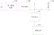
As shown in fig. 1, an embodiment of the present application provides a power adapter. The power adapter 10 includes a first rectifying circuit 110, a transforming circuit 120, a charging interface 170 and a tank circuit 130. The first rectifying circuit 110 is configured to rectify an alternating current AC input by a mains supply and output a first pulsating voltage. The input end of the voltage transformation circuit 120 is connected with the first rectification circuit 110, the output end of the voltage transformation circuit 120 is connected with the charging interface 170, and the energy storage circuit 130 is respectively connected with the output end of the voltage transformation circuit 120 and the charging interface 170. The voltage transformation circuit 120 is configured to receive the first ripple voltage output by the first rectification circuit 110, convert the first ripple voltage into a second ripple voltage, and output the second ripple voltage to the device to be charged 20 via the charging interface 170, so as to supply power to or charge the device to be charged 20. The energy storage circuit 130 can perform charging energy storage through the second ripple voltage output by the output terminal of the voltage transformation circuit 120, and discharge when the output voltage VOUT of the charging interface 170 is lower than a preset voltage threshold, so that the charging interface 170 outputs a constant dc voltage suitable for charging the device to be charged 20. Illustratively, the tank circuit 130 may include several farad capacitors or batteries connected in series. When the voltage transformation circuit is only used for realizing isolated transmission, the second ripple voltage can be the same as the first ripple voltage; when the voltage transformation circuit is further used for realizing voltage regulation, the voltage amplitude of the second pulsating voltage output after the first pulsating voltage is isolated and regulated by the voltage transformation circuit meets the charging or power supply requirement of the equipment to be charged, and when the voltage value of the second pulsating voltage is lower than a voltage threshold value, the voltage amplitude output through the charging interface finally meets the charging or power supply requirement of the equipment to be charged by matching with the energy storage circuit for discharging, so that the voltage continuously output by the charging interface of the power adapter is constant direct-current voltage meeting the requirement of the equipment to be charged.
Specifically, the first rectifying circuit 110 may implement rectification using a full bridge circuit to output a pulsating voltage. Optionally, the first rectifying circuit 110 may also implement rectification by using a half-bridge circuit.
It should be noted that the constant dc voltage in the embodiment of the present application refers to a dc voltage whose voltage fluctuation range is smaller than a certain range, and is different from a pulsating dc voltage, and can Charge or supply Power to a device 20 to be charged that does not support charging of the pulsating dc voltage, for example, the device 20 to be charged without a battery, the device 20 to be charged that adopts a Quick Charge (QC) protocol or a Power transfer (USB Power Delivery, USB PD) protocol, the device to be charged with a battery and the device to be charged that adopts a QC protocol or a USB PD protocol both require constant dc voltage for Power supply, have a high requirement for voltage ripples, and are difficult to normally supply Power when the voltage ripples are large, and if the device to be charged is supplied with a pulsating dc voltage, when the voltage value is lower than a voltage threshold, the conversion efficiency of the Power adapter may be reduced, or even the Power adapter may not continue to supply Power.
Compared with the power adapter in the conventional technology, the electrolytic capacitor is arranged on one side of the input end of the voltage transformation circuit for filtering so as to reduce the voltage fluctuation of the final output voltage, so that the scheme of charging or supplying constant direct-current voltage for the equipment to be charged 20 can be provided. The embodiment of the application cancels the setting of the electrolytic capacitor, and set up the energy storage circuit 130 on one side of the output end of the transformer circuit 120, make the energy storage circuit 130 capable of utilizing the second pulsating voltage output by the transformer circuit 120 to store energy, and discharge when the output voltage VOUT of the charging interface 170 is lower than the voltage threshold, with the second pulsating voltage combined action output by the transformer circuit 120, make the output voltage VOUT of the charging interface 170 be the constant direct current voltage suitable for charging or supplying power for the device 20 to be charged, effectively reduce the volume of the power adapter 10, and improve the volume of the power adapter 10. Compared with a power adapter which directly cancels an electrolytic capacitor to output pulsating voltage for power supply, the power adapter 10 in the embodiment of the present application can not only charge the device to be charged 20 which supports the pulsating voltage charging (since the device which supports the pulsating voltage charging also supports constant direct current voltage charging), but also supply power or charge the device to be charged 20 which does not have a battery and the device to be charged 20 which adopts a QC protocol or a USB PD protocol, and has higher compatibility.
In one embodiment, the energy storage circuit 130 charges when the output voltage VOUT of the charging interface 170 is higher than the voltage threshold, and at this time, the second ripple voltage output by the voltage transformation circuit 120 provides the output voltage VOUT for the charging interface 170, and also charges the energy storage circuit 130 to store energy, so that the energy storage circuit 130 can store energy in time, and it is ensured that the energy storage circuit 130 can discharge to provide energy for the output of the charging interface 170 when the output voltage VOUT of the charging interface 170 is lower than the voltage threshold.
As shown in fig. 2, in one embodiment, the energy storage circuit 130 includes a switching unit 131 and an energy storage element 132. The second pole of the energy storage element 132 is grounded, the first end of the switch unit 131 is connected to the charging interface 170, the second end of the switch unit 131 is connected to the first pole of the energy storage element 132, and the first pole of the energy storage element 132 is further connected to the charging interface 170. The switch unit 131 is configured to be turned on when the output voltage VOUT of the charging interface 170 is higher than a voltage threshold, so as to turn on a path between the energy storage element 132 and the output terminal of the transformer circuit 130, so that the energy storage element 132 can be charged by the second ripple voltage output by the transformer circuit 130. The switch unit 131 is turned off when the output voltage VOUT of the charging interface 170 is lower than the voltage threshold, and the energy storage element 132 discharges the output energy to the charging interface 170.
In particular, the energy storage element 132 may be a farad capacitor. The positive pole of the farad capacitor serves as the first pole of the energy storage element 132, and the negative pole of the farad capacitor serves as the second pole of the energy storage element 132.
Alternatively, the energy storage element 132 may be a battery. The positive pole of the battery serves as the first pole of the energy storage element 132 and the negative pole of the battery serves as the second pole of the energy storage element 132.
Because the withstand voltage value of the pull-up capacitor or the battery may be lower than the second ripple voltage output by the transformer circuit 120, the switch unit 131 may be connected to the energy storage element 132 and the output end of the transformer circuit 120 (i.e., the charging interface 170), so that the switching on control of the path between the energy storage element 132 and the output end of the transformer circuit 120 may be performed, the energy storage element may be charged and stored only when the output voltage of the charging interface is lower than the voltage threshold, the energy storage element may be stopped being charged after the output voltage of the charging interface reaches the voltage threshold, the charging time of the energy storage element may be controlled, and damage to the farad capacitor or the battery due to the overcharge exceeding the withstand voltage value may.
The battery used as the energy storage element 132 in this application is only used to provide short-time power supply when the second ripple voltage output by the transformer circuit 120 is not enough to meet the charging requirement of the device to be charged 20, and in order to avoid increasing the size of the power adapter, a battery with a smaller size and a smaller capacity may be used. Specifically, in order to ensure that the battery can discharge in time, the battery needs to have a high charging and discharging capability, for example, the charging and discharging capability at least needs to reach 7C or more.
The energy storage element 132 is discharged by a battery or a farad capacitor, and the conversion efficiency of the power adapter can be improved.
As shown in fig. 3, in one embodiment, the switching unit 131 includes a voltage regulator DW, a first switching tube Q1, and a first resistor R1. The first end of the first switch tube Q1 may be connected to the output ends of the charging interface 170 and the transforming circuit 120, the second end of the first switch tube Q1 is connected to the first pole of the energy storage element 132, the control end of the first switch tube Q1 is connected to the cathode of the voltage regulator tube DW, the anode of the voltage regulator tube DW is grounded, and the cathode of the voltage regulator tube DW is further connected to the first switch tube Q1 through the first resistor R1. The voltage regulator DW can stabilize the voltage at the control terminal of the first switch tube Q1 at a preset voltage threshold, and when the voltage at the first terminal of the first switch tube Q1 (i.e., the output voltage VOUT of the charging interface 170) is higher than the voltage threshold, the first switch tube Q1 is turned on, and at this time, the energy storage element 132 is charged. The first resistor R1 can limit the current flowing through the voltage regulator tube DW to prevent the voltage regulator tube DW from burning due to excessive heat consumption.
Specifically, the first switch Q1 may be an NMOS transistor as shown in fig. 3, or may be another switch, such as a PMOS transistor, a triode, or the like. When the first switch transistor Q1 is an NMOS transistor, the gate of the NMOS transistor serves as the control terminal of the first switch transistor Q1, the drain of the NMOS transistor serves as the first terminal of the first switch transistor Q1, and the source of the NMOS transistor serves as the second terminal of the first switch transistor Q1.
In one embodiment, the tank circuit 130 includes a plurality of farad capacitors C connected in series, as shown in figure 4. Because farad capacitor C withstand voltage value is lower, can improve energy storage circuit 130's withstand voltage value through a plurality of farad capacitors C of establishing ties, based on characteristics such as farad capacitor charge-discharge efficiency is high, need not to set up special charging circuit, can simply realize discharging when the output voltage of the interface that charges is less than the voltage threshold through the farad capacitor group of establishing ties to output and be applicable to the invariable direct current voltage who charges or supply power for waiting to charge equipment 20. In this embodiment, the voltage threshold is the voltage of the faraday capacitor series group, and when the output voltage of the charging interface is lower than the voltage of the faraday capacitor series group at the same time, the faraday capacitor series group discharges to the charging interface, and in the process, the voltage of the faraday capacitor series group gradually decreases until the discharge stops; and when the output voltage of the charging interface is higher than the voltage of the pull-down capacitor serial group at the same moment, the farad capacitor serial group receives the second pulsating voltage to perform charging energy storage, and the voltage of the farad capacitor serial group is gradually increased in the process until the voltage of the farad capacitor serial group at a certain moment is equal to the output voltage of the charging interface, namely, the charging is stopped. Namely, the charging or discharging of the farad capacitor series group is automatically triggered according to the voltage of the farad capacitor series group and the voltage of the second pulsating voltage. The quantity of the farad capacitors in the farad capacitor series group is determined according to the voltage amplitude of the second pulsating voltage, so that the withstand voltage value of the farad capacitor series group is not less than the voltage amplitude of the second pulsating voltage, and the farad capacitor series group is prevented from being broken down.
As shown in fig. 5, in one embodiment, the power adapter 10 further includes a boost circuit 140 and a control circuit 150. The boost circuit 140 is connected to the first electrode of the energy storage element 132 and the charging interface 170, and the control circuit 150 is connected to the boost circuit 140 and the charging interface 170. The voltage boost circuit 140 may boost the discharge voltage output by the energy storage element 132 according to the second control signal output by the control circuit 150; the control circuit 150 is configured to output a second control signal to control the boost circuit 140 according to the output voltage VOUT of the charging interface 170, so as to achieve dynamic balance of the output voltage, and even when the capacity of the energy storage element 132 is low, the voltage finally output to the device to be charged 20 by the charging interface 170 can also meet the voltage requirement of the device to be charged 20. Specifically, the control circuit 150 includes a control device having a control function, such as an MCU, a CPU, and an FPGA.
Referring to fig. 5, the boost circuit 140 includes a second switch Q2, an inductor L, a first diode D1, and a first capacitor C1. The first end of the second switch tube Q2 is connected to the first end of the energy storage element 132 through the inductor L, the second end of the second switch tube Q2 is grounded, the control end of the second switch tube Q2 is connected to the control circuit 150, the anode of the first diode D1 is connected to the first end of the second switch tube Q2, the cathode of the first diode D1 is connected to the charging interface 170, and the cathode of the first diode D1 is grounded through the first capacitor C1. The second switch tube Q2 receives the second control signal output by the control circuit 150 through the control end, and is turned on or off according to the indication of the second control signal, and the first diode D1 is used for ensuring the unidirectional conduction of the path between the inductor L and the charging interface 170; the first capacitor C1 is a filter capacitor.
When the second switching tube Q2 is turned on, the energy storage element 132 discharges to charge the inductor L, and the inductor L stores energy; when the second switch Q2 is turned off, the inductor L discharges to boost the voltage output by the energy storage element 132, and then outputs the discharge voltage to the charging interface 170.
Referring to fig. 8, in one embodiment, the boost circuit 140 further includes a third diode D3, and the third diode D3 is used to ensure the unidirectional output of the boost circuit 140.
As shown in fig. 6 to 8, in one embodiment, the transformer circuit 120 includes a transformer T, a second rectifying circuit 121, a modulating unit Q3 and a control circuit. The transformer T includes a primary winding and a secondary winding, the primary winding of the transformer T is an input end of the transformer circuit 120, a first end of the primary winding is connected to the first rectifying circuit 110, a second end of the primary winding is connected to a first end of the modulating unit Q3, a first end of the secondary winding is connected to the charging interface 170, a second end of the secondary winding is grounded to a second end of the modulating unit Q3 through the second rectifying circuit 121, and a control end of the modulating unit Q3 is configured to receive a first control signal. The transformer T is configured to convert the first pulsating voltage output by the first rectifying circuit 110 into a secondary voltage for output, and rectify the secondary voltage through the second rectifying circuit 121, so that the secondary winding outputs a second pulsating voltage to the charging interface 170. Specifically, the second rectifying circuit 121 may include a rectifying diode, an anode of the rectifying diode is grounded, and a cathode of the rectifying diode is connected to the second end of the secondary winding. The modulation unit Q3 is configured to modulate the first pulsating voltage according to a first control signal. The control circuit 150 is connected to the control end of the modulation unit Q3, and the control circuit 150 can also output a first control signal according to the output voltage VOUT of the charging interface 170 to control on/off of the modulation unit Q3, so as to modulate the first pulsating voltage.
Specifically, the modulation unit Q3 may employ an NMOS transistor as shown in fig. 5, or may employ other switching transistors, such as a PMOS transistor, a triode, and the like. When the modulation unit Q3 is an NMOS transistor, the gate of the NMOS transistor can be used as the control terminal of the modulation unit Q3, the drain of the NMOS transistor can be used as the first terminal of the modulation unit Q3, and the source of the NMOS transistor can be used as the second terminal of the modulation unit Q3.
Referring to fig. 5-8, in one embodiment, the power adapter 10 further includes a sampling circuit 160, and the sampling circuit 160 is configured to sample and feed back the output voltage VOUT of the charging interface 170 to the control circuit 150. Specifically, the sampling circuit 160 includes a second resistor R2 and a third resistor R3. A first end of the second resistor R2 is connected to the charging interface 170, and a second end of the second resistor R2 is connected to a first end of the third resistor R3 and the control circuit 150, respectively.
Referring to fig. 6, the control circuit 150 may output a first control signal to a control terminal of the modulation unit Q3 according to the output voltage VOUT collected by the sampling circuit 160, and control the modulation unit Q3 to modulate the first pulsating voltage; the control circuit 150 may further output a second control signal to the boost circuit according to the output voltage VOUT collected by the sampling circuit 160, so as to control the boost circuit to operate or shut down.
Referring to fig. 7, the control circuit 150 may output a first control signal to a control terminal of the modulation unit Q3 according to the output voltage VOUT collected by the sampling circuit 160, and control the modulation unit Q3 to modulate the first pulsating voltage.
Referring to fig. 7 and 8, in one embodiment, the power adapter 10 further includes an optocoupler 190 (i.e., an optocoupler) and a driver 180. The driver 180 is a switching tube driver and is connected with the control circuit 150 through the optocoupler 190, the driver 180 is further connected with a control end of the modulation unit Q3, the driver 180 is used for driving the modulation unit Q3 according to a first control signal output by the control circuit 150, and the modulation unit Q3 is arranged on the primary side of the transformer, is connected with the driver 180 and the control circuit 150 through the optocoupler 190, can realize the isolation of the primary side and the secondary side of the transformer T, and protects a circuit arranged on the secondary side of the transformer.
In one embodiment, the power adapter 10 further includes a second capacitor C2, and the second capacitor C2 is a filter capacitor for filtering the output voltage VOUT of the charging interface 170, and is a small MLCC capacitor, a ceramic capacitor or other small capacitor.
In one embodiment, the power adapter 10 further includes a filter circuit 101, and the filter circuit 101 is connected between the first rectifying circuit 110 and the primary winding of the transformer T for filtering the first pulsating voltage output by the first rectifying circuit 110. Specifically, the filter circuit 101 includes a third capacitor C3 and a fourth capacitor C4. The first end of the third capacitor C3 is connected to the first rectifying circuit, the second end of the third capacitor C3 is grounded, and the fourth capacitor C4 is connected in parallel to the third capacitor C3. It should be noted that the third capacitor C3 and the fourth capacitor C4 in this embodiment are small capacitors with small volume and small capacity, and an electrolytic capacitor is not required to convert the first pulsating voltage into a constant dc voltage, and specifically, an MLCC capacitor or a ceramic capacitor may be used.
In one embodiment, the power adapter 10 further includes a second diode D2, and the second diode D2 is used to ensure unidirectional output of the secondary winding of the transformer.
As shown in fig. 9, an embodiment of the present application further provides a power supply system, where the power supply system includes a device to be charged 20 and the power adapter 10 as described in the foregoing embodiment, and the charging interface 170 of the power adapter 10 is connected to the device to be charged 20 to charge the device to be charged 20. Based on the energy storage circuit 130 configured in the power adapter 10, when the output voltage VOUT of the charging interface 170 is lower than the voltage threshold, the power adapter 10 can provide a constant dc voltage to charge or supply power to the device to be charged 20, so that the size of the power adapter 10 is reduced, and the portability of the power adapter 10 is improved.
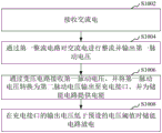
As shown in fig. 10, the present embodiment further provides a power supply method, which may be applied to the power adapter in the foregoing embodiment, where the power supply method includes steps 1002 to 1008.
Step 1002, receiving alternating current;
step 1004, rectifying the alternating current through a first rectifying circuit and outputting a first pulsating voltage;
step 1006, receiving the first ripple voltage through a voltage transformation circuit, converting the first ripple voltage into a second ripple voltage, outputting the second ripple voltage to a charging interface, and providing electric energy for the energy storage circuit;
in step 1008, the energy storage circuit discharges when the output voltage of the charging interface is lower than a preset voltage threshold value, so that the charging interface outputs a constant direct current voltage.
The power supply method will be described with reference to the power adapter 10 shown in fig. 1: the first rectifying circuit 110 receives alternating current, rectifies the input alternating current and outputs a first pulsating voltage, the voltage transformation circuit 120 receives the first pulsating voltage output by the first rectifying circuit 110, converts the first pulsating voltage into a second pulsating voltage and outputs the second pulsating voltage to the charging interface 170, and provides electric energy for the energy storage circuit 130, when the output voltage VOUT of the charging interface 170 is lower than a preset voltage threshold, the energy storage circuit 130 discharges electricity and interacts with the second pulsating voltage, and the charging interface 170 outputs a constant direct current voltage suitable for charging or supplying power to the device to be charged 20. In the power supply method in this embodiment, filtering by using an electrolytic capacitor is not required, and the purpose of outputting a constant dc voltage to charge or supply power to the device to be charged 20 can be achieved, so that the size of the power adapter 10 is effectively reduced, and the portability of the power adapter 10 is improved.
As shown in fig. 11, in one embodiment, the power supply method includes steps 1002-1008:
step 1002, receiving alternating current;
step 1004, rectifying the alternating current through a first rectifying circuit and outputting a first pulsating voltage;
step 1006, receiving the first ripple voltage through a voltage transformation circuit, converting the first ripple voltage into a second ripple voltage, outputting the second ripple voltage to a charging interface, and providing electric energy for the energy storage circuit;
step 1007, when the output voltage of the charging interface is higher than the voltage threshold, the energy storage circuit performs charging energy storage through the second pulsating voltage output by the voltage transformation circuit;
in step 1008, the energy storage circuit discharges when the output voltage of the charging interface is lower than a preset voltage threshold value, so that the charging interface outputs a constant direct current voltage.
As described with reference to the power adapter shown in fig. 1, the energy storage circuit 130 charges when the output voltage VOUT of the charging interface 170 is higher than the voltage threshold, and at this time, the second ripple voltage output by the voltage transformation circuit 120 provides the output voltage VOUT for the charging interface 170, and also charges the energy storage circuit 130 to store energy, so that the energy storage circuit 130 can store energy in time, and it is ensured that the energy storage circuit 130 can discharge energy to provide energy for the charging interface 170 when the output voltage VOUT of the charging interface 170 is lower than the voltage threshold.
As shown in fig. 12, in one embodiment, the power supply method includes steps 1002 to 1009:
step 1002, receiving alternating current;
step 1004, rectifying the alternating current through a first rectifying circuit and outputting a first pulsating voltage;
step 1006, receiving the first ripple voltage through a voltage transformation circuit, converting the first ripple voltage into a second ripple voltage, outputting the second ripple voltage to a charging interface, and providing electric energy for the energy storage circuit;
step 1007, when the output voltage of the charging interface is higher than the voltage threshold, the energy storage circuit performs charging energy storage through the second pulsating voltage output by the voltage transformation circuit;
step 1008, discharging the energy storage circuit when the output voltage of the charging interface is lower than a preset voltage threshold;
and step 1009, controlling the boosting circuit to boost the discharging voltage output by the energy storage circuit according to the output voltage of the charging interface.
As described with reference to the power adapter shown in fig. 3, for the energy storage circuit 130 with a low capacity or for realizing multi-voltage output, the voltage boost circuit 140 may be configured to boost the discharge voltage output by the energy storage circuit 130, and control the voltage boost circuit 140 according to the output voltage of the charging interface, so as to meet the voltage requirement of the device to be charged.
For the explanation of the power supply method, please refer to the above embodiment of the power adapter, which is not described herein again.
In the description herein, reference to the terms "exemplary," "particular," "in one embodiment," or the like, means that a particular feature, structure, material, or characteristic described in connection with the embodiment or example is included in at least one embodiment or example of the invention. In this specification, a schematic description of the above terminology may not necessarily refer to the same embodiment or example.
The technical features of the embodiments described above may be arbitrarily combined, and for the sake of brevity, all possible combinations of the technical features in the embodiments described above are not described, but should be considered as being within the scope of the present specification as long as there is no contradiction between the combinations of the technical features.
The above-mentioned embodiments only express several embodiments of the present invention, and the description thereof is more specific and detailed, but not construed as limiting the scope of the invention. It should be noted that, for a person skilled in the art, several variations and modifications can be made without departing from the inventive concept, which falls within the scope of the present invention. Therefore, the protection scope of the present patent shall be subject to the appended claims.
Claims (13)
1. A power adapter, comprising:
a first rectifying circuit for rectifying an input alternating current and outputting a first pulsating voltage;
the input end of the voltage transformation circuit is connected with the first rectifying circuit and is used for receiving the first pulsating voltage and converting the first pulsating voltage into a second pulsating voltage for output;
the charging interface is connected with the output end of the voltage transformation circuit;
the energy storage circuit is respectively connected with the output end of the voltage transformation circuit and the charging interface, and the energy storage circuit is used for discharging to the charging interface when the output voltage of the charging interface is lower than a preset voltage threshold value so that the charging interface outputs constant direct-current voltage.
2. The power adapter as claimed in claim 1, wherein the energy storage circuit is further configured to receive the second ripple voltage output by the transformer circuit for charging energy storage when the output voltage of the charging interface is higher than the voltage threshold.
3. The power adapter as described in claim 2, wherein said tank circuit comprises:
the first end of the switch unit is connected with the charging interface, and the switch unit is used for being switched on when the output voltage of the charging interface is higher than the voltage threshold;
and the energy storage element is connected with the second end of the switch unit and receives the second pulsating voltage to store charging energy when the switch unit is switched on.
4. The power adapter as described in claim 3, wherein said energy storage element is a farad capacitor or a battery.
5. The power adapter as claimed in claim 3, further comprising:
and the boosting circuit is respectively connected with the first electrode of the energy storage element and the charging interface, and is used for boosting the discharging voltage output by the energy storage element according to the output voltage of the charging interface and outputting the discharging voltage to the charging interface.
6. The power adapter as described in claim 1, wherein said tank circuit comprises: a series group of farad capacitors formed by a plurality of farad capacitors connected in series;
the farad capacitor series group is respectively connected with the output end of the voltage transformation circuit and the charging interface, and is used for discharging to the charging interface when the output voltage of the charging interface is lower than the voltage of the farad capacitor series group, and is also used for receiving a second pulsating voltage output by the voltage transformation circuit to charge and store energy when the output voltage of the charging interface is higher than the voltage of the farad capacitor series group.
7. The power adapter as claimed in any one of claims 1-6, wherein the transforming circuit comprises:
the transformer comprises a primary winding and a secondary winding, a first end of the primary winding is connected with the first rectifying circuit, a first end of the secondary winding is connected with the charging interface, and the transformer is used for converting the first pulsating voltage into a secondary voltage to be output;
the second rectifying circuit is connected with the second end of the secondary winding and used for rectifying the secondary voltage so as to enable the secondary winding to output the second pulsating voltage;
the modulation unit is connected between the second end of the primary winding and the ground and is used for modulating the first pulsating voltage;
and the control circuit is respectively connected with the charging interface and the control end of the modulation unit and is used for outputting a first control signal according to the output voltage of the charging interface so as to control the modulation unit to modulate the first pulsating voltage.
8. The power adapter as claimed in claim 7, wherein when the power adapter includes a voltage boost circuit, the control circuit is further configured to output a second control signal according to the output voltage of the charging interface, so as to control the voltage boost circuit to boost the discharging voltage output by the energy storage circuit and output the boosted discharging voltage to the charging interface.
9. The power adapter as claimed in claim 7, further comprising:
and the sampling circuit is respectively connected with the control circuit and the charging interface and is used for sampling the output voltage of the charging interface and feeding the output voltage back to the control circuit so as to enable the control circuit to identify the output voltage of the charging interface.
10. A power supply system, comprising:
a device to be charged;
the power adapter of any one of claims 1 to 9, wherein a charging interface of the power adapter is connected with the device to be charged so as to output a constant direct current voltage to the device to be charged.
11. A method of supplying power, comprising:
receiving alternating current;
rectifying the alternating current through a first rectifying circuit and outputting a first pulsating voltage;
receiving the first pulsating voltage through a voltage transformation circuit, converting the first pulsating voltage into a second pulsating voltage, outputting the second pulsating voltage to a charging interface, and providing electric energy for an energy storage circuit;
when the output voltage of the charging interface is lower than a preset voltage threshold value, the energy storage circuit discharges to the charging interface so that the charging interface outputs constant direct-current voltage.
12. The power supply method according to claim 11, characterized by further comprising:
when the output voltage of the charging interface is higher than the voltage threshold, the energy storage circuit performs charging energy storage through the second pulsating voltage output by the voltage transformation circuit.
13. The power supply method according to claim 11, characterized by further comprising:
and controlling the boosting circuit to boost the discharging voltage output by the energy storage circuit according to the output voltage of the charging interface and output the boosted discharging voltage to the charging interface.
Priority Applications (1)
| Application Number | Priority Date | Filing Date | Title |
|---|---|---|---|
| CN202110211952.8A CN112803794A (en) | 2021-02-25 | 2021-02-25 | Power adapter, power supply system and power supply method |
Applications Claiming Priority (1)
| Application Number | Priority Date | Filing Date | Title |
|---|---|---|---|
| CN202110211952.8A CN112803794A (en) | 2021-02-25 | 2021-02-25 | Power adapter, power supply system and power supply method |
Publications (1)
| Publication Number | Publication Date |
|---|---|
| CN112803794A true CN112803794A (en) | 2021-05-14 |
Family
ID=75815458
Family Applications (1)
| Application Number | Title | Priority Date | Filing Date |
|---|---|---|---|
| CN202110211952.8A Pending CN112803794A (en) | 2021-02-25 | 2021-02-25 | Power adapter, power supply system and power supply method |
Country Status (1)
| Country | Link |
|---|---|
| CN (1) | CN112803794A (en) |
Citations (17)
| Publication number | Priority date | Publication date | Assignee | Title |
|---|---|---|---|---|
| JPH07115704A (en) * | 1993-10-14 | 1995-05-02 | Toyota Motor Corp | Retarder |
| CN2558185Y (en) * | 2002-06-14 | 2003-06-25 | 中诠光电股份有限公司 | Fluorescent lamp set |
| JP2004350440A (en) * | 2003-05-23 | 2004-12-09 | Mitsuba Corp | Power supply circuit of automobile |
| EP2684732A1 (en) * | 2012-07-09 | 2014-01-15 | ABB Oy | Electrical system having a DC link |
| CN203722258U (en) * | 2013-11-04 | 2014-07-16 | 无锡新畅电子有限公司 | Equalization control panel of battery pack |
| CN104283409A (en) * | 2012-11-05 | 2015-01-14 | 矽力杰半导体技术(杭州)有限公司 | Self-powered source electrode drive circuit and switch power source with self-powered source electrode drive circuit |
| CN104600967A (en) * | 2015-01-07 | 2015-05-06 | 北京天诚同创电气有限公司 | high-voltage direct-current power supply circuit |
| CN204651941U (en) * | 2015-05-25 | 2015-09-16 | 镇江市高等专科学校 | Intelligent micro-grid special inverter |
| CN205610314U (en) * | 2016-05-13 | 2016-09-28 | 长沙威胜信息技术有限公司 | Super capacitor charging and discharging circuit and metering device who makes with this circuit |
| CN205882806U (en) * | 2016-02-05 | 2017-01-11 | 广东欧珀移动通信有限公司 | A charging system and power adapter for terminal |
| CN109143090A (en) * | 2018-08-14 | 2019-01-04 | Oppo广东移动通信有限公司 | Apparatus control method, device, storage medium and electronic equipment |
| CN208489657U (en) * | 2016-01-15 | 2019-02-12 | 诺瓦斯株式会社 | The battery shape power supply device for having wireless communication function |
| CN109494823A (en) * | 2017-09-12 | 2019-03-19 | 屹立电动技术有限公司 | Household energy storage battery system |
| CN111193317A (en) * | 2020-01-22 | 2020-05-22 | 福建工程学院 | Power-down protection circuit for terminal equipment |
| CN112234848A (en) * | 2020-09-30 | 2021-01-15 | Oppo广东移动通信有限公司 | Power supply device, charging method and system, and computer-readable storage medium |
| CN112234849A (en) * | 2020-09-30 | 2021-01-15 | Oppo广东移动通信有限公司 | Power supply device and charging method |
| CN112350567A (en) * | 2020-11-12 | 2021-02-09 | Oppo广东移动通信有限公司 | Power supply, power supply providing method and computer storage medium |
-
2021
- 2021-02-25 CN CN202110211952.8A patent/CN112803794A/en active Pending
Patent Citations (18)
| Publication number | Priority date | Publication date | Assignee | Title |
|---|---|---|---|---|
| JPH07115704A (en) * | 1993-10-14 | 1995-05-02 | Toyota Motor Corp | Retarder |
| CN2558185Y (en) * | 2002-06-14 | 2003-06-25 | 中诠光电股份有限公司 | Fluorescent lamp set |
| JP2004350440A (en) * | 2003-05-23 | 2004-12-09 | Mitsuba Corp | Power supply circuit of automobile |
| EP2684732A1 (en) * | 2012-07-09 | 2014-01-15 | ABB Oy | Electrical system having a DC link |
| CN104283409A (en) * | 2012-11-05 | 2015-01-14 | 矽力杰半导体技术(杭州)有限公司 | Self-powered source electrode drive circuit and switch power source with self-powered source electrode drive circuit |
| CN203722258U (en) * | 2013-11-04 | 2014-07-16 | 无锡新畅电子有限公司 | Equalization control panel of battery pack |
| CN104600967A (en) * | 2015-01-07 | 2015-05-06 | 北京天诚同创电气有限公司 | high-voltage direct-current power supply circuit |
| CN204651941U (en) * | 2015-05-25 | 2015-09-16 | 镇江市高等专科学校 | Intelligent micro-grid special inverter |
| CN208489657U (en) * | 2016-01-15 | 2019-02-12 | 诺瓦斯株式会社 | The battery shape power supply device for having wireless communication function |
| CN205882806U (en) * | 2016-02-05 | 2017-01-11 | 广东欧珀移动通信有限公司 | A charging system and power adapter for terminal |
| JP2018512030A (en) * | 2016-02-05 | 2018-04-26 | グァンドン オッポ モバイル テレコミュニケーションズ コーポレーション リミテッド | Charging method, adapter and mobile terminal |
| CN205610314U (en) * | 2016-05-13 | 2016-09-28 | 长沙威胜信息技术有限公司 | Super capacitor charging and discharging circuit and metering device who makes with this circuit |
| CN109494823A (en) * | 2017-09-12 | 2019-03-19 | 屹立电动技术有限公司 | Household energy storage battery system |
| CN109143090A (en) * | 2018-08-14 | 2019-01-04 | Oppo广东移动通信有限公司 | Apparatus control method, device, storage medium and electronic equipment |
| CN111193317A (en) * | 2020-01-22 | 2020-05-22 | 福建工程学院 | Power-down protection circuit for terminal equipment |
| CN112234848A (en) * | 2020-09-30 | 2021-01-15 | Oppo广东移动通信有限公司 | Power supply device, charging method and system, and computer-readable storage medium |
| CN112234849A (en) * | 2020-09-30 | 2021-01-15 | Oppo广东移动通信有限公司 | Power supply device and charging method |
| CN112350567A (en) * | 2020-11-12 | 2021-02-09 | Oppo广东移动通信有限公司 | Power supply, power supply providing method and computer storage medium |
Similar Documents
| Publication | Publication Date | Title |
|---|---|---|
| JP6623237B2 (en) | Adapter and charge control method | |
| CN107836067B (en) | Adapter and charging control method | |
| US7017055B1 (en) | Hub that can supply power actively | |
| CN100461582C (en) | Battery pack | |
| JP2019195266A (en) | Apparatus to be charged and charging method | |
| WO2016013451A1 (en) | Charging circuit, electronic device using same, and charger | |
| TWI636358B (en) | Adapter and charging control method | |
| CN109904913B (en) | Charging equipment and quick charging circuit thereof | |
| CN111900780A (en) | Mobile power supply quick charging protocol conversion device and control method thereof | |
| US8384356B2 (en) | Self contained power source | |
| CN102882417A (en) | Uninterrupted power supply (UPS) isolation type bidirectional direct-current converter | |
| US20110254510A1 (en) | Intermittently outputted power supply system | |
| CN112803794A (en) | Power adapter, power supply system and power supply method | |
| CN214154112U (en) | Two-in-one power supply | |
| US10056831B2 (en) | Filter and method for direct rectification grid-powered power supplies | |
| CN109639118B (en) | Self-powered circuit of switching power supply, control chip, switching power supply and electric device | |
| KR20220028119A (en) | Power storage devices, control devices, and power storage systems | |
| CN107846143B (en) | Capacitive power conversion circuit and charging control method | |
| CN111917147A (en) | Charging circuit and charging control method | |
| CN211127261U (en) | Portable power supply device for multifunctional output and quick charging of charger and mobile power supply | |
| CN220732395U (en) | Energy storage power supply device | |
| CN217904071U (en) | Charging circuit and charger | |
| CN215580523U (en) | Medical equipment and power supply management system thereof | |
| CN210297548U (en) | Lithium battery pack compatible with PD charger | |
| CN213402843U (en) | Intelligent power adapter |
Legal Events
| Date | Code | Title | Description |
|---|---|---|---|
| PB01 | Publication | ||
| PB01 | Publication | ||
| SE01 | Entry into force of request for substantive examination | ||
| SE01 | Entry into force of request for substantive examination | ||
| RJ01 | Rejection of invention patent application after publication | ||
| RJ01 | Rejection of invention patent application after publication |
Application publication date: 20210514 |