CN112166312B - Sensor device and method of operating a sensor device - Google Patents
Sensor device and method of operating a sensor device Download PDFInfo
- Publication number
- CN112166312B CN112166312B CN201980035474.0A CN201980035474A CN112166312B CN 112166312 B CN112166312 B CN 112166312B CN 201980035474 A CN201980035474 A CN 201980035474A CN 112166312 B CN112166312 B CN 112166312B
- Authority
- CN
- China
- Prior art keywords
- circuit
- sensor
- test
- pressure sensor
- digital
- Prior art date
- Legal status (The legal status is an assumption and is not a legal conclusion. Google has not performed a legal analysis and makes no representation as to the accuracy of the status listed.)
- Active
Links
Images


Classifications
-
- G—PHYSICS
- G01—MEASURING; TESTING
- G01L—MEASURING FORCE, STRESS, TORQUE, WORK, MECHANICAL POWER, MECHANICAL EFFICIENCY, OR FLUID PRESSURE
- G01L27/00—Testing or calibrating of apparatus for measuring fluid pressure
- G01L27/002—Calibrating, i.e. establishing true relation between transducer output value and value to be measured, zeroing, linearising or span error determination
-
- G—PHYSICS
- G01—MEASURING; TESTING
- G01L—MEASURING FORCE, STRESS, TORQUE, WORK, MECHANICAL POWER, MECHANICAL EFFICIENCY, OR FLUID PRESSURE
- G01L9/00—Measuring steady of quasi-steady pressure of fluid or fluent solid material by electric or magnetic pressure-sensitive elements; Transmitting or indicating the displacement of mechanical pressure-sensitive elements, used to measure the steady or quasi-steady pressure of a fluid or fluent solid material, by electric or magnetic means
- G01L9/0041—Transmitting or indicating the displacement of flexible diaphragms
- G01L9/0072—Transmitting or indicating the displacement of flexible diaphragms using variations in capacitance
-
- G—PHYSICS
- G01—MEASURING; TESTING
- G01D—MEASURING NOT SPECIALLY ADAPTED FOR A SPECIFIC VARIABLE; ARRANGEMENTS FOR MEASURING TWO OR MORE VARIABLES NOT COVERED IN A SINGLE OTHER SUBCLASS; TARIFF METERING APPARATUS; MEASURING OR TESTING NOT OTHERWISE PROVIDED FOR
- G01D5/00—Mechanical means for transferring the output of a sensing member; Means for converting the output of a sensing member to another variable where the form or nature of the sensing member does not constrain the means for converting; Transducers not specially adapted for a specific variable
- G01D5/12—Mechanical means for transferring the output of a sensing member; Means for converting the output of a sensing member to another variable where the form or nature of the sensing member does not constrain the means for converting; Transducers not specially adapted for a specific variable using electric or magnetic means
- G01D5/14—Mechanical means for transferring the output of a sensing member; Means for converting the output of a sensing member to another variable where the form or nature of the sensing member does not constrain the means for converting; Transducers not specially adapted for a specific variable using electric or magnetic means influencing the magnitude of a current or voltage
- G01D5/24—Mechanical means for transferring the output of a sensing member; Means for converting the output of a sensing member to another variable where the form or nature of the sensing member does not constrain the means for converting; Transducers not specially adapted for a specific variable using electric or magnetic means influencing the magnitude of a current or voltage by varying capacitance
-
- G—PHYSICS
- G01—MEASURING; TESTING
- G01L—MEASURING FORCE, STRESS, TORQUE, WORK, MECHANICAL POWER, MECHANICAL EFFICIENCY, OR FLUID PRESSURE
- G01L27/00—Testing or calibrating of apparatus for measuring fluid pressure
- G01L27/002—Calibrating, i.e. establishing true relation between transducer output value and value to be measured, zeroing, linearising or span error determination
- G01L27/005—Apparatus for calibrating pressure sensors
-
- G—PHYSICS
- G01—MEASURING; TESTING
- G01L—MEASURING FORCE, STRESS, TORQUE, WORK, MECHANICAL POWER, MECHANICAL EFFICIENCY, OR FLUID PRESSURE
- G01L27/00—Testing or calibrating of apparatus for measuring fluid pressure
- G01L27/007—Malfunction diagnosis, i.e. diagnosing a sensor defect
Landscapes
- Physics & Mathematics (AREA)
- General Physics & Mathematics (AREA)
- Chemical & Material Sciences (AREA)
- Analytical Chemistry (AREA)
- Health & Medical Sciences (AREA)
- Engineering & Computer Science (AREA)
- Biomedical Technology (AREA)
- Measuring Fluid Pressure (AREA)
Abstract
一种传感器装置(10),包括:压力传感器(12)、电容至数字转换器(13)、测试电路(14)以及开关电路(15),该压力传感器被实现为电容式压力传感器,该开关电路将电容至数字转换器(13)和测试电路(14)耦接至压力传感器(12)。
A sensor device (10) comprising a pressure sensor (12), a capacitance-to-digital converter (13), a test circuit (14) and a switch circuit (15), the pressure sensor being implemented as a capacitive pressure sensor, the switch A circuit couples a capacitance-to-digital converter (13) and a test circuit (14) to the pressure sensor (12).
Description
The present disclosure relates to a sensor device and a method of operating a sensor device.
The sensor means comprise a sensor, for example a pressure sensor. Pressure sensors typically have a membrane. The membrane may be fabricated as a microelectromechanical systems membrane, abbreviated as MEMS membrane. The membrane is deflected in the presence of a pressure difference between the two sides of the membrane. The pressure sensor is typically implemented as a capacitive pressure sensor. Thus, the deflection of the membrane results in a change of the capacitance value of the pressure sensor. Therefore, the pressure sensor is typically connected to a capacitance-to-digital converter to generate a digital value that depends on the pressure difference between the two sides of the membrane. The stability and sensitivity of pressure measurements is highly dependent on the physical properties of the membrane. These physical characteristics may be different in different examples of pressure sensors and may change over the life of the pressure sensor.
It is an object to provide a sensor device and a method of operating the sensor device which improve the accuracy of the sensor measurements.
These objects are achieved by the subject matter of the independent claims. Further developments and embodiments are described in the dependent claims.
The above definitions apply also to the following description, unless otherwise indicated.
In an embodiment, a sensor device includes a pressure sensor, a capacitance-to-digital converter, a test circuit, and a switching circuit coupling the capacitance-to-digital converter and the test circuit to the pressure sensor. The pressure sensor is implemented as a capacitive pressure sensor.
Advantageously, the measurement of the capacitive pressure sensor can be performed by a capacitance-to-digital converter. The test circuit is designed to obtain further information about the pressure sensor, for example calibration data. Thus, the digital signal provided by the capacitance-to-digital converter can be corrected using the further information.
In an embodiment, the sensor device comprises a semiconductor body. The semiconductor body includes at least a pressure sensor, a capacitance-to-digital converter, a test circuit, and a switching circuit. The pressure sensor, the capacitance-to-digital converter, the test circuit and the switching circuit are integrated on a first surface of the semiconductor body. The sensor device comprises only a single semiconductor body.
In an alternative embodiment, the sensor device comprises a semiconductor body and a further semiconductor body, which together comprise a pressure sensor, a capacitance-to-digital converter, a test circuit and a switching circuit.
In an embodiment, the sensor device includes a digital circuit coupled to the capacitance-to-digital converter, the test circuit, and the switching circuit. The semiconductor body may include digital circuitry.
In an embodiment, the sensor device comprises a memory connected to the digital circuit. The semiconductor body may include a memory.
In an embodiment, in a test phase of operation, the digital circuit controls the switching circuit such that the test circuit is coupled to the pressure sensor, or such that the test circuit and the capacitance-to-digital converter are coupled to the pressure sensor.
In an embodiment, in a test phase of operation, the digital circuit controls the switching circuit such that the test circuit is coupled exclusively or only to the pressure sensor, wherein the capacitance-to-digital converter is not coupled to the pressure sensor. Alternatively, during a test phase of operation, the digital circuit controls the switching circuit such that both the test circuit and the capacitance-to-digital converter are coupled to the pressure sensor.
During a test phase of operation, the digital circuit may store the correction data in the memory.
In an embodiment, during a measurement phase of operation, the digital circuit controls the switching circuit such that the capacitance-to-digital converter is coupled to the pressure sensor.
During the measurement phase of operation, the digital circuitry may provide a digitized pressure signal based on the digital signal provided by the capacitance-to-digital converter and the calibration data stored in the memory.
In an embodiment, in a test phase of operation, the sensor device performs a frequency sweep and determines a resonant frequency of a membrane of the pressure sensor. Alternatively, the sensor device determines the figure of merit. The quality factor may be equal to the width of the resonance peak.
In an embodiment, the test circuit performs a frequency sweep and generates a test result signal. The digital circuit determines the resonant frequency and optionally also the quality factor from the test result signal. The digital circuit determines correction data from the resonant frequency and optionally also from the quality factor.
In an embodiment, the pressure sensor comprises a first electrode and a second electrode. The test circuit includes a first terminal and a second terminal. The switching circuit couples a first terminal of the test circuit to the first electrode and a second terminal of the test circuit to the second electrode.
In an embodiment, the switching circuit couples a first input of the capacitance-to-digital converter to the first electrode and a second input of the capacitance-to-digital converter to the second electrode.
In an embodiment, the test circuit comprises a current source having a first terminal connected to the first terminal of the test circuit and a second terminal connected to the second terminal of the test circuit.
In an embodiment, the test circuit comprises a timing generator connected to the current source and providing the modulator clock signal to the current source. A current source controlled by a timing generator may operate, for example, a modulator.
In an embodiment, the test circuit comprises a demodulator circuit having a first input connected to the first terminal of the test circuit and a second input connected to the second terminal of the test circuit.
In an embodiment, the timing generator is connected to the demodulator circuit and provides a demodulator clock signal to the demodulator circuit.
In an embodiment, the test circuit comprises a filter connected to the output side of the demodulator circuit. The test circuit includes an analog-to-digital converter connected to the output side of the filter and to the input of the digital circuit.
In an embodiment, the test circuit includes a bias circuit having a first terminal connected to the first terminal of the test circuit and a second terminal connected to the second terminal of the test circuit. The bias circuit may be configured to adjust a DC bias voltage of the first electrode and a DC bias voltage of the second electrode.
In an embodiment, the bias circuit provides a source voltage to the first and second terminals of the bias circuit during a test phase of operation. Thus, the first electrode and the second electrode of the pressure sensor are set at the same DC potential by the bias circuit.
In an alternative embodiment, the bias circuit applies a source voltage between the first and second terminals of the bias circuit during a test phase of operation. Thus, the first and second electrodes of the pressure sensor may have different DC potentials. The difference between the two DC potentials is equal to the source voltage. The capacitance-to-digital converter generates a digital signal according to a capacitance value of the pressure sensor. The capacitance value is a function of the value of the source voltage. The digital circuit uses the digital signal to determine correction data.
In a further development, the bias circuit generates at least two different values of the source voltage. The capacitance-to-digital converter generates at least two values of the digital signal. The digital circuit determines correction data from at least two values of the digital signal.
In an embodiment, the sensor device comprises a further pressure sensor. The further pressure sensor may be implemented as a further capacitive pressure sensor.
In an embodiment, a switching circuit couples the capacitance-to-digital converter and the test circuit to another pressure sensor.
In an embodiment, a method of operating a sensor device comprises:
in a measurement phase of operation, coupling a capacitance-to-digital converter to the pressure sensor via a switching circuit, and
in a test phase of operation, the test circuit is coupled to the pressure sensor via the switching circuit, or the test circuit and the capacitance-to-digital converter are coupled to the pressure sensor.
The pressure sensor is implemented as a capacitive pressure sensor.
In an embodiment, in another measurement phase of operation, the capacitance-to-digital converter is coupled to another pressure sensor via a switching circuit.
In an embodiment, in a further test phase of operation, the test circuit is coupled to a further pressure sensor via the switching circuit. Alternatively, in another test phase of operation, the test circuit and the capacitance-to-digital converter are coupled to another pressure sensor via a switching circuit.
In an embodiment, during a measurement phase of operation, the digital circuit provides a digitized pressure signal as a function of the digital signal provided by the capacitance-to-digital converter and the calibration data stored in the memory.
In an embodiment, in a test phase of operation, the digital circuit stores the correction data in the memory according to at least one of a test result signal provided by the test circuit and a digital signal provided by the capacitance-to-digital converter.
The method of operating a sensor device may for example be realized by a sensor device according to one of the embodiments defined above. The method of operating the sensor device may be implemented as a method for pressure measurement or operating a pressure sensor.
The measurement phase may follow the test phase.
Alternatively, the test phase may follow a previous measurement phase, with the measurement phase following the test phase. Thus, the test phase may be between two measurement phases.
In an embodiment, the sensor device comprises a sensor instead of a pressure sensor. The sensor may be, for example, a micro-electromechanical system sensor (abbreviated as MEMS sensor), a capacitive sensor, a physical sensor, or a mechanical sensor.
In an embodiment, the sensor device comprises an accelerometer or a gyroscope instead of a pressure sensor. Capacitance-voltage measurement or method and/or resonance frequency measurement or method for a device that can be electrostatically actuated. Such a device can use the methods and circuits described in this disclosure if, for example, an AC/DC bias voltage can be applied to an electrode embedded in a movable structure and a counter electrode in a fixed structure in the device.
In an embodiment, the sensor device (abbreviated device) is configured to measure a resonance frequency of a membrane of the pressure sensor. The apparatus is configured for in-situ calibration of a pressure sensor. The sensor device may be implemented on top of an application specific integrated circuit, ASIC for short. The sensor device is integrated with the ASIC to reduce cross talk and reduce footprint and package height.
In an embodiment, the pressure sensor can have a high absolute accuracy of 0.5mbar at 1000mbar after calibration. This equates to a relative accuracy of 0.05%. This is a very low value for mechanical devices. This means that small changes in material properties, external forces, etc. can cause significant shifts in sensor output readings, e.g., digital signals. Therefore, it is desirable to calibrate possible accuracy offsets in the field during the lifetime of the pressure sensor. In this disclosure, two methods are described that can be used together or only one of them: the resonant frequency method and the capacitance-voltage method, which is also referred to as the CV method. The capacitance-voltage method may also be referred to as a capacitance-to-voltage bias method, a capacitance-to-voltage bias method, or a capacitance-to-DC bias method, which is abbreviated as a CV method. C-V represents capacitance-voltage: that is, the capacitance is a function of the applied bias voltage. In the latter approach, a bias voltage is applied across the electrodes such that the flexible top electrode is electrostatically attracted toward the fixed bottom electrode. Due to electrostatic attraction, the capacitance may increase parabolically with the bias voltage. The bias voltage is a DC bias voltage. The bias voltage may be implemented as a source voltage. In both methods, the device performs dedicated measurements, called compensation measurements, from time to sense changes in the pressure sensor transducer. These variations are responsible for the sensor output offset. By detecting these changing characteristics, the device is able to compensate for them and reduce the output offset.
In an embodiment, the pressure sensor is plugged into the mobile device and calibrated in the field. The pressure sensor is designed such that the sensor output offset is low. With the proposed method, the residual output offset can be calibrated or reduced such that the pressure sensor has a constant high absolute accuracy over the lifetime. The sensor output shifts due to small changes in the transducer and/or package characteristics. The transducer is a freely suspended membrane on top of the sealed chamber. The chamber pressure is usually very small, in the order of a few mbar, abbreviated to mbar. The external atmospheric pressure presses on the membrane, causing it to bend downwards in the direction of the bottom electrode on the other side of the cavity. Inside the membrane is a top electrode, and the capacitance between the top electrode and the bottom electrode is measured. The capacitance is directly related to the atmospheric pressure. The properties of the membrane determine to a large extent the properties of the pressure sensor.
The sensor output offset is mainly caused by changes in the membrane properties. By measuring changes in the film properties, for example by in situ compensation measurements using a sensor device, the sensor output offset caused by such changes can be compensated for. Typically, a conventional specification for such drift is in the order of + -1 mbar sensor drift per year. Thus, after a lifetime of, for example, 10 years, the drift reaches ± 10mbar (═ 1%). Typical weld drift for conventional equipment is also on the order of + -1 mbar sensor drift. Advantageously, the sensor device and the method for operating the sensor device may compensate for all these drift effects to keep the accuracy within ± 1mbar accuracy during lifetime. Note that the sensor drift that needs to be corrected is small, which justifies limiting the drift compensation to first order effects.
The most important membrane properties are described by the effective membrane stiffness. The effective membrane stiffness is determined by sensor characteristics such as the materials in the membrane layer stack, the lateral size of the membrane, the effective membrane stress and the cavity pressure. Sensor drift is mainly caused by changes in the effective membrane stiffness. The sensor arrangement detects changes in effective membrane stiffness so that sensor drift can be compensated for in situ.
The following possible changes in sensor characteristics affect the effective membrane stiffness: changes in cavity pressure may be due to outgassing of surrounding layers or by in-diffusion through the membrane. This may be a change in effective stress due to stress relaxation in the membrane or anchor (anchor) or stress changes in the CMOS back-end aluminum.
Such devices may not be able to compensate for, for example, catastrophic failures such as film breakage or drift in the analog front end of the ASIC.
The present disclosure relates to pressure sensors using MEMS membranes; the film can be modeled as a capacitor plus a series of parasitic elements in parallel. The AC response is measured by applying an alternating bias voltage across the top and bottom electrodes. The membrane can be made to resonate when an alternating bias voltage is applied across the top and bottom electrodes at a particular characteristic frequency, i.e., the resonant frequency. The AC response shows a peak in resonance whose value is related to some physical property of the membrane and the underlying cavity. The resonant frequency is the resonance of the film properties and the cavity properties. Measuring the resonant frequency of the membrane gives information about the membrane stiffness, the cavity pressure and the pressure sensitivity. Being able to resonate the membrane enables detection of defects and determination of whether the membrane is properly released. The information obtained from the resonance frequency measurement enables the determination of the total transducer yield.
The on-chip resonant measurement circuit enables a determination of whether an unacceptable change in film stress and/or wafer bow has occurred. If the membrane is not sealed or outgassing occurs in the cavity, it is useful to determine the resonant frequency and the width of the resonant peak (i.e., the full width at half maximum, FWHM for short). Based on this information, a figure of merit can be determined. The device enables frequency scanning to be performed in a large frequency range of 1kHz … … 100kHz in the vicinity of the natural resonance frequency (700kHz to 900kHz) of the pressure-sensitive film.
Measuring the resonance frequency of the pressure sensor membrane gives information about the stiffness of the membrane and the presence of defects. For example, if there is no resonant frequency, the membrane is not properly released or even broken. If the resonance frequency is significantly higher, the membrane can (partially) adhere. If there are particles or etching residues remaining in the cavity, the resonance frequency will be significantly different from the neighboring devices, i.e. the resonance frequency is typically larger due to the larger mass/stiffness of the membrane. If the membrane is leaky/unsealed, the resonance frequency also increases and can therefore be used to detect faulty devices. The resonant frequency is directly related to the mass and stress in the pressure sensitive membrane. The on-chip integrated resonant measurement circuit can be utilized to accurately monitor changes in film stress over time. The film stress can vary for several reasons: 1) variations in (wafer) bowing due to stress variations in Plasma Enhanced Chemical Vapor Deposition (PECVD) deposited silicon oxide and/or silicon nitride layers used in back-end-of-the-line (BEOL) interconnects, 2) variations in the intrinsic stress and/or possibly also the elastic modulus of the aluminum interconnect layer due to large temperature excursions: aluminum is known to exhibit viscoelastic and even viscoplastic behavior that affects wafer bending and thus also film stress, 3) viscoelastic damping by air outside the chamber and/or viscoelastic damping by gases trapped inside the chamber: the viscosity of the gas molecules causes energy to be dissipated by compression and shear, the resonant frequency increases due to the buffer effect if gas is present in the cavity, 4) the change in film stack stress, e.g., the compressive stress of the PECVD silicon nitride seal can change due to structural rearrangement of the material over time.
The width of the resonance peak enables the quality factor of the resonator to be determined. The figure of merit is a measure of the damping behavior. A low quality factor indicates that membrane movement is inhibited during oscillation, for example due to the presence of air or gas trapped within the cavity. The inverse of the figure of merit is proportional to the cavity pressure. Outgassing of the cavity (caused by gases escaping from the cavity and gas molecules diffusing into the cavity) causes the sensor to drift. The device is designed to determine the width of the resonant frequency peak.
In an embodiment, the sensor device comprises a capacitance-to-digital converter circuit having four terminals and two pressure sensors. Both pressure sensors have a pressure sensitive membrane. In a test phase of operation, the membranes of two pressure sensors connected in parallel may be tested by the sensor device. If two pressure membranes are connected in parallel to the resonant excitation circuit, two resonance peaks will occur, which will partially overlap depending on the respective stress state of the two membranes. The device performs a frequency sweep and enables the peak positions of two resonant frequency peaks to be distinguished. Due to the damping, the resonance frequencies will partly overlap. Without frequency scanning, the determination of the full width at half maximum may produce erroneous results. The device is designed to determine multiple resonant frequencies using multiple capacitive pressure sensor membranes.
In an embodiment, the test circuit is connected to exactly one pressure sensor. The pressure sensor comprises exactly one membrane. Thus, one single membrane is connected to the resonant frequency circuit. Even if multiple films are used for the capacitance-to-digital converter, the test circuit is connected to one single film.
The test circuit may be coupled to exactly one pressure sensor via the switching circuit. The pressure sensor comprises exactly one membrane. In the test phase of operation, exactly one membrane is tested by the sensor device. The exactly one membrane is tested separately in the testing phase.
Advantageously, performing a frequency sweep more easily oscillates the membrane. If the resonant frequency is known in advance, the membrane can be oscillated using a simple oscillator circuit. In the case where a large shift occurs or the quality factor is low, it becomes difficult to excite the membrane if the membrane is not excited at an accurate frequency. However, when the results are analyzed over the entire frequency, a quality factor can be obtained in addition to the resonance frequency. With this apparatus, the yield can be optimized by measuring the film characteristics at the time of wafer sorting. The apparatus enables defects in the film to be verified at wafer sorting before the product is assembled and calibrated. In the case of products sold as good known dies, fault coverage can be significantly increased. The sensor device is configured to recalibrate the apparatus in-situ taking into account the increments of the resonant frequency and the quality factor.
Calibration of the pressure sensor is added between the frequency method and the CV method. Advantageously, an accurate pressure reference, such as a second pressure sensor, may not be required. Thus, drift correction can be done in the field. The pressure sensor remains relatively accurate. The calibration method does not require internet access or GPS data. The method will therefore also work in devices without such functionality. Here, the already existing bottom and top electrodes are used to apply additional force. The resonant frequency enables monitoring of stress changes as well as cavity pressure changes. The method improves the accuracy of the device in the field and compensates for small drifts. Additional external input may not be required.
The sensor device is implemented as a circuit that applies a stimulus at a particular frequency and then synchronously demodulates the response to extract the in-phase and quadrature components at that frequency. The sensor device may be implemented as an embedded integrated circuit that performs a frequency sweep that results in a resonant frequency response of the plurality of membranes and a width of the resonant frequency peak. The apparatus is implemented as a circuit capable of determining a resonant frequency of a capacitive pressure sensor membrane using a frequency sweep of a clock signal in both 0 ° and 90 ° modes of operation.
The following description of the figures of the embodiments may also illustrate and explain aspects of the sensor device and a method of operating the sensor device. Devices and circuit parts having the same structure and the same effects are denoted by the same reference numerals, respectively. In the case where the devices or circuit components in different drawings correspond to each other in their functions, the description thereof will not be repeated for each of the following drawings.
Fig. 1A to 1C show examples of embodiments of a sensor device;
FIG. 2 shows an example of a pressure sensor;
fig. 3A to 3E show another example of an embodiment of a sensor device;
fig. 4 shows an example of signals of a sensor device;
fig. 5A and 5B show examples of simulation results of the sensor device;
FIGS. 6A and 6B illustrate examples of models and measurements of a pressure sensor;
fig. 7A and 7B show examples of measurement results of the pressure sensor; and
fig. 8 shows a further example of an embodiment of the sensor device.
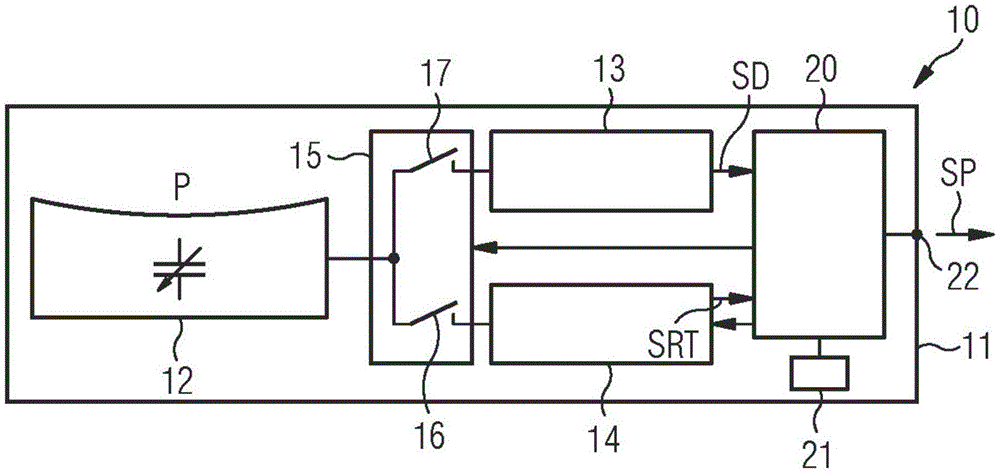
Fig. 1A shows an example of an embodiment of a sensor device 10. The sensor device 10 (simply referred to as device) is realized on a semiconductor body 11. The sensor device 10 comprises a pressure sensor 12 realized as a capacitive pressure sensor 12 and simply referred to as sensor. Thus, the sensor device 10 is realized as a pressure sensor device. Further, the apparatus 10 comprises a capacitance-to-digital converter 13, a test circuit 14 and a switching circuit 15. The capacitance-to-digital converter 13 can be simply referred to as a converter. The converter 13 is coupled to the sensor 12 via a switching circuit 15. The test circuit 14 is coupled to the sensor 12 via a switching circuit 15.
The switching circuit 15 includes a first switch 16. A first switch 16 couples the test circuit 14 to the sensor 12. A second switch 17 of the switching circuit 15 couples the converter 13 to the sensor 12. The apparatus 10 comprises a digital circuit 20 connected to the converter 13 and the test circuit 14. The digital circuit 20 is connected to the control terminal of the switching circuit 15 and thus to the control terminals of the first switch 16 and the second switch 17. The device 10 comprises a memory 21 connected to the digital circuit 20.
During the measurement phase M of operation, the digital circuit 20 controls the switching circuit 15 so that the converter 13 is connected to the sensor 12. The test circuit 14 is not connected to the sensor 12 during the measurement phase M of operation. The converter 13 provides a digital signal SD. The digital signal SD depends on the capacitance of the sensor 12. A pressure P is supplied to the membrane of the sensor 12. The digital signal SD is a function of the pressure difference between the front side of the membrane and the back side of the membrane. The digital signal SD is supplied by the converter 13 to the digital circuit 20. The digital circuit 20 generates a digitized pressure signal SP and provides the digitized pressure signal SP at an output 22 of the apparatus 10.
During a test phase T of operation, the digital circuit 20 controls the switching device 15 such that the test circuit 14 is connected to the sensor 12. During a test phase T of operation, the converter 13 may be disconnected from the sensor 12. Test circuit 14 is controlled by digital circuit 20. Test circuit 14 may generate and provide test result signal SRT to digital circuit 20. The test result signal SRT may depend on a parameter measured at the sensor 12 during the test phase T of operation. The digital circuit 20 generates data and stores it as correction data in the memory 21. The correction data depend on the test result signal SRT. In a measurement phase M of operation following the test phase T of operation, a digitized pressure signal SP is provided as a function of the digital signal SD and the calibration data stored in the memory 21.
In an alternative embodiment, during the test phase T of operation, the digital circuit 20 controls the switching circuit 15 such that both the converter 13 and the test circuit 14 are connected to the sensor 12. Thus, the test circuit 14 may provide a test signal to the sensor 12. The transducer 13 measures the capacitance of the sensor 12 affected by the test signal. The converter 13 supplies the digital signal SD to the digital circuit 20. The digital circuit 20 stores the correction data in the memory 21 as a function of the digital signal SD.
In an embodiment, the digital circuit 20 provides the last value of the digitized pressure signal SP measured in the last measurement phase during a test phase following the last measurement phase. Thus, the digitized pressure signal SP is not interrupted.
The device 10 regularly performs compensation measurements to track and compensate for sensor output drift. During these measurements, the sensor 12 is energized, but it cannot perform normal measurements and therefore cannot generate new values of the digitized pressure signal SP. Since the measurement of the film properties may take tens of milliseconds (and longer), applications and customers may notice an interruption of the sensor output SP. Therefore, compensation measurements are performed from time to time and no pressure readings are possible during the compensation measurements. Alternatively, the sensor device 10 may use the last measured value for providing the digitized pressure signal SP. Alternatively, the final application triggers the compensation routine externally at regular intervals. In the event that the device 10 receives information when a new pressure reading is requested, the device may plan a compensation measurement in a time window where no reading is requested.
In an embodiment, the resonant frequency method uses an apparatus 10 comprising ASIC building blocks. The device 10 is designed to measure the resonant frequency fres of the membrane. Additional building blocks need to be added to the ASIC to implement the functionality of the compensation method: therefore, building blocks such as a test circuit 14 and a switch circuit 15 having a low capacitance switch are added to the converter 13. The test circuit 14 is implemented as a resonant frequency building block and generates DC and AC voltages that are controlled by a digital circuit 20. These building blocks determine the resonance frequency fres and the digital block 20 performs the calculations.
During the test, the resonance frequency fres at the zero time point is determined and stored in the memory 21. The test may be a final test, such as an electronic sort (abort) wafer test, an electronic sort (e-sort) wafer test, and/or a final production test, or may be a test stage as described above. The correlation between the change in resonant frequency fres and the resulting sensor output offset is predetermined and stored in memory 21 as a look-up table or as a function with calibration constants stored in memory. During the compensation measurement in the field, the resonance frequency fres is determined and updated in the memory 21. The sensor output offset is compensated for according to the change in the resonant frequency fres.
Frequency of compensation measurement: the compensation measurements are performed at predetermined intervals. As the life of the sensor device 10 increases, or if the sensor output offset increases, the interval can be shortened. Because a real-time clock is advantageous for tracking elapsed time, compensation measurements can be triggered by the end application. End applications can also take into account the inability to read pressure during compensation measurements. Compensation measurements can also be performed in situations where very accurate pressure readings are required. Since the sensor output drift can be of the order of 1mbar per year without compensation, it is sufficient to perform the measurement once a day or less frequently. It may be recommended to run the compensation at least once per month to ensure sensor accuracy and detect the occurrence of strong sensor drift. The resonant frequency method may take only tens of milliseconds.
Fig. 1B shows another example of an embodiment of a sensor device 10 as a further development of the embodiment shown in fig. 1A. The sensor device 10 comprises a further pressure sensor 30, which is realized as a further capacitive pressure sensor and is simply referred to as further sensor. Furthermore, the device 10 comprises a further switching device 31, a further capacitance-to-digital converter 32, simply referred to as further converter. The apparatus 10 comprises a further test circuit 33. A further test circuit 33 and a further converter 32 are coupled to the further sensor 30 via a further switching circuit 31. The digital circuit 20 is connected to a further converter 32 and to a further test circuit 33. Further, the digital circuit 20 is connected to another switch circuit 31. The further switching means 31 is implemented as, for example, a switching circuit 15. The further converter 32 is implemented as, for example, converter 13. The further test circuit 33 is implemented as, for example, the test circuit 14. The semiconductor body 11 may comprise a further sensor 30, a further switching device 31, a further converter 32 and a further test circuit 33.
In the measurement phase M of operation, the digital circuit 20 sets a further switching circuit 31 such that a further converter 32 is connected to a further sensor 30 and a further test circuit 33 is disconnected from the sensor 30. The further converter 32 generates a further digital signal SD1 which is supplied to the digital circuit 20. The digital circuit 20 generates a digitized pressure signal SP from the digital signal SD and the further digital signal SD 1. The digitized pressure signal SP may be referred to as a sensor output.
In a test phase T of operation the digital circuit 20 controls a further switching circuit 31 such that a further test circuit 33 is connected to the further sensor 30. The further transducer 32 may be disconnected from the further sensor 30.
Alternatively, in the test phase T of operation, the digital circuit 20 controls the switching device 31 such that both the further test circuit 33 and the further converter 32 are connected to the further sensor 30.
The sensor 12 and the further sensor 30 may be implemented as the same sensor. The pressure P provided to the membrane of sensor 12 may be equal to the pressure provided to the membrane of the other sensor 30. Thus, in principle the digital signal SD and the further digital signal SD1 may be identical. A difference in the two signals SD, SD1 may indicate that the sensor 12 or the further sensor 30 has a degraded characteristic, such as a fault in the membrane. Digital circuit 20 may recognize this difference between digital signal SD and further digital signal SD1 and trigger the start of test phase T of operation. In a test phase T of operation, the digital circuit 20 determines which of the two sensors 12 or the further sensor 30 is operating in a sufficient manner and which of the digital signal SD or the further digital signal SD1 should be used for generating the digitized pressure signal SP. The digitized pressure signal SP will not depend on the other digital signals SD, SD1 generated by the faulty sensor device.
The measurements of the sensor 12 and the further sensor 30 may be performed simultaneously. Also, the testing of the sensor 12 and the further sensor 30 may be performed simultaneously. The measurements of the two sensors 12, 30 are performed at the same external pressure P. Thus, testing of both sensors 12, 30 is performed at the same pressure.
The apparatus 10 performs a resonant frequency measurement. The device 10 includes two membranes. The device 10 may perform a self-test. The capacitance-to-digital converter 13 uses two membranes to enable differential capacitance measurements. A resonant frequency circuit embedded in the device 10 will be connected to one of the membranes to perform a measurement of the resonant frequency fres. A second resonant frequency measurement is performed on the other membrane. The difference in resonant frequency is usually very small due to the good matching of the two films. If they are not matched correctly, the device can be deselected during electronic sorting. For example, the resonant frequency fres may shift due to a leaking membrane. The resonance frequency fres is a slight function of the ambient pressure P. Therefore, in the field, it is difficult to correlate the shift in the resonant frequency fres with the leaking film. However, the difference of the two resonance frequencies was observed, and the method checked whether one of the films had deteriorated with respect to the other film.
Fig. 1C shows an example of an embodiment of a sensor device 10 as a further development of the embodiment shown in fig. 1A and 1B. Another sensor 30 is connected to the switching circuit 15. Thus, both the converter 13 and the test circuit 14 are coupled to the further sensor 30 via the switching circuit 15. The switching circuit comprises a third switch 18 and a fourth switch 19. The semiconductor body 11 may comprise a further sensor 30.
The measurement phase M of operation may be divided into a first measurement phase M1 and a second measurement phase M2. In the first measurement phase M1, the converter 13 is connected to the sensor 12 via the switching circuit 15 (e.g. via the second switch 17 and the third switch 18). In the second measurement phase M1, the converter 13 is connected via the switching circuit 15 (e.g. via the second switch 17 and the fourth switch 19) to the further sensor 30.
The test phase T of operation may also be divided into a first test phase T1 and a second test phase T2. In a first test phase T1, the test circuit 14 is connected to the sensor 12 via the switch circuit 15 (e.g., via the first switch 16 and the third switch 18). In a second test phase T2, the test circuit 14 is connected to the further sensor 30 (e.g. via the first switch 16 and the fourth switch 19). In the first test phase T1 and the second test phase T2, the converter 13 is disconnected from the sensor 12 and the further sensor 30.
Alternatively, the converter 13 is connected to the sensor 12 in a first test phase T1 and the converter 13 is connected to the further sensor 30 in a second test phase T2. Advantageously, the number of circuits on the semiconductor body 11 is reduced compared to the circuit shown in fig. 1B.
Fig. 2 shows an example of an embodiment of a sensor 12 implemented in the device 10 shown in fig. 1A-1C. The sensor 12 can be referred to as a capacitive pressure transducer. The semiconductor body 11 comprises a semiconductor substrate 40. The sensor 12 is implemented on top of a semiconductor substrate 40. The sensor 12 comprises a top electrode 41 and a bottom electrode 42. The top electrode 41 may be implemented as a top metal electrode. The bottom electrode 42 may be implemented as a bottom metal electrode. The sensor 12 includes a membrane 43. The membrane 43 comprises a top electrode 41. Further, the film 43 includes a dielectric layer 44. A dielectric layer 44 may be arranged on top of the top electrode 41. The dielectric layer 44 may be fabricated as a passivation seal layer.
The sensor 12 includes a cavity 45. The cavity 45 is located between the top electrode 41 and the bottom electrode 42. The top electrode 41 is located between the cavity 45 and the dielectric layer 44. The sensor 12 may include another dielectric layer 46. The further dielectric layer 46 may be realized as an etch stop layer. Another dielectric layer 46 is disposed between the bottom electrode 42 and the cavity 45. The cavity 45 is manufactured by etching a sacrificial layer (not shown in fig. 2).
The semiconductor body 11 comprises a metallization stack 50. The metallization stack 50 comprises a first dielectric layer 51 and a first metallization layer 52. The metallization stack 50 may comprise further metallization layers and further dielectric layers not shown in fig. 2. A portion 56 of the first metallization layer 52 is connected to the bottom electrode 42 via a via 53. The top electrode 41 is also connected to the metal layer 55 via a first via 54. The metal layer 55 is connected to another portion 58 of the metallization layer 52 via a second via 57.
The semiconductor body 11 comprises a sensor 12 and an integrated circuit. The apparatus 10 may be embodied as a device. The integrated circuit is realized by a semiconductor substrate 40 and a metallization stack 50. The portions 52, 58 of the metallization layer are connected to the integrated circuit. The integrated circuit includes the circuits shown in fig. 1A to 1C, 3A to 3E, and 8, for example: converter 13, test circuit 14, switching circuit 15, digital circuit 20 and memory 21. The integrated circuit is implemented as a complementary metal oxide semiconductor circuit, referred to as CMOS circuit for short. The semiconductor body 11 comprises for example bond pads 59 for providing a digitized pressure signal SP. The integrated circuit may be designed as an ASIC. The semiconductor body 11 is realized as a die. The apparatus 10 is integrated on one die. The apparatus 10 is integrated on top of a complementary metal oxide semiconductor die (CMOS die for short).
A sacrificial layer, not shown, is etched through a hole in the top electrode 41. After removal of the sacrificial layer, the holes are closed by a dielectric layer 44. The cavity 45 is bounded at the top by the top electrode 41 and the dielectric layer 44 filling the hole of the top electrode 41, at the bottom by the further dielectric layer 46, and at the sides by the via 54. The thickness of the film 43 is equal to the sum of the thickness of the top electrode 41 and the thickness of the dielectric layer 44 on top of the top electrode 41. A region of the film 43 is defined by the via 54. Vias 54 surround cavity 45. The further sensor 30 may be implemented as, for example, the sensor 12.
In an alternative embodiment, the sensor 12 and the further sensor 30 may be different. For example, the area of the membrane of the sensor 12 may be different from the area of the membrane of the other sensor 30. The layers 41, 44 forming the membrane 43 of the sensor 12 may be equal to the layers 41, 44 forming the membrane of the further sensor 30.
In an alternative embodiment not shown, the semiconductor body 11 comprises a sensor 12 and an integrated circuit. The integrated circuit includes a subset of the circuits shown in fig. 1A-1C, 3A-3E, and 8, such as the converter 13 and the switching circuit 15. The other semiconductor body comprises, for example, a test circuit 14, a digital circuit 20 and a memory 21.
In an alternative embodiment not shown, the semiconductor body 11 comprises the sensor 12 and is devoid of any integrated circuit. The other semiconductor body includes, for example, a converter 13, a switching circuit 15, a test circuit 14, a digital circuit 20, and a memory 21.
Fig. 3A shows an example of an embodiment of the sensor device 10 as a further development of the above-described embodiment. The sensor 12 includes various terminals. In fig. 3A, two terminals of the sensor 12 are shown connected to the first electrode 60 and the second electrode 61. As shown in fig. 2, the first electrode 60 may be implemented as a top electrode 41, and the second electrode 61 may be implemented as a bottom electrode 42. Alternatively, as shown in fig. 2, the first electrode 60 may be implemented as the bottom electrode 42 and the second electrode 61 may be implemented as the top electrode 41. The first electrode 60 and the second electrode 61 are connected to the switching circuit 15.
The converter 13 is implemented as a capacitance measuring circuit. The converter 13 comprises a first input 62 and a second input 63 connected to the switching circuit 15. The switching circuit 15 couples the first and second inputs 62, 63 of the converter 30 to the first and second electrodes 60, 61. Test circuit 14 includes a first terminal 64 and a second terminal 65 connected to switching circuit 15. The switching circuit 15 couples a first terminal 64 and a second terminal 65 of the test circuit 14 to the first electrode 60 and the second electrode 61.
In addition, test circuit 14 includes a bias circuit 77 having a first terminal 78 and a second terminal 79. A first terminal 78 of bias circuit 77 is connected to first terminal 64 of test circuit 14. A second terminal 79 of bias circuit 77 is connected to second terminal 65 of test circuit 14.
Furthermore, the test circuit 14 comprises a filter 80 connected to the output 81 of the demodulator circuit 72. The filter 80 may be implemented as a low pass filter. The test circuit 14 includes an analog-to-digital converter 82, referred to as an AD converter for short. An input of the AD converter 82 is coupled to an output 83 of the filter 80. An output of the AD converter 82 is connected to an input of the digital circuit 20. Digital circuit 20 is connected to an input of timing generator 69 and optionally also to a control terminal of switching circuit 15. Further, the output of the converter 13 is connected to a digital circuit 20.
During the measurement phase M of operation, the converter 13 is connected to the sensor 12 via a switching circuit 15. Thus, the first and second input terminals 62, 63 of the converter 13 are conductively connected to the first and second electrodes 60, 61 via the switching circuit 15. In the measurement phase M of operation, the test circuit 14 is not connected to the sensor 12 via the switching circuit 15.
The converter 13 generates a digital signal SD according to the capacitance between the first electrode 60 and the second electrode 61. The digital signal SD is supplied to the digital circuit 20.
In the test phase T of operation, the first and second terminals 64, 65 of the test circuit 14 are conductively connected to the first and second electrodes 60, 61 of the sensor 12 by the switching circuit 15. In the test phase T of operation, the converter 13 is not connected to the sensor 12 via the switching circuit 15. The timing generator 69 generates the modulator clock signal SM at a first output 70. The modulator clock signal SM is therefore tapped off at the control input 71 of the current source 66. The timing generator 69 generates the demodulator clock signal SDM at a second output 75. The demodulator clock signal SDM is therefore tapped off at the control input 76 of the demodulator circuit 72. The first voltage V1 is tapped off at the first terminal 64 of the test circuit 14. The first voltage V1 is equal to the voltage at the first terminal 78 of the bias circuit 77, equal to the voltage at the first terminal 67 of the current source 66, and equal to the voltage at the first input 73 of the demodulator circuit 72. The second voltage V2 is tapped at the second terminal 65 of the test circuit 14. The second voltage V2 is equal to the voltage at the second terminal 79 of the bias circuit 77, at the second terminal 68 of the current source 66, and at the second input 74 of the demodulator circuit 72. The demodulator 72 generates a demodulation voltage VD from the first voltage V1 and the second voltage V1 and the demodulator clock signal SDM, and supplies the demodulation voltage VD to the filter 80. The filter 80 generates a filtered signal SF from the demodulation voltage VD, and supplies the filtered signal SF to the AD converter 82. The AD converter 82 generates a test result signal SRT from the filtered signal SF and supplies the test result signal SRT to the digital circuit 20. The operation of the test circuit 14 is further explained by means of fig. 3B to 3E and 4.
The semiconductor body 11 is realized as a die. The apparatus 10 is integrated on one die. The apparatus 10 is integrated on top of a complementary metal oxide semiconductor die (CMOS die for short).
The device 10 can be manufactured in various variants: the low-pass filter 80 and the acquisition of the filter output SF can be internal or external to the semiconductor body 11, for example as part of a test apparatus. The apparatus 10 may be applied to other types of sensors where an AC response may be useful.
Fig. 3B illustrates an example of an embodiment of a current source 66 that can be used in, for example, the apparatus 10 shown in fig. 3A. The current source 66 is configured to provide current at a first terminal 67 and draw current. Current source 66 is also designed to provide current at a second terminal 68 of current source 66 and to draw current. Thus, the current source 66 is implemented as a bipolar current source. The current source 66 includes a first inverter 90 and a second inverter 91. An output of the first inverter 90 is connected to a first terminal 67 of the current source 66 and an output of the second inverter 91 is connected to a second terminal 68 of the current source 66. The control inputs of the first inverter 90 and the second inverter 91 are coupled to the control input 71 of the current source 66. The control input 71 of the current source 66 is connected to the control input of the second inverter 91. The control input 71 of the current source 66 is coupled to the control input of the first inverter 90 via a third inverter 92.
The first inverter 90 and the second inverter 91 each include P-channel field effect transistors 93, 94 abbreviated as P-FETs and N-channel field effect transistors 95, 96 abbreviated as N-FETs. The first inverter 90 and the second inverter 91 are connected in parallel. The first inverter 90 couples the first node 97 to the second node 98. The second inverter 91 couples the first node 97 to the second node 98. The supply voltage terminal 100 is coupled to the first node 97 via a first current source 101. The second node 98 is coupled to a reference potential terminal 103 via a second current source 102. The first current source 101 and the second current source 102 are implemented as current mirrors connected together.
The current source 66 includes a reference current source 105 connected to the first current source 101 and the second current source 102. The reference current source 105 controls a first current I1 flowing through the first current source 101 and a second current I2 flowing through the second current source 102. The first current source 101 includes a first mirror transistor 106 and a second mirror transistor 107 which form a current mirror. A first mirror transistor 106 couples the supply voltage terminal 100 to a first node 97. The second mirror transistor 107 couples the supply voltage terminal 100 to the reference current source 105. The reference current source 105 is connected to the reference potential terminal 103. A control terminal of the second mirroring transistor 107 is connected to a control terminal of the first mirroring transistor 106, and to a node between the second mirroring transistor 107 and the reference current source 105. Thus, the first current I1 is controlled by the reference current source 105.
The second current source 102 includes third, fourth and fifth mirror transistors 108 to 110. The third mirror transistor 108 couples the second node 98 to the reference potential terminal 103. The third mirror transistor 108 and the fourth mirror transistor 109 each have a first terminal connected to the reference potential terminal 103. A control terminal of the fourth mirror transistor 109 is connected to a control terminal of the third mirror transistor 108 and a second terminal of the fourth mirror transistor 109. Thus, the third mirror transistor 108 and the fourth mirror transistor 109 form a second current mirror. A second terminal of the fourth mirror transistor 109 is coupled to the supply voltage terminal 100 via a fifth mirror transistor 110. A control terminal of the fifth mirror transistor 110 is connected to a control terminal of the first mirror transistor 106. The second current I2 is also controlled by the reference current source 105.
The first mirror transistor 106, the second mirror transistor 107, and the fifth mirror transistor 110 are fabricated as P-FETs. The third mirror transistor 108 and the fourth mirror transistor 109 are fabricated as N-FETs.
Reference current IREF flows through reference current source 105. The supply voltage VDD is coupled at a supply voltage terminal 100. A first current I1 flows from the power supply terminal 100 through the first mirror transistor 106 to the first node 97. The second current I2 flows from the second node 98 to the reference potential terminal 103 via the third mirror transistor 108. The value of the first current I1 may be equal to the value of the second current I2. The values of the first current I1 and the second current I2 may be equal to the value of the reference current IREF. The four field effect transistors 93, 94, 95, 96 of the current source 66 act as a current steering circuit. Thus, the first inverter 90 and the second inverter 91 may function as a current steering circuit. They deviate the first current I1 and the second current I2 through the first terminal 67 or the second terminal 68, and vice versa, depending on the modulator clock signal SM at the control input 71.
If the modulator clock signal SM has a logic value 1 and thus a high voltage value, for example the value of the supply voltage VDD, the N-FET 96 of the second inverter 91 is in a conducting state and the P-FET 94 of the second inverter 91 is set in a non-conducting state. Thus, the second terminal 68 of the current source 66 is conductively connected to the second node 98, and thus to the second current source 102. Accordingly, a second current I2 flows from the second terminal 68 of the current source 66 to the reference potential terminal 103. Thus, the second electrode 61 of the sensor 12 is discharged by the second current I2.
If the modulator clock signal SM has a logic value 0, a first current I1 flows from the supply voltage terminal 100 to the second terminal 68 of the current source 66, and thus to the second electrode 61 of the sensor 12. Thus, the second electrode 61 of the sensor 12 is charged by the first current I1.
If the modulator clock signal SM has a logic value 0, the inverse modulator clock signal SMI has a logic value 1 and thus a high voltage value, a second current I2 flows from the first terminal 67 of the current source 66 to the reference potential terminal 103. Thus, the first electrode 60 of the sensor 12 is discharged by the second current I2.
Thus, the current source 66 provides a current for charging and discharging the first electrode 60. In addition, the current source 66 supplies a current for charging and discharging the second electrode 61.
Fig. 3C shows an example of an embodiment of a bias circuit 77 that is a further development of the embodiment shown in fig. 3A. The bias circuit 77 is implemented as a bias network. The bias circuit 77 includes a voltage source 120. The first terminal 78 of the bias circuit 77 is coupled to the reference potential terminal 103 via the voltage source 120. The bias circuit 77 includes a first resistor 121. A first resistor 121 couples the first terminal 78 of the bias circuit 77 to the voltage source 120. In addition, the second terminal 79 of the bias circuit 77 is coupled to the reference potential terminal 103 via the voltage source 120. The bias circuit 77 includes a second resistor 122. A second resistor 122 couples the second terminal 79 of the bias circuit 77 to the voltage source 120.
The voltage source 120 generates a source voltage VCM. The source voltage VCM is provided to the first terminal 78 via a first resistor 121 and to the second terminal 79 via a second resistor 122. The first resistor 121 and the second resistor 122 may have high resistance values. The resistance values of the first resistor 121 and the second resistor 122 may be equal. The resistance values of the first resistor 121 and the second resistor 122 may be higher than 1k Ω, optionally higher than 1M Ω. The first voltage V1 is a variable voltage because the current source 66 alternately provides positive and negative currents to the first electrode 60 at the first terminal 64 of the test circuit 14. The first voltage V1 is not constant. Similarly, the second voltage V2 is a variable voltage. The second voltage V2 is not constant. Thus, the bias circuit 77 is configured to set the average voltage of the first voltage V1. The first voltage V1 is asymmetrical with respect to the ground potential GND. The average value of the first voltage V1 has an offset with respect to the ground potential GND. The average voltage of the first voltage V1 is equal to the source voltage VCM. Accordingly, the bias circuit 77 is configured to set the average voltage of the second voltage V2. The average voltage of the second voltage V2 is equal to the source voltage VCM.
Fig. 3D shows an example of an embodiment of a demodulator circuit 72 that is a further development of the embodiment shown in fig. 3A. The demodulator circuit 72 includes a switch 125. A first input of the changeover switch 125 is connected to the first input 73 of the demodulator circuit 72 and a second input of the changeover switch 125 is connected to the second input 74 of the demodulator circuit 72. An output of the changeover switch 125 is connected to the output 81 of the demodulator circuit 72. The changeover switch 125 includes a control terminal connected to the control input 76 of the demodulator circuit 72.
The demodulator clock signal SDM is supplied to a control terminal of the changeover switch 125. Demodulator circuit 72 thus conductively connects first terminal 64 of test circuit 14 to output 81 of demodulator circuit 72 or conductively connects second terminal 65 of test circuit 14 to output 81 of demodulator circuit 72.
Fig. 3E shows an example of an embodiment of a detail of the device 10 as a further development of the above-described embodiment. The first switch 16 couples the first electrode 60 to a first terminal 64 of the test circuit 14. A further first switch 126 of the switching circuit 15 couples the second electrode 61 to the second terminal 65 of the test circuit 14. The second switch 17 couples the first electrode 60 to a first input 62 of the converter 13. A further second switch 127 of the switching circuit 15 couples the second electrode 61 to the second input 63 of the converter 13. The first switch 16 and the further first switch 126 are controlled by a first signal provided by the digital circuit 14. The second switch 16 and the further second switch 126 are controlled by a second signal of the digital circuit 14.
In an embodiment, a circuit includes: a pressure sensor film 43; a series of switches 16, 17, 126, 127; a bipolar current source 66; a bias network 77; a demodulator switch 72; a timing generator unit 69; and a low pass filter 80.
During operation, the membrane 43 is disconnected from the AD converter 13 and connected to the circuit elements described in fig. 3A to 3E via the switches 16, 126; after all measurements are completed, the connection to the AD converter 13 is restored. The bipolar current generator 66 forces a current through the membrane 43 with a sign depending on the control input 66; in operation, it is an AC current. The DC level of the membrane wires is set by a bias network 77, which can be a simple resistor (one per wire) plus a voltage source 120. The demodulator switch 125 alternately connects the membrane wires to the low pass filter 80; the control signal SDM comes from the timing unit 69.
Fig. 4 shows an example of signals of the apparatus 10 shown in fig. 1A to 1C and 3A to 3E. Fig. 4 shows the signals during a test phase T of operation. In a first phase a of test phase T test circuit 14 operates with a zero demodulation clock and in a second phase B of test phase T test circuit 14 operates with a 90 ° demodulation clock. In fig. 4, the modulator clock signal SM, the first voltage V1 and the second voltage V2, the demodulator clock signal SDM, the demodulation voltage VD and the filter signal SF are shown as a function of time t. The modulator clock signal SM is periodically repeated with a period T. The period T of the modulator clock signal SM is equal to the period of the demodulator clock signal SDM. The modulator clock signal SM and the demodulator signal SDM are pulse signals. One period T of the modulator clock signal SM comprises exactly one pulse. The duration of the pulse is equal to half the period T. The duty cycle of the modulator clock signal SM is 50%.
In the example shown in fig. 4, the first voltage V1 has a value from a first low value V1L to a first high value V1H. For example, the first voltage V1 rises from the first low value V1L to the first high value V1H during the first half of the period T, and falls from the first high value V1H to the first low value V1L during the second half of the period T. This is achieved by charging the first electrode 60 with a first current I1 in the first half of the period T and discharging the first electrode 60 with a second current I2 in the second half of the period T.
Similarly, the second voltage V2 has a value of a second low value V2L to a second high value V2H. For example, the second voltage V2 falls from the second high value V2H to the second low value V2H during the first half of the period T and rises from the second high value V2H to the second high value V2L during the second half of the period T.
In the first phase a, there is no phase difference between the pulses of the modulator clock signal SM and the pulses of the demodulator clock signal SDM. In the first phase a, the demodulator clock signal SDM is equal to the modulator clock signal SM. During the first half of the period T, the changeover switch 125 connects the second input 74 of the demodulator circuit 72 to the output 81 of the demodulator circuit 72. The second voltage V2 is thus provided at the output 81 of the demodulator circuit 72 as the demodulation voltage VD. In the latter half of the period T, the first input 73 of the demodulator circuit 72 is connected to the output 81 of the demodulator circuit 72. Therefore, the first voltage V1 is provided as the demodulation voltage VD. The filter 80 generates a filtered signal SF. The source voltage VCM is a first high value V1H to a first low value V1L of the first voltage V1. The source voltage VCM is also the average value of the demodulation voltage VD in the first phase a. Thus, the filtered voltage SF may also have an average value, for example, equal to the source voltage VCM. The filtered voltage SF may depend on the offset of the voltage from the sensor 12 versus the current, which is a non-ideal capacitance. The offset may be frequency dependent.
In the second phase B, the modulator clock signal SM is equal to the voltage in the first phase a, and thus the first voltage V1 and the second voltage V2 are equal to the voltage in the first phase a. The demodulator clock signal SDM has a phase shift of 90 deg. or T/4 with respect to the modulator clock signal SM. Thus, the demodulator circuit 72 connects the second input 74 to the output 81 during the first quarter of the period T and during the last quarter of the period T. During the second quarter cycle and the third quarter cycle of the period T, the demodulator circuit 72 couples the first input 73 to the output 81. Therefore, only the higher value of the first voltage V1 and the higher value of the second voltage V2 are supplied to the output terminal 81. The demodulation voltage VD can thus be higher than the source voltage VCM. Also, the filtered signal SF may be higher than the source voltage VCM. The real values may differ from the graphical example shown in fig. 4. The demodulation voltage VD and the filtered signal SF are frequency dependent.
The timing generator 69 is configured to provide the modulator clock signal SM and the demodulator clock signal SDM with different frequencies, e.g. at least two different frequency values. Therefore, the period T is changed by the timing generator 69. The timing generator 69 generates the modulator clock signal SM and the demodulator clock signal SM with a frequency f that is outside the following ranges:
f1≤f≤f2
the timing generator 69 forms a sweep through the frequency range at the first frequency f1 to the second frequency f 2. Therefore, signals outside the frequency range f1 to f2 are supplied to the pressure sensor 12. The digital circuit 20 may control the value of the frequency f. For each frequency, the sensor device 10 waits for a steady state and acquires the filtered signal SF of the filter 80. This is repeated for the first phase a and the second phase B. Thus, the sensor device 10 performs the first phase a and the second phase B for each frequency of the frequency range. During each of several first and second phases a, B, the sensor device 10 waits for a steady state before generating the test result signal SRT.
The apparatus 10 comprises a circuit capable of measuring the frequency response of the membrane 43 by exciting the membrane 43 with an AC current and using a synchronous demodulator 72 to obtain the in-phase component I and the quadrature component QS of an AC voltage (e.g. 100mV) across the membrane 43. By analyzing the results above the frequency f, a quality factor Q other than the resonance frequency fres can be obtained.
The frequency sweep produces a complete AC response. During the calibration run, the resonance frequency fres and the quality factor Q (i.e. the full width at half maximum of the resonance peak, FWHM for short) are recorded as a function of the pressure P and stored in the memory 21 on-chip as additional calibration parameters.
The apparatus 10 enables the use of an on-chip resonant frequency circuit to correct for stress variations in the membrane 43. By monitoring the change in the resonant frequency fres over time, it is possible to correct for shifts in film stress caused by, for example, welding, mechanical clamping, wafer bow variations, outgassing. The calibration output SP can be corrected in accordance with the change in the resonance frequency fres. To detect whether the film compliance has changed (e.g., the increment between the package level calibration result and soldering the device on a customer printed circuit board, PCB for short), the pressure output reading SD can be corrected using information stored on the chip about the resonant frequency fres and the inverse 1/Q of the quality factor. Advantageously, the information of the resonance frequency fres and the reciprocal 1/Q of the quality factor is stored as a function of the pressure P, to enable the stress variations to be corrected.
In contrast to the capacitance measuring device, the device 10 operates in a frequency range which overlaps the resonance frequency fres of the membrane 43. The first frequency f1 and the second frequency f2 are selected such that: f1 is less than or equal to fres is less than or equal to f 3.
The excitation signal is square rather than sinusoidal; the goal is different compared to those devices, since this approach is interested in non-ideal AC responses due to parasitic effects.
The timing generator 69 provides the modulator clock signal SM to the current source 66 and the demodulator clock signal SDM to the demodulator switch 72; the phase relationship between the two clock signals SM, SDM can be 0 ° or 90 ° depending on the control signal (provided by the digital circuit 20). The measurement consists of a frequency sweep of the clock signals SM, SDM in the 0 ° and 90 ° operating modes (called in-phase and quadrature channels); for each frequency point, the low pass filter output SF settles to the recorded value.
The resonance frequency fres is obtained by analyzing the curve of the in-phase component I with respect to the frequency f and the curve of the quadrature component QS with respect to the frequency f (as shown in fig. 5A, for example). A timing diagram detailing a typical waveform is shown in fig. 4.
The resonant frequency method comprises the following steps: the membrane resonance fres depends on the effective membrane stiffness Deff and the effective mass of the membrane meff, 0. The resonance frequency fres is determined by:
fres=sqrt(Deff/meff,0)。
it is reasonable to assume that the effective mass of the membrane 43 does not change over the service life and is known from measurements or models. During final testing and/or production testing, the initial resonant frequency fres,0 and the initial effective membrane stiffness are determined, for example, using the following equations:
Deff,0=meff,0·fres,02
the shift in membrane resonance (Δ fres — fres,0) is a direct indication of the change in effective membrane stiffness:
Δ Deff/Deff, 0 ═ 2 · Δ free/fres, 0 (up to the first order).
Furthermore, for this compensation method, the dependence of the sensor output offset on the effective film stress variation is expected: Δ psensor (Δ Deff). As indicated before, it is sufficient to consider only the first order dependencies: Δ psensor ═ c · Δ Deff where c is a compensation parameter. This results in:
Δpsensor=2·c·meff,0·fres,0·(fres-fres,0)。
note that the resonance frequency fres also depends slightly on the atmospheric pressure (patm). This dependency is determined by measurements. Therefore, the compensation parameters should be stored in the apparatus 10 (e.g. in the memory 21) as a look-up table: c (patm). The correction data may be stored, for example, in a look-up table in the memory 21.
To measure the resonance frequency fres, a small AC voltage is applied between the bottom electrode 41 and the top electrode 42. The electrostatic force on the membrane 43 will cause the membrane 43 to oscillate at an AC frequency. If the AC frequency is close to the resonant frequency fres of the membrane 43, the amplitude of the membrane deflection increases strongly. This means that more energy is dissipated in the membrane 43. The resonance frequency fres is measured as a peak in the real part RE of the electrical impedance spectrum (e.g., as shown in fig. 5B). The width of the resonance curve is a measure of how small a shift in the resonance frequency can be detected. The frequency shift around 1/10 of the peak width can be detected. The peak width (or full width at half maximum, FWHM) FWHM is given by the quality factor Q of the film resonance: fwhm ═ fres/Q. Typical values for the pressure sensor 12 are fres-700 kHz and Q-200. For these values, a relative resonance frequency shift of 0.05% can be detected. The relative change in the resonant frequency fres is half of the relative change in the effective membrane stiffness. If 0.1% of the relative sensor output is to be detected, the resolution of the relative resonant frequency shift should be 0.05%. This means that these sensor output shifts can be detected by shifts in the resonant frequency fres.
Fig. 5A shows an example of signals obtained by the test circuit 14 shown in fig. 3A to 3E and fig. 4. In fig. 5A, the result of a frequency sweep of a model of the membrane 43 of the pressure sensor 12 is shown. The upper curve shows the I-channel (in-phase signal I of phase a) and the lower curve shows the Q-channel (quadrature signal QS of phase B). The frequency sweep is performed at a first frequency f1 equal to 0.5MHz to a second frequency f2 equal to 1.5 MHz. The in-phase signal I has a peak at the frequency f3, while the Q channel QS has a peak at the frequency f 4.
Fig. 5B shows an example of a signal as a function of frequency f resulting from the AC response of the sensor 12 with the membrane 43 as shown above. The frequency scanning is performed at a first frequency f 1KHz to a second frequency f2 1.3 MHz. The AC response of the same membrane model is shown. In fig. 5B, the amplitude MA, the phase PH, the real part RE and the imaginary part IM are shown. The phase signal PH and the real part RE have a minimum at the resonance frequency fres of the membrane 43 of the pressure sensor 12. The amplitude signal MA and the imaginary part IM have an inflection point at the resonance frequency fres.
Fig. 6A shows an example of an embodiment of a model of the pressure sensor 12. In fig. 6A, an electrical model of the pressure sensor 12 is shown in the form of an equivalent circuit 130. The equivalent circuit 130 of the sensor 12 includes two terminals corresponding to the first electrode 60 and the second electrode 61. The equivalent circuit 130 includes a capacitor 131. A first terminal of the capacitor 131 is directly connected to the first electrode 60 and a second terminal of the capacitor 131 is connected to the second electrode 61, e.g. via a series resistor 136. Further, the circuit 130 includes a series circuit 132. The series circuit 132 is connected in parallel with the capacitor 131. The series circuit 132 couples the first electrode 60 to a node between the capacitor 131 and the series resistor 136. The series circuit 132 includes an inductor 133, another capacitor 134, and a resistor 135. The main contribution to the electrical behavior of the pressure sensor 12 comes from the capacitor 131. The series resistor 136 may be omitted and may be replaced by a connection line.
Fig. 6B shows an example of values of a portion of the equivalent circuit 130 shown in fig. 6A. The capacitance value CP of the capacitor 131, the resistance value RS of the series resistor 136, the inductance value L1 of the inductor 133, the further capacitance value C1 of the further capacitor 134 and the resistance value R1 of the resistor 135 are shown as a function of the pressure P applied to the sensor 12. The increased value of the pressure P results in a decrease of the distance of the first electrode 60 to the second electrode 61. Thus, as shown in FIG. 6B, an increased value of pressure P results in an increased value of capacitance CP.
Fig. 7A and 7B show examples of signals of the pressure sensor. In fig. 7A the resonance frequency fres is shown as a function of the pressure P, while in fig. 7B the reciprocal value 1/Q of the quality factor is shown as a function of the pressure P. The reference frequency fres and the inverse 1/Q of the figure of merit are shown for three different situations. In the first case C1, the cavity pressure is equal to 180hPa (hPa). The second condition C2 is the chamber pressure 90hPa after 48 hours of degassing at 200 ℃. After 184 hours of degassing at 200 ℃, a third condition C3 was reached at 20hPa cavity pressure. The dependence of the resonance frequency fres on the membrane stress has been demonstrated by varying the wafer bow. As shown in fig. 7A, the dependence of the resonance frequency fres on atmospheric pressure was also tested.
Fig. 8 shows another example of an embodiment of the device 10 as a further development of the above-described embodiment. The first input 62 and the second input 63 of the converter 13 are permanently connected to the first electrode 60 and the second electrode 61 via the switching circuit 15. The first terminal 64 and the second terminal 65 of the test circuit 14 are coupled to the first electrode 60 and the second electrode 61 via the switching circuit 15, i.e. via the first switch 16 and the further first switch 126. A second terminal 79 of the bias circuit 77 is coupled to the reference potential terminal 103 via a second resistor 122. Therefore, the first electrode 60 is biased by the source voltage VCM with respect to the second electrode 61. The converter 13 is configured to measure the capacitance value of the sensor 12 even in the presence of a bias between the first electrode 60 and the second electrode 61.
The capacitor voltage-pair method comprises the following steps: if a DC bias voltage VDC is applied between the bottom electrode 41 and the top electrode 42, electrostatic forces deflect the membrane 43 downwards. The capacitance C between the bottom electrode 41 and the top electrode 42 increases with increasing DC bias Voltage (VDC), e.g., C0+ VDC or C0+ VDC 2. The DC bias VDC is equal to the source voltage VCM. The parameter a depends on the membrane stiffness. The parameter α may also be referred to as the a0 parameter. The relative change in membrane stiffness is equal to the relative change in parameter a. The parameter a also depends on the atmospheric pressure P. The sensor output offset during the lifetime leads to an additional error in the dependence of alpha on the atmospheric pressure P.
The correlation between the change in the parameter α and the sensor output is found by a physical model or by an accelerated life test, similarly to in the resonant frequency method. By knowing this correlation, the apparatus 10 is able to compensate for sensor output offset by measuring changes in the parameter α. This parameter a is constant over the service life. It is expected that it will be the same for different devices. The CV method may have less accuracy than the resonant frequency method.
In long-term markets such as home and building automation (abbreviated HABA), high precision over a long lifetime of 20 years is advantageous. In addition, in the mobile device market with a shorter lifetime, the apparatus 10 would provide advantages because of the larger sensor drift due to the more extreme task distribution (higher temperature, larger temperature cycling).
The proposed disclosure can be used for pressure sensors. However, the same method can be applied in the same or slightly adapted manner to many other MEMS sensors, such as accelerometers, gyroscopes, etc.
In general, the term "coupled" may be replaced by "connected" or "directly and permanently connected". The term "connected" may be replaced by "coupled" or "directly and permanently connected.
Reference numerals
10 sensor device
11 semiconductor body
12 pressure sensor
13 capacitance-to-digital converter
14 test circuit
15 switching circuit
16. 16' first switch
17. 17' second switch
18 third switch
19 fourth switch
20 digital circuit
21 memory
22 output terminal
30 another pressure sensor
31 another switching circuit
32 another converter
33 further test circuit
40 semiconductor substrate
41 Top electrode
42 bottom electrode
43 film
44. 46, 51 dielectric layer
45 chamber
50 metallized laminate
52. 58, 56 metallization layer
53. 54, 57 via holes
55 metal layer
59 bonding pad
60 first electrode
61 second electrode
62 first input terminal
63 second input terminal
64 first terminal
65 second terminal
66 current source
67 first terminal
68 second terminal
69 timing generator
70 first output terminal
71 control input
72 demodulator circuit
73 first input terminal
74 second input terminal
75 second output terminal
76 control input
77 bias circuit
78 first terminal
79 second terminal
80 filter
81 output terminal
82A/D converter
83 output terminal
90 first inverter
91 second inverter
92 third inverter
93 to 96 transistor
97 first node
98 second node
100 power supply voltage terminal
101 first current source
102 second current source
103 reference potential terminal
105 reference current source
106 to 110 mirror transistors
120 voltage source
121,122 resistor
125 change-over switch
126 another first switch
127 another second switch
130 equivalent circuit
131 capacitor
132 series circuit
133 inductor
134 another capacitor
135. 136 resistor
f frequency
fres resonant frequency
I in-phase signal
IREF reference current
I1 first Current
I2 second Current
GND ground potential
Q quality factor
QS quadrature signal
Period T
time t
SD, SD1 digital signal
SDM demodulator clock signal
SF filtered signal
SM, SMI modulator clock signal
SP digitized pressure signal
SRT, SRT1 test result signal
VCM source voltage
VD demodulation voltage
First voltage of V1
V2 second voltage.
Claims (11)
Applications Claiming Priority (3)
| Application Number | Priority Date | Filing Date | Title |
|---|---|---|---|
| EP18174624.9 | 2018-05-28 | ||
| EP18174624.9A EP3575764B1 (en) | 2018-05-28 | 2018-05-28 | Sensor arrangement and method of operating a sensor arrangement |
| PCT/EP2019/059152 WO2019228701A1 (en) | 2018-05-28 | 2019-04-10 | Sensor arrangement and method of operating a sensor arrangement |
Publications (2)
| Publication Number | Publication Date |
|---|---|
| CN112166312A CN112166312A (en) | 2021-01-01 |
| CN112166312B true CN112166312B (en) | 2022-03-22 |
Family
ID=62455395
Family Applications (1)
| Application Number | Title | Priority Date | Filing Date |
|---|---|---|---|
| CN201980035474.0A Active CN112166312B (en) | 2018-05-28 | 2019-04-10 | Sensor device and method of operating a sensor device |
Country Status (4)
| Country | Link |
|---|---|
| US (1) | US11454562B2 (en) |
| EP (1) | EP3575764B1 (en) |
| CN (1) | CN112166312B (en) |
| WO (1) | WO2019228701A1 (en) |
Families Citing this family (1)
| Publication number | Priority date | Publication date | Assignee | Title |
|---|---|---|---|---|
| EP3633393B1 (en) * | 2018-10-02 | 2023-09-06 | ams AG | Capacitance to digital converter, integrated sensor interface and sensor device |
Citations (4)
| Publication number | Priority date | Publication date | Assignee | Title |
|---|---|---|---|---|
| CN2303289Y (en) * | 1996-10-28 | 1999-01-06 | 潍坊重大建设项目投资服务中心 | Instrument for calibrating pressure measuring meter |
| CN103048087A (en) * | 2011-10-13 | 2013-04-17 | 江苏恩泰传感器有限公司 | Pressure sensor debugging system and debugging method thereof |
| CN204142417U (en) * | 2014-08-13 | 2015-02-04 | 江汉大学 | A kind of car force sensor endurance testing device |
| CN104807594A (en) * | 2015-03-31 | 2015-07-29 | 广西智通节能环保科技有限公司 | Automatic measuring system based on matrix switch |
Family Cites Families (11)
| Publication number | Priority date | Publication date | Assignee | Title |
|---|---|---|---|---|
| US7042228B2 (en) * | 2001-04-27 | 2006-05-09 | Oceana Sensor Technologies, Inc. | Transducer in-situ testing apparatus and method |
| US6581436B2 (en) | 2001-05-16 | 2003-06-24 | Esec Trading Sa | Pressure sensor with means for re-calibration |
| US20070080695A1 (en) | 2005-10-11 | 2007-04-12 | Morrell Gary A | Testing system and method for a MEMS sensor |
| US9221679B2 (en) * | 2013-03-12 | 2015-12-29 | Freescale Semiconductor, Inc. | Compensation and calibration for MEMS devices |
| US11026591B2 (en) | 2013-03-13 | 2021-06-08 | Philips Image Guided Therapy Corporation | Intravascular pressure sensor calibration |
| EP2796844B1 (en) | 2013-04-25 | 2019-12-25 | ams international AG | Mems capacitive pressure sensor |
| EP2806258B1 (en) | 2013-05-20 | 2018-09-12 | ams international AG | Differential pressure sensor |
| US9588006B2 (en) | 2014-09-26 | 2017-03-07 | Invensense, Inc. | Systems and methods for pressure sensor calibration |
| US10444103B2 (en) * | 2014-11-11 | 2019-10-15 | Ams International Ag | Method and apparatus for calibrating pressure sensor integrated circuit devices |
| CN106289366A (en) * | 2016-08-30 | 2017-01-04 | 西安翔腾微电子科技有限公司 | A kind of automatic calibration of sensor method and batch calibrating installation |
| JP6950460B2 (en) * | 2017-10-31 | 2021-10-13 | セイコーエプソン株式会社 | Physical quantity detection circuit, physical quantity detection device, inertial measurement unit, mobile positioning device, portable electronic device, electronic device and mobile body |
-
2018
- 2018-05-28 EP EP18174624.9A patent/EP3575764B1/en active Active
-
2019
- 2019-04-10 WO PCT/EP2019/059152 patent/WO2019228701A1/en not_active Ceased
- 2019-04-10 CN CN201980035474.0A patent/CN112166312B/en active Active
- 2019-04-10 US US17/053,135 patent/US11454562B2/en active Active
Patent Citations (4)
| Publication number | Priority date | Publication date | Assignee | Title |
|---|---|---|---|---|
| CN2303289Y (en) * | 1996-10-28 | 1999-01-06 | 潍坊重大建设项目投资服务中心 | Instrument for calibrating pressure measuring meter |
| CN103048087A (en) * | 2011-10-13 | 2013-04-17 | 江苏恩泰传感器有限公司 | Pressure sensor debugging system and debugging method thereof |
| CN204142417U (en) * | 2014-08-13 | 2015-02-04 | 江汉大学 | A kind of car force sensor endurance testing device |
| CN104807594A (en) * | 2015-03-31 | 2015-07-29 | 广西智通节能环保科技有限公司 | Automatic measuring system based on matrix switch |
Also Published As
| Publication number | Publication date |
|---|---|
| WO2019228701A1 (en) | 2019-12-05 |
| EP3575764B1 (en) | 2022-07-06 |
| US11454562B2 (en) | 2022-09-27 |
| CN112166312A (en) | 2021-01-01 |
| US20210199528A1 (en) | 2021-07-01 |
| EP3575764A1 (en) | 2019-12-04 |
Similar Documents
| Publication | Publication Date | Title |
|---|---|---|
| KR101526113B1 (en) | Apparatus and method for determining the sensitivity of a capacitive sensing device | |
| US7325457B2 (en) | Sensor and sensor module | |
| US8141426B2 (en) | Displacement measurement apparatus for microstructure and displcement measurement method thereof | |
| CN101095282B (en) | Transducer and electronic device | |
| CN107231596B (en) | Capacitive Sensor Testing | |
| CN102177421B (en) | Device for determining and/or monitoring process variables of a medium | |
| EP2955497B1 (en) | Force sensor with compensation | |
| CN103582607B (en) | calibration of MEMS sensor | |
| CN103890593A (en) | Linearity enhancement of capacitive transducers by auto-calibration using on-chip neutralization capacitors and linear actuation | |
| US8610331B2 (en) | Driving method for piezoelectric vibrator, and dust removing device and ultrasonic motor using the driving method | |
| US9411000B2 (en) | Method and system for measuring capacitance difference between capacitive elements | |
| CN112166312B (en) | Sensor device and method of operating a sensor device | |
| CN113790750B (en) | Method and apparatus for measuring sensor misalignment | |
| US9032797B2 (en) | Sensor device and method | |
| US10101158B2 (en) | Circuit for physical quantity sensor, physical quantity sensor, and method for manufacturing physical quantity sensor | |
| Kalicinski et al. | A new method to determine the mechanical resonance frequency, quality factor and charging in electrostatically actuated MEMS | |
| Karkkainen et al. | Optimized design and process for making a DC voltage reference based on MEMS | |
| Sinatra et al. | Self-generating microsensor with meander architecture for performance enhancement in inertial systems | |
| Baehr et al. | A New Method for Detecting Leaks in MEMS Accelerometers at Wafer-Level | |
| JPH10142093A (en) | Device and method for diagnosing capacitive sensor | |
| CN107036772B (en) | Method for judging whether micro-electromechanical system device is airtight | |
| Wang et al. | Spring-constant measurement methods for RF-MEMS capacitive switches | |
| JP2005003648A (en) | Physical quantity detector |
Legal Events
| Date | Code | Title | Description |
|---|---|---|---|
| PB01 | Publication | ||
| PB01 | Publication | ||
| SE01 | Entry into force of request for substantive examination | ||
| SE01 | Entry into force of request for substantive examination | ||
| GR01 | Patent grant | ||
| GR01 | Patent grant |