CN111936552B - Alkali-soluble resin, photosensitive resin composition, photosensitive sheet and cured film - Google Patents
Alkali-soluble resin, photosensitive resin composition, photosensitive sheet and cured film Download PDFInfo
- Publication number
- CN111936552B CN111936552B CN201980019979.8A CN201980019979A CN111936552B CN 111936552 B CN111936552 B CN 111936552B CN 201980019979 A CN201980019979 A CN 201980019979A CN 111936552 B CN111936552 B CN 111936552B
- Authority
- CN
- China
- Prior art keywords
- mol
- resin
- film
- cured film
- photosensitive
- Prior art date
- Legal status (The legal status is an assumption and is not a legal conclusion. Google has not performed a legal analysis and makes no representation as to the accuracy of the status listed.)
- Active
Links
Images


Classifications
-
- C—CHEMISTRY; METALLURGY
- C08—ORGANIC MACROMOLECULAR COMPOUNDS; THEIR PREPARATION OR CHEMICAL WORKING-UP; COMPOSITIONS BASED THEREON
- C08G—MACROMOLECULAR COMPOUNDS OBTAINED OTHERWISE THAN BY REACTIONS ONLY INVOLVING UNSATURATED CARBON-TO-CARBON BONDS
- C08G73/00—Macromolecular compounds obtained by reactions forming a linkage containing nitrogen with or without oxygen or carbon in the main chain of the macromolecule, not provided for in groups C08G12/00 - C08G71/00
- C08G73/06—Polycondensates having nitrogen-containing heterocyclic rings in the main chain of the macromolecule
- C08G73/10—Polyimides; Polyester-imides; Polyamide-imides; Polyamide acids or similar polyimide precursors
- C08G73/1042—Copolyimides derived from at least two different tetracarboxylic compounds or two different diamino compounds
-
- C—CHEMISTRY; METALLURGY
- C08—ORGANIC MACROMOLECULAR COMPOUNDS; THEIR PREPARATION OR CHEMICAL WORKING-UP; COMPOSITIONS BASED THEREON
- C08G—MACROMOLECULAR COMPOUNDS OBTAINED OTHERWISE THAN BY REACTIONS ONLY INVOLVING UNSATURATED CARBON-TO-CARBON BONDS
- C08G73/00—Macromolecular compounds obtained by reactions forming a linkage containing nitrogen with or without oxygen or carbon in the main chain of the macromolecule, not provided for in groups C08G12/00 - C08G71/00
- C08G73/06—Polycondensates having nitrogen-containing heterocyclic rings in the main chain of the macromolecule
- C08G73/10—Polyimides; Polyester-imides; Polyamide-imides; Polyamide acids or similar polyimide precursors
- C08G73/1075—Partially aromatic polyimides
- C08G73/1078—Partially aromatic polyimides wholly aromatic in the diamino moiety
-
- C—CHEMISTRY; METALLURGY
- C08—ORGANIC MACROMOLECULAR COMPOUNDS; THEIR PREPARATION OR CHEMICAL WORKING-UP; COMPOSITIONS BASED THEREON
- C08G—MACROMOLECULAR COMPOUNDS OBTAINED OTHERWISE THAN BY REACTIONS ONLY INVOLVING UNSATURATED CARBON-TO-CARBON BONDS
- C08G73/00—Macromolecular compounds obtained by reactions forming a linkage containing nitrogen with or without oxygen or carbon in the main chain of the macromolecule, not provided for in groups C08G12/00 - C08G71/00
- C08G73/06—Polycondensates having nitrogen-containing heterocyclic rings in the main chain of the macromolecule
- C08G73/10—Polyimides; Polyester-imides; Polyamide-imides; Polyamide acids or similar polyimide precursors
- C08G73/1046—Polyimides containing oxygen in the form of ether bonds in the main chain
-
- C—CHEMISTRY; METALLURGY
- C08—ORGANIC MACROMOLECULAR COMPOUNDS; THEIR PREPARATION OR CHEMICAL WORKING-UP; COMPOSITIONS BASED THEREON
- C08G—MACROMOLECULAR COMPOUNDS OBTAINED OTHERWISE THAN BY REACTIONS ONLY INVOLVING UNSATURATED CARBON-TO-CARBON BONDS
- C08G69/00—Macromolecular compounds obtained by reactions forming a carboxylic amide link in the main chain of the macromolecule
- C08G69/02—Polyamides derived from amino-carboxylic acids or from polyamines and polycarboxylic acids
- C08G69/26—Polyamides derived from amino-carboxylic acids or from polyamines and polycarboxylic acids derived from polyamines and polycarboxylic acids
- C08G69/265—Polyamides derived from amino-carboxylic acids or from polyamines and polycarboxylic acids derived from polyamines and polycarboxylic acids from at least two different diamines or at least two different dicarboxylic acids
-
- C—CHEMISTRY; METALLURGY
- C08—ORGANIC MACROMOLECULAR COMPOUNDS; THEIR PREPARATION OR CHEMICAL WORKING-UP; COMPOSITIONS BASED THEREON
- C08G—MACROMOLECULAR COMPOUNDS OBTAINED OTHERWISE THAN BY REACTIONS ONLY INVOLVING UNSATURATED CARBON-TO-CARBON BONDS
- C08G69/00—Macromolecular compounds obtained by reactions forming a carboxylic amide link in the main chain of the macromolecule
- C08G69/40—Polyamides containing oxygen in the form of ether groups
-
- C—CHEMISTRY; METALLURGY
- C08—ORGANIC MACROMOLECULAR COMPOUNDS; THEIR PREPARATION OR CHEMICAL WORKING-UP; COMPOSITIONS BASED THEREON
- C08G—MACROMOLECULAR COMPOUNDS OBTAINED OTHERWISE THAN BY REACTIONS ONLY INVOLVING UNSATURATED CARBON-TO-CARBON BONDS
- C08G69/00—Macromolecular compounds obtained by reactions forming a carboxylic amide link in the main chain of the macromolecule
- C08G69/42—Polyamides containing atoms other than carbon, hydrogen, oxygen, and nitrogen
-
- C—CHEMISTRY; METALLURGY
- C08—ORGANIC MACROMOLECULAR COMPOUNDS; THEIR PREPARATION OR CHEMICAL WORKING-UP; COMPOSITIONS BASED THEREON
- C08G—MACROMOLECULAR COMPOUNDS OBTAINED OTHERWISE THAN BY REACTIONS ONLY INVOLVING UNSATURATED CARBON-TO-CARBON BONDS
- C08G73/00—Macromolecular compounds obtained by reactions forming a linkage containing nitrogen with or without oxygen or carbon in the main chain of the macromolecule, not provided for in groups C08G12/00 - C08G71/00
- C08G73/06—Polycondensates having nitrogen-containing heterocyclic rings in the main chain of the macromolecule
- C08G73/10—Polyimides; Polyester-imides; Polyamide-imides; Polyamide acids or similar polyimide precursors
- C08G73/1039—Polyimides; Polyester-imides; Polyamide-imides; Polyamide acids or similar polyimide precursors comprising halogen-containing substituents
-
- C—CHEMISTRY; METALLURGY
- C08—ORGANIC MACROMOLECULAR COMPOUNDS; THEIR PREPARATION OR CHEMICAL WORKING-UP; COMPOSITIONS BASED THEREON
- C08G—MACROMOLECULAR COMPOUNDS OBTAINED OTHERWISE THAN BY REACTIONS ONLY INVOLVING UNSATURATED CARBON-TO-CARBON BONDS
- C08G73/00—Macromolecular compounds obtained by reactions forming a linkage containing nitrogen with or without oxygen or carbon in the main chain of the macromolecule, not provided for in groups C08G12/00 - C08G71/00
- C08G73/06—Polycondensates having nitrogen-containing heterocyclic rings in the main chain of the macromolecule
- C08G73/10—Polyimides; Polyester-imides; Polyamide-imides; Polyamide acids or similar polyimide precursors
- C08G73/1046—Polyimides containing oxygen in the form of ether bonds in the main chain
- C08G73/1053—Polyimides containing oxygen in the form of ether bonds in the main chain with oxygen only in the tetracarboxylic moiety
-
- C—CHEMISTRY; METALLURGY
- C08—ORGANIC MACROMOLECULAR COMPOUNDS; THEIR PREPARATION OR CHEMICAL WORKING-UP; COMPOSITIONS BASED THEREON
- C08G—MACROMOLECULAR COMPOUNDS OBTAINED OTHERWISE THAN BY REACTIONS ONLY INVOLVING UNSATURATED CARBON-TO-CARBON BONDS
- C08G73/00—Macromolecular compounds obtained by reactions forming a linkage containing nitrogen with or without oxygen or carbon in the main chain of the macromolecule, not provided for in groups C08G12/00 - C08G71/00
- C08G73/06—Polycondensates having nitrogen-containing heterocyclic rings in the main chain of the macromolecule
- C08G73/10—Polyimides; Polyester-imides; Polyamide-imides; Polyamide acids or similar polyimide precursors
- C08G73/1057—Polyimides containing other atoms than carbon, hydrogen, nitrogen or oxygen in the main chain
- C08G73/106—Polyimides containing other atoms than carbon, hydrogen, nitrogen or oxygen in the main chain containing silicon
-
- C—CHEMISTRY; METALLURGY
- C08—ORGANIC MACROMOLECULAR COMPOUNDS; THEIR PREPARATION OR CHEMICAL WORKING-UP; COMPOSITIONS BASED THEREON
- C08G—MACROMOLECULAR COMPOUNDS OBTAINED OTHERWISE THAN BY REACTIONS ONLY INVOLVING UNSATURATED CARBON-TO-CARBON BONDS
- C08G73/00—Macromolecular compounds obtained by reactions forming a linkage containing nitrogen with or without oxygen or carbon in the main chain of the macromolecule, not provided for in groups C08G12/00 - C08G71/00
- C08G73/06—Polycondensates having nitrogen-containing heterocyclic rings in the main chain of the macromolecule
- C08G73/10—Polyimides; Polyester-imides; Polyamide-imides; Polyamide acids or similar polyimide precursors
- C08G73/1067—Wholly aromatic polyimides, i.e. having both tetracarboxylic and diamino moieties aromatically bound
- C08G73/1071—Wholly aromatic polyimides containing oxygen in the form of ether bonds in the main chain
-
- C—CHEMISTRY; METALLURGY
- C08—ORGANIC MACROMOLECULAR COMPOUNDS; THEIR PREPARATION OR CHEMICAL WORKING-UP; COMPOSITIONS BASED THEREON
- C08G—MACROMOLECULAR COMPOUNDS OBTAINED OTHERWISE THAN BY REACTIONS ONLY INVOLVING UNSATURATED CARBON-TO-CARBON BONDS
- C08G73/00—Macromolecular compounds obtained by reactions forming a linkage containing nitrogen with or without oxygen or carbon in the main chain of the macromolecule, not provided for in groups C08G12/00 - C08G71/00
- C08G73/06—Polycondensates having nitrogen-containing heterocyclic rings in the main chain of the macromolecule
- C08G73/10—Polyimides; Polyester-imides; Polyamide-imides; Polyamide acids or similar polyimide precursors
- C08G73/1075—Partially aromatic polyimides
- C08G73/1082—Partially aromatic polyimides wholly aromatic in the tetracarboxylic moiety
-
- C—CHEMISTRY; METALLURGY
- C08—ORGANIC MACROMOLECULAR COMPOUNDS; THEIR PREPARATION OR CHEMICAL WORKING-UP; COMPOSITIONS BASED THEREON
- C08G—MACROMOLECULAR COMPOUNDS OBTAINED OTHERWISE THAN BY REACTIONS ONLY INVOLVING UNSATURATED CARBON-TO-CARBON BONDS
- C08G73/00—Macromolecular compounds obtained by reactions forming a linkage containing nitrogen with or without oxygen or carbon in the main chain of the macromolecule, not provided for in groups C08G12/00 - C08G71/00
- C08G73/06—Polycondensates having nitrogen-containing heterocyclic rings in the main chain of the macromolecule
- C08G73/10—Polyimides; Polyester-imides; Polyamide-imides; Polyamide acids or similar polyimide precursors
- C08G73/14—Polyamide-imides
-
- C—CHEMISTRY; METALLURGY
- C08—ORGANIC MACROMOLECULAR COMPOUNDS; THEIR PREPARATION OR CHEMICAL WORKING-UP; COMPOSITIONS BASED THEREON
- C08G—MACROMOLECULAR COMPOUNDS OBTAINED OTHERWISE THAN BY REACTIONS ONLY INVOLVING UNSATURATED CARBON-TO-CARBON BONDS
- C08G73/00—Macromolecular compounds obtained by reactions forming a linkage containing nitrogen with or without oxygen or carbon in the main chain of the macromolecule, not provided for in groups C08G12/00 - C08G71/00
- C08G73/06—Polycondensates having nitrogen-containing heterocyclic rings in the main chain of the macromolecule
- C08G73/22—Polybenzoxazoles
-
- G—PHYSICS
- G03—PHOTOGRAPHY; CINEMATOGRAPHY; ANALOGOUS TECHNIQUES USING WAVES OTHER THAN OPTICAL WAVES; ELECTROGRAPHY; HOLOGRAPHY
- G03F—PHOTOMECHANICAL PRODUCTION OF TEXTURED OR PATTERNED SURFACES, e.g. FOR PRINTING, FOR PROCESSING OF SEMICONDUCTOR DEVICES; MATERIALS THEREFOR; ORIGINALS THEREFOR; APPARATUS SPECIALLY ADAPTED THEREFOR
- G03F7/00—Photomechanical, e.g. photolithographic, production of textured or patterned surfaces, e.g. printing surfaces; Materials therefor, e.g. comprising photoresists; Apparatus specially adapted therefor
- G03F7/004—Photosensitive materials
- G03F7/022—Quinonediazides
- G03F7/023—Macromolecular quinonediazides; Macromolecular additives, e.g. binders
- G03F7/0233—Macromolecular quinonediazides; Macromolecular additives, e.g. binders characterised by the polymeric binders or the macromolecular additives other than the macromolecular quinonediazides
-
- G—PHYSICS
- G03—PHOTOGRAPHY; CINEMATOGRAPHY; ANALOGOUS TECHNIQUES USING WAVES OTHER THAN OPTICAL WAVES; ELECTROGRAPHY; HOLOGRAPHY
- G03F—PHOTOMECHANICAL PRODUCTION OF TEXTURED OR PATTERNED SURFACES, e.g. FOR PRINTING, FOR PROCESSING OF SEMICONDUCTOR DEVICES; MATERIALS THEREFOR; ORIGINALS THEREFOR; APPARATUS SPECIALLY ADAPTED THEREFOR
- G03F7/00—Photomechanical, e.g. photolithographic, production of textured or patterned surfaces, e.g. printing surfaces; Materials therefor, e.g. comprising photoresists; Apparatus specially adapted therefor
- G03F7/004—Photosensitive materials
- G03F7/038—Macromolecular compounds which are rendered insoluble or differentially wettable
- G03F7/0387—Polyamides or polyimides
-
- G—PHYSICS
- G03—PHOTOGRAPHY; CINEMATOGRAPHY; ANALOGOUS TECHNIQUES USING WAVES OTHER THAN OPTICAL WAVES; ELECTROGRAPHY; HOLOGRAPHY
- G03F—PHOTOMECHANICAL PRODUCTION OF TEXTURED OR PATTERNED SURFACES, e.g. FOR PRINTING, FOR PROCESSING OF SEMICONDUCTOR DEVICES; MATERIALS THEREFOR; ORIGINALS THEREFOR; APPARATUS SPECIALLY ADAPTED THEREFOR
- G03F7/00—Photomechanical, e.g. photolithographic, production of textured or patterned surfaces, e.g. printing surfaces; Materials therefor, e.g. comprising photoresists; Apparatus specially adapted therefor
- G03F7/004—Photosensitive materials
- G03F7/039—Macromolecular compounds which are photodegradable, e.g. positive electron resists
-
- G—PHYSICS
- G03—PHOTOGRAPHY; CINEMATOGRAPHY; ANALOGOUS TECHNIQUES USING WAVES OTHER THAN OPTICAL WAVES; ELECTROGRAPHY; HOLOGRAPHY
- G03F—PHOTOMECHANICAL PRODUCTION OF TEXTURED OR PATTERNED SURFACES, e.g. FOR PRINTING, FOR PROCESSING OF SEMICONDUCTOR DEVICES; MATERIALS THEREFOR; ORIGINALS THEREFOR; APPARATUS SPECIALLY ADAPTED THEREFOR
- G03F7/00—Photomechanical, e.g. photolithographic, production of textured or patterned surfaces, e.g. printing surfaces; Materials therefor, e.g. comprising photoresists; Apparatus specially adapted therefor
- G03F7/004—Photosensitive materials
- G03F7/075—Silicon-containing compounds
- G03F7/0757—Macromolecular compounds containing Si-O, Si-C or Si-N bonds
-
- G—PHYSICS
- G03—PHOTOGRAPHY; CINEMATOGRAPHY; ANALOGOUS TECHNIQUES USING WAVES OTHER THAN OPTICAL WAVES; ELECTROGRAPHY; HOLOGRAPHY
- G03F—PHOTOMECHANICAL PRODUCTION OF TEXTURED OR PATTERNED SURFACES, e.g. FOR PRINTING, FOR PROCESSING OF SEMICONDUCTOR DEVICES; MATERIALS THEREFOR; ORIGINALS THEREFOR; APPARATUS SPECIALLY ADAPTED THEREFOR
- G03F7/00—Photomechanical, e.g. photolithographic, production of textured or patterned surfaces, e.g. printing surfaces; Materials therefor, e.g. comprising photoresists; Apparatus specially adapted therefor
- G03F7/004—Photosensitive materials
- G03F7/085—Photosensitive compositions characterised by adhesion-promoting non-macromolecular additives
-
- G—PHYSICS
- G03—PHOTOGRAPHY; CINEMATOGRAPHY; ANALOGOUS TECHNIQUES USING WAVES OTHER THAN OPTICAL WAVES; ELECTROGRAPHY; HOLOGRAPHY
- G03F—PHOTOMECHANICAL PRODUCTION OF TEXTURED OR PATTERNED SURFACES, e.g. FOR PRINTING, FOR PROCESSING OF SEMICONDUCTOR DEVICES; MATERIALS THEREFOR; ORIGINALS THEREFOR; APPARATUS SPECIALLY ADAPTED THEREFOR
- G03F7/00—Photomechanical, e.g. photolithographic, production of textured or patterned surfaces, e.g. printing surfaces; Materials therefor, e.g. comprising photoresists; Apparatus specially adapted therefor
- G03F7/20—Exposure; Apparatus therefor
-
- H—ELECTRICITY
- H10—SEMICONDUCTOR DEVICES; ELECTRIC SOLID-STATE DEVICES NOT OTHERWISE PROVIDED FOR
- H10P—GENERIC PROCESSES OR APPARATUS FOR THE MANUFACTURE OR TREATMENT OF DEVICES COVERED BY CLASS H10
- H10P72/00—Handling or holding of wafers, substrates or devices during manufacture or treatment thereof
- H10P72/70—Handling or holding of wafers, substrates or devices during manufacture or treatment thereof for supporting or gripping
- H10P72/74—Handling or holding of wafers, substrates or devices during manufacture or treatment thereof for supporting or gripping using temporarily an auxiliary support
-
- H—ELECTRICITY
- H10—SEMICONDUCTOR DEVICES; ELECTRIC SOLID-STATE DEVICES NOT OTHERWISE PROVIDED FOR
- H10W—GENERIC PACKAGES, INTERCONNECTIONS, CONNECTORS OR OTHER CONSTRUCTIONAL DETAILS OF DEVICES COVERED BY CLASS H10
- H10W20/00—Interconnections in chips, wafers or substrates
- H10W20/40—Interconnections external to wafers or substrates, e.g. back-end-of-line [BEOL] metallisations or vias connecting to gate electrodes
- H10W20/45—Interconnections external to wafers or substrates, e.g. back-end-of-line [BEOL] metallisations or vias connecting to gate electrodes characterised by their insulating parts
- H10W20/48—Insulating materials thereof
-
- H—ELECTRICITY
- H10—SEMICONDUCTOR DEVICES; ELECTRIC SOLID-STATE DEVICES NOT OTHERWISE PROVIDED FOR
- H10W—GENERIC PACKAGES, INTERCONNECTIONS, CONNECTORS OR OTHER CONSTRUCTIONAL DETAILS OF DEVICES COVERED BY CLASS H10
- H10W70/00—Package substrates; Interposers; Redistribution layers [RDL]
- H10W70/01—Manufacture or treatment
- H10W70/05—Manufacture or treatment of insulating or insulated package substrates, or of interposers, or of redistribution layers
- H10W70/08—Manufacture or treatment of insulating or insulated package substrates, or of interposers, or of redistribution layers by depositing layers on the chip or wafer, e.g. "chip-first" RDLs
- H10W70/09—Manufacture or treatment of insulating or insulated package substrates, or of interposers, or of redistribution layers by depositing layers on the chip or wafer, e.g. "chip-first" RDLs extending onto an encapsulation that laterally surrounds the chip or wafer, e.g. fan-out wafer level package [FOWLP] RDLs
-
- H—ELECTRICITY
- H10—SEMICONDUCTOR DEVICES; ELECTRIC SOLID-STATE DEVICES NOT OTHERWISE PROVIDED FOR
- H10W—GENERIC PACKAGES, INTERCONNECTIONS, CONNECTORS OR OTHER CONSTRUCTIONAL DETAILS OF DEVICES COVERED BY CLASS H10
- H10W70/00—Package substrates; Interposers; Redistribution layers [RDL]
- H10W70/60—Insulating or insulated package substrates; Interposers; Redistribution layers
- H10W70/67—Insulating or insulated package substrates; Interposers; Redistribution layers characterised by their insulating layers or insulating parts
- H10W70/69—Insulating materials thereof
-
- H—ELECTRICITY
- H10—SEMICONDUCTOR DEVICES; ELECTRIC SOLID-STATE DEVICES NOT OTHERWISE PROVIDED FOR
- H10W—GENERIC PACKAGES, INTERCONNECTIONS, CONNECTORS OR OTHER CONSTRUCTIONAL DETAILS OF DEVICES COVERED BY CLASS H10
- H10W72/00—Interconnections or connectors in packages
- H10W72/01—Manufacture or treatment
- H10W72/012—Manufacture or treatment of bump connectors, dummy bumps or thermal bumps
-
- H—ELECTRICITY
- H10—SEMICONDUCTOR DEVICES; ELECTRIC SOLID-STATE DEVICES NOT OTHERWISE PROVIDED FOR
- H10W—GENERIC PACKAGES, INTERCONNECTIONS, CONNECTORS OR OTHER CONSTRUCTIONAL DETAILS OF DEVICES COVERED BY CLASS H10
- H10W74/00—Encapsulations, e.g. protective coatings
- H10W74/10—Encapsulations, e.g. protective coatings characterised by their shape or disposition
- H10W74/111—Encapsulations, e.g. protective coatings characterised by their shape or disposition the semiconductor body being completely enclosed
- H10W74/114—Encapsulations, e.g. protective coatings characterised by their shape or disposition the semiconductor body being completely enclosed by a substrate and the encapsulations
- H10W74/117—Encapsulations, e.g. protective coatings characterised by their shape or disposition the semiconductor body being completely enclosed by a substrate and the encapsulations the substrate having spherical bumps for external connection
-
- G—PHYSICS
- G03—PHOTOGRAPHY; CINEMATOGRAPHY; ANALOGOUS TECHNIQUES USING WAVES OTHER THAN OPTICAL WAVES; ELECTROGRAPHY; HOLOGRAPHY
- G03F—PHOTOMECHANICAL PRODUCTION OF TEXTURED OR PATTERNED SURFACES, e.g. FOR PRINTING, FOR PROCESSING OF SEMICONDUCTOR DEVICES; MATERIALS THEREFOR; ORIGINALS THEREFOR; APPARATUS SPECIALLY ADAPTED THEREFOR
- G03F7/00—Photomechanical, e.g. photolithographic, production of textured or patterned surfaces, e.g. printing surfaces; Materials therefor, e.g. comprising photoresists; Apparatus specially adapted therefor
- G03F7/16—Coating processes; Apparatus therefor
-
- G—PHYSICS
- G03—PHOTOGRAPHY; CINEMATOGRAPHY; ANALOGOUS TECHNIQUES USING WAVES OTHER THAN OPTICAL WAVES; ELECTROGRAPHY; HOLOGRAPHY
- G03F—PHOTOMECHANICAL PRODUCTION OF TEXTURED OR PATTERNED SURFACES, e.g. FOR PRINTING, FOR PROCESSING OF SEMICONDUCTOR DEVICES; MATERIALS THEREFOR; ORIGINALS THEREFOR; APPARATUS SPECIALLY ADAPTED THEREFOR
- G03F7/00—Photomechanical, e.g. photolithographic, production of textured or patterned surfaces, e.g. printing surfaces; Materials therefor, e.g. comprising photoresists; Apparatus specially adapted therefor
- G03F7/26—Processing photosensitive materials; Apparatus therefor
- G03F7/30—Imagewise removal using liquid means
- G03F7/32—Liquid compositions therefor, e.g. developers
- G03F7/322—Aqueous alkaline compositions
-
- G—PHYSICS
- G03—PHOTOGRAPHY; CINEMATOGRAPHY; ANALOGOUS TECHNIQUES USING WAVES OTHER THAN OPTICAL WAVES; ELECTROGRAPHY; HOLOGRAPHY
- G03F—PHOTOMECHANICAL PRODUCTION OF TEXTURED OR PATTERNED SURFACES, e.g. FOR PRINTING, FOR PROCESSING OF SEMICONDUCTOR DEVICES; MATERIALS THEREFOR; ORIGINALS THEREFOR; APPARATUS SPECIALLY ADAPTED THEREFOR
- G03F7/00—Photomechanical, e.g. photolithographic, production of textured or patterned surfaces, e.g. printing surfaces; Materials therefor, e.g. comprising photoresists; Apparatus specially adapted therefor
- G03F7/26—Processing photosensitive materials; Apparatus therefor
- G03F7/40—Treatment after imagewise removal, e.g. baking
-
- H—ELECTRICITY
- H10—SEMICONDUCTOR DEVICES; ELECTRIC SOLID-STATE DEVICES NOT OTHERWISE PROVIDED FOR
- H10P—GENERIC PROCESSES OR APPARATUS FOR THE MANUFACTURE OR TREATMENT OF DEVICES COVERED BY CLASS H10
- H10P72/00—Handling or holding of wafers, substrates or devices during manufacture or treatment thereof
- H10P72/70—Handling or holding of wafers, substrates or devices during manufacture or treatment thereof for supporting or gripping
- H10P72/74—Handling or holding of wafers, substrates or devices during manufacture or treatment thereof for supporting or gripping using temporarily an auxiliary support
- H10P72/7416—Handling or holding of wafers, substrates or devices during manufacture or treatment thereof for supporting or gripping using temporarily an auxiliary support used during dicing or grinding
-
- H—ELECTRICITY
- H10—SEMICONDUCTOR DEVICES; ELECTRIC SOLID-STATE DEVICES NOT OTHERWISE PROVIDED FOR
- H10P—GENERIC PROCESSES OR APPARATUS FOR THE MANUFACTURE OR TREATMENT OF DEVICES COVERED BY CLASS H10
- H10P72/00—Handling or holding of wafers, substrates or devices during manufacture or treatment thereof
- H10P72/70—Handling or holding of wafers, substrates or devices during manufacture or treatment thereof for supporting or gripping
- H10P72/74—Handling or holding of wafers, substrates or devices during manufacture or treatment thereof for supporting or gripping using temporarily an auxiliary support
- H10P72/7424—Handling or holding of wafers, substrates or devices during manufacture or treatment thereof for supporting or gripping using temporarily an auxiliary support used as a support during the manufacture of self-supporting substrates
-
- H—ELECTRICITY
- H10—SEMICONDUCTOR DEVICES; ELECTRIC SOLID-STATE DEVICES NOT OTHERWISE PROVIDED FOR
- H10W—GENERIC PACKAGES, INTERCONNECTIONS, CONNECTORS OR OTHER CONSTRUCTIONAL DETAILS OF DEVICES COVERED BY CLASS H10
- H10W72/00—Interconnections or connectors in packages
- H10W72/20—Bump connectors, e.g. solder bumps or copper pillars; Dummy bumps; Thermal bumps
- H10W72/251—Materials
- H10W72/252—Materials comprising solid metals or solid metalloids, e.g. PbSn, Ag or Cu
-
- H—ELECTRICITY
- H10—SEMICONDUCTOR DEVICES; ELECTRIC SOLID-STATE DEVICES NOT OTHERWISE PROVIDED FOR
- H10W—GENERIC PACKAGES, INTERCONNECTIONS, CONNECTORS OR OTHER CONSTRUCTIONAL DETAILS OF DEVICES COVERED BY CLASS H10
- H10W72/00—Interconnections or connectors in packages
- H10W72/90—Bond pads, in general
- H10W72/921—Structures or relative sizes of bond pads
- H10W72/923—Bond pads having multiple stacked layers
-
- H—ELECTRICITY
- H10—SEMICONDUCTOR DEVICES; ELECTRIC SOLID-STATE DEVICES NOT OTHERWISE PROVIDED FOR
- H10W—GENERIC PACKAGES, INTERCONNECTIONS, CONNECTORS OR OTHER CONSTRUCTIONAL DETAILS OF DEVICES COVERED BY CLASS H10
- H10W72/00—Interconnections or connectors in packages
- H10W72/90—Bond pads, in general
- H10W72/941—Dispositions of bond pads
- H10W72/9413—Dispositions of bond pads on encapsulations
-
- H—ELECTRICITY
- H10—SEMICONDUCTOR DEVICES; ELECTRIC SOLID-STATE DEVICES NOT OTHERWISE PROVIDED FOR
- H10W—GENERIC PACKAGES, INTERCONNECTIONS, CONNECTORS OR OTHER CONSTRUCTIONAL DETAILS OF DEVICES COVERED BY CLASS H10
- H10W72/00—Interconnections or connectors in packages
- H10W72/90—Bond pads, in general
- H10W72/951—Materials of bond pads
- H10W72/952—Materials of bond pads comprising metals or metalloids, e.g. PbSn, Ag or Cu
-
- H—ELECTRICITY
- H10—SEMICONDUCTOR DEVICES; ELECTRIC SOLID-STATE DEVICES NOT OTHERWISE PROVIDED FOR
- H10W—GENERIC PACKAGES, INTERCONNECTIONS, CONNECTORS OR OTHER CONSTRUCTIONAL DETAILS OF DEVICES COVERED BY CLASS H10
- H10W74/00—Encapsulations, e.g. protective coatings
- H10W74/01—Manufacture or treatment
- H10W74/019—Manufacture or treatment using temporary auxiliary substrates
-
- H—ELECTRICITY
- H10—SEMICONDUCTOR DEVICES; ELECTRIC SOLID-STATE DEVICES NOT OTHERWISE PROVIDED FOR
- H10W—GENERIC PACKAGES, INTERCONNECTIONS, CONNECTORS OR OTHER CONSTRUCTIONAL DETAILS OF DEVICES COVERED BY CLASS H10
- H10W74/00—Encapsulations, e.g. protective coatings
- H10W74/40—Encapsulations, e.g. protective coatings characterised by their materials
- H10W74/47—Encapsulations, e.g. protective coatings characterised by their materials comprising organic materials, e.g. plastics or resins
Landscapes
- Chemical & Material Sciences (AREA)
- Physics & Mathematics (AREA)
- Medicinal Chemistry (AREA)
- Health & Medical Sciences (AREA)
- Chemical Kinetics & Catalysis (AREA)
- Polymers & Plastics (AREA)
- Organic Chemistry (AREA)
- General Physics & Mathematics (AREA)
- Spectroscopy & Molecular Physics (AREA)
- Materials For Photolithography (AREA)
- Macromolecular Compounds Obtained By Forming Nitrogen-Containing Linkages In General (AREA)
- Exposure And Positioning Against Photoresist Photosensitive Materials (AREA)
- Formation Of Insulating Films (AREA)
- Polyethers (AREA)
- Structures Or Materials For Encapsulating Or Coating Semiconductor Devices Or Solid State Devices (AREA)
Abstract
本发明提供能够得到高伸长率、低应力、高金属密合、高耐热性的固化膜的碱溶性树脂及含有其的感光性树脂组合物。本发明为(A)碱溶性树脂,其特征在于,具有通式(1)表示的结构,且满足以下的(I)和(II)。(I)作为通式(1)的X1,具有碳原子数为8~30的脂肪族链的有机基团以相对于X1和X2的总量100摩尔%而言30~70摩尔%的量被含有,(II)作为通式(1)的Y1,具有二苯醚结构的有机基团以相对于Y1和Y2的总量100摩尔%而言1~30摩尔%的量被含有(通式(1)中的X1表示碳原子数为2~100个的2价有机基团,Y1和Y2表示碳原子数为2~100个的2~6价有机基团,X2表示碳原子数为2~100个的4价有机基团,p和q表示0~4的范围的整数,n1和n2表示5~100000的范围的整数。)

The present invention provides an alkali-soluble resin capable of obtaining a cured film having high elongation, low stress, high metal adhesion, and high heat resistance, and a photosensitive resin composition containing the same. The present invention is (A) an alkali-soluble resin that has a structure represented by general formula (1) and satisfies the following (I) and (II). (I) As X 1 of the general formula (1), an organic group having an aliphatic chain having 8 to 30 carbon atoms is 30 to 70 mol% relative to 100 mol% of the total amount of X 1 and X 2 The amount is contained, (II) as Y 1 of the general formula (1), the organic group having a diphenyl ether structure is in an amount of 1 to 30 mol% relative to the total amount of Y 1 and Y 2 of 100 mol%. Contained ( X1 in the general formula (1) represents a divalent organic group with 2 to 100 carbon atoms, and Y1 and Y2 represent a 2 to 6-valent organic group with 2 to 100 carbon atoms , X 2 represents a tetravalent organic group with 2 to 100 carbon atoms, p and q represent an integer in the range of 0 to 4, and n 1 and n 2 represent an integer in the range of 5 to 100,000.)
Description
技术领域technical field
本发明涉及碱溶性树脂及含有其的感光性树脂组合物。更详细而言,涉及适合在半导体元件等的表面保护膜、层间绝缘膜、有机场致发光元件的绝缘层等中使用的碱溶性树脂及含有其的感光性树脂组合物。The present invention relates to an alkali-soluble resin and a photosensitive resin composition containing the same. More specifically, it relates to an alkali-soluble resin suitable for use in surface protection films such as semiconductor devices, interlayer insulating films, insulating layers of organic electroluminescence devices, and the like, and a photosensitive resin composition containing the same.
背景技术Background technique
以往,在半导体元件的表面保护膜、层间绝缘膜、有机电场元件的绝缘层、TFT基板的平坦化膜中,广泛使用了耐热性、电绝缘性等优异的聚酰亚胺系树脂、聚苯并噁唑系树脂。进而,为了提高生产率,对赋予了感光性的感光性聚酰亚胺、感光性聚苯并噁唑进行了研究。Conventionally, polyimide-based resins excellent in heat resistance, electrical insulation, etc. Polybenzoxazole resin. Furthermore, in order to improve productivity, the photosensitive polyimide and photosensitive polybenzoxazole to which photosensitivity was provided were examined.
近年来,伴随着半导体的高集成化,绝缘材料的多层化、厚膜化得以推进,为了减少生产工序中向半导体设备的热载荷,减少对于基底晶片的应力,需要在200℃左右的低温固化后具有高耐热性、机械特性的固化膜。In recent years, with the high integration of semiconductors, the multilayer and thick film of insulating materials have been promoted. In order to reduce the thermal load on the semiconductor equipment in the production process and reduce the stress on the base wafer, a low temperature of about 200 ℃ is required. Cured film with high heat resistance and mechanical properties after curing.
对此,作为得到耐热性和机械特性高的固化膜的手法,提出了:在苯并噁唑前体的二羧酸中导入脂肪族基团而使热处理时的苯并噁唑闭环率得以提高的聚苯并噁唑前体(专利文献1)。另外,研究了:通过使苯并噁唑与酰亚胺结构共聚,从而使密合性提高(专利文献2)。In contrast, as a method of obtaining a cured film with high heat resistance and mechanical properties, it has been proposed to introduce an aliphatic group into the dicarboxylic acid of the benzoxazole precursor to improve the ring closure rate of the benzoxazole during heat treatment. Improved polybenzoxazole precursor (Patent Document 1). In addition, it has been studied to improve the adhesiveness by copolymerizing benzoxazole and an imide structure (patent document 2).
但是,在热处理时的闭环率高的聚苯并噁唑前体中,因闭环而导致的膜收缩大,因此,低应力性容易变得不充分,另外,闭环后的苯并噁唑结构与金属的相互作用弱,金属密合性不充分。However, in a polybenzoxazole precursor having a high ring closure rate during heat treatment, the shrinkage of the film due to ring closure is large, so the low stress property tends to be insufficient, and the ring-closed benzoxazole structure and Metal interaction is weak, and metal adhesion is insufficient.
即使在使苯并噁唑与酰亚胺结构共聚的情况下,有时低温固化时向金属的密合性、低应力性也不充分。Even when benzoxazole is copolymerized with an imide structure, the adhesiveness to metal and the low-stress property at the time of low-temperature curing may not be sufficient.
对此,报道了下述树脂,其通过将脂肪族链导入至热处理时的闭环率低的聚酰胺酸-聚酰胺共聚物的二胺残基,从而得到具有与金属的高密合性且高伸长率、低应力的固化膜(专利文献3)。In this regard, the following resins have been reported, which have high adhesion to metals and high elongation by introducing aliphatic chains into the diamine residues of polyamic acid-polyamide copolymers with a low ring closure rate during heat treatment. Cured film with high elongation and low stress (Patent Document 3).
现有技术文献prior art literature
专利文献patent documents
专利文献1:日本专利第5953796号公报Patent Document 1: Japanese Patent No. 5953796
专利文献2:日本专利第5446203号公报Patent Document 2: Japanese Patent No. 5446203
专利文献3:国际公开第2017/064984号Patent Document 3: International Publication No. 2017/064984
发明内容Contents of the invention
发明所要解决的课题The problem to be solved by the invention
但是,关于专利文献3这样的材料,固化膜的弹性模量高,因此,低应力化不充分。However, since the elastic modulus of a cured film is high about the material like
本发明是鉴于与上述这样的以往技术相伴的课题而完成的发明,其提供能够得到具有高伸长率及与金属的高密合性且具有基于低弹性和低收缩性的低应力性、高耐热性的固化膜的碱溶性树脂及含有其的感光性树脂组合物。The present invention has been made in view of the problems associated with the above-mentioned conventional technologies, and provides a low-stress, high-resistance, low-elasticity and low-shrinkage property that can obtain high elongation and high adhesion to metals. Alkali-soluble resin for thermal cured film and photosensitive resin composition containing it.
用于解决课题的手段means to solve the problem
为了解决上述课题,本发明涉及以下方案。In order to solve the above-mentioned problems, the present invention relates to the following means.
(A)碱溶性树脂,其特征在于,具有通式(1)表示的结构,且满足以下的(I)和(II),(A) Alkali-soluble resin is characterized in that, has the structure represented by general formula (1), and satisfies following (I) and (II),
(I)作为通式(1)的X1,具有碳原子数为8~30的脂肪族链的有机基团以相对于X1和X2的总量100摩尔%而言30~70摩尔%的量被含有,(I) As X 1 of the general formula (1), an organic group having an aliphatic chain having 8 to 30 carbon atoms is 30 to 70 mol% relative to 100 mol% of the total amount of X 1 and X 2 The amount is contained,
(II)作为通式(1)的Y1,具有二苯醚结构的有机基团以相对于Y1和Y2的总量100摩尔%而言1~30摩尔%的量被含有,(II) As Y 1 of the general formula (1), an organic group having a diphenyl ether structure is contained in an amount of 1 to 30 mol % relative to 100 mol % of the total amount of Y 1 and Y 2 ,
[化学式1][chemical formula 1]

(通式(1)中的X1表示碳原子数为2~100个的2价有机基团,Y1和Y2表示碳原子数为2~100个的2~6价有机基团,X2表示碳原子数为2~100个的4价有机基团,p和q表示0~4的范围的整数,n1和n2表示5~100000的范围的整数)。( X in the general formula (1) represents a divalent organic group with 2 to 100 carbon atoms, Y 1 and Y 2 represent a 2 to 6 valent organic group with 2 to 100 carbon atoms, and X 2 represents a tetravalent organic group having 2 to 100 carbon atoms, p and q represent integers in the range of 0 to 4, n 1 and n 2 represent integers in the range of 5 to 100,000).
发明的效果The effect of the invention
本发明提供能够得到高伸长率、高金属密合、低应力、高耐热性的固化膜的碱溶性树脂及含有其的感光性树脂组合物。The present invention provides an alkali-soluble resin capable of obtaining a cured film having high elongation, high metal adhesion, low stress, and high heat resistance, and a photosensitive resin composition containing the same.
附图说明Description of drawings
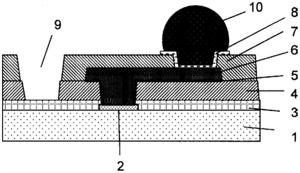
[图1]是表示具有凸块的半导体器件的焊盘部分的放大截面的图。[ FIG. 1 ] is a view showing an enlarged cross-section of a pad portion of a semiconductor device having bumps.
[图2]是表示具有凸块的半导体器件的详细制作方法的图。[ Fig. 2 ] is a diagram illustrating a detailed method of manufacturing a semiconductor device having bumps.
[图3]是具有本发明的绝缘膜的半导体器件的焊盘部分的放大截面图。[ Fig. 3 ] is an enlarged sectional view of a pad portion of a semiconductor device having an insulating film of the present invention.
[图4]是具有本发明的绝缘膜的线圈部件的截面图。[ Fig. 4 ] is a sectional view of a coil component having an insulating film of the present invention.
具体实施方式Detailed ways
本发明为(A)碱溶性树脂,其特征在于,具有通式(1)表示的结构,且满足以下的(I)和(II),The present invention is (A) an alkali-soluble resin, characterized in that it has a structure represented by general formula (1), and satisfies the following (I) and (II),
(I)作为通式(1)的X1,具有碳原子数为8~30的脂肪族链的有机基团以相对于X1和X2的总量100摩尔%而言30~70摩尔%的量被含有,(I) As X 1 of the general formula (1), an organic group having an aliphatic chain having 8 to 30 carbon atoms is 30 to 70 mol% relative to 100 mol% of the total amount of X 1 and X 2 The amount is contained,
(II)作为通式(1)的Y1,具有二苯醚结构的有机基团以相对于Y1和Y2的总量100摩尔%而言1~30摩尔%的量被含有,(II) As Y 1 of the general formula (1), an organic group having a diphenyl ether structure is contained in an amount of 1 to 30 mol % relative to 100 mol % of the total amount of Y 1 and Y 2 ,
[化学式2][chemical formula 2]

(通式(1)中的X1表示碳原子数为2~100个的2价有机基团,Y1和Y2表示碳原子数为2~100个的2~6价有机基团,X2表示碳原子数为2~100个的4价有机基团,p和q表示0~4的范围的整数,n1和n2表示5~100000的范围的整数。)。( X in the general formula (1) represents a divalent organic group with 2 to 100 carbon atoms, Y 1 and Y 2 represent a 2 to 6 valent organic group with 2 to 100 carbon atoms, and X 2 represents a tetravalent organic group having 2 to 100 carbon atoms, p and q represent integers ranging from 0 to 4, and n1 and n2 represent integers ranging from 5 to 100000.).
在本发明中,所谓碱溶性,是指溶解速度为50nm/分钟以上。详细而言,是指:在硅晶片上涂布在γ-丁内酯中溶解有树脂而得的溶液,于120℃进行4分钟的预烘烤而形成膜厚为10μm±0.5μm的预烘烤膜,将前述预烘烤膜在23±1℃的2.38质量%四甲基氢氧化铵水溶液中浸渍1分钟后,利用纯水进行冲洗处理,由此时的膜厚减少求出的溶解速度为50nm/分钟以上。In the present invention, alkali solubility means that the dissolution rate is 50 nm/minute or more. Specifically, it refers to: apply a solution obtained by dissolving resin in γ-butyrolactone on a silicon wafer, and perform prebaking at 120°C for 4 minutes to form a prebaked film with a film thickness of 10μm±0.5μm. For the baked film, the aforementioned prebaked film was immersed in 2.38% by mass tetramethylammonium hydroxide aqueous solution at 23±1°C for 1 minute, then rinsed with pure water, and the dissolution rate obtained from the decrease in film thickness at this time 50nm/minute or more.
本发明的通式(1)表示的(A)碱溶性树脂是聚酰胺结构与聚酰亚胺结构共聚而得的树脂。前述聚酰胺结构是两组氨基与羟基相互位于邻位的苯并噁唑前体、其他聚羟基酰胺、聚酰胺、或它们的共聚物。另外,前述聚酰亚胺结构是使聚酰胺酸、聚酰胺酸酯进行脱水闭环而得的聚酰亚胺、或树脂末端被酰亚胺密封而得的结构。The (A) alkali-soluble resin represented by the general formula (1) of the present invention is a resin obtained by copolymerizing a polyamide structure and a polyimide structure. The aforementioned polyamide structure is a benzoxazole precursor, other polyhydroxyamides, polyamides, or their copolymers in which two groups of amino groups and hydroxyl groups are located in ortho positions. In addition, the said polyimide structure is the polyimide obtained by dehydrating and ring-closing polyamic acid and polyamic acid ester, or the structure which sealed the end of resin with imide.
通过具有聚酰胺结构,从而能够提高形成固化膜时的伸长率。By having a polyamide structure, the elongation at the time of forming a cured film can be improved.
另外,通过具有聚酰亚胺结构,与聚酰胺结构单质的情况相比,与金属的相互作用得以提高,形成固化膜时能够提高与金属的密合性。Moreover, by having a polyimide structure, the interaction with a metal improves compared with the case of a simple polyamide structure, and when forming a cured film, the adhesiveness with a metal can be improved.
在本发明的(A)碱溶性树脂仅满足(I)的情况下,通过聚酰胺结构中的柔软的脂肪族基团而能够获得高伸长率、低弹性的固化膜。但是,在聚酰胺为具有聚苯并噁唑前体结构的聚羟基酰胺的情况下,即,在(A)碱溶性树脂包含具有聚苯并噁唑前体结构的聚羟基酰胺的情况下,由于热处理时的聚苯并噁唑结构的闭环率同时上升,膜收缩变大,因此,固化膜的低应力性容易变得不充分。在(A)碱溶性树脂仅满足(II)的情况下,通过二苯醚结构而可得到高金属密合、高耐热的固化膜,但是无法获得低弹性,低应力性容易变得不充分。通过(A)碱溶性树脂处于满足(I)和(II)的范围,从而能够抑制由闭环所导致的膜收缩,且可实现由低弹性化所带来的大幅的低应力化。可认为其原因在于,二苯醚的刚性结构抑制了脂肪族链的柔软的运动。When the (A) alkali-soluble resin of the present invention satisfies only (I), a cured film with high elongation and low elasticity can be obtained due to the soft aliphatic group in the polyamide structure. However, when the polyamide is a polyhydroxyamide having a polybenzoxazole precursor structure, that is, when the (A) alkali-soluble resin contains a polyhydroxyamide having a polybenzoxazole precursor structure, Since the ring closure rate of the polybenzoxazole structure increases at the same time during the heat treatment, the shrinkage of the film increases, and thus the low stress property of the cured film tends to be insufficient. When (A) alkali-soluble resin satisfies only (II), a cured film with high metal adhesion and high heat resistance can be obtained due to the diphenyl ether structure, but low elasticity cannot be obtained, and low stress property tends to be insufficient . When the (A) alkali-soluble resin is in a range satisfying (I) and (II), shrinkage of the film due to ring closure can be suppressed, and significant stress reduction due to low elasticity can be achieved. This is considered to be because the rigid structure of diphenyl ether suppresses the soft movement of the aliphatic chain.
从得到高伸长率、低弹性的固化膜的观点考虑,具有碳原子数为8~30的脂肪族基团的有机基团相对于通式(1)的X1与X2的总量100摩尔%而言为30摩尔%以上,优选为40摩尔%以上,更优选为45摩尔%以上。从得到显影后的残膜率高、具有耐热性的固化膜的观点考虑,为70摩尔%以下,更优选为65摩尔%以下,进一步优选为60摩尔%以下。From the viewpoint of obtaining a cured film with high elongation and low elasticity, the organic group having an aliphatic group with 8 to 30 carbon atoms is 100% of the total amount of X1 and X2 in the general formula (1). The mol% is 30 mol% or more, preferably 40 mol% or more, more preferably 45 mol% or more. It is 70 mol% or less, more preferably 65 mol% or less, and still more preferably 60 mol% or less from the viewpoint of obtaining a heat-resistant cured film with a high residual film rate after development.
从得到闭环率得以抑制、金属密合性、耐热性高的固化膜的观点考虑,具有二苯醚结构的有机基团的含量相对于通式(1)的Y1与Y2的总量100摩尔%而言为1摩尔%以上,优选为5%以上,更优选为10%以上。从得到碱溶性,得到高伸长率、低弹性的固化膜的观点考虑,为30摩尔%以下,优选为25%以下,更优选为20%以下。From the viewpoint of obtaining a cured film with suppressed ring closure rate, metal adhesion, and high heat resistance, the content of the organic group having a diphenyl ether structure relative to the total amount of Y1 and Y2 in the general formula (1) 100 mol% is 1 mol% or more, Preferably it is 5% or more, More preferably, it is 10% or more. From the viewpoint of obtaining alkali solubility, high elongation, and low elasticity cured film, it is 30 mol% or less, preferably 25% or less, more preferably 20% or less.
通式(1)中的n1、n2表示通式(1)表示的结构中的摩尔比,n1、n2各自表示聚酰胺结构,聚酰亚胺结构的摩尔比。为了获得具有良好加工性的树脂组合物、具有高伸长率、低弹性模量、高密合性、耐热性的固化膜,优选n1、n2处于以下的(III)的范围。n 1 and n 2 in the general formula (1) represent the molar ratio in the structure represented by the general formula (1), and n 1 and n 2 each represent the molar ratio of the polyamide structure and the polyimide structure. In order to obtain a resin composition having good processability, and a cured film having high elongation, low elastic modulus, high adhesion, and heat resistance, n 1 and n 2 are preferably in the following range (III).
(III)通式(1)中的n1与n2满足n1/n2=10~20。(III) n 1 and n 2 in the general formula (1) satisfy n 1 /n 2 =10-20.
从由聚酰胺结构带来的适度的碱溶性、可得到具有高伸长率和低弹性模量的固化膜的观点考虑,优选n1/n2=10以上,更优选为15以上。从能够得到具有由聚酰亚胺结构带来的高金属密合性、耐热性的固化膜的观点考虑,优选为n1/n2=20以下。From the viewpoint of moderate alkali solubility due to the polyamide structure, and a cured film having high elongation and low elastic modulus, n 1 /n 2 =10 or more is preferable, and 15 or more is more preferable. From the viewpoint of obtaining a cured film having high metal adhesion and heat resistance due to the polyimide structure, n 1 /n 2 =20 or less is preferable.
n1、n2能够在使用核磁共振装置(NMR)对得到的树脂、树脂组合物、固化膜中的聚酰胺结构、酰亚胺结构的峰进行检测的方法进行确认。在由树脂单质进行分析的情况下,能够通过在1H-NMR光谱中针对各单体成分所固有的峰算出面积比而进行确认。在由树脂组合物、固化膜进行分析的情况下,利用有机溶剂进行提取、浓缩,并同样地算出NMR峰面积比。在无法利用有机溶剂进行提取的情况下,能够通过利用红外吸收光谱算出聚酰胺结构、酰亚胺结构的峰强度比而进行确认。需要说明,在进行聚合时使用的单体的摩尔比已知的情况下,能够由单体的配合摩尔比算出。n 1 and n 2 can be confirmed by a method of detecting the peaks of the polyamide structure and the imide structure in the obtained resin, resin composition, and cured film using a nuclear magnetic resonance apparatus (NMR). In the case of analyzing the resin alone, it can be confirmed by calculating the area ratio of peaks specific to each monomer component in the 1 H-NMR spectrum. When analyzing from a resin composition or a cured film, it extracts and concentrates with an organic solvent, and calculates NMR peak area ratio similarly. When extraction with an organic solvent is not possible, it can be confirmed by calculating the peak intensity ratio of the polyamide structure and the imide structure from infrared absorption spectrum. In addition, when the molar ratio of the monomer used at the time of superposition|polymerization is known, it can calculate from the compounding molar ratio of a monomer.
通式(1)中的重复单元的排列可以是嵌段方式,也可以是无规方式,但若将聚酰胺单元与聚酰亚胺单元进行嵌段共聚,则容易得到由聚酰胺带来的高伸长率、低弹性的特性和由聚酰亚胺带来的金属密合的特性,因此更优选。The arrangement of the repeating units in the general formula (1) can be block or random, but if the polyamide unit and the polyimide unit are block-copolymerized, it is easy to obtain the polyamide brought High elongation, low elasticity properties, and metal adhesion properties due to polyimide are more preferable.
从低弹性化和耐热性的观点出发,本发明的(A)碱溶性树脂中含有的碳原子数为8~30的脂肪族链优选为直链烷基。作为具有这样的直链烷基的羧酸或羧酸衍生物的具体例,可使用辛二酸、十二氟辛二酸、壬二酸、癸二酸、十六氟癸二酸、1,9-壬二酸、十二烷二酸、十三烷二酸、十四烷二酸、十五烷二酸、十六烷二酸、十七烷二酸、十八烷二酸、十九烷二酸、二十烷二酸、二十一烷二酸、二十二烷二酸、二十三烷二酸、二十四烷二酸、二十五烷二酸、二十六烷二酸、二十七烷二酸、二十八烷二酸、二十九烷二酸、三十烷二酸等脂肪族二羧酸、将它们的羧酸基利用下述通式所示的活性羧酸基进行取代而得的化合物。The aliphatic chain having 8 to 30 carbon atoms contained in the (A) alkali-soluble resin of the present invention is preferably a linear alkyl group from the viewpoint of low elasticity and heat resistance. As specific examples of carboxylic acids or carboxylic acid derivatives having such linear alkyl groups, suberic acid, dodecafluorosuberic acid, azelaic acid, sebacic acid, hexadecafluorosebacic acid, 1, 9-Azelaic acid, dodecanedioic acid, tridecanedioic acid, tetradecanedioic acid, pentadecanedioic acid, hexadecanedioic acid, heptadecanedioic acid, octadecanedioic acid, nonadecanedioic acid Alkanedioic acid, eicosanedioic acid, eicosanedioic acid, docosanedioic acid, tricosanedioic acid, tetradecanedioic acid, pentadecanedioic acid, hexacanedioic acid aliphatic dicarboxylic acids such as acid, heptacanedioic acid, octacosanedioic acid, nonacosanedioic acid, triacanedioic acid, etc., and their carboxylic acid groups are used for the activity shown in the following general formula A compound obtained by substituting a carboxylic acid group.
[化学式3][chemical formula 3]

式中,B及C可各自独立地列举氢原子、甲基、乙基、丙基、异丙基、叔丁基、三氟甲基、卤素基、苯氧基、硝基等,但并不限定于它们。In the formula, B and C can each independently include a hydrogen atom, methyl, ethyl, propyl, isopropyl, tert-butyl, trifluoromethyl, halogen, phenoxy, nitro, etc., but not limited to them.
其中,优选使用氯化物化合物以外的活性羧酸基。通过使用氯化物化合物以外的活性羧酸基,从而能够减少得到的树脂中的氯离子,防止因存在氯离子所引起的从金属基板的剥离。另外,作为活性羧酸基,进一步优选使用二咪唑(diimidazolide)化合物。二咪唑化合物的离去基团成为水溶性咪唑,因此能够利用水对得到的树脂进行再沉淀、清洗。进而,离去的咪唑为碱性,因此,在使聚酰亚胺前体结构进行共聚的情况下,在聚合时作为聚酰亚胺前体结构的闭环促进剂而发挥作用,在利用聚合反应制造树脂时,能够将一部分聚酰亚胺前体进行酰亚胺化。Among them, active carboxylic acid groups other than chloride compounds are preferably used. By using active carboxylic acid groups other than chloride compounds, chloride ions in the obtained resin can be reduced, and peeling from the metal substrate due to the presence of chloride ions can be prevented. Moreover, it is more preferable to use a diimidazole (diimidazolide) compound as an active carboxylic acid group. Since the leaving group of the diimidazole compound becomes a water-soluble imidazole, the obtained resin can be reprecipitated and washed with water. Furthermore, the released imidazole is basic, so when the polyimide precursor structure is copolymerized, it functions as a ring-closing accelerator of the polyimide precursor structure during polymerization. When manufacturing resin, a part of polyimide precursor can be imidized.
另外,作为在(A)碱溶性树脂中使用的具有二苯醚结构的二胺,可列举3,4’-二氨基二苯醚、4,4’-二氨基二苯醚、双{4-(4-氨基苯氧基)苯基}醚、向它们导入羟基而得的化合物,这些之中,特别优选为4,4-二氨基二苯醚。In addition, examples of the diamine having a diphenyl ether structure used in the (A) alkali-soluble resin include 3,4'-diaminodiphenyl ether, 4,4'-diaminodiphenyl ether, bis{4- Among (4-aminophenoxy)phenyl} ethers and compounds having hydroxyl groups introduced thereto, 4,4-diaminodiphenyl ether is particularly preferred.
关于本发明的通式(1)表示的(A)碱溶性树脂,作为Y1或Y2,优选通式(2)表示的聚醚结构以相对于Y1和Y2的总量100摩尔%而言1~20摩尔%的量被含有。Regarding the (A) alkali-soluble resin represented by the general formula (1) of the present invention, as Y1 or Y2 , the polyether structure represented by the general formula (2) is preferably 100 mol% relative to the total amount of Y1 and Y2 In other words, it is contained in an amount of 1 to 20 mol%.
[化学式4][chemical formula 4]

通式(2)中,R1~R4各自独立地表示碳原子数为2~10的亚烷基,a、b和c各自表示1≤a≤20、0≤b≤20、0≤c≤20的范围内的整数,重复单元的排列可以是嵌段方式,也可以是无规方式。另外,通式(2)中,*表示化学键。In the general formula (2), R 1 to R 4 each independently represent an alkylene group with 2 to 10 carbon atoms, and a, b and c each represent 1≤a≤20, 0≤b≤20, 0≤c An integer within the range of ≤20, and the arrangement of repeating units can be block or random. In addition, in the general formula (2), * represents a chemical bond.
从固化膜的高伸长率化和低弹性模量化的观点考虑,通式(2)表示的聚醚结构相对于通式(1)的Y1和Y2的总量100摩尔%而言优选为1摩尔%以上,更优选为5摩尔%以上。从得到耐热性高的固化膜的观点考虑,优选为20摩尔%以下。From the viewpoint of high elongation and low elastic modulus of the cured film, the polyether structure represented by the general formula (2) is 100 mol% relative to the total amount of Y1 and Y2 of the general formula (1) Preferably it is 1 mol% or more, More preferably, it is 5 mol% or more. From the viewpoint of obtaining a cured film with high heat resistance, it is preferably 20 mol% or less.
作为具有聚醚结构的二胺的具体例,可列举1,2-双(2-氨基乙氧基)乙烷、“JEFFAMINE”(注册商标)HK-511、ED-600、ED-900、ED-2003、EDR-148、EDR-176、D-200、D-400、D-2000、D-4000、“ELASTAMINE”(注册商标)RP-409、RP-2009、RT-1000、HT-1100、HE-1000、HT-1700(以上,HUNTSMAN(株)制)。其中,四亚甲基醚基的耐热性优异,因此能够赋予可靠性后的金属密合性,因此优选。作为例子,可列举RT-1000、HE-1000、HT-1100、HT-1700。Specific examples of diamines having a polyether structure include 1,2-bis(2-aminoethoxy)ethane, "JEFFAMINE" (registered trademark) HK-511, ED-600, ED-900, ED -2003, EDR-148, EDR-176, D-200, D-400, D-2000, D-4000, "ELASTAMINE" (registered trademark) RP-409, RP-2009, RT-1000, HT-1100, HE-1000, HT-1700 (above, manufactured by Huntsman Co., Ltd.). Among them, the tetramethylene ether group is excellent in heat resistance, and therefore it can provide reliable metal adhesion, and is therefore preferable. Examples include RT-1000, HE-1000, HT-1100, and HT-1700.
关于本发明的(A)碱溶性树脂的重均分子量(Mw),利用凝胶渗透色谱法(GPC)按照聚苯乙烯换算,将展开剂设为99.3质量%的N-甲基-2-吡咯烷酮、0.2质量%的氯化锂、0.5质量%的磷酸时,如果Mw为3000以上,则易于通过加热处理获得固化膜,为了得到具有高伸长率、耐热性的固化膜,更优选为10000以上,进一步优选为30000以上。另外,如果为200000以下,则能够作为感光性树脂来进行加工,为了得到良好的图案加工性,更优选为100000以下,进一步优选为70000以下。Regarding the weight-average molecular weight (Mw) of the (A) alkali-soluble resin of the present invention, the developer is 99.3% by mass of N-methyl-2-pyrrolidone in terms of polystyrene by gel permeation chromatography (GPC). , 0.2% by mass of lithium chloride, and 0.5% by mass of phosphoric acid, if Mw is 3000 or more, then it is easy to obtain a cured film by heat treatment, and in order to obtain a cured film with high elongation and heat resistance, it is more preferably 10000 or more, and more preferably 30,000 or more. Moreover, if it is 200000 or less, it can be processed as a photosensitive resin, and in order to obtain favorable pattern processability, it is more preferable that it is 100000 or less, and it is still more preferable that it is 70000 or less.
关于可以在本发明的(A)碱溶性树脂中使用的上述以外的二羧酸、二羧酸衍生物、酸二酐以及二胺,可以使用已知的物质。Known dicarboxylic acids, dicarboxylic acid derivatives, acid dianhydrides, and diamines other than the above that can be used for (A) alkali-soluble resin of the present invention can be used.
作为酸二酐,具体而言,可列举均苯四酸二酐,3,3’,4,4’-联苯四甲酸二酐,3,3’,4,4’-二苯甲酮四甲酸二酐,双(3,4-二羧基苯基)磺酸二酐,3,3’,4,4’-二苯醚四甲酸二酐等芳香族四羧酸二酐、或将这些化合物的氢原子利用烷基或卤素原子进行取代而得的化合物;1,2,3,4-环丁烷四甲酸二酐、1,2,4,5-环己烷四甲酸二酐、双环[2.2.2]辛-7-烯-2,3,5,6-四甲酸二酐、3,4-二羧基-1,2,3,4-四氢-1-萘琥珀酸二酐这样的脂环式、半脂环式四羧酸二酐等,但并不限于它们。As the acid dianhydride, specifically, pyromellitic dianhydride, 3,3',4,4'-biphenyltetracarboxylic dianhydride, 3,3',4,4'-benzophenone tetra Aromatic tetracarboxylic dianhydrides such as formic dianhydride, bis(3,4-dicarboxyphenyl)sulfonic dianhydride, 3,3',4,4'-diphenyl ether tetracarboxylic dianhydride, or these
作为二羧酸,除了与由上述酸二酐得到的聚合物的酸二酐残基相同的结构以外,还可以使用具有下述结构的二羧酸或将这些二羧酸的羧酸基利用前述活性羧酸基进行取代而得的化合物作为二羧酸衍生物。As the dicarboxylic acid, in addition to the same structure as the acid dianhydride residue of the polymer obtained from the above-mentioned acid dianhydride, dicarboxylic acids having the following structures can also be used or the carboxylic acid groups of these dicarboxylic acids can be used by the aforementioned A compound obtained by substituting an active carboxylic acid group is referred to as a dicarboxylic acid derivative.
[化学式5][chemical formula 5]

[化学式6][chemical formula 6]

*表示键。* means key.
作为二胺,具体而言,可列举双(3-氨基-4-羟基苯基)丙烷、双(3-氨基-4-羟基)联苯等含羟基的二胺;3-磺酸-4,4’-二氨基二苯醚等含磺酸的二胺;二巯基苯二胺等含硫醇基的二胺;或具有下述所示的结构的芳香族二胺、将它们的芳香族环的一部分氢原子利用碳原子数为1~10的烷基、氟烷基、卤素原子等进行取代而得的化合物;环己二胺、亚甲基双环己胺等脂环式二胺;等等,但不限定于它们。这些二胺可以直接使用,或以对应的二异氰酸酯化合物、三甲基甲硅烷基化二胺的形式来使用。在得到高碱溶性的方面,优选在二胺总量中使用50摩尔%以上的前述含羟基的二胺。Specific examples of the diamine include hydroxyl-containing diamines such as bis(3-amino-4-hydroxyphenyl)propane and bis(3-amino-4-hydroxy)biphenyl; 3-sulfonic acid-4, sulfonic acid-containing diamines such as 4'-diaminodiphenyl ether; thiol-containing diamines such as dimercaptophenylenediamine; or aromatic diamines having the structures shown below, and their aromatic rings A compound obtained by substituting a part of the hydrogen atoms with an alkyl group having 1 to 10 carbon atoms, a fluoroalkyl group, a halogen atom, etc.; alicyclic diamines such as cyclohexanediamine and methylenebicyclohexylamine; etc. , but not limited to them. These diamines can be used as they are or in the form of corresponding diisocyanate compounds and trimethylsilylated diamines. In order to obtain high alkali solubility, it is preferable to use 50 mol% or more of the said hydroxyl group-containing diamines in the total amount of diamines.
[化学式7][chemical formula 7]

[化学式8][chemical formula 8]

另外,可以在不使耐热性降低的范围内共聚具有硅氧烷结构的脂肪族二胺,能够提高与硅基板的粘接性。具体而言,可列举在全部二胺中共聚1~15摩尔%的双(3-氨基丙基)四甲基二硅氧烷、双(对氨基苯基)八甲基五硅氧烷等而得的共聚物等。In addition, aliphatic diamine having a siloxane structure can be copolymerized within a range not to lower heat resistance, and adhesiveness to a silicon substrate can be improved. Specifically, bis(3-aminopropyl)tetramethyldisiloxane, bis(p-aminophenyl)octamethylpentasiloxane, etc., which are copolymerized in an amount of 1 to 15 mol% in all diamines are mentioned. obtained copolymers, etc.
本发明的(A)碱溶性树脂优选利用单胺、酸酐、单羧酸、单酰氯化合物、单活性酯化合物等封端剂对主链末端进行密封。通过对末端进行密封,从而能够提高用作感光性树脂组合物时的保存稳定性。另外,通过利用具有羟基、羧基、磺酸基、硫醇基、乙烯基、乙炔基或烯丙基的封端剂进行密封,从而能够易于将用作感光性树脂组合物时的(A)碱溶性树脂在碱溶液中的溶解速度、得到的固化膜的机械特性调整至优选的范围。封端剂的导入比例相对于全部胺成分而言优选为0.1~50摩尔%,通过处于该范围,从而能够在不使树脂的分子量降低的情况下使保存稳定性、机械特性提高。In the (A) alkali-soluble resin of the present invention, it is preferable to seal the end of the main chain with an end-capping agent such as a monoamine, an acid anhydride, a monocarboxylic acid, a monoacyl chloride compound, or a monoactive ester compound. By sealing the terminal, the storage stability when used as a photosensitive resin composition can be improved. In addition, by sealing with a terminal blocking agent having a hydroxyl group, a carboxyl group, a sulfonic acid group, a thiol group, a vinyl group, an ethynyl group or an allyl group, it is possible to easily use the (A) base when used as a photosensitive resin composition. The dissolution rate of the soluble resin in the alkali solution and the mechanical properties of the obtained cured film are adjusted to a preferable range. The introduction ratio of the end-blocking agent is preferably 0.1 to 50 mol% with respect to the total amine components, and by being within this range, storage stability and mechanical properties can be improved without reducing the molecular weight of the resin.
作为单胺、酸酐、单羧酸、单酰氯化合物、单活性酯化合物,可以使用已知的物质。Known ones can be used as the monoamine, acid anhydride, monocarboxylic acid, monoacyl chloride compound, and monoactive ester compound.
本发明中使用的封端剂可以利用以下方法容易地进行检测。例如,将导入有封端剂的树脂溶解在酸性溶液中,分解为作为结构单元的胺成分和酸酐成分,并利用气相色谱(GC)、NMR对其进行测定,从而能够容易地对本发明中使用的封端剂进行检测。除此以外,可以利用热解气相色谱(PGC)、红外光谱以及13C-NMR光谱直接对导入有封端剂的树脂成分进行测定,由此也能够容易地进行检测。The blocking agent used in the present invention can be easily detected by the following method. For example, the resin into which the end-blocking agent is introduced is dissolved in an acidic solution, decomposed into amine components and acid anhydride components as structural units, and measured by gas chromatography (GC) or NMR, so that it can be easily used in the present invention. The blocking agent is detected. In addition, the resin component into which the end-blocking agent has been introduced can be directly measured by pyrolysis gas chromatography (PGC), infrared spectroscopy, and 13 C-NMR spectroscopy, thereby enabling easy detection.
本发明中使用的(A)碱溶性树脂例如可以通过以下的方法来合成,但不限定于此。(A) Alkali-soluble resin used for this invention can be synthesize|combined by the following method, for example, However, It is not limited to this.
首先,将二羧酸或利用活性羧酸基对二羧酸进行取代而得的化合物与二胺于室温、根据情况在经提高的温度下溶解在有机溶剂中,接下来进行加热而使其聚合。从反应时的溶液的稳定性的观点考虑,进行溶解的顺序优选先溶解溶解性高的二胺化合物。然后,加入酸二酐,根据情况加入其它共聚成分,加入作为封端剂的酸或酸酐,使它们进行聚合。First, a dicarboxylic acid or a compound obtained by substituting a dicarboxylic acid with an active carboxylic acid group and a diamine are dissolved in an organic solvent at room temperature or at an elevated temperature depending on the case, and then heated to polymerize . From the viewpoint of the stability of the solution during the reaction, the order of dissolution is preferably to dissolve the diamine compound with high solubility first. Then, an acid dianhydride is added, and other copolymerization components are added as the case may be, and an acid or an acid anhydride as a terminal blocking agent is added to polymerize them.
在导入具有脂肪族基团的二胺的情况下,利用活性羧酸基对二羧酸进行取代而得的化合物与二胺化合物的反应优选在70~100℃下进行。When introducing the diamine which has an aliphatic group, it is preferable to perform reaction of the compound which substituted dicarboxylic acid with an active carboxylic acid group, and a diamine compound at 70-100 degreeC.
关于聚酰胺结构,是上述聚合法中来自二羧酸或利用活性羧酸基对二羧酸进行取代而得的化合物的结构。The polyamide structure is a structure derived from a dicarboxylic acid or a compound obtained by substituting a dicarboxylic acid with an active carboxylic acid group in the above-mentioned polymerization method.
关于聚酰亚胺结构,是上述聚合法中来自酸二酐的结构,能够利用下述方法进行合成:在聚合中得到聚酰胺酸或利用酯化剂使羧酸进行反应而得的聚酰胺酸酯结构,进而使其在反应体系中进行脱水闭环,由此,得到聚酰亚胺的方法;使具有酰亚胺结构的单体进行反应的方法;通过混合聚酰亚胺聚合物而导入酰亚胺结构的方法。Regarding the polyimide structure, it is a structure derived from acid dianhydride in the above-mentioned polymerization method, and can be synthesized by the following method: Polyamic acid obtained by polymerization or polyamic acid obtained by reacting carboxylic acid with an esterifying agent ester structure, and then make it undergo dehydration and ring closure in the reaction system, thereby obtaining a method of polyimide; a method of reacting a monomer with an imide structure; introducing an imide by mixing a polyimide polymer Method of imine structure.
关于本发明中使用的(A)碱溶性树脂,优选在利用上述方法进行聚合后,投入到大量的水或甲醇和水的混合液等中,使其沉淀,进行过滤干燥,从而进行分离。干燥温度优选为40~100℃,更优选为50~80℃。通过该操作能够除去未反应的单体、二聚物、三聚物等低聚物成分,使热固化后的膜特性提高。The (A) alkali-soluble resin used in the present invention is preferably polymerized by the above-mentioned method, poured into a large amount of water or a mixture of methanol and water, precipitated, filtered and dried, and isolated. The drying temperature is preferably 40 to 100°C, more preferably 50 to 80°C. By this operation, oligomer components such as unreacted monomers, dimers, and trimers can be removed, and film properties after thermosetting can be improved.
作为(A)碱溶性树脂的聚合中使用的有机溶剂,作为有机溶剂,例如可列举N,N-二甲基甲酰胺、N,N-二甲基乙酰胺、N-甲基-2-吡咯烷酮、1,3-二甲基-2-咪唑啉酮、N,N’-二甲基丙烯脲、N,N-二甲基异丁酸酰胺、N,N-二甲基乳酰胺、N,N-二甲基丙酰胺、甲氧基-N,N-二甲基丙酰胺的酰胺类;γ-丁内酯、γ-戊内酯、δ-戊内酯、γ-己内酯、ε-己内酯、α-甲基-γ-丁内酯等环状酯类;碳酸亚乙酯、碳酸亚丙酯等碳酸酯类;三乙二醇等二醇类;间甲酚、对甲酚等酚类;苯乙酮、环丁砜、二甲基亚砜、四氢呋喃、二甲基亚砜、丙二醇单甲醚乙酸酯,乳酸乙酯等,但不限定于这些。(A) As the organic solvent used for the polymerization of the alkali-soluble resin, examples of the organic solvent include N,N-dimethylformamide, N,N-dimethylacetamide, N-methyl-2-pyrrolidone , 1,3-dimethyl-2-imidazolidinone, N,N'-dimethylpropylene urea, N,N-dimethylisobutyric acid amide, N,N-dimethyllactamide, N, Amides of N-dimethylpropanamide, methoxy-N,N-dimethylpropanamide; γ-butyrolactone, γ-valerolactone, δ-valerolactone, γ-caprolactone, ε -Cyclic esters such as caprolactone and α-methyl-γ-butyrolactone; carbonates such as ethylene carbonate and propylene carbonate; glycols such as triethylene glycol; m-cresol, p-methyl Phenols such as phenol; acetophenone, sulfolane, dimethyl sulfoxide, tetrahydrofuran, dimethyl sulfoxide, propylene glycol monomethyl ether acetate, ethyl lactate, etc., but not limited to these.
本发明的(A)碱溶性树脂可以通过与(B)感光剂和(C)溶剂混合而作为感光性树脂组合物使用。(A) Alkali-soluble resin of this invention can be used as a photosensitive resin composition by mixing with (B) photosensitive agent and (C) solvent.
含有光产酸剂作为(B)感光剂的感光性树脂组合物可以用作正型感光性树脂组合物。另外,含有光聚合性化合物和光聚合引发剂作为感光剂的感光性树脂组合物可以用作负型感光性树脂组合物。A photosensitive resin composition containing a photoacid generator as (B) photosensitizer can be used as a positive photosensitive resin composition. In addition, a photosensitive resin composition containing a photopolymerizable compound and a photopolymerization initiator as a photosensitizer can be used as a negative photosensitive resin composition.
相较于负型感光性树脂组合物,正型感光性组合物的析像度优异,因此适于形成微细加工图案的用途。Since the resolution of a positive photosensitive composition is excellent compared with a negative photosensitive resin composition, it is suitable for the use which forms a microfabrication pattern.
作为正型感光性树脂组合物的光产酸剂,优选含有醌二叠氮化合物。作为醌二叠氮化合物,可举出二叠氮基醌的磺酸以酯方式键合于聚羟基化合物而得到的化合物;二叠氮基醌的磺酸以磺酰胺方式键合于多胺化合物而得到的化合物;二叠氮基醌的磺酸以酯方式及/或磺酰胺方式键合于聚羟基多胺化合物而得到的化合物等。这些聚羟基化合物、聚氨基化合物、聚羟基聚氨基化合物的全部的官能团可以不完全被二叠氮基醌取代,但优选平均地官能团全体的40摩尔%以上被二叠氮基醌取代。通过含有这样的醌二叠氮化合物,从而能够得到对作为通常的紫外线的汞灯的i射线(波长365nm)、h射线(波长405nm)、g射线(波长436nm)具有感光性的正型感光性树脂组合物。As a photoacid generator of a positive photosensitive resin composition, it is preferable to contain a quinone diazide compound. Examples of quinonediazide compounds include compounds in which sulfonic acid of quinonediazido is ester-bonded to a polyhydroxy compound; sulfonic acid of quinonediazido is bonded to polyamine compounds in a sulfonamide manner. The obtained compound; a compound in which sulfonic acid of quinonediazide is bonded to a polyhydroxypolyamine compound in an ester form and/or a sulfonamide form; and the like. All the functional groups of these polyhydroxy compounds, polyamino compounds, and polyhydroxy polyamino compounds may not be completely substituted by quinonediazide, but preferably 40 mol% or more of all the functional groups are substituted by quinonediazide on average. By containing such a quinonediazide compound, it is possible to obtain positive photosensitivity to i-rays (wavelength 365nm), h-rays (wavelength 405nm), and g-rays (wavelength 436nm) of a mercury lamp, which is a common ultraviolet ray. resin composition.
作为聚羟基化合物,具体而言,可列举Bis-Z、BisP-EZ、TekP-4HBPA、TrisP-HAP、TrisP-PA、TrisP-SA、TrisOCR-PA、BisOCHP-Z、BisP-MZ、BisP-PZ、BisP-IPZ、BisOCP-IPZ、BisP-CP、BisRS-2P、BisRS-3P、BisP-OCHP、Methylene Tris-FR-CR、BisRS-26X、DML-MBPC、DML-MBOC、DML-OCHP、DML-PCHP、DML-PC、DML-PTBP、DML-34X、DML-EP、DML-POP、Dimethylol-BisOC-P、DML-PFP、DML-PSBP、DML-MTrisPC、TriML-P、TriML-35XL、TML-BP、TML-HQ、TML-pp-BPF、TML-BPA、TMOM-BP、HML-TPPHBA、HML-TPHAP(以上,为商品名,本州化学工业制)、BIR-OC、BIP-PC、BIR-PC、BIR-PTBP、BIR-PCHP、BIP-BIOC-F、4PC、BIR-BIPC-F、TEP-BIP-A、46DMOC、46DMOEP、TM-BIP-A(以上,为商品名,旭有机材工业制)、2,6-二甲氧基甲基-4-叔丁基苯酚、2,6-二甲氧基甲基-对甲酚、2,6-二乙酰氧基甲基-对甲酚、萘酚、四羟基二苯甲酮、没食子酸甲酯、双酚A、双酚E、亚甲基双酚、BisP-AP(为商品名,本州化学工业制)、Novolac树脂等,但不限定于它们。Specific examples of the polyhydroxy compound include Bis-Z, BisP-EZ, TekP-4HBPA, TrisP-HAP, TrisP-PA, TrisP-SA, TrisOCR-PA, BisOCHP-Z, BisP-MZ, BisP-PZ , BisP-IPZ, BisOCP-IPZ, BisP-CP, BisRS-2P, BisRS-3P, BisP-OCHP, Methylene Tris-FR-CR, BisRS-26X, DML-MBPC, DML-MBOC, DML-OCHP, DML- PCHP, DML-PC, DML-PTBP, DML-34X, DML-EP, DML-POP, Dimethylol-BisOC-P, DML-PFP, DML-PSBP, DML-MTrisPC, TriML-P, TriML-35XL, TML- BP, TML-HQ, TML-pp-BPF, TML-BPA, TMOM-BP, HML-TPPHBA, HML-TPHAP (the above are trade names, manufactured by Honshu Chemical Industries), BIR-OC, BIP-PC, BIR- PC, BIR-PTBP, BIR-PCHP, BIP-BIOC-F, 4PC, BIR-BIPC-F, TEP-BIP-A, 46DMOC, 46DMOEP, TM-BIP-A (the above are trade names, Asahi Organic Materials Industry Co., Ltd. ), 2,6-dimethoxymethyl-4-tert-butylphenol, 2,6-dimethoxymethyl-p-cresol, 2,6-diacetoxymethyl-p-cresol , naphthol, tetrahydroxybenzophenone, methyl gallate, bisphenol A, bisphenol E, methylene bisphenol, BisP-AP (trade name, manufactured by Honshu Chemical Industries), Novolac resin, etc., but not limited to them.
作为聚氨基化合物,具体而言,可列举1,4-苯二胺、1,3-苯二胺、4,4’-二氨基二苯醚、4,4’-二氨基二苯基甲烷、4,4’-二氨基二苯基砜、4,4’-二氨基二苯基硫醚等,但不限定于它们。As the polyamino compound, specifically, 1,4-phenylenediamine, 1,3-phenylenediamine, 4,4'-diaminodiphenyl ether, 4,4'-diaminodiphenylmethane, 4,4'-diaminodiphenylsulfone, 4,4'-diaminodiphenylsulfide, etc., but not limited to them.
另外,作为聚羟基聚氨基化合物,具体而言,可列举2,2-双(3-氨基-4-羟基苯基)六氟丙烷、3,3’-二羟基联苯胺等,但不限定于它们。In addition, examples of the polyhydroxypolyamino compound specifically include 2,2-bis(3-amino-4-hydroxyphenyl)hexafluoropropane, 3,3'-dihydroxybenzidine, etc., but are not limited to they.
这些之中,醌二叠氮化合物优选包含与酚化合物及二叠氮基萘醌-4-磺酰基形成的酯。由此,可以在i射线曝光中得到高灵敏度和更高的析像度。Among these, the quinonediazide compound preferably includes an ester with a phenol compound and naphthoquinonediazide-4-sulfonyl group. Thereby, high sensitivity and higher resolution can be obtained in i-ray exposure.
本发明的感光性树脂组合物中使用的醌二叠氮化合物的含量相对于树脂100质量份而言优选为1~50质量份,更优选为10~40质量份。通过将醌二叠氮化合物的含量设为该范围,从而可得到曝光部与未曝光部的对比度,由此能够实现更高灵敏度化,因此优选。进而,可以根据需要添加敏化剂等。It is preferable that it is 1-50 mass parts with respect to 100 mass parts of resins, and, as for content of the quinone diazide compound used for the photosensitive resin composition of this invention, it is more preferable that it is 10-40 mass parts. By making content of a quinone diazide compound into this range, since the contrast of an exposure part and an unexposed part can be obtained and higher sensitivity can be achieved, it is preferable. Furthermore, a sensitizer etc. can be added as needed.
关于本发明的感光性树脂组合物,在含有光聚合性化合物和光聚合引发剂作为(B)感光剂的情况下,可以作为利用光进行不溶化的负型感光性树脂组合物使用。光聚合性化合物含有聚合性不饱和官能团。作为聚合性不饱和官能团,例如可列举乙烯基、烯丙基、丙烯酰基、甲基丙烯酰基等不饱和双键官能团、炔丙基等不饱和三键官能团。这些之中,在聚合性方面,优选为选自共轭型乙烯基、丙烯酰基和甲基丙烯酰基中的基团。When the photosensitive resin composition of this invention contains a photopolymerizable compound and a photoinitiator as (B) photosensitizer, it can be used as a negative photosensitive resin composition insolubilized by light. The photopolymerizable compound contains a polymerizable unsaturated functional group. Examples of the polymerizable unsaturated functional group include unsaturated double bond functional groups such as vinyl groups, allyl groups, acryloyl groups, and methacryloyl groups, and unsaturated triple bond functional groups such as propargyl groups. Among these, in terms of polymerizability, a group selected from a conjugated vinyl group, an acryloyl group, and a methacryloyl group is preferable.
另外,作为该官能团所含有的数量,从稳定性的方面考虑,优选为1~4,各个基团可以不同。另外,光聚合性化合物的数均分子量优选为30~800。如果数均分子量为30~800的范围,则与聚酰胺的相容性良好,树脂组合物溶液的稳定性良好。In addition, the number of the functional groups contained is preferably 1 to 4 from the viewpoint of stability, and may be different for each group. Moreover, it is preferable that the number average molecular weight of a photopolymerizable compound is 30-800. When the number average molecular weight is in the range of 30 to 800, the compatibility with the polyamide is good, and the stability of the resin composition solution is good.
作为光聚合性化合物,可以使用已知的物质。作为可特别优选使用的光聚合性化合物,可列举1,9-壬二醇二甲基丙烯酸酯、1,10-癸二醇二甲基丙烯酸酯、二羟甲基-三环癸烷二丙烯酸酯、季戊四醇三丙烯酸酯、季戊四醇四丙烯酸酯、季戊四醇三甲基丙烯酸酯、季戊四醇四甲基丙烯酸酯、亚甲基双丙烯酰胺、N,N-二甲基丙烯酰胺、N-羟甲基丙烯酰胺、2,2,6,6-四甲基哌啶基丙烯酸酯、N-甲基-2,2,6,6-四甲基哌啶基丙烯酸酯、环氧乙烷改性双酚A二丙烯酸酯、环氧乙烷改性双酚A二甲基丙烯酸酯、N-乙烯基吡咯烷酮、N-乙烯基己内酰胺等,但不限定于它们。As the photopolymerizable compound, known ones can be used. Particularly preferably used photopolymerizable compounds include 1,9-nonanediol dimethacrylate, 1,10-decanediol dimethacrylate, and dimethylol-tricyclodecane diacrylate. ester, pentaerythritol triacrylate, pentaerythritol tetraacrylate, pentaerythritol trimethacrylate, pentaerythritol tetramethacrylate, methylenebisacrylamide, N,N-dimethylacrylamide, N-methylolacrylamide , 2,2,6,6-tetramethylpiperidinyl acrylate, N-methyl-2,2,6,6-tetramethylpiperidinyl acrylate, ethylene oxide modified bisphenol A Acrylate, ethylene oxide-modified bisphenol A dimethacrylate, N-vinylpyrrolidone, N-vinylcaprolactam, etc., but not limited to them.
本发明的感光性树脂组合物中的光聚合性化合物的含量相对于树脂100质量份而言优选设为5~200质量份,从相容性的方面考虑,更优选设为5~150质量份。通过将光聚合性化合物的含量设为5质量份以上,从而能够防止显影时的曝光部的溶出,得到显影后的残膜率高的树脂组合物。另外,通过将光聚合性化合物的含量设为200质量份以下,从而能够抑制形成膜时的膜的白化。The content of the photopolymerizable compound in the photosensitive resin composition of the present invention is preferably 5 to 200 parts by mass with respect to 100 parts by mass of the resin, and more preferably 5 to 150 parts by mass from the viewpoint of compatibility. . By making content of a
作为将本发明的感光性树脂组合物用作负型感光性树脂组合物时的光聚合引发剂,可使用已知的物质。例如,可列举二苯甲酮、米蚩酮、4,4,-双(二乙基氨基)二苯甲酮等二苯甲酮类;3,5-双(二乙基氨基亚苄基)-N-甲基-4-哌啶酮等亚苄基类;7-二乙基氨基-3-噻吩甲酰基香豆素等香豆素类;2-叔丁基蒽醌等蒽醌类;苯偶姻甲基醚等苯偶姻类;乙二醇二(3-巯基丙酸酯)等巯基类;N-苯基甘氨酸等甘氨酸类;1-苯基-1,2-丁二酮-2-(邻甲氧基羰基)肟、双(α-As a photoinitiator when using the photosensitive resin composition of this invention as a negative photosensitive resin composition, a known thing can be used. For example, benzophenones such as benzophenone, Michler's ketone, and 4,4'-bis(diethylamino)benzophenone; 3,5-bis(diethylaminobenzylidene) -Benzylidene such as N-methyl-4-piperidone; coumarins such as 7-diethylamino-3-thienoylcoumarin; anthraquinones such as 2-tert-butylanthraquinone; Benzoins such as benzoin methyl ether; mercaptos such as ethylene glycol bis(3-mercaptopropionate); glycines such as N-phenylglycine; 1-phenyl-1,2-butanedione- 2-(o-methoxycarbonyl)oxime, bis(α-
异亚硝基苯丙酮肟)间苯二甲酰(bis(α-isonitrosopropiophenoneoxime)isophthal)、1,2-辛二酮-1-[4-(苯基硫基)苯基]-2-(邻苯甲酰基肟)、OXE02(商品名,CibaSpecialty Chemicals,Inc.制)、NCI-831(商品名,株式会社ADEKA制)等肟类;2-苄基-2-二甲基氨基-1-(4-吗啉代苯基)-丁烷-1-2-甲基-1[4-(甲基硫基)苯基]-2-吗啉代丙烷-1-酮等α-氨基烷基苯酮类等。这些之中,优选为上述肟类,特别优选为1-苯基-1,2-丙二酮-2-(邻乙氧基羰基)肟、1-苯基-1,2-丙二酮-2-(邻苯甲酰基)肟、双(α-异亚硝基苯丙酮肟)间苯二甲酰、1,2-辛二酮-1-[4-(苯基硫基)苯基]-2-(邻苯甲酰基肟)、OXE02、NCI-831。它们可以单独使用,或者可以组合使用2种以上。Isonitrosopropiophenoneoxime) isophthaloyl (bis(α-isonitrosopropiophenoneoxime) isophthal), 1,2-octanedione-1-[4-(phenylthio)phenyl]-2-(o Benzoyl oxime), OXE02 (trade name, manufactured by Ciba Specialty Chemicals, Inc.), NCI-831 (trade name, manufactured by ADEKA Corporation) and other oximes; 2-benzyl-2-dimethylamino-1-( 4-morpholinophenyl)-butane-1-2-methyl-1[4-(methylthio)phenyl]-2-morpholinopropan-1-one and other α-aminoalkylbenzenes Ketones etc. Among these, the above-mentioned oximes are preferable, and 1-phenyl-1,2-propanedione-2-(o-ethoxycarbonyl)oxime, 1-phenyl-1,2-propanedione- 2-(o-benzoyl)oxime, bis(α-isonitrosopropiophenone oxime)isophthaloyl, 1,2-octanedione-1-[4-(phenylthio)phenyl] -2-(o-benzoyl oxime), OXE02, NCI-831. These can be used individually or in combination of 2 or more types.
这些之中,从光反应的方面考虑,优选为选自上述二苯甲酮类、甘氨酸类、巯基类、肟类、α-氨基烷基苯酮类、2,2’-双(邻氯苯基)-4,4’,5,5’-四苯基双咪唑中的组合。Among these, from the viewpoint of photoreaction, preferably selected from the above-mentioned benzophenones, glycines, mercaptos, oximes, α-aminoalkylphenones, 2,2'-bis(o-chlorobenzene base)-4,4',5,5'-tetraphenylbiimidazole in combination.
光聚合引发剂的含量相对于(A)碱溶性树脂的总量100质量份而言优选为0.1~60质量份,更优选为0.2~40质量份。若为0.1质量份以上,则通过光照射而产生足够的自由基,灵敏度提高,在这点上优选,若为60质量份以下,则不会因产生过度的自由基而导致光未照射部发生固化,碱显影性提高。It is preferable that it is 0.1-60 mass parts with respect to 100 mass parts of total amounts of (A) alkali-soluble resin, and, as for content of a photoinitiator, it is more preferable that it is 0.2-40 mass parts. If it is 0.1 mass part or more, sufficient free radicals are generated by light irradiation, and the sensitivity is improved, and it is preferable in this point, and if it is 60 mass parts or less, then excessive free radicals will not be generated to cause light-unirradiated parts to occur. Curing improves alkali developability.
本发明的感光性树脂组合物含有(C)溶剂。作为溶剂,可列举N-甲基-2-吡咯烷酮、γ-丁内酯、γ-戊内酯、δ-戊内酯、N,N-二甲基甲酰胺、N,N-二甲基乙酰胺、二甲基亚砜、1,3-二甲基-2-咪唑啉酮、N,N’-二甲基丙烯脲、N,N-二甲基乳酰胺等非质子性极性溶剂;四氢呋喃、二氧杂环己烷、丙二醇单甲醚、丙二醇单乙醚、二乙二醇单乙醚等醚类;丙酮、甲基乙基酮、二异丁基酮等酮类;乙酸乙酯、乙酸丁酯、乙酸异丁酯、乙酸丙酯、丙二醇单甲醚乙酸酯、3-甲基-3-甲氧基丁基乙酸酯等酯类;乳酸乙酯、乳酸甲酯、二丙酮醇、3-甲基-3-甲氧基丁醇等醇类;甲苯、二甲苯等芳香族烃类等。可以含有它们中的2种以上。The photosensitive resin composition of this invention contains (C) solvent. Examples of solvents include N-methyl-2-pyrrolidone, γ-butyrolactone, γ-valerolactone, δ-valerolactone, N,N-dimethylformamide, N,N-dimethylacetamide Aprotic polar solvents such as amides, dimethyl sulfoxide, 1,3-dimethyl-2-imidazolidinone, N,N'-dimethylpropyleneurea, N,N-dimethyllactamide; Tetrahydrofuran, dioxane, propylene glycol monomethyl ether, propylene glycol monoethyl ether, diethylene glycol monoethyl ether and other ethers; acetone, methyl ethyl ketone, diisobutyl ketone and other ketones; ethyl acetate, acetic acid Butyl ester, isobutyl acetate, propyl acetate, propylene glycol monomethyl ether acetate, 3-methyl-3-methoxybutyl acetate and other esters; ethyl lactate, methyl lactate, diacetone alcohol , 3-methyl-3-methoxybutanol and other alcohols; toluene, xylene and other aromatic hydrocarbons, etc. Two or more of these may be contained.
为了使组合物溶解,(C)溶剂的含量优选以相对于100质量份(A)碱溶性树脂而言100质量份以上的量被含有,为了形成膜厚为1μm以上的涂膜,(C)溶剂的含量优选以相对于100质量份(A)碱溶性树脂而言1500质量份以下的量被含有。In order to dissolve the composition, the content of the (C) solvent is preferably contained in an amount of 100 parts by mass or more relative to 100 parts by mass of the (A) alkali-soluble resin. In order to form a coating film with a film thickness of 1 μm or more, (C) It is preferable that content of a solvent is contained in the quantity of 1500 mass parts or less with respect to 100 mass parts of (A) alkali-soluble resins.
在前述(C)溶剂中,本发明的感光性树脂组合物优选含有沸点为150~250℃且熔点为-30℃以下的(D)化合物。进而,优选(D)化合物的分子量为100以上。通过熔点为-30℃以下,从而提高冰点以下的低温下的固化膜的机械特性,能够使半导体设备等的可靠性试验中对于热循环试验的耐性提高。为了进一步提高可靠性试验耐性,更优选熔点为-45℃以下。通过沸点为150~250℃,从而在不使耐热性、耐药品性降低的范围内残留在热处理后的固化膜中,因此能够提高低温下的固化膜的机械特性。另外,在残留在热处理后的固化膜中的观点上,还优选分子量为100以上。It is preferable that the photosensitive resin composition of this invention contains the (D) compound which has a boiling point of 150-250 degreeC and a melting point of -30 degreeC or less among said (C) solvents. Furthermore, it is preferable that the molecular weight of (D) compound is 100 or more. When the melting point is -30° C. or lower, the mechanical properties of the cured film at low temperatures below freezing point can be improved, and the resistance to thermal cycle tests in reliability tests of semiconductor devices and the like can be improved. In order to further improve reliability test resistance, the melting point is more preferably -45°C or lower. When the boiling point is 150 to 250° C., it remains in the cured film after heat treatment within the range not to lower the heat resistance and chemical resistance, so that the mechanical properties of the cured film at low temperature can be improved. Moreover, it is also preferable that molecular weight is 100 or more from a viewpoint of remaining in the cured film after heat processing.
即,作为(D)化合物,优选沸点为150~250℃并且熔点超过-45℃且为-30℃以下、分子量为100以上的(D-1)化合物,更优选沸点为150~250℃且熔点为-45℃以下、分子量为100以上的(D-2)化合物。That is, the compound (D) is preferably a compound (D-1) having a boiling point of 150 to 250°C and a melting point of more than -45°C to -30°C or lower, and a molecular weight of 100 or more, more preferably a boiling point of 150 to 250°C and a melting point of It is -45 degreeC or less and (D-2) compound whose molecular weight is 100 or more.
从获得提高低温下的固化膜的机械特性的效果的观点考虑,在(C)溶剂100质量份中,(D)化合物优选为0.1质量份以上,更优选为10质量份以上。从能够获得良好的涂布性、和显影后的高残膜率的观点考虑,在(C)溶剂100质量份中,(D)化合物优选为50质量份以下,更优选为30质量份以下。From the viewpoint of obtaining the effect of improving the mechanical properties of the cured film at low temperature, the (D) compound is preferably 0.1 mass parts or more in 100 mass parts of (C) solvent, more preferably 10 mass parts or more. From the viewpoint of obtaining good coatability and a high residual film rate after development, the (D) compound is preferably 50 parts by mass or less, more preferably 30 parts by mass or less, in 100 parts by mass of the (C) solvent.
另外,热处理后的固化膜中的(D)化合物的含量优选为0.05~5000ppm。通过为0.05ppm以上,从而能够获得提高低温下的固化膜的机械特性的效果,更优选为0.1ppm以上。通过固化膜中的(D)化合物的含量为5000ppm以下,从而能够获得良好的耐热性。Moreover, it is preferable that content of the (D) compound in the cured film after heat processing is 0.05-5000 ppm. The effect of improving the mechanical characteristics of the cured film at low temperature can be acquired by being 0.05 ppm or more, More preferably, it is 0.1 ppm or more. Favorable heat resistance can be acquired by content of the (D) compound in a cured film being 5000 ppm or less.
作为(D-1)化合物,具体而言,可列举二丙酮醇(沸点167℃,熔点-44℃,分子量116.16),N,N-二甲基异丁基酰胺(沸点176℃,熔点-34℃,分子量115.18)等。其中,特别优选为N,N-二甲基异丁基酰胺。As (D-1) compound, specifically, diacetone alcohol (boiling point 167°C, melting point -44°C, molecular weight 116.16), N,N-dimethylisobutylamide (boiling point 176°C, melting point -34 ℃, molecular weight 115.18), etc. Among them, N,N-dimethylisobutylamide is particularly preferable.
作为(D-2)化合物,具体而言,可列举异丙基环己烷(沸点155℃,熔点-89℃,分子量126.24)、N-乙基苯胺(沸点206℃,熔点-64℃,分子量121.18)、间乙基甲苯(沸点161℃,熔点-96℃,分子量120.19)、对乙基甲苯(沸点162℃,熔点-62℃,分子量120.19)、3-甲氧基甲苯(沸点177℃,熔点-56℃,分子量122.16)、乙酸己酯(沸点171℃,熔点-81℃,分子量144.21)、乙酸苄酯(沸点215℃,熔点-52℃,分子量150.18)、乙二醇单丁醚(沸点171℃,熔点-70℃,分子量118.18)、乙二醇单乙醚乙酸酯(沸点156℃,熔点-62℃,分子量132.16)、乙二醇单丁醚乙酸酯(沸点192℃,熔点-64℃,分子量160.21)、二乙二醇乙基甲基醚(沸点176℃,熔点-72℃,分子量148.21)、二乙二醇单甲醚(沸点193℃,熔点-70℃,分子量120.20)、二乙二醇单丁醚(沸点231℃,熔点-68℃,分子量162.23)、3-乙氧基丙酸乙酯(沸点166℃,熔点-75℃,分子量146.19)、N,N-二甲基邻甲苯胺(沸点185℃,熔点-61℃,分子量135.21)、N,N-二甲基丙酰胺(沸点174℃,熔点-45℃,分子量101.15),3-甲氧基-N,N-二甲基丙酰胺(沸点215℃,熔点-49℃,分子量131.17),2-乙基1-己醇(沸点183℃,熔点-76℃,分子量130.23)、1-己醇(沸点157℃,熔点-52℃,分子量102.17)、壬烷(沸点151℃,熔点-54℃,分子量128.26)、3-甲基环己酮(沸点170℃,熔点-74℃,分子量112.17)、己酸乙酯(沸点168℃,熔点-68℃,分子量144.21)、庚酸乙酯(沸点186℃,熔点-66℃,分子量158.24)、丙二酸二甲酯(沸点181℃,熔点-62℃,分子量132.12)、丙二酸二乙酯(沸点199℃,熔点-51℃,分子量160.17)、3-甲基环己酮(沸点169℃,熔点-74℃,分子量112.17)等。这些之中,从提高机械特性的效果高、涂布性良好的方面考虑,优选为二乙二醇单丁醚(沸点231℃,熔点-68℃,分子量162.23)、N,N-二甲基丙酰胺(沸点174℃,熔点-45℃,分子量101.15)、3-甲氧基-N,N-二甲基丙酰胺(沸点215℃,熔点-49℃,分子量131.17)。As (D-2) compound, specifically, isopropylcyclohexane (boiling point 155°C, melting point -89°C, molecular weight 126.24), N-ethylaniline (boiling point 206°C, melting point -64°C, molecular weight 121.18), m-ethyltoluene (boiling point 161°C, melting point -96°C, molecular weight 120.19), p-ethyltoluene (boiling point 162°C, melting point -62°C, molecular weight 120.19), 3-methoxytoluene (boiling point 177°C, Melting point -56°C, molecular weight 122.16), hexyl acetate (boiling point 171°C, melting point -81°C, molecular weight 144.21), benzyl acetate (boiling point 215°C, melting point -52°C, molecular weight 150.18), ethylene glycol monobutyl ether ( Boiling point 171°C, melting point -70°C, molecular weight 118.18), ethylene glycol monoethyl ether acetate (boiling point 156°C, melting point -62°C, molecular weight 132.16), ethylene glycol monobutyl ether acetate (boiling point 192°C, melting point -64°C, molecular weight 160.21), diethylene glycol ethyl methyl ether (boiling point 176°C, melting point -72°C, molecular weight 148.21), diethylene glycol monomethyl ether (boiling point 193°C, melting point -70°C, molecular weight 120.20 ), diethylene glycol monobutyl ether (boiling point 231°C, melting point -68°C, molecular weight 162.23), ethyl 3-ethoxypropionate (boiling point 166°C, melting point -75°C, molecular weight 146.19), N,N- Dimethyl o-toluidine (boiling point 185°C, melting point -61°C, molecular weight 135.21), N,N-dimethylpropionamide (boiling point 174°C, melting point -45°C, molecular weight 101.15), 3-methoxy-N , N-dimethylpropanamide (boiling point 215°C, melting point -49°C, molecular weight 131.17), 2-ethyl 1-hexanol (boiling point 183°C, melting point -76°C, molecular weight 130.23), 1-hexanol (boiling point 157°C, melting point -52°C, molecular weight 102.17), nonane (boiling point 151°C, melting point -54°C, molecular weight 128.26), 3-methylcyclohexanone (boiling point 170°C, melting point -74°C, molecular weight 112.17), hexane Ethyl heptanoate (boiling point 168°C, melting point -68°C, molecular weight 144.21), ethyl heptanoate (boiling point 186°C, melting point -66°C, molecular weight 158.24), dimethyl malonate (boiling point 181°C, melting point -62°C , molecular weight 132.12), diethyl malonate (boiling point 199°C, melting point -51°C, molecular weight 160.17), 3-methylcyclohexanone (boiling point 169°C, melting point -74°C, molecular weight 112.17), etc. Among these, diethylene glycol monobutyl ether (boiling point 231°C, melting point -68°C, molecular weight 162.23), N,N-dimethyl Propionamide (boiling point 174°C, melting point -45°C, molecular weight 101.15), 3-methoxy-N,N-dimethylpropanamide (boiling point 215°C, melting point -49°C, molecular weight 131.17).
本发明的感光性树脂组合物除了(A)碱溶性树脂、(B)感光剂、(C)溶剂以外,还可以含有下述添加剂。The photosensitive resin composition of this invention may contain the following additives other than (A) alkali-soluble resin, (B) photosensitizer, (C) solvent.
通过含有抗氧化剂作为添加剂,从而能够提高可靠性评价后的固化后的膜的伸长率特性、与金属材料的密合性。作为抗氧化剂,可列举通式(3)表示的化合物。By containing an antioxidant as an additive, the elongation characteristic of the cured film after reliability evaluation, and the adhesiveness with a metal material can be improved. As an antioxidant, the compound represented by General formula (3) is mentioned.
[化学式9][chemical formula 9]

通式(3)中,R5表示氢原子或碳原子数为2以上的烷基,R6表示碳原子数为2以上的亚烷基。R7表示包含碳原子数为2以上的亚烷基、O原子、以及N原子中的至少任意种的1~4价有机基团。k表示1~4的整数。In the general formula (3), R 5 represents a hydrogen atom or an alkyl group having 2 or more carbon atoms, and R 6 represents an alkylene group having 2 or more carbon atoms. R 7 represents a 1-4 valent organic group including at least any one of an alkylene group having 2 or more carbon atoms, an O atom, and an N atom. k represents an integer of 1-4.
通式(3)表示的化合物抑制(A)碱溶性树脂的脂肪族基团、酚式羟基的氧化劣化。另外,能够通过对金属材料的防锈作用来抑制金属氧化。The compound represented by general formula (3) suppresses oxidation deterioration of the aliphatic group and phenolic hydroxyl group of (A) alkali-soluble resin. In addition, metal oxidation can be suppressed by an antirust effect on metal materials.
为了(A)碱溶性树脂和金属材料能够同时发挥作用,k更优选为2~4的整数。作为R7,可列举烷基、环烷基、烷氧基、烷基醚基、烷基甲硅烷基、烷氧基甲硅烷基、芳基、芳基醚基、羧基、羰基、烯丙基、乙烯基、杂环基、-O-、-NH-、-NHNH-、它们的组合等,可以进一步具有取代基。其中,从在显影液中的溶解性、金属密合性的方面考虑,优选具有烷基醚、-NH-,从与树脂的相互作用和形成金属络合物所带来的金属密合性的方面考虑,更优选为-NH-。In order that (A) the alkali-soluble resin and the metal material can function simultaneously, k is more preferably an integer of 2-4. Examples of R 7 include alkyl, cycloalkyl, alkoxy, alkyl ether, alkylsilyl, alkoxysilyl, aryl, aryl ether, carboxyl, carbonyl, allyl , vinyl, heterocyclic group, -O-, -NH-, -NHNH-, combinations thereof, etc., may further have a substituent. Among them, from the viewpoint of solubility in the developer and metal adhesion, those having alkyl ethers, -NH-, and metal adhesion due to the interaction with the resin and the formation of metal complexes are preferred. Considering the aspect, it is more preferably -NH-.
下述通式(3)表示的化合物可列举以下的化合物作为例子,但不限于下述结构。The compounds represented by the following general formula (3) include the following compounds as examples, but are not limited to the following structures.
[化学式10][chemical formula 10]

[化学式11][chemical formula 11]

[化学式12][chemical formula 12]

[化学式13][chemical formula 13]

另外,通式(3)表示的化合物的添加量相对于(A)碱溶性树脂而言优选为0.1~10质量份,更优选为0.5~5质量份。在添加量少于0.1质量份的情况下,难以获得可靠性后的伸长率特性、对于金属材料的密合性的提高效果,另外,在多于10质量份的情况下,由于与感光剂的相互作用,有可能导致树脂组合物的灵敏度降低。Moreover, it is preferable that the addition amount of the compound represented by General formula (3) is 0.1-10 mass parts with respect to (A) alkali-soluble resin, More preferably, it is 0.5-5 mass parts. When the amount added is less than 0.1 parts by mass, it is difficult to obtain the elongation characteristics after reliability and the effect of improving the adhesion to metal materials. interaction, which may lead to a decrease in the sensitivity of the resin composition.
通过含有热交联剂作为本发明的感光性树脂组合物的添加剂,从而能够进一步实现伸长率的提高以及低应力化。作为热交联剂,可列举通式(4)表示的化合物。By containing a thermal crosslinking agent as an additive of the photosensitive resin composition of this invention, the improvement of elongation and reduction of stress can be aimed at further. As a thermal crosslinking agent, the compound represented by General formula (4) is mentioned.
[化学式14][chemical formula 14]

通式(4)中,R9和R10各自独立地表示氢原子或甲基。R8为具有碳原子数为2以上的亚烷基的2价有机基团,可以为直链状、支链状以及环状中的任意者。In the general formula (4), R 9 and R 10 each independently represent a hydrogen atom or a methyl group. R 8 is a divalent organic group having an alkylene group having 2 or more carbon atoms, and may be any of linear, branched and cyclic.
R8可列举烷基、环烷基、烷氧基、烷基醚基、烷基甲硅烷基、烷氧基甲硅烷基、芳基、芳基醚基、羧基、羰基、烯丙基、乙烯基、杂环基、将它们组合而得的基团等,可以进一步具有取代基。R 8 can include alkyl, cycloalkyl, alkoxy, alkyl ether, alkyl silyl, alkoxy silyl, aryl, aryl ether, carboxyl, carbonyl, allyl, vinyl A group, a heterocyclic group, a group obtained by combining them, and the like may further have a substituent.
热交联剂自身具有柔软的亚烷基和刚性的芳香族基团,因此,具有耐热性,且可实现伸长率的提高以及低应力化。作为交联基团,可列举丙烯酰基、羟甲基、烷氧基甲基、环氧基,但不限定于它们。其中,从能够与树脂的酚式羟基进行反应,提高固化膜的耐热性的方面、和能够在不脱水的情况下进行反应的方面考虑,优选为环氧基。Since the thermal crosslinking agent itself has a flexible alkylene group and a rigid aromatic group, it has heat resistance, and can improve elongation and reduce stress. As a crosslinking group, an acryloyl group, a methylol group, an alkoxymethyl group, and an epoxy group are mentioned, but it is not limited to these. Among these, an epoxy group is preferable from the point which can react with the phenolic hydroxyl group of resin, and can improve the heat resistance of a cured film, and can react without dehydration.
上述通式(4)表示的化合物例如可列举以下的化合物为例子,但不限于下述结构。The compound represented by the above general formula (4) includes, for example, the following compounds as examples, but is not limited to the following structures.
[化学式15][chemical formula 15]

式中,n为1~5的整数,m为1~20的整数。In the formula, n is an integer of 1-5, and m is an integer of 1-20.
在上述结构之中,从兼具耐热性与伸长率的提高方面考虑,优选n为1~2,m为3~7。Among the above structures, it is preferable that n is 1-2 and m is 3-7 from the viewpoint of achieving both heat resistance and elongation.
另外,通式(4)表示的化合物的添加量相对于(A)碱溶性树脂而言优选为2~35质量份,更优选为5~25质量份。在添加量少于5质量份的情况下,难以获得伸长率的提高和低应力化的效果,另外,在多于35质量份的情况下,有可能导致树脂组合物的灵敏度降低。Moreover, it is preferable that the addition amount of the compound represented by General formula (4) is 2-35 mass parts with respect to (A) alkali-soluble resin, More preferably, it is 5-25 mass parts. When the amount added is less than 5 parts by mass, it is difficult to obtain the effect of improving the elongation and reducing stress, and when it exceeds 35 parts by mass, the sensitivity of the resin composition may decrease.
本发明的感光性树脂组合物可以含有上述以外的热交联剂。具体而言,优选为具有至少2个烷氧基甲基或羟甲基的化合物。通过具有至少2个这些基团,从而能够与树脂以及同种分子进行缩合反应而形成交联结构体。通过与光产酸剂或光聚合引发剂并用,从而能够进行更广泛的设计以提高灵敏度和固化膜的机械特性。The photosensitive resin composition of the present invention may contain thermal crosslinking agents other than the above. Specifically, a compound having at least two alkoxymethyl or hydroxymethyl groups is preferred. By having at least two of these groups, it is possible to form a crosslinked structure by condensation reaction with the resin and the same molecule. By using it in combination with a photoacid generator or a photopolymerization initiator, a wide range of designs can be made to improve the sensitivity and the mechanical properties of the cured film.
作为这样的化合物的优选例子,例如可列举DML-PC,DML-PEP、DML-OC、DML-OEP、DML-34X、DML-PTBP、DML-PCHP、DML-OCHP、DML-PFP、DML-PSBP、DML-POP、DML-MBOC、DML-MBPC、DML-MTrisPC、DML-BisOC-Z、DMLBisOCHP-Z、DML-BPC、DML-BisOC-P、DMOM-PC、DMOM-PTBP、DMOM-MBPC、TriML-P、TriML-35XL、TML-HQ、TML-BP、TML-pp-BPF、TML-BPE、TML-BPA、TML-BPAF、TML-BPAP、TMOM-BP、TMOM-BPE、TMOM-BPA、TMOM-BPAF、TMOM-BPAP、HML-TPPHBA、HML-TPHAP、HMOM-TPPHBA、HMOM-TPHAP(以上,商品名,本州化学工业(株)制)、NIKALAC(注册商标)MX-290、NIKALAC MX-280、NIKALAC MX-270、NIKALAC MX-279、NIKALAC MW-100LM、NIKALAC MX-750LM(以上,商品名,SANWA Chemical Co.,Ltd.制)。可以含有它们中的2种以上。其中,在添加了HMOM-TPHAP、MW-100LM的情况下,不易引起固化时的回流,图案成为高矩形,因此更优选。Preferable examples of such compounds include, for example, DML-PC, DML-PEP, DML-OC, DML-OEP, DML-34X, DML-PTBP, DML-PCHP, DML-OCHP, DML-PFP, DML-PSBP , DML-POP, DML-MBOC, DML-MBPC, DML-MTrisPC, DML-BisOC-Z, DMLBisOCHP-Z, DML-BPC, DML-BisOC-P, DMOM-PC, DMOM-PTBP, DMOM-MBPC, TriML -P, TriML-35XL, TML-HQ, TML-BP, TML-pp-BPF, TML-BPE, TML-BPA, TML-BPAF, TML-BPAP, TMOM-BP, TMOM-BPE, TMOM-BPA, TMOM -BPAF, TMOM-BPAP, HML-TPPHBA, HML-TPHAP, HMOM-TPPHBA, HMOM-TPHAP (above, trade name, manufactured by Honshu Chemical Industry Co., Ltd.), NIKALAC (registered trademark) MX-290, NIKALAC MX-280 , NIKALAC MX-270, NIKALAC MX-279, NIKALAC MW-100LM, NIKALAC MX-750LM (above, trade name, manufactured by SANWA Chemical Co., Ltd.). Two or more of these may be contained. Among them, when HMOM-TPHAP and MW-100LM are added, reflow at the time of curing is less likely to occur, and the pattern becomes a tall rectangle, so it is more preferable.
作为本发明的感光性树脂组合物的添加剂,可以含有具有酚式羟基的低分子化合物。通过含有具有酚式羟基的低分子化合物,从而能够缩短显影时间。As an additive of the photosensitive resin composition of this invention, the low molecular weight compound which has a phenolic hydroxyl group can be contained. Developing time can be shortened by containing the low molecular weight compound which has a phenolic hydroxyl group.
作为这些化合物,例如可列举Bis-Z、BisP-EZ、TekP-4HBPA、TrisP-HAP、TrisP-PA、BisOCHP-Z、BisP-MZ、BisP-PZ、BisP-IPZ,BisOCP-IPZ、BisP-CP、BisRS-2P、BisRS-3P、BisP-OCHP、Methylene Tris-FR-CR、BisRS-26X(以上,商品名,本州化学工业(株)制)、BIP-PC、BIR-PC、BIR-PTBP、BIR-BIPC-F(以上,商品名,旭有机材工业(株)制)等。可以含有它们中的2种以上。Examples of these compounds include Bis-Z, BisP-EZ, TekP-4HBPA, TrisP-HAP, TrisP-PA, BisOCHP-Z, BisP-MZ, BisP-PZ, BisP-IPZ, BisOCP-IPZ, BisP-CP , BisRS-2P, BisRS-3P, BisP-OCHP, Methylene Tris-FR-CR, BisRS-26X (above, trade name, manufactured by Honshu Chemical Industry Co., Ltd.), BIP-PC, BIR-PC, BIR-PTBP, BIR-BIPC-F (above, trade name, manufactured by Asahi Organic Material Industry Co., Ltd.) and the like. Two or more of these may be contained.
具有酚式羟基的低分子化合物的含量相对于树脂100质量份而言为1质量份以上,由此,可获得短缩显影时间的效果,通过设为40质量份以下,从而能够不使固化后的收缩残膜率变小,因此优选。The content of the low-molecular-weight compound having a phenolic hydroxyl group is 1 mass part or more with respect to 100 mass parts of the resin, so that the effect of shortening the developing time can be obtained, and by setting it to 40 mass parts or less, it is possible to prevent the The shrinkage residual film rate becomes smaller, so it is preferable.
作为本发明的感光性树脂组合物的添加剂,通过含有表面活性剂、乳酸乙酯、丙二醇单甲醚乙酸酯等酯类、乙醇等醇类、环己酮、甲基异丁基酮等酮类、四氢呋喃、二氧杂环己烷等醚类,从而能够提高与基板的润湿性。As additives for the photosensitive resin composition of the present invention, by containing surfactants, esters such as ethyl lactate and propylene glycol monomethyl ether acetate, alcohols such as ethanol, ketones such as cyclohexanone and methyl isobutyl ketone, etc. ethers, tetrahydrofuran, dioxane, etc., which can improve the wettability with the substrate.
另外,为了提高与基板的粘接性,可以在不损害保存稳定性的范围内,在本发明的感光性树脂组合物中含有作为硅成分的三甲氧基氨基丙基硅烷、三甲氧基环氧硅烷、三甲氧基乙烯基硅烷、三甲氧基硫醇丙基硅烷等硅烷偶联剂。硅烷偶联剂的优选含量相对于聚酰胺树脂成分100质量份而言为0.01~5质量份。In addition, in order to improve the adhesiveness with the substrate, the photosensitive resin composition of the present invention may contain trimethoxyaminopropylsilane, trimethoxyepoxy Silane coupling agents such as silane, trimethoxyvinylsilane, and trimethoxythiolpropylsilane. The preferable content of a silane coupling agent is 0.01-5 mass parts with respect to 100 mass parts of polyamide resin components.
本发明的感光性树脂组合物在不使高伸长率、高密合性、低弹性、低应力性、高耐热性这样的特性降低的范围内可以含有其他碱溶性树脂。具体而言,可列举聚酰亚胺前体、聚酰亚胺树脂、聚苯并噁唑、聚苯并噁唑前体、聚酰胺树脂、硅氧烷树脂、将丙烯酸共聚而得的丙烯酸类聚合物、Novolac树脂、Resol树脂、聚羟基苯乙烯树脂、以及在它们中导入羟甲基、烷氧基甲基、环氧基等交联基团而得的改性体、它们的共聚聚合物等。这样的树脂在四甲基氢氧化铵、胆碱、三乙胺、二甲基氨基吡啶、单乙醇胺、二乙基氨基乙醇、氢氧化钠、氢氧化钾、碳酸钠等碱的溶液中溶解。通过含有这些碱溶性树脂,从而能够保持固化膜的密合性、优异的灵敏度,且能够赋予各碱溶性树脂的特性。The photosensitive resin composition of the present invention may contain other alkali-soluble resins within a range not to lower properties such as high elongation, high adhesiveness, low elasticity, low stress, and high heat resistance. Specifically, polyimide precursors, polyimide resins, polybenzoxazoles, polybenzoxazole precursors, polyamide resins, silicone resins, acrylic resins obtained by copolymerizing acrylic acid Polymers, Novolac resins, Resol resins, polyhydroxystyrene resins, and modified products obtained by introducing crosslinking groups such as methylol, alkoxymethyl, and epoxy groups into them, and their copolymers wait. Such a resin is dissolved in a solution of an alkali such as tetramethylammonium hydroxide, choline, triethylamine, dimethylaminopyridine, monoethanolamine, diethylaminoethanol, sodium hydroxide, potassium hydroxide, and sodium carbonate. By containing these alkali-soluble resins, the adhesiveness of a cured film and excellent sensitivity can be maintained, and the characteristic of each alkali-soluble resin can be provided.
其中,优选为Novolac树脂、Resol树脂、聚羟基苯乙烯树脂、以及在它们中导入羟甲基、烷氧基甲基、环氧基等交联基团而得的改性体等酚醛树脂,这是因为,在使灵敏度提高的基础上,固化前后的收缩变化率也低,因此能够低应力化。Among them, phenol resins such as Novolac resin, Resol resin, polyhydroxystyrene resin, and modified products obtained by introducing crosslinking groups such as methylol, alkoxymethyl, and epoxy groups into them are preferred. This is because, in addition to improving the sensitivity, the shrinkage change rate before and after curing is also low, so that stress can be reduced.
作为这些树脂的优选含量,相对于100质量份本发明的(A)碱溶性树脂而言为5~200质量份,更优选为15~150质量份。As preferable content of these resins, it is 5-200 mass parts with respect to 100 mass parts of (A) alkali-soluble resins of this invention, More preferably, it is 15-150 mass parts.
本发明的感光性树脂组合物的粘度优选为2~5000mPa·s。粘度可以使用E型旋转粘度计来进行测定。通过调整固态成分浓度以使粘度达到2mPa·s以上,从而易于得到所需的膜厚。另一方面,如果粘度为5000mPa·s以下,则易于得到均匀性高的涂布膜。具有这样的粘度的感光性树脂组合物例如可以通过使固态成分浓度达到5~60质量%而容易地获得。The viscosity of the photosensitive resin composition of the present invention is preferably 2 to 5000 mPa·s. Viscosity can be measured using an E-type rotational viscometer. A desired film thickness can be easily obtained by adjusting the solid content concentration so that the viscosity becomes 2 mPa·s or more. On the other hand, when the viscosity is 5000 mPa·s or less, it is easy to obtain a coating film with high uniformity. The photosensitive resin composition which has such a viscosity can be obtained easily by making solid content concentration 5-60 mass %, for example.
接下来,针对形成使用了本发明的感光性树脂组合物的固化膜的浮凸图案的方法,进行说明。Next, the method of forming the embossed pattern of the cured film using the photosensitive resin composition of this invention is demonstrated.
首先,将本发明的感光性树脂组合物涂布到基板上。作为基板,可列举硅晶片、陶瓷类、镓砷、有机系电路基板、无机系电路基板、硅晶片与环氧树脂等密封树脂的复合基板、以及在这些基板上配置电路的构成材料而得的基板等,但不限定于它们。作为有机系电路基板的例子,可列举玻璃布·环氧覆铜层叠板等玻璃基板覆铜层叠板;玻璃无纺布·环氧覆铜层叠板等复合覆铜层叠板;临时粘贴载体基板;聚醚酰亚胺树脂基板、聚醚酮树脂基板、聚砜系树脂基板等耐热·热塑性基板;聚酯覆铜膜基板、聚酰亚胺覆铜膜基板等挠性基板。另外,无机系电路基板的例子可列举玻璃基板、氧化铝基板、氮化铝基板、碳化硅基板等陶瓷基板;铝基基板、铁基基板等金属系基板。电路的构成材料的例子可列举含有银、金、铜等金属的导体;含有无机系氧化物等的电阻体;含有玻璃系材料和/或树脂等的低电介质;含有树脂、高介电常数无机粒子等的高电介质;含有玻璃系材料等的绝缘体等。作为涂布方法,可列举使用了旋转器的旋转涂布、喷雾涂布、辊涂、网板印刷、刮刀涂布、模涂、压延涂布、弯月涂布、棒涂、辊涂、逗点辊涂、凹版涂布、丝网涂布、狭缝模涂等的方法。另外,涂布膜厚根据涂布手法、组合物的固态成分浓度、粘度等而异,通常,以干燥后的膜厚达到0.1~150μm的方式进行涂布。First, the photosensitive resin composition of the present invention is applied on a substrate. Examples of substrates include silicon wafers, ceramics, gallium arsenic, organic circuit boards, inorganic circuit boards, composite substrates of silicon wafers and sealing resins such as epoxy resins, and those obtained by disposing circuit constituent materials on these substrates. substrates, etc., but not limited to them. Examples of organic circuit boards include glass substrate copper-clad laminates such as glass cloth and epoxy copper-clad laminates; composite copper-clad laminates such as glass non-woven fabrics and epoxy copper-clad laminates; temporarily bonded carrier substrates; Heat-resistant and thermoplastic substrates such as polyetherimide resin substrates, polyetherketone resin substrates, and polysulfone resin substrates; flexible substrates such as polyester copper-clad film substrates and polyimide copper-clad film substrates. In addition, examples of inorganic circuit substrates include ceramic substrates such as glass substrates, alumina substrates, aluminum nitride substrates, and silicon carbide substrates; and metal substrates such as aluminum-based substrates and iron-based substrates. Examples of circuit constituent materials include conductors containing metals such as silver, gold, and copper; resistors containing inorganic oxides, etc.; low dielectrics containing glass-based materials and/or resins; resins, high dielectric constant inorganic High dielectric materials such as particles; insulators containing glass-based materials, etc. Examples of coating methods include spin coating using a spinner, spray coating, roll coating, screen printing, knife coating, die coating, calender coating, meniscus coating, bar coating, roll coating, Methods such as spot roll coating, gravure coating, screen coating, slot die coating, etc. In addition, the coating film thickness varies depending on the coating method, the solid content concentration of the composition, the viscosity, and the like, but usually, coating is performed so that the film thickness after drying becomes 0.1 to 150 μm.
在将本发明的感光性树脂组合物用作感光性片材的情况下,将感光性树脂组合物涂布到基材上,将有机溶剂除去,制造感光性片材。When using the photosensitive resin composition of this invention as a photosensitive sheet, a photosensitive resin composition is apply|coated on a base material, an organic solvent is removed, and the photosensitive sheet is manufactured.
涂布感光性树脂组合物的基材可以使用聚对苯二甲酸乙二醇酯(PET)等。在将感光性片材贴合于硅晶片等基板而使用时,在需要将作为基材的PET膜剥离除去的情况下,若使用在表面涂布有有机硅树脂等脱模剂的PET膜,则能够容易地将感光性片材与PET膜剥离,因此优选。As a substrate on which the photosensitive resin composition is applied, polyethylene terephthalate (PET) or the like can be used. When using a photosensitive sheet bonded to a substrate such as a silicon wafer, when it is necessary to peel and remove the PET film as the base material, if a PET film coated with a release agent such as a silicone resin is used, Then, since the photosensitive sheet and PET film can be easily peeled off, it is preferable.
作为将感光性树脂组合物向PET膜上涂布的方法,可以使用网板印刷、喷雾涂布机、棒涂机、刮刀涂布机、模涂机、旋涂机等。作为除去有机溶剂的方法,除了基于烘箱、加热板的加热以外,还可列举真空干燥、基于红外线、微波等电磁波的加热等。此处,在有机溶剂的除去不充分的情况下,有时通过以下的固化处理而得到的固化物成为未固化状态,或者热机械特性变得不良。PET膜的厚度没有特别限定,从作业性的观点考虑,优选为30~80μm的范围。另外,为了保护感光性片材的表面不受大气中的灰尘等的影响,可以在表面贴合覆盖膜。另外,在感光性树脂组合物的固态成分浓度低,无法制作所需膜厚的感光性片材的情况下,可以贴合2张除去有机溶剂后的感光性片材。As a method of coating the photosensitive resin composition on a PET film, screen printing, a spray coater, a bar coater, a knife coater, a die coater, a spin coater, etc. can be used. As a method of removing the organic solvent, in addition to heating with an oven or a hot plate, vacuum drying, heating with electromagnetic waves such as infrared rays and microwaves, and the like are exemplified. Here, when the removal of the organic solvent is insufficient, the cured product obtained by the following curing treatment may become uncured or have poor thermomechanical properties. The thickness of the PET film is not particularly limited, but is preferably in the range of 30 to 80 μm from the viewpoint of workability. In addition, in order to protect the surface of the photosensitive sheet from dust in the air, etc., a cover film may be bonded to the surface. Moreover, when the solid content density|concentration of the photosensitive resin composition is low and the photosensitive sheet of desired film thickness cannot be produced, two photosensitive sheets from which the organic solvent was removed can be bonded together.
在使利用上述方法制造的感光性片材贴合到另一基板上的情况下,可以使用辊层压机、真空层压机等层压装置,也可以使用橡胶辊手动地贴合到在加热板上进行了加热的基板上。在向基板贴合后,充分地进行冷却,然后将PET膜剥离。When bonding the photosensitive sheet produced by the above method to another substrate, a lamination device such as a roll laminator or a vacuum laminator may be used, or a rubber roller may be used to manually bond it to the substrate under heating. The plate is heated on the substrate. After bonding to the board|substrate, after cooling sufficiently, the PET film was peeled off.
为了提高硅晶片等基板与感光性树脂组合物的粘接性,还可以利用前述硅烷偶联剂对基板进行前处理。例如,利用在异丙醇、乙醇、甲醇、水、四氢呋喃、丙二醇单甲醚乙酸酯、丙二醇单甲醚、乳酸乙酯、己二酸二乙酯等溶剂中溶解有0.5~20质量%的硅烷偶联剂而得的溶液,通过旋涂、浸渍、喷雾涂布、蒸气处理等来进行表面处理。根据情况,之后进行50℃~300℃的热处理,使基板与硅烷偶联剂进行反应。接下来,将感光性树脂组合物涂布到基板上,或者对层压有感光性片材的基板进行干燥,从而得到感光性树脂组合物覆膜。干燥优选使用烘箱、加热板、红外线等在50℃~150℃的范围内进行1分钟~数小时。In order to improve the adhesiveness of a substrate such as a silicon wafer and the photosensitive resin composition, the substrate may also be pretreated with the aforementioned silane coupling agent. For example, 0.5 to 20% by mass of isopropyl alcohol dissolved in solvents such as isopropanol, ethanol, methanol, water, tetrahydrofuran, propylene glycol monomethyl ether acetate, propylene glycol monomethyl ether, ethyl lactate, and diethyl adipate A solution obtained from a silane coupling agent is subjected to surface treatment by spin coating, dipping, spray coating, steam treatment, or the like. Depending on the situation, heat treatment at 50° C. to 300° C. is performed thereafter to cause the substrate and the silane coupling agent to react. Next, the photosensitive resin composition is applied onto the substrate, or the substrate on which the photosensitive sheet is laminated is dried to obtain a photosensitive resin composition coating. Drying is preferably performed in a range of 50° C. to 150° C. for 1 minute to several hours using an oven, a hot plate, infrared rays, or the like.
接下来,隔着具有所需图案的掩模向该感光性树脂组合物覆膜上照射化学射线,进行曝光。作为曝光中使用的化学射线,有紫外线、可见光、电子束、X射线等,在本发明中优选使用汞灯的i射线(365nm)、h射线(405nm)、g射线(436nm)。Next, chemical rays are irradiated on the photosensitive resin composition film through a mask having a desired pattern to expose. The chemical rays used for exposure include ultraviolet rays, visible light, electron beams, X-rays, etc. In the present invention, i-rays (365nm), h-rays (405nm), and g-rays (436nm) of mercury lamps are preferably used.
为了形成图案,在曝光后,在正型的情况下使用显影液除去曝光部,在负型的情况下使用显影液除去未曝光部。作为显影液,优选为四甲基氢氧化铵、二乙醇胺、二乙基氨基乙醇、氢氧化钠、氢氧化钾、碳酸钠、碳酸钾、三乙胺、二乙胺、甲胺、二甲胺、乙酸二甲基氨基乙酯、二甲基氨基乙醇、二甲基氨基乙基甲基丙烯酸酯、环己胺、乙二胺、己二胺等示出碱性的化合物的溶液。另外,根据情况,可以在这些碱溶液中单独添加或者组合添加数种N-甲基-2-吡咯烷酮,N,N-二甲基甲酰胺、N,N-二甲基乙酰胺、二甲基亚砜、γ-丁内酯,二甲基丙烯酰胺等极性溶剂;甲醇、乙醇、异丙醇等醇类;乳酸乙酯、丙二醇单甲醚乙酸酯等酯类;环戊酮、环己酮、异丁基酮、甲基异丁基酮等酮类等。显影可以通过将上述显影液喷雾至覆膜面;在显影液中浸渍;或者一边浸渍一边施加超声波;一边使基板旋转一边喷雾显影液等方法来进行。优选在显影后利用水进行冲洗处理。此处,也可以将乙醇、异丙醇等醇类、乳酸乙酯、丙二醇单甲醚乙酸酯等酯类等加入到水中而进行冲洗处理。In order to form a pattern, after exposure, the exposed portion is removed using a developing solution in the case of a positive type, and the unexposed portion is removed using a developing solution in the case of a negative type. As a developer, tetramethylammonium hydroxide, diethanolamine, diethylaminoethanol, sodium hydroxide, potassium hydroxide, sodium carbonate, potassium carbonate, triethylamine, diethylamine, methylamine, dimethylamine are preferable , dimethylaminoethyl acetate, dimethylaminoethanol, dimethylaminoethyl methacrylate, cyclohexylamine, ethylenediamine, hexamethylenediamine, and other solutions of basic compounds. In addition, depending on the situation, several kinds of N-methyl-2-pyrrolidone, N,N-dimethylformamide, N,N-dimethylacetamide, dimethyl Polar solvents such as sulfoxide, γ-butyrolactone, and dimethylacrylamide; alcohols such as methanol, ethanol, and isopropanol; esters such as ethyl lactate and propylene glycol monomethyl ether acetate; cyclopentanone, cyclic Ketones such as hexanone, isobutyl ketone, methyl isobutyl ketone, etc. The development can be performed by spraying the above-mentioned developer onto the coating surface, immersing in the developer, applying ultrasonic waves while immersing, or spraying the developer while rotating the substrate. Rinse treatment with water is preferably performed after image development. Here, alcohols such as ethanol and isopropanol, esters such as ethyl lactate and propylene glycol monomethyl ether acetate, etc. may be added to water for rinsing.
在显影后,施以150℃~500℃的温度而进行热交联反应。本发明中的固化膜是指进行了该加热处理的膜。通过交联而能够提高耐热性和耐药品性。该加热处理的方法可以选择:选定温度,阶段性地进行升温的方法;选定某一温度范围,一边连续地进行升温一边实施5分钟~5小时的方法。作为前者的一例,可列举在130℃、200℃下各进行30分钟的热处理的方法。作为后者的一例,可列举用2小时从室温直线地升温至400℃等的方法。作为本发明中的固化条件,优选为150℃以上且350℃以下,本发明提供特别是在低温固化时优异的固化膜,因此更优选为150℃以上且230℃以下。After image development, a temperature of 150° C. to 500° C. is applied to perform a thermal crosslinking reaction. The cured film in the present invention refers to a film subjected to the heat treatment. Heat resistance and chemical resistance can be improved by crosslinking. The method of the heat treatment can be selected: a method of selecting a temperature and raising the temperature step by step; a method of selecting a certain temperature range and continuously raising the temperature for 5 minutes to 5 hours. As an example of the former, a method of performing heat treatment at 130° C. and 200° C. for 30 minutes each is mentioned. As an example of the latter, a method such as raising the temperature linearly from room temperature to 400° C. over 2 hours is exemplified. The curing conditions in the present invention are preferably not less than 150°C and not more than 350°C, since the present invention provides an excellent cured film especially when curing at low temperatures, more preferably not less than 150°C and not more than 230°C.
在通过上述方法在200℃的温度下对本发明的感光性树脂组合物或感光性片材进行加热处理而得的固化膜中,在(A)碱溶性树脂包含具有聚苯并噁唑前体结构的聚羟基酰胺的情况下,从低应力性的观点考虑,聚羟基酰胺的苯并噁唑前体结构的闭环率优选为0~60%,更优选为0~20%。通过使闭环率处于该范围内,可获得低应力的固化膜。In the cured film obtained by heat-treating the photosensitive resin composition or photosensitive sheet of the present invention at a temperature of 200°C by the above method, the (A) alkali-soluble resin contains polybenzoxazole precursor structure In the case of the polyhydroxyamide, the ring closure rate of the benzoxazole precursor structure of the polyhydroxyamide is preferably 0 to 60%, more preferably 0 to 20%, from the viewpoint of low stress. A low-stress cured film can be obtained by making the loop closure rate within this range.
如下所述地算出闭环率。将涂布在硅晶片上的感光性树脂组合物于120℃干燥3分钟,进而,将该涂布膜在200℃下加热1分钟或者在320℃下加热10分钟,从而形成固化膜(将在200℃进行了加热的固化膜设为(A),将在320℃下进行了加热的固化膜设为(B))。测定上述固化膜(A)和固化膜(B)的红外吸收光谱,求出1570cm-1附近由C=C(C=N)伸缩振动所引起的峰的吸光度,将固化膜(B)的具有聚苯并噁唑前体结构的聚羟基酰胺(以下,有时简称为聚羟基酰胺。)的闭环率设为100%,从而算出固化膜(A)的闭环率。The closed loop rate was calculated as follows. The photosensitive resin composition coated on the silicon wafer was dried at 120° C. for 3 minutes, and then the coated film was heated at 200° C. for 1 minute or at 320° C. for 10 minutes to form a cured film (will be The cured film heated at 200° C. is referred to as (A), and the cured film heated at 320° C. is referred to as (B)). Measure the infrared absorption spectrum of the above-mentioned cured film (A) and cured film (B), obtain the absorbance of the peak caused by the stretching vibration of C=C (C=N) near 1570 cm -1 , and the cured film (B) has The ring closure rate of the polyhydroxyamide (hereinafter, may be simply referred to as polyhydroxyamide) having a polybenzoxazole precursor structure was calculated as 100%, and the ring closure rate of the cured film (A) was calculated.
根据本发明的感光性树脂组合物,通过具有脂肪族链而能够得到低弹性模量的固化膜,通过具有二苯醚结构而能够抑制因脂肪族链而变得容易上升的聚羟基酰胺的闭环率。According to the photosensitive resin composition of the present invention, by having an aliphatic chain, a cured film with a low elastic modulus can be obtained, and by having a diphenyl ether structure, it is possible to suppress the ring closure of polyhydroxyamide, which tends to rise due to the aliphatic chain. Rate.
通过弹性模量的降低、和聚羟基酰胺闭环反应所伴随的膜的收缩的抑制,从而可得到低应力性。Low stress properties can be obtained by reducing the elastic modulus and suppressing shrinkage of the film accompanying the polyhydroxyamide ring-closure reaction.
由本发明的感光性树脂组合物或感光性片材形成的固化膜是耐热性树脂覆膜,能够用于半导体器件、多层布线板等电子部件,尤其能够用于半导体电子部件。具体而言,适合用于半导体的钝化膜、半导体元件的表面保护膜(半导体保护膜)和层间绝缘膜、高密度安装用多层布线的层间绝缘膜、有机场致发光元件的绝缘层等用途,但不限制与此,可以采用各种结构。The cured film formed from the photosensitive resin composition or photosensitive sheet of the present invention is a heat-resistant resin film and can be used for electronic components such as semiconductor devices and multilayer wiring boards, especially for semiconductor electronic components. Specifically, it is suitable for passivation films of semiconductors, surface protective films (semiconductor protective films) and interlayer insulating films of semiconductor elements, interlayer insulating films of multilayer wiring for high-density packaging, and insulation of organic electroluminescent elements. layers, etc., but not limited thereto, and various structures can be employed.
接下来,针对向使用了本发明的感光性树脂组合物的具有凸块的半导体器件的应用例,使用附图进行说明(应用例1)。图1是本发明的具有凸块的半导体器件的焊盘部分的放大截面图。如图1所示,在硅晶片1上的输入输出用铝(以下,Al)焊盘2上形成钝化膜3,在该钝化膜3中形成通孔。进而,在其上形成绝缘膜4作为由本发明的感光性树脂组合物形成的图案,进而,以与Al焊盘2连接的方式形成金属(Cr、Ti等)膜5,利用电镀等形成金属布线(Al、Cu等)6。在焊料凸块10的周边对金属膜(Cr、Ti等)5进行蚀刻,从而使各焊盘间绝缘。在经绝缘的焊盘上形成势垒金属8和焊料凸块10。可以在划片槽9处对绝缘膜7的感光性树脂组合物进行厚膜加工。另外,本发明的树脂的高伸长率性优异,因此,通过树脂自身发生变形,从而在安装时也能够缓和来自密封树脂的应力,因此能够防止凸块、布线、低介电常数(low-k)层的损伤,提供高可靠性的半导体器件。Next, an application example to a semiconductor device having a bump using the photosensitive resin composition of the present invention will be described using the drawings (application example 1). 1 is an enlarged cross-sectional view of a pad portion of a semiconductor device with bumps of the present invention. As shown in FIG. 1 , a
接下来,关于半导体器件的详细制作方法,记于图2。如图2的2a如示,在硅晶片1上形成输入输出用Al焊盘2,进一步形成钝化膜3,形成绝缘膜4作为由本发明的感光性树脂组合物形成的图案。接着,如图2的2b所示,以与Al焊盘2连接的方式形成金属(Cr、Ti等)膜5,如图2的2c所示,利用镀敷法将金属布线(Al、Cu等)6成膜。接下来,如图2的2d’所示,涂布本发明的感光性树脂组合物,经过光刻工序,从而形成绝缘膜7作为如图2的2d所示的图案。进而,能够在绝缘膜7上形成布线(所谓的再布线)。在形成2层以上的多层布线结构的情况下,通过重复进行上述工序,从而2层以上的再布线能够形成被由本发明的树脂组合物得到的层间绝缘膜分离的多层布线结构。此时,虽然所形成的绝缘膜与各种药液多次接触,但是由本发明的树脂组合物得到的绝缘膜的密合性优异,因此,能够形成良好的多层布线结构。多层布线结构的层数没有上限,但大多使用10层以下的结构。Next, the detailed manufacturing method of the semiconductor device is described in FIG. 2 . As shown in 2a of FIG. 2 , an input/
接下来,如图2的2e和2f所示,形成势垒金属8、焊料凸块10。然后,沿着最后的划片槽9进行切割,切分成每个芯片。Next, as shown in 2e and 2f of FIG. 2 ,
接下来,针对向使用了本发明的感光性树脂组合物的具有凸块的半导体器件的应用例2,使用附图进行说明。图3是具有本发明的绝缘膜的半导体器件的焊盘部分的放大截面图,是被称为扇出晶圆级封装(fan-out WLP)的结构。与上述应用例1同样地,对形成有Al焊盘2、钝化膜3的硅晶片1进行切割而切分成芯片,然后利用密封树脂11进行密封。遍布该密封树脂11和芯片上形成绝缘膜4作为由本发明的感光性树脂组合物形成的图案,进一步,形成金属(Cr、Ti等)膜5、金属布线(Al、Cu等)6。然后,在形成在芯片外的密封树脂上的绝缘膜7的开口部形成势垒金属8和焊料凸块10。fan-out WLP是:使用环氧树脂等密封树脂在半导体芯片的周边设置扩张部分,从半导体芯片上的电极至该扩张部分实施再布线,在扩张部分还搭载焊料球,由此确保必要的端子数的半导体封装。在fan-out WLP中,以跨越半导体芯片的主面和密封树脂的主面所形成的边界线的方式设置布线。即,在由施以了金属布线的半导体芯片和密封树脂这样的2种以上的材料形成的基材上形成层间绝缘膜,在该层间绝缘膜上形成布线。Next, application example 2 to the semiconductor device which has a bump using the photosensitive resin composition of this invention is demonstrated using drawing. 3 is an enlarged cross-sectional view of a pad portion of a semiconductor device having an insulating film of the present invention, which is a structure called fan-out wafer-level packaging (fan-out WLP). The
接下来,针对配置本发明的感光性树脂组合物作为再布线之间的层间绝缘膜并在其上配置硅芯片和密封树脂的、RDL(再布线层)第一方式的fan-out WLP的制造方法进行说明。Next, the photosensitive resin composition of the present invention is arranged as an interlayer insulating film between rewiring lines, and a silicon chip and a sealing resin are arranged thereon, the fan-out WLP of the first form of RDL (rewiring layer) The manufacturing method will be described.
使用玻璃基板、硅晶片、陶瓷基板作为支持基板。在其上配置临时粘贴材料。作为临时粘贴材料,适合使用聚酰亚胺、聚硅氧烷等,利用辊层压机或真空层压机等层压装置、或者手动来使其贴合,由此进行配置。在其上形成以由本发明的感光性树脂组合物或感光性片材得到的绝缘膜作为层间绝缘膜的再布线层,配置硅芯片和密封树脂,然后将配置有临时粘贴材料的支承基板与再布线层剥离。Use glass substrates, silicon wafers, and ceramic substrates as support substrates. Temporary pasting materials are placed thereon. Polyimide, polysiloxane, etc. are suitably used as a temporary sticking material, and it arrange|positions by laminating by lamination equipment, such as a roll laminator and a vacuum laminator, or manually. Form a rewiring layer using an insulating film obtained from the photosensitive resin composition or photosensitive sheet of the present invention as an interlayer insulating film thereon, arrange a silicon chip and a sealing resin, and then place the supporting substrate on which the temporary bonding material is arranged and Then the wiring layer is stripped.
在该类型的封装中,大多使用比硅晶片更容易翘曲的玻璃基板等作为支承基板,因此,优选绝缘膜为低应力,适合使用本发明的感光性树脂组合物。In this type of package, since a glass substrate or the like that is more likely to warp than a silicon wafer is often used as a supporting substrate, the insulating film is preferably low in stress, and the photosensitive resin composition of the present invention is preferably used.
除此以外,在将半导体芯片埋入到在玻璃环氧树脂基板上形成的凹部中的类型的半导体封装中,以跨越半导体芯片的主面与印制电路板的主面的边界线的方式设置布线。在该形态中,也在由2种以上的材料形成的基材上形成层间绝缘膜,在该层间绝缘膜上形成布线。将本发明的树脂组合物固化而成的固化膜具有高伸长率、对于施以金属布线的半导体芯片的高密合力,并且对于环氧树脂等密封树脂也具有高密合力,因此,适合用作设置在由2种以上的材料形成的基材上的层间绝缘膜。In addition, in a semiconductor package of the type in which a semiconductor chip is embedded in a recess formed on a glass epoxy substrate, it is provided so as to straddle the boundary line between the main surface of the semiconductor chip and the main surface of the printed circuit board. wiring. In this aspect as well, an interlayer insulating film is formed on a base material made of two or more materials, and wiring is formed on this interlayer insulating film. The cured film obtained by curing the resin composition of the present invention has high elongation, high adhesion to semiconductor chips with metal wiring, and also has high adhesion to sealing resins such as epoxy resins. Therefore, it is suitable for use as a device. An interlayer insulating film on a substrate formed of two or more materials.
另外,在fan-out WLP中,进行了再布线的微细化。本发明的感光性树脂组合物的固化膜对于金属布线的宽度和相邻布线彼此的间隔为5μm以下的布线也具有高金属密合性,因此,还适合用于微细的再布线。In addition, in fan-out WLP, the miniaturization of rewiring is carried out. The cured film of the photosensitive resin composition of the present invention has high metal adhesion even to wirings in which the width of the metal wiring and the distance between adjacent wirings are 5 μm or less, and thus is suitable also for fine rewiring.
接下来,针对向使用了本发明的感光性树脂组合物的、感应装置的线圈部件的应用例3,使用附图进行说明。图4是具有本发明的绝缘膜的线圈部件的截面图。如图4所示,在基板12上形成绝缘膜13,在其上形成绝缘膜14作为图案。使用铁素体等作为基板12。本发明的感光性树脂组合物可以用于绝缘膜13与绝缘膜14中的任一者。在该图案的开口部形成金属(Cr、Ti等)膜15,在其上镀敷形成金属布线(Ag、Cu等)16。以螺旋状形成金属布线16(Ag、Cu等)。重复多次13~16的工序,使其层叠,由此,能够具备作为线圈的功能。最后,金属布线16(Ag、Cu等)通过金属布线17(Ag、Cu等)而连接于电极18,利用密封树脂19进行密封。Next, application example 3 to the coil member of an induction device using the photosensitive resin composition of this invention is demonstrated using drawing. Fig. 4 is a cross-sectional view of a coil component having an insulating film of the present invention. As shown in FIG. 4, an insulating
实施例Example
以下,列举实施例来对本发明进行说明,但本发明不被这些例子限定。Hereinafter, although an Example is given and demonstrated to this invention, this invention is not limited to these examples.
首先,针对各实施例和比较例中的评价方法进行说明。在评价中,使用预先利用1μm的聚四氟乙烯制过滤器(住友电气工业(株)制)进行过滤后的感光性树脂组合物(以下称作清漆)。First, the evaluation method in each Example and a comparative example is demonstrated. In the evaluation, a photosensitive resin composition (hereinafter referred to as varnish) previously filtered with a 1 μm polytetrafluoroethylene filter (manufactured by Sumitomo Electric Industries, Ltd.) was used.
(1)分子量测定,单体比分析(1) Molecular weight determination, monomer ratio analysis
所合成的(A)碱溶性树脂的重均分子量(Mw)使用GPC(凝胶渗透色谱法)装置Waters2690-996(Nihon Waters K.K.制)进行确认。将展开剂设为99.3质量%N-甲基-2-吡咯烷酮(以下称作NMP)、0.2质量%氯化锂、0.5质量%磷酸而进行测定,按照聚苯乙烯换算来计算重均分子量(Mw)。The weight average molecular weight (Mw) of the synthesized (A) alkali-soluble resin was confirmed using a GPC (gel permeation chromatography) apparatus Waters 2690-996 (manufactured by Nihon Waters K.K.). The developing agent was set to 99.3% by mass of N-methyl-2-pyrrolidone (hereinafter referred to as NMP), 0.2% by mass of lithium chloride, and 0.5% by mass of phosphoric acid for measurement, and the weight average molecular weight (Mw ).
另外,关于(A)碱溶性树脂中的单体比率、n1/n2,使树脂溶解在氘代二甲基亚砜中,进行1H-NMR分析。由各单体成分所固有的峰的面积比计算出单体比率、n1/n2。由得到的峰面积进行分析。In addition, regarding the monomer ratio in (A) alkali-soluble resin, n 1 /n 2 , the resin was dissolved in deuterated dimethyl sulfoxide, and 1 H-NMR analysis was performed. The monomer ratio, n 1 /n 2 , was calculated from the area ratio of peaks specific to each monomer component. Analysis was performed from the obtained peak areas.
(2)显影残膜率的评价(2) Evaluation of developing residual film rate
在8英寸硅晶片上旋转涂布清漆,接下来,利用120℃的加热板(使用TokyoElectron Ltd.Tokyo Electron Ltd.制ACT-8)进行3分钟的烘烤,制作出厚度为10μm的预烘烤膜。使用i射线步进曝光装置(NIKON NSR i9),以0~1000mJ/cm2的曝光量、以10mJ/cm2步距对该膜进行曝光。曝光后,利用2.38质量%的四甲基氢氧化铵(TMAH)水溶液(MITSUBISHI GAS CHEMICAL COMPANY,INC.制,ELM-D)进行90秒的显影,接下来,利用纯水进行冲洗,从而得到具有10μm的孤立图案的显影膜。The varnish was spin-coated on an 8-inch silicon wafer, and then baked for 3 minutes on a hot plate at 120°C (using ACT-8 manufactured by Tokyo Electron Ltd. Tokyo Electron Ltd.) to create a pre-baked 10μm-thick membrane. The film was exposed with an exposure dose of 0 to 1000 mJ/cm 2 and a step pitch of 10 mJ/cm 2 using an i-ray stepper exposure device (NIKON NSR i9). After exposure, development was carried out for 90 seconds with a 2.38% by mass tetramethylammonium hydroxide (TMAH) aqueous solution (manufactured by MITSUBISHI GAS CHEMICAL COMPANY, INC., ELM-D), followed by rinsing with pure water to obtain a Developed films with isolated patterns of 10 μm.
将显影膜的膜厚相对于预烘烤膜而言的比例设为残膜率(残膜率=(显影膜的膜厚)/(预烘烤膜的膜厚)×100)。从提高图案加工的稳定性的方面考虑,残膜率优选为70%以上,更优选为80%以上。另外,从灵敏度的方面考虑,残膜率优选为90%以下。The ratio of the film thickness of the developed film to the prebaked film was defined as the residual film rate (residual film rate=(film thickness of the developed film)/(film thickness of the prebaked film)×100). From the standpoint of improving the stability of pattern processing, the residual film rate is preferably 70% or more, more preferably 80% or more. In addition, from the viewpoint of sensitivity, the remaining film rate is preferably 90% or less.
(3)图案加工性的评价(3) Evaluation of pattern processability
将在(2)中得到了10μm的孤立图案的情况设为良好;将在(2)中,在显影液中的溶解性低而无法形成图案的情况、或在显影液中的溶解性高而使图案发生流动的情况设为不合格。The case where an isolated pattern of 10 μm was obtained in (2) was set as good; in (2), the solubility in the developer was low and the pattern could not be formed, or the solubility in the developer was high and the pattern could not be formed. The case where the pattern flowed was set as unacceptable.
(4)基于加热处理的预烘烤膜的固化(4) Curing of pre-baked film based on heat treatment
以于120℃进行3分钟的预烘烤后的膜厚达到10μm的方式,使用涂布显影装置ACT-8(Tokyo Electron Ltd.Tokyo Electron Ltd.制),利用旋涂法将清漆涂布到硅晶片上(使用涂布显影装置ACT-8)。在进行预烘烤后,使用惰性气体烘箱CLH-21CD-S(Koyo ThermoSystems Co.,Ltd.制),在氮气流下,以氧浓度20ppm以下、以每分钟3.5℃的升温速度升温至170℃,并于170℃进行1小时的加热处理。当温度达到50℃以下时将硅晶片取出,得到固化膜。The varnish was applied to silicon by spin coating using a coating and developing device ACT-8 (manufactured by Tokyo Electron Ltd. Tokyo Electron Ltd.) so that the film thickness after prebaking at 120°C for 3 minutes became 10 μm. On the wafer (using coating and developing device ACT-8). After pre-baking, use an inert gas oven CLH-21CD-S (manufactured by Koyo ThermoSystems Co., Ltd.), under a nitrogen flow, raise the temperature to 170°C at a rate of 3.5°C per minute at an oxygen concentration of 20ppm or less, And it heat-processed at 170 degreeC for 1 hour. When the temperature reaches below 50°C, the silicon wafer is taken out to obtain a cured film.
(5)聚羟基酰胺闭环率的评价(5) Evaluation of polyhydroxyamide ring closure rate
将清漆旋涂到硅晶片上,于120℃进行3分钟的干燥,得到膜厚为5μm的涂布膜。制作利用加热板在200℃将该涂布膜加热10分钟而得的固化膜(固化膜A)、和利用加热板在320℃将该涂布膜加热10分钟而得的固化膜(固化膜B)。测定固化膜A和固化膜B的红外吸收光谱,求出1570cm-1附近由C=C(C=N)伸缩振动所引起的峰的吸光度。将固化膜B的聚羟基酰胺的闭环率设为100%,算出固化膜A的闭环率。从低应力化的方面考虑,闭环率优选为60%以下,更优选为40%以下,进一步优选为20%以下。The varnish was spin-coated on a silicon wafer, and dried at 120° C. for 3 minutes to obtain a coating film with a film thickness of 5 μm. A cured film (cured film A) obtained by heating the coating film at 200°C for 10 minutes with a hot plate, and a cured film (cured film B) obtained by heating the coated film at 320°C for 10 minutes with a hot plate were produced. ). The infrared absorption spectra of the cured film A and the cured film B were measured, and the absorbance of the peak at around 1570 cm -1 due to C=C (C=N) stretching vibration was obtained. The ring closure rate of the cured film A was calculated with the ring closure rate of the polyhydroxyamide in the cured film B being 100%. From the viewpoint of stress reduction, the loop closure rate is preferably 60% or less, more preferably 40% or less, and still more preferably 20% or less.
(6)固化膜中的(D)化合物含量测定(6) Determination of (D) compound content in cured film
使用涂布显影装置ACT-8,利用旋涂法将感光性树脂组合物涂布到8英寸硅晶片上,利用加热板于120℃进行3分钟的烘烤,从而制作出膜厚为11.0μm的预烘烤膜。然后,使用前述ACT-8,使用2.38%TMAH水溶液,以显影时的减膜达到1.0μm的时间进行显影,然后利用纯水冲洗后,进行甩干,在(4)的条件下的惰性气体烘箱中对显影后整面膜(日文为“ベタ膜”)进行加热处理,得到固化膜。Using the coating and developing device ACT-8, the photosensitive resin composition was coated on an 8-inch silicon wafer by spin coating, and baked at 120°C for 3 minutes on a hot plate to produce a film with a film thickness of 11.0 μm. Pre-baked film. Then, using the above-mentioned ACT-8, use 2.38% TMAH aqueous solution, develop at the time when the film reduction during development reaches 1.0 μm, then rinse with pure water, spin dry, and use an inert gas oven under the conditions of (4). In the post-development process, the whole film ("beta film" in Japanese) is heated to obtain a cured film.
测定所得的固化膜的膜厚,在其中切出1×5cm,利用吹扫捕集法进行吸附捕捉。具体而言,使用氦气作为吹扫气体并于250℃对所采取的固化膜进行60分钟的加热,将经脱附的成分捕集到吸附管中。The film thickness of the obtained cured film was measured, and 1 x 5 cm was cut out of it, and adsorption-trapping was performed by the purge-and-trap method. Specifically, the collected cured film was heated at 250° C. for 60 minutes using helium gas as a purge gas, and the desorbed components were collected in an adsorption tube.
使用热脱附装置,在一次脱附条件为260℃下15分钟、二次吸附脱附条件为-27℃和320℃下5分钟的条件下,使所捕集的成分进行热脱附,接下来,使用GC-MS装置7890/5975C(Agilent公司制),在柱温:40~300℃、载气:氦气(1.5mL/min)、扫描范围:m/Z29~600的条件下实施GC-MS分析。利用(D)化合物的各成分,在与上述相同的条件下进行GC-MS分析,制作校准曲线,由此算出气体产生量。Using a thermal desorption device, under the conditions of primary desorption at 260°C for 15 minutes and secondary adsorption and desorption at -27°C and 320°C for 5 minutes, the captured components were thermally desorbed, followed by Next, use GC-MS device 7890/5975C (manufactured by Agilent Corporation) to perform GC under the conditions of column temperature: 40-300°C, carrier gas: helium (1.5mL/min), scan range: m/Z29-600 -MS analysis. Each component of the compound (D) was analyzed by GC-MS under the same conditions as above, and a calibration curve was prepared to calculate the gas generation amount.
所得的值(μg)除以面积5cm2,成为μg/cm2。该值除以使(A)碱溶性树脂的密度(μg/cm3)乘以膜厚(cm)而得的值,并将由此所得的值放大100万倍,从而算出固化膜中的化合物(D)的总含量(ppm)。The obtained value (µg) was divided by the
(7)应力评价(7) Stress evaluation
使用压力装置FLX2908(KLA Tencor公司制)对(6)中得到的固化膜进行测定。应力优选为25MPa以下,更优选为20MPa。The cured film obtained in (6) was measured using a pressure device FLX2908 (manufactured by KLA Tencor). The stress is preferably 25 MPa or less, more preferably 20 MPa.
(8)弹性模量·伸长率评价(8) Elastic modulus and elongation evaluation
以于120℃进行3分钟的预烘烤后的膜厚达到11μm的方式,使用涂布显影装置ACT-8,利用旋涂法将清漆涂布到8英寸的硅晶片上并进行预烘烤,然后使用惰性气体烘箱CLH-21CD-S(Koyo Thermo Systems Co.,Ltd.制),在(4)的条件下进行加热处理。当温度达到50℃以下时将晶片取出,并将其在45质量%的氢氟酸中浸渍5分钟,由此,将树脂组合物的膜从晶片剥离。将该膜切割成宽1cm、长9cm的长条状,使用Tensilon RTM-100(ORIENTECCORPORATION制),在室温23.0℃、湿度45.0%RH下,以拉伸速度50mm/分钟进行拉伸,测定断裂点伸长率、拉伸弹性模量。关于测定,对于每个检测体,针对10枚长条来进行测定,并由结果求出降序的排在前面的5点的平均值。断裂点伸长率优选为40%以上,更优选为50%以上,进一步优选为70%以上。另外,弹性模量优选为2.5MPa以下,更优选为2.0MPa以下。The varnish was coated on an 8-inch silicon wafer by spin coating using a coating and developing device ACT-8, and prebaked so that the film thickness after prebaking at 120°C for 3 minutes became 11 μm. Then, heat treatment was performed under the conditions of (4) using an inert gas oven CLH-21CD-S (manufactured by Koyo Thermo Systems Co., Ltd.). When the temperature reached 50° C. or lower, the wafer was taken out and immersed in 45% by mass of hydrofluoric acid for 5 minutes, whereby the film of the resin composition was peeled off from the wafer. The film was cut into strips with a width of 1 cm and a length of 9 cm, and was stretched at a room temperature of 23.0° C. and a humidity of 45.0% RH at a tensile speed of 50 mm/min using Tensilon RTM-100 (manufactured by ORIENTEC CORPORATION), and the breaking point was measured. elongation, tensile modulus of elasticity. Regarding the measurement, 10 strips were measured for each sample, and the average value of the top 5 points in descending order was calculated from the results. The elongation at breaking point is preferably 40% or more, more preferably 50% or more, and still more preferably 70% or more. In addition, the elastic modulus is preferably 2.5 MPa or less, more preferably 2.0 MPa or less.
(9)高温试验后的伸长率性评价(耐热性的评价)(9) Elongation evaluation after high temperature test (evaluation of heat resistance)
使用高温保存试验机,在大气中,在150℃对(8)中得到的固化膜进行500小时的保存试验。将晶片取出,在45质量%的氢氟酸中浸渍5分钟,由此,将树脂组合物的膜从晶片剥离。将该膜切割成宽1cm、长9cm的长条状,使用Tensilon RTM-100(ORIENTEC CORPORATION制),在室温23.0℃、湿度45.0%RH下,以拉伸速度50mm/分钟进行拉伸,测定断裂点伸长率。关于测定,对于每个检测体,针对10枚长条来进行测定,并由结果求出降序的排在前面的5点的平均值。高温试验后的断裂点伸长率优选为30%以上,更优选为50%以上。The cured film obtained in (8) was subjected to a storage test at 150° C. for 500 hours in the air using a high-temperature storage tester. The wafer was taken out and immersed in 45% by mass of hydrofluoric acid for 5 minutes to peel off the film of the resin composition from the wafer. This film was cut into strips with a width of 1 cm and a length of 9 cm, and was stretched at a rate of 50 mm/min at a room temperature of 23.0°C and a humidity of 45.0% RH using Tensilon RTM-100 (manufactured by ORIENTEC CORPORATION), and the fracture was measured. point elongation. Regarding the measurement, 10 strips were measured for each sample, and the average value of the top 5 points in descending order was calculated from the results. The elongation at break after the high temperature test is preferably 30% or more, more preferably 50% or more.
(10)低温下的伸长率评价(10) Elongation evaluation at low temperature
使用(8)中得到的长条状固化膜,在-55℃的气氛下以拉伸速度50mm/分钟进行拉伸,测定断裂点伸长率。关于测定,对于每个检测体,针对10枚长条来进行测定,并由结果求出降序的排在前面的5点的平均值。低温下的断裂点伸长率优选为15%以上,更优选为20%以上。Using the elongated cured film obtained in (8), it was stretched at a stretching speed of 50 mm/min in an atmosphere at -55° C., and the elongation at breaking point was measured. Regarding the measurement, 10 strips were measured for each sample, and the average value of the top 5 points in descending order was calculated from the results. The elongation at breaking point at low temperature is preferably 15% or more, more preferably 20% or more.
(11)Cu密合性评价(11) Evaluation of Cu adhesion
在硅晶片上溅射100nm的钛、铜,然后准备在表面具有通过电镀以2μm的厚度形成有镀铜膜的金属材料层的基板(镀铜基板)。使用旋转器(Mikasa Co.,Ltd.制),利用旋涂法在该基板上涂布清漆,接下来,使用加热板(Dainippon Screen Mfg.Co.,Ltd.制D-SPIN)于120℃进行3分钟烘烤,最终制作出厚度为8μm的预烘烤膜。使用清洁烘箱(Koyo ThermoSystems Co.,Ltd.制CLH-21CD-S),在氮气流下(氧浓度为20ppm以下),于140℃对这些膜进行30分钟的固化,接下来进一步升温,于200℃进行1小时的固化,得到感光性树脂固化膜。使用单刃刀在固化膜上以2mm间隔切出10行10列的棋盘格状的切口后,使用高温保存试验机,在大气中、150℃下进行500小时保存试验。对100个格子中通过基于Sellotape(注册商标)的剥离而剥离了多少格子进行计数,从而进行金属材料/树脂固化膜之间的密合特性的评价。剥离数优选为20个以下,更优选为0个。100 nm of titanium and copper were sputtered on a silicon wafer, and then a substrate (copper-plated substrate) having a metal material layer on which a copper-plated film was formed with a thickness of 2 μm by electroplating was prepared. Using a spinner (manufactured by Mikasa Co., Ltd.), a varnish was applied to the substrate by the spin coating method, and then, a heating plate (D-SPIN, manufactured by Dainippon Screen Mfg. Co., Ltd.) was used at 120°C. Bake for 3 minutes to finally produce a pre-baked film with a thickness of 8 μm. Using a clean oven (CLH-21CD-S manufactured by Koyo ThermoSystems Co., Ltd.), these films were cured at 140°C for 30 minutes under a nitrogen stream (oxygen concentration below 20ppm), and then further heated to 200°C. Curing was performed for 1 hour to obtain a photosensitive resin cured film. After cutting 10 rows and 10 columns of checkerboard-shaped incisions at 2 mm intervals on the cured film using a single-edged knife, a storage test was performed at 150° C. in the air for 500 hours using a high-temperature storage tester. The adhesion property between the metal material/resin cured film was evaluated by counting how many grids were peeled by Sellotape (registered trademark) peeling among 100 grids. The number of delaminations is preferably 20 or less, more preferably 0.
以下的实施例、比较例中示出的酸二酐、二胺的简称的名称如下所述。The names of the abbreviations of acid dianhydrides and diamines shown in the following examples and comparative examples are as follows.
ODPA:3,3’,4,4’-二苯醚四甲酸二酐ODPA: 3,3’,4,4’-Diphenyl ether tetracarboxylic dianhydride
SiDA:1,1,3,3-四甲基-1,3-双(3-氨基丙基)二硅氧烷SiDA: 1,1,3,3-tetramethyl-1,3-bis(3-aminopropyl)disiloxane
BAHF:2,2-双(3-氨基-4-羟基苯基)六氟丙烷BAHF: 2,2-bis(3-amino-4-hydroxyphenyl)hexafluoropropane
DMIB:N,N-二甲基异丁基酰胺(沸点176℃,熔点-34℃,分子量115.18)DMIB: N,N-dimethylisobutylamide (boiling point 176°C, melting point -34°C, molecular weight 115.18)
DMPA:N,N-二甲基丙酰胺(沸点:174℃,熔点:-45℃,分子量101.15)DMPA: N,N-dimethylpropanamide (boiling point: 174°C, melting point: -45°C, molecular weight 101.15)
MDMPA:3-甲氧基-N,N-二甲基丙酰胺(沸点:215℃,熔点:-49℃,分子量131.17)MDMPA: 3-methoxy-N,N-dimethylpropionamide (boiling point: 215°C, melting point: -49°C, molecular weight 131.17)
BC:二乙二醇单丁醚(沸点:231℃,熔点:-68℃,分子量162.23)BC: Diethylene glycol monobutyl ether (boiling point: 231°C, melting point: -68°C, molecular weight 162.23)
KBM-1003:乙烯基三甲氧基硅烷KBM-1003: Vinyltrimethoxysilane
NMP:N-甲基-2-吡咯烷酮NMP: N-methyl-2-pyrrolidone
NA:5-降冰片烯-2,3-二甲酸NA: 5-norbornene-2,3-dicarboxylic acid
GBL:γ-丁内酯(沸点:204℃,熔点:-44℃)GBL: γ-butyrolactone (boiling point: 204°C, melting point: -44°C)
二胺A:4,4-二氨基二苯醚Diamine A: 4,4-diaminodiphenyl ether
二胺B:3,4-二氨基二苯醚Diamine B: 3,4-diaminodiphenyl ether
二胺C:双{4-(4-氨基苯氧基)苯基}醚。Diamine C: bis{4-(4-aminophenoxy)phenyl}ether.
合成例A二羧酸衍生物A的合成Synthesis Example A Synthesis of Dicarboxylic Acid Derivatives A
在氮气流下,在250ml的三口烧瓶中放入27.2g(0.4摩尔)咪唑,在室温下搅拌使其溶解在100g NMP中。将其冷却至-5℃以下,以反应溶液的温度不超过0℃的方式,用1小时滴加使十二烷二酸二氯化物(26.72g、0.1摩尔)溶解在100g NMP中而得的液体。滴加后,在室温下进一步将反应溶液搅拌3小时,将其投入到1L的纯水中,将沉淀物滤出。利用纯水将滤出的沉淀物清洗数次,利用50℃的真空烘箱干燥100小时,得到下述式表示的二羧酸衍生物A。Under nitrogen flow, put 27.2g (0.4 mole) imidazoles in the there-necked flask of 250ml, stir at room temperature and make it dissolve in 100g NMP. It was cooled to below -5°C, and the temperature of the reaction solution did not exceed 0°C, and the solution obtained by dissolving dodecanedioic acid dichloride (26.72g, 0.1mol) in 100g of NMP was added dropwise over 1 hour. liquid. After the dropwise addition, the reaction solution was further stirred at room temperature for 3 hours, this was poured into 1 L of pure water, and the precipitate was filtered off. The filtered precipitate was washed several times with pure water, dried in a vacuum oven at 50° C. for 100 hours, and a dicarboxylic acid derivative A represented by the following formula was obtained.
[化学式16][chemical formula 16]

合成例B二羧酸衍生物B的合成Synthesis of Synthesis Example B Dicarboxylic Acid Derivative B
在氮气流下,在250ml的三口烧瓶中放入27.2g(0.4摩尔)咪唑,放入100g二氯甲烷,在室温下进行搅拌。将其冷却至-5℃以下,以反应溶液的温度不超过0℃的方式,用1小时滴加使29.5g(0.1摩尔)4,4’-二苯醚二甲酸二氯化物分散在100g二氯甲烷中而得的液体。滴加后,在室温下进一步将反应溶液搅拌3小时,将反应中产生的沉淀物滤出。利用纯水将滤出的沉淀物清洗数次,利用50℃的真空烘箱干燥100小时,得到下述式表示的二羧酸衍生物B。Under nitrogen flow, 27.2 g (0.4 mol) of imidazole and 100 g of dichloromethane were put into a 250 ml three-necked flask, and stirred at room temperature. Cool it to below -5°C, and drop 29.5g (0.1 mole) of 4,4'-diphenyl ether dicarboxylic acid dichloride in 100g of diphenyl ether dichloride in 1 hour so that the temperature of the reaction solution does not exceed 0°C Chloromethane from the liquid. After the dropwise addition, the reaction solution was further stirred at room temperature for 3 hours, and the precipitate generated during the reaction was filtered off. The filtered precipitate was washed several times with pure water, and dried in a vacuum oven at 50°C for 100 hours to obtain a dicarboxylic acid derivative B represented by the following formula.
[化学式17][chemical formula 17]

实施例1Example 1
[树脂(a)的合成][Synthesis of resin (a)]
在干燥氮气流下,使二胺A(2.00g、0.010摩尔)、BAHF(12.82g、0.035摩尔)、SiDA(0.62g、0.0025摩尔)溶解在100g NMP中。向其中加入二羧酸衍生物A(4.96g、0.015摩尔)、二羧酸衍生物B(10.75g、0.030摩尔)、ODPA(0.78g、0.0025摩尔)、NA(0.82g、0.0050摩尔)以及25g NMP,在85℃下使其反应3小时。反应结束后,冷却至室温,加入乙酸(13.20g、0.25摩尔)和25g NMP,在室温下搅拌1小时。搅拌结束后,将溶液投入到1.5L水中而得到白色沉淀。通过过滤收集该沉淀,利用水清洗3次后,利用50℃的通风干燥机干燥3天,得到树脂(a)的粉末。根据树脂的1H-NMR光谱中的各成分的峰比率,酸成分中的脂肪族链的摩尔比为32摩尔%,二胺成分中的二苯醚结构的摩尔比为21摩尔%,n1/n2为18.0。将树脂成分的摩尔比等示于表1、2。Under a stream of dry nitrogen, diamine A (2.00 g, 0.010 mol), BAHF (12.82 g, 0.035 mol), and SiDA (0.62 g, 0.0025 mol) were dissolved in 100 g of NMP. Add dicarboxylic acid derivative A (4.96g, 0.015 mol), dicarboxylic acid derivative B (10.75g, 0.030 mol), ODPA (0.78g, 0.0025 mol), NA (0.82g, 0.0050 mol) and 25g NMP, reacted at 85°C for 3 hours. After completion of the reaction, it was cooled to room temperature, acetic acid (13.20 g, 0.25 mol) and 25 g of NMP were added, and stirred at room temperature for 1 hour. After stirring, the solution was poured into 1.5 L of water to obtain a white precipitate. This precipitate was collected by filtration, washed with water three times, and then dried for 3 days in a 50° C. ventilation drier to obtain a resin (a) powder. According to the peak ratio of each component in the 1 H-NMR spectrum of the resin, the molar ratio of the aliphatic chain in the acid component is 32 mol%, and the molar ratio of the diphenyl ether structure in the diamine component is 21 mol%, n 1 /n 2 is 18.0. Tables 1 and 2 show the molar ratios of the resin components and the like.
[清漆的制作与评价][Preparation and evaluation of varnish]
在所得的树脂(a)10g中加入2.0g下述式表示的光产酸剂、0.5gHMOM-TPHAP、0.5gMW-100LM、0.1g KBM-1003、20g作为溶剂的γ-丁内酯,从而制作出清漆。将所得的清漆的感光特性和固化膜的特性的评价结果示于表3、4。2.0 g of photoacid generators represented by the following formula, 0.5 g of HMOM-TPHAP, 0.5 g of MW-100LM, 0.1 g of KBM-1003, and 20 g of γ-butyrolactone as a solvent were added to 10 g of the obtained resin (a) to produce Out of varnish. Tables 3 and 4 show the evaluation results of the photosensitive characteristics of the obtained varnish and the characteristics of the cured film.
[化学式18][chemical formula 18]

实施例2Example 2
[树脂(b)的合成][Synthesis of resin (b)]
在干燥氮气流下,使二胺A(2.00g、0.010摩尔)、BAHF(13.73g、0.038摩尔)溶解在100g NMP中。向其中加入二羧酸衍生物A(7.43g、0.023摩尔)、二羧酸衍生物B(8.06g、0.023摩尔)和25g NMP,在85℃下使其反应3小时。接下来,加入SiDA(0.62g、0.0025摩尔)、ODPA(0.78g、0.0025摩尔)、NA(0.82g、0.0050摩尔)、和25g NMP,在85℃下使其反应1小时。反应结束后,冷却至室温,加入乙酸(13.20g、0.25摩尔)和25g NMP,在室温下搅拌1小时。搅拌结束后,将溶液投入到1.5L水中而得到白色沉淀。通过过滤收集该沉淀,利用水清洗3次后,利用50℃的通风干燥机干燥3天,得到树脂(b)的粉末。根据树脂的1H-NMR光谱中的各成分的峰比率,酸成分中的脂肪族链的摩尔比为47摩尔%,二胺成分中的二苯醚结构的摩尔比为20摩尔%,n1/n2为18.0。将树脂成分的摩尔比等示于表1、2。Diamine A (2.00 g, 0.010 mol) and BAHF (13.73 g, 0.038 mol) were dissolved in 100 g of NMP under a dry nitrogen stream. Dicarboxylic acid derivative A (7.43 g, 0.023 mol), dicarboxylic acid derivative B (8.06 g, 0.023 mol) and 25 g of NMP were added thereto, and it was made to react at 85 degreeC for 3 hours. Next, SiDA (0.62 g, 0.0025 mol), ODPA (0.78 g, 0.0025 mol), NA (0.82 g, 0.0050 mol), and 25 g of NMP were added and reacted at 85° C. for 1 hour. After completion of the reaction, it was cooled to room temperature, acetic acid (13.20 g, 0.25 mol) and 25 g of NMP were added, and stirred at room temperature for 1 hour. After stirring, the solution was poured into 1.5 L of water to obtain a white precipitate. This precipitate was collected by filtration, washed with water three times, and dried for 3 days in a 50° C. ventilation drier to obtain a resin (b) powder. According to the peak ratio of each component in the 1 H-NMR spectrum of the resin, the molar ratio of the aliphatic chain in the acid component is 47 mol%, and the molar ratio of the diphenyl ether structure in the diamine component is 20 mol%, n 1 /n 2 is 18.0. Tables 1 and 2 show the molar ratios of the resin components and the like.
[清漆的制作与评价][Preparation and evaluation of varnish]
使用10g所得的树脂(b),与实施例1同样地制作清漆。将所得的清漆的感光特性和固化膜的特性的评价结果示于表3、4。Using 10 g of the obtained resin (b), it carried out similarly to Example 1, and produced the varnish. Tables 3 and 4 show the evaluation results of the photosensitive characteristics of the obtained varnish and the characteristics of the cured film.
实施例3Example 3
[树脂(c)的合成][Synthesis of resin (c)]
在干燥氮气流下,使二胺A(2.00g、0.010摩尔)、BAHF(12.82g、0.038摩尔)溶解在100g NMP中。向其中加入二羧酸衍生物A(9.91g、0.030摩尔)、二羧酸衍生物B(5.38g、0.015摩尔)和25g NMP,在85℃下使其反应3小时。接下来,加入SiDA(0.62g、0.0025摩尔)、ODPA(0.78g、0.0025摩尔)、NA(0.82g、0.0050摩尔)和25g NMP,在85℃下使其反应1小时。反应结束后,冷却至室温,加入乙酸(13.20g、0.25摩尔)和25g NMP,在室温下搅拌1小时。搅拌结束后,将溶液投入到1.5L水中而得到白色沉淀。通过过滤收集该沉淀,利用水清洗3次后,利用50℃的通风干燥机干燥3天,得到树脂(c)的粉末。根据树脂的1H-NMR光谱中的各成分的峰比率,酸成分中的脂肪族链的摩尔比为63摩尔%,二胺成分中的二苯醚结构的摩尔比为21摩尔%,n1/n2为18.0。将树脂成分的摩尔比等示于表1、2。Under a stream of dry nitrogen, diamine A (2.00 g, 0.010 mol) and BAHF (12.82 g, 0.038 mol) were dissolved in 100 g of NMP. Dicarboxylic acid derivative A (9.91 g, 0.030 mol), dicarboxylic acid derivative B (5.38 g, 0.015 mol) and 25 g of NMP were added thereto, and it was made to react at 85 degreeC for 3 hours. Next, SiDA (0.62 g, 0.0025 mol), ODPA (0.78 g, 0.0025 mol), NA (0.82 g, 0.0050 mol) and 25 g of NMP were added, and it was made to react at 85 degreeC for 1 hour. After completion of the reaction, it was cooled to room temperature, acetic acid (13.20 g, 0.25 mol) and 25 g of NMP were added, and stirred at room temperature for 1 hour. After stirring, the solution was poured into 1.5 L of water to obtain a white precipitate. This precipitate was collected by filtration, washed with water three times, and then dried for 3 days in a 50° C. ventilation drier to obtain a resin (c) powder. According to the peak ratio of each component in the 1 H-NMR spectrum of the resin, the molar ratio of the aliphatic chain in the acid component is 63 mol%, and the molar ratio of the diphenyl ether structure in the diamine component is 21 mol%, n 1 /n 2 is 18.0. Tables 1 and 2 show the molar ratios of the resin components and the like.
[清漆的制作与评价][Preparation and evaluation of varnish]
使用10g所得的树脂(c),与实施例1同样地制作清漆。将所得的清漆的感光特性和固化膜的特性的评价结果示于表3、4。Using 10 g of the obtained resin (c), it carried out similarly to Example 1, and produced the varnish. Tables 3 and 4 show the evaluation results of the photosensitive characteristics of the obtained varnish and the characteristics of the cured film.
实施例4Example 4
[树脂(d)的合成][Synthesis of resin (d)]
在干燥氮气流下,使二胺A(0.50g、0.0025摩尔)、BAHF(15.57g、0.043摩尔)溶解在100g NMP中。向其中加入二羧酸衍生物A(7.43g、0.023摩尔)、二羧酸衍生物B(8.06g、0.023摩尔)和25g NMP,在85℃下使其反应3小时。接下来,加入SiDA(0.62g、0.0025摩尔)、ODPA(0.78g、0.0025摩尔)、NA(0.82g、0.0050摩尔)和25g NMP,在85℃下使其反应1小时。反应结束后,冷却至室温,加入乙酸(13.20g、0.25摩尔)和25g NMP,在室温下搅拌1小时。搅拌结束后,将溶液投入到1.5L水中而得到白色沉淀。通过过滤收集该沉淀,利用水清洗3次后,利用50℃的通风干燥机干燥3天,得到树脂(d)的粉末。根据树脂的1H-NMR光谱中的各成分的峰比率,酸成分中的脂肪族链的摩尔比为47摩尔%,二胺成分中的二苯醚结构的摩尔比为5摩尔%,n1/n2为18.0。将树脂成分的摩尔比等示于表1、2。Diamine A (0.50 g, 0.0025 mol), BAHF (15.57 g, 0.043 mol) were dissolved in 100 g of NMP under a stream of dry nitrogen. Dicarboxylic acid derivative A (7.43 g, 0.023 mol), dicarboxylic acid derivative B (8.06 g, 0.023 mol) and 25 g of NMP were added thereto, and it was made to react at 85 degreeC for 3 hours. Next, SiDA (0.62 g, 0.0025 mol), ODPA (0.78 g, 0.0025 mol), NA (0.82 g, 0.0050 mol) and 25 g of NMP were added, and it was made to react at 85 degreeC for 1 hour. After completion of the reaction, it was cooled to room temperature, acetic acid (13.20 g, 0.25 mol) and 25 g of NMP were added, and stirred at room temperature for 1 hour. After stirring, the solution was poured into 1.5 L of water to obtain a white precipitate. This precipitate was collected by filtration, washed with water three times, and then dried for 3 days in a 50° C. ventilation drier to obtain a resin (d) powder. According to the peak ratio of each component in the 1 H-NMR spectrum of the resin, the molar ratio of the aliphatic chain in the acid component is 47 mol%, and the molar ratio of the diphenyl ether structure in the diamine component is 5 mol%, n 1 /n 2 is 18.0. Tables 1 and 2 show the molar ratios of the resin components and the like.
[清漆的制作与评价][Preparation and evaluation of varnish]
使用10g所得的树脂(d),与实施例1同样地制作清漆。将所得的清漆的感光特性和固化膜的特性的评价结果示于表3、4。Using 10 g of the obtained resin (d), it carried out similarly to Example 1, and produced the varnish. Tables 3 and 4 show the evaluation results of the photosensitive characteristics of the obtained varnish and the characteristics of the cured film.
实施例5Example 5
[树脂(e)的合成][Synthesis of resin (e)]
在干燥氮气流下,使二胺A(2.50g、0.013摩尔)、BAHF(12.82g、0.035摩尔)溶解在100g NMP中。向其中加入二羧酸衍生物A(7.43g、0.023摩尔)、二羧酸衍生物B(8.06g、0.023摩尔)和25g NMP,在85℃下使其反应3小时。接下来,加入SiDA(0.62g、0.0025摩尔)、ODPA(0.78g、0.0025摩尔)、NA(0.82g、0.0050摩尔)和25g NMP,在85℃下使其反应1小时。反应结束后,冷却至室温,加入乙酸(13.20g、0.25摩尔)和25g NMP,在室温下搅拌1小时。搅拌结束后,将溶液投入到1.5L水中而得到白色沉淀。通过过滤收集该沉淀,利用水清洗3次后,利用50℃的通风干燥机干燥3天,得到树脂(e)的粉末。根据树脂的1H-NMR光谱中的各成分的峰比率,酸成分中的脂肪族链的摩尔比为47摩尔%,二胺成分中的二苯醚结构的摩尔比为25摩尔%,n1/n2为18.0。将树脂成分的摩尔比等示于表1、2。Diamine A (2.50 g, 0.013 mol) and BAHF (12.82 g, 0.035 mol) were dissolved in 100 g of NMP under a dry nitrogen stream. Dicarboxylic acid derivative A (7.43 g, 0.023 mol), dicarboxylic acid derivative B (8.06 g, 0.023 mol) and 25 g of NMP were added thereto, and it was made to react at 85 degreeC for 3 hours. Next, SiDA (0.62 g, 0.0025 mol), ODPA (0.78 g, 0.0025 mol), NA (0.82 g, 0.0050 mol) and 25 g of NMP were added, and it was made to react at 85 degreeC for 1 hour. After completion of the reaction, it was cooled to room temperature, acetic acid (13.20 g, 0.25 mol) and 25 g of NMP were added, and stirred at room temperature for 1 hour. After stirring, the solution was poured into 1.5 L of water to obtain a white precipitate. This precipitate was collected by filtration, washed with water three times, and then dried in a 50° C. air dryer for 3 days to obtain a resin (e) powder. According to the peak ratio of each component in the 1 H-NMR spectrum of the resin, the molar ratio of the aliphatic chain in the acid component is 47 mol%, and the molar ratio of the diphenyl ether structure in the diamine component is 25 mol%, n 1 /n 2 is 18.0. Tables 1 and 2 show the molar ratios of the resin components and the like.
[清漆的制作与评价][Preparation and evaluation of varnish]
使用10g所得的树脂(e),与实施例1同样地制作清漆。将所得的清漆的感光特性和固化膜的特性的评价结果示于表3、4。Using 10 g of the obtained resin (e), it carried out similarly to Example 1, and produced the varnish. Tables 3 and 4 show the evaluation results of the photosensitive characteristics of the obtained varnish and the characteristics of the cured film.
实施例6Example 6
[树脂(f)的合成][Synthesis of resin (f)]
在干燥氮气流下,使二胺A(2.00g、0.010摩尔)、BAHF(12.82g、0.035摩尔)溶解在100g NMP中。向其中加入二羧酸衍生物A(5.29g、0.016摩尔)、二羧酸衍生物B(9.85g、0.028摩尔)和25g NMP,在85℃下使其反应3小时。接下来,加入SiDA(0.62g、0.0025摩尔)、ODPA(1.24g、0.0040摩尔)、NA(0.82g、0.0050摩尔)和25g NMP,在85℃下使其反应1小时。反应结束后,冷却至室温,加入乙酸(13.20g、0.25摩尔)和25g NMP,在室温下搅拌1小时。搅拌结束后,将溶液投入到1.5L水中而得到白色沉淀。通过过滤收集该沉淀,利用水清洗3次后,利用50℃的通风干燥机干燥3天,得到树脂(f)的粉末。根据树脂的1H-NMR光谱的各成分的峰比率,酸成分中的脂肪族链的摩尔比为34摩尔%,二胺成分中的二苯醚结构的摩尔比为21摩尔%,n1/n2为10.9。将树脂成分的摩尔比等示于表1、2。Diamine A (2.00 g, 0.010 mol) and BAHF (12.82 g, 0.035 mol) were dissolved in NMP 100 g under a stream of dry nitrogen. Dicarboxylic acid derivative A (5.29 g, 0.016 mol), dicarboxylic acid derivative B (9.85 g, 0.028 mol) and 25 g of NMP were added thereto, and it was made to react at 85 degreeC for 3 hours. Next, SiDA (0.62 g, 0.0025 mol), ODPA (1.24 g, 0.0040 mol), NA (0.82 g, 0.0050 mol) and 25 g of NMP were added, and it was made to react at 85 degreeC for 1 hour. After completion of the reaction, it was cooled to room temperature, acetic acid (13.20 g, 0.25 mol) and 25 g of NMP were added, and stirred at room temperature for 1 hour. After stirring, the solution was poured into 1.5 L of water to obtain a white precipitate. This precipitate was collected by filtration, washed with water three times, and then dried for 3 days in a 50° C. air dryer to obtain a resin (f) powder. According to the peak ratio of each component in the 1 H-NMR spectrum of the resin, the molar ratio of the aliphatic chain in the acid component is 34 mol%, and the molar ratio of the diphenyl ether structure in the diamine component is 21 mol%, n 1 / n2 is 10.9. Tables 1 and 2 show the molar ratios of the resin components and the like.
[清漆的制作与评价][Preparation and evaluation of varnish]
使用10g所得的树脂(f),与实施例1同样地制作清漆。将所得的清漆的感光特性和固化膜的特性的评价结果示于表3、4。Using 10 g of the obtained resin (f), it carried out similarly to Example 1, and produced the varnish. Tables 3 and 4 show the evaluation results of the photosensitive characteristics of the obtained varnish and the characteristics of the cured film.
实施例7Example 7
[树脂(g)的合成][Synthesis of resin (g)]
在干燥氮气流下,使二胺B(2.00g、0.010摩尔)、BAHF(13.73g、0.038摩尔)溶解在100g NMP中。向其中加入二羧酸衍生物A(7.43g、0.023摩尔)、二羧酸衍生物B(8.06g、0.023摩尔)和25g NMP,在85℃下使其反应3小时。接下来,加入SiDA(0.62g、0.0025摩尔)、ODPA(0.78g、0.0025摩尔)、NA(0.82g、0.0050摩尔)和25g NMP,在85℃下使其反应1小时。反应结束后,冷却至室温,加入乙酸(13.20g、0.25摩尔)和25g NMP,在室温下搅拌1小时。搅拌结束后,将溶液投入到1.5L水中而得到白色沉淀。通过过滤收集该沉淀,利用水清洗3次后,利用50℃的通风干燥机干燥3天,得到树脂(g)的粉末。根据树脂的1H-NMR光谱中的各成分的峰比率,酸成分中的脂肪族链的摩尔比为47摩尔%,二胺成分中的二苯醚结构的摩尔比为20摩尔%,n1/n2为18.0。将树脂成分的摩尔比等示于表1、2。Diamine B (2.00 g, 0.010 mol), BAHF (13.73 g, 0.038 mol) were dissolved in 100 g of NMP under a stream of dry nitrogen. Dicarboxylic acid derivative A (7.43 g, 0.023 mol), dicarboxylic acid derivative B (8.06 g, 0.023 mol) and 25 g of NMP were added thereto, and it was made to react at 85 degreeC for 3 hours. Next, SiDA (0.62 g, 0.0025 mol), ODPA (0.78 g, 0.0025 mol), NA (0.82 g, 0.0050 mol) and 25 g of NMP were added, and it was made to react at 85 degreeC for 1 hour. After completion of the reaction, it was cooled to room temperature, acetic acid (13.20 g, 0.25 mol) and 25 g of NMP were added, and stirred at room temperature for 1 hour. After stirring, the solution was poured into 1.5 L of water to obtain a white precipitate. This precipitate was collected by filtration, washed with water three times, and then dried for 3 days in a 50° C. ventilation drier to obtain a resin (g) powder. According to the peak ratio of each component in the 1 H-NMR spectrum of the resin, the molar ratio of the aliphatic chain in the acid component is 47 mol%, and the molar ratio of the diphenyl ether structure in the diamine component is 20 mol%, n 1 /n 2 is 18.0. Tables 1 and 2 show the molar ratios of the resin components and the like.
[清漆的制作与评价][Preparation and evaluation of varnish]
使用10g所得的树脂(g),与实施例1同样地制作清漆。将所得的清漆的感光特性和固化膜的特性的评价结果示于表3、4。Using 10 g of the obtained resin (g), it carried out similarly to Example 1, and produced the varnish. Tables 3 and 4 show the evaluation results of the photosensitive characteristics of the obtained varnish and the characteristics of the cured film.
实施例8Example 8
[树脂(h)的合成][Synthesis of resin (h)]
在干燥氮气流下,使二胺C(3.68g、0.010摩尔)、BAHF(13.73g、0.038摩尔)溶解在100g NMP中。向其中加入二羧酸衍生物A(7.43g、0.023摩尔)、二羧酸衍生物B(8.06g、0.023摩尔)和25g NMP,在85℃下使其反应3小时。接下来,加入SiDA(0.62g、0.0025摩尔)、ODPA(0.78g、0.0025摩尔)、NA(0.82g、0.0050摩尔)和25g NMP,在85℃下使其反应1小时。反应结束后,冷却至室温,加入乙酸(13.20g、0.25摩尔)和25gNMP,在室温下搅拌1小时。搅拌结束后,将溶液投入到1.5L水中而得到白色沉淀。通过过滤收集该沉淀,利用水清洗3次后,利用50℃的通风干燥机干燥3天,树脂得到(h)的粉末。根据树脂的1H-NMR光谱中的各成分的峰比率,酸成分中的脂肪族链的摩尔比为47摩尔%,二胺成分中的二苯醚结构的摩尔比为20摩尔%,n1/n2为18.0。将树脂成分的摩尔比等示于表1、2。Diamine C (3.68 g, 0.010 mol) and BAHF (13.73 g, 0.038 mol) were dissolved in 100 g of NMP under a stream of dry nitrogen. Dicarboxylic acid derivative A (7.43 g, 0.023 mol), dicarboxylic acid derivative B (8.06 g, 0.023 mol) and 25 g of NMP were added thereto, and it was made to react at 85 degreeC for 3 hours. Next, SiDA (0.62 g, 0.0025 mol), ODPA (0.78 g, 0.0025 mol), NA (0.82 g, 0.0050 mol) and 25 g of NMP were added, and it was made to react at 85 degreeC for 1 hour. After completion of the reaction, it was cooled to room temperature, acetic acid (13.20 g, 0.25 mol) and 25 g of NMP were added, and stirred at room temperature for 1 hour. After stirring, the solution was poured into 1.5 L of water to obtain a white precipitate. The precipitate was collected by filtration, washed with water three times, and then dried for 3 days in a ventilated drier at 50° C. to obtain the powder of (h) from the resin. According to the peak ratio of each component in the 1 H-NMR spectrum of the resin, the molar ratio of the aliphatic chain in the acid component is 47 mol%, and the molar ratio of the diphenyl ether structure in the diamine component is 20 mol%, n 1 /n 2 is 18.0. Tables 1 and 2 show the molar ratios of the resin components and the like.
[清漆的制作与评价][Preparation and evaluation of varnish]
使用10g所得的树脂(h),与实施例1同样地制作清漆。将所得的清漆的感光特性和固化膜的特性的评价结果示于表3、4。Using 10 g of the obtained resin (h), it carried out similarly to Example 1, and produced the varnish. Tables 3 and 4 show the evaluation results of the photosensitive characteristics of the obtained varnish and the characteristics of the cured film.
实施例9Example 9
[树脂(i)的合成][Synthesis of resin (i)]
在干燥氮气流下,使二胺A(1.50g、0.0075摩尔)、BAHF(12.82g、0.035摩尔)、RT-1000(HUNTSMAN(株)制)(5.00g、0.0050摩尔)溶解在100g NMP中。向其中加入二羧酸衍生物A(7.43g、0.023摩尔)、二羧酸衍生物B(8.06g、0.023摩尔)和25g NMP,在85℃下使其反应3小时。接下来,加入SiDA(0.62g、0.0025摩尔)、ODPA(0.78g、0.0025摩尔)、NA(0.82g、0.0050摩尔)和25g NMP,在85℃下使其反应1小时。反应结束后,冷却至室温,加入乙酸(13.20g、0.25摩尔)和25g NMP,在室温下搅拌1小时。搅拌结束后,将溶液投入到1.5L水中而得到白色沉淀。通过过滤收集该沉淀,利用水清洗3次后,利用50℃的通风干燥机干燥3天,得到树脂(i)的粉末。根据树脂的1H-NMR光谱中的各成分的峰比率,酸成分中的脂肪族链的摩尔比为47摩尔%,二胺成分中的二苯醚结构的摩尔比为15摩尔%,n1/n2为18.0,二胺成分中的聚醚结构的摩尔比为10摩尔%。将树脂成分的摩尔比等示于表1、2。Diamine A (1.50 g, 0.0075 mol), BAHF (12.82 g, 0.035 mol), and RT-1000 (manufactured by Huntsman Co., Ltd.) (5.00 g, 0.0050 mol) were dissolved in 100 g of NMP under a dry nitrogen stream. Dicarboxylic acid derivative A (7.43 g, 0.023 mol), dicarboxylic acid derivative B (8.06 g, 0.023 mol) and 25 g of NMP were added thereto, and it was made to react at 85 degreeC for 3 hours. Next, SiDA (0.62 g, 0.0025 mol), ODPA (0.78 g, 0.0025 mol), NA (0.82 g, 0.0050 mol) and 25 g of NMP were added, and it was made to react at 85 degreeC for 1 hour. After completion of the reaction, it was cooled to room temperature, acetic acid (13.20 g, 0.25 mol) and 25 g of NMP were added, and stirred at room temperature for 1 hour. After stirring, the solution was poured into 1.5 L of water to obtain a white precipitate. This precipitate was collected by filtration, washed with water three times, and then dried in a 50° C. air dryer for 3 days to obtain a resin (i) powder. According to the peak ratio of each component in the 1 H-NMR spectrum of the resin, the molar ratio of the aliphatic chain in the acid component is 47 mol%, and the molar ratio of the diphenyl ether structure in the diamine component is 15 mol%, n 1 /n 2 was 18.0, and the molar ratio of the polyether structure in the diamine component was 10 mol%. Tables 1 and 2 show the molar ratios of the resin components and the like.
[清漆的制作与评价][Preparation and evaluation of varnish]
使用10g所得的树脂(i),与实施例1同样地制作清漆。将所得的清漆的感光特性和固化膜的特性的评价结果示于表3、4。Using 10 g of the obtained resin (i), it carried out similarly to Example 1, and produced the varnish. Tables 3 and 4 show the evaluation results of the photosensitive characteristics of the obtained varnish and the characteristics of the cured film.
实施例10Example 10
[树脂(j)的合成][Synthesis of resin (j)]
在干燥氮气流下,使二胺A(1.50g、0.0075摩尔)、BAHF(10.99g、0.030摩尔)、RT-1000(HUNTSMAN(株)制)(10.00g、0.010摩尔)溶解在100g NMP中。向其中加入二羧酸衍生物A(7.43g、0.023摩尔)、二羧酸衍生物B(8.06g、0.023摩尔)和25g NMP,在85℃下使其反应3小时。接下来,加入SiDA(0.62g、0.0025摩尔)、ODPA(0.78g、0.0025摩尔)、NA(0.82g、0.0050摩尔)和25g NMP,在85℃下使其反应1小时。反应结束后,冷却至室温,加入乙酸(13.20g、0.25摩尔)和25g NMP,在室温下搅拌1小时。搅拌结束后,将溶液投入到1.5L水中而得到白色沉淀。通过过滤收集该沉淀,利用水清洗3次后,利用50℃的通风干燥机干燥3天,得到树脂(j)的粉末。根据树脂的1H-NMR光谱中的各成分的峰比率,酸成分中的脂肪族链的摩尔比为47摩尔%,二胺成分中的二苯醚结构的摩尔比为15摩尔%,n1/n2为18.0,二胺成分中的聚醚结构的摩尔比为20摩尔%。将树脂成分的摩尔比等示于表1、2。Diamine A (1.50 g, 0.0075 mol), BAHF (10.99 g, 0.030 mol), and RT-1000 (manufactured by Huntsman Co., Ltd.) (10.00 g, 0.010 mol) were dissolved in 100 g of NMP under a dry nitrogen stream. Dicarboxylic acid derivative A (7.43 g, 0.023 mol), dicarboxylic acid derivative B (8.06 g, 0.023 mol) and 25 g of NMP were added thereto, and it was made to react at 85 degreeC for 3 hours. Next, SiDA (0.62 g, 0.0025 mol), ODPA (0.78 g, 0.0025 mol), NA (0.82 g, 0.0050 mol) and 25 g of NMP were added, and it was made to react at 85 degreeC for 1 hour. After completion of the reaction, it was cooled to room temperature, acetic acid (13.20 g, 0.25 mol) and 25 g of NMP were added, and stirred at room temperature for 1 hour. After stirring, the solution was poured into 1.5 L of water to obtain a white precipitate. This precipitate was collected by filtration, washed with water three times, and then dried in a 50° C. air dryer for 3 days to obtain a resin (j) powder. According to the peak ratio of each component in the 1 H-NMR spectrum of the resin, the molar ratio of the aliphatic chain in the acid component is 47 mol%, and the molar ratio of the diphenyl ether structure in the diamine component is 15 mol%, n 1 /n 2 was 18.0, and the molar ratio of the polyether structure in the diamine component was 20 mol%. Tables 1 and 2 show the molar ratios of the resin components and the like.
[清漆的制作与评价][Preparation and evaluation of varnish]
使用10g所得的树脂(j),与实施例1同样地制作清漆。将所得的清漆的感光特性和固化膜的特性的评价结果示于表3、4。Using 10 g of the obtained resin (j), it carried out similarly to Example 1, and produced the varnish. Tables 3 and 4 show the evaluation results of the photosensitive characteristics of the obtained varnish and the characteristics of the cured film.
实施例11Example 11
[树脂(k)的合成][Synthesis of resin (k)]
在干燥氮气流下,使二胺A(1.50g、0.0075摩尔)、BAHF(9.16g、0.025摩尔)、RT-1000(HUNTSMAN(株)制)(15.00g、0.015摩尔)溶解在100g NMP中。向其中加入二羧酸衍生物A(7.43g、0.023摩尔)、二羧酸衍生物B(8.06g、0.023摩尔)和25g NMP,在85℃下使其反应3小时。接下来,加入SiDA(0.62g、0.0025摩尔)、ODPA(0.78g、0.0025摩尔)、NA(0.82g、0.0050摩尔)和25g NMP,在85℃下使其反应1小时。反应结束后,冷却至室温,加入乙酸(13.20g、0.25摩尔)和25g NMP,在室温下搅拌1小时。搅拌结束后,将溶液投入到1.5L水中而得到白色沉淀。通过过滤收集该沉淀,利用水清洗3次后,利用50℃的通风干燥机干燥3天,得到树脂(k)的粉末。根据树脂的1H-NMR光谱中的各成分的峰比率,酸成分中的脂肪族链的摩尔比为47摩尔%,二胺成分中的二苯醚结构的摩尔比为15摩尔%,n1/n2为18.0,二胺成分中的聚醚结构的摩尔比为30摩尔%。将树脂成分的摩尔比等示于表1、2。Diamine A (1.50 g, 0.0075 mol), BAHF (9.16 g, 0.025 mol), and RT-1000 (manufactured by Huntsman Co., Ltd.) (15.00 g, 0.015 mol) were dissolved in 100 g of NMP under a dry nitrogen stream. Dicarboxylic acid derivative A (7.43 g, 0.023 mol), dicarboxylic acid derivative B (8.06 g, 0.023 mol) and 25 g of NMP were added thereto, and it was made to react at 85 degreeC for 3 hours. Next, SiDA (0.62 g, 0.0025 mol), ODPA (0.78 g, 0.0025 mol), NA (0.82 g, 0.0050 mol) and 25 g of NMP were added, and it was made to react at 85 degreeC for 1 hour. After completion of the reaction, it was cooled to room temperature, acetic acid (13.20 g, 0.25 mol) and 25 g of NMP were added, and stirred at room temperature for 1 hour. After stirring, the solution was poured into 1.5 L of water to obtain a white precipitate. This precipitate was collected by filtration, washed with water three times, and then dried in a 50° C. air dryer for 3 days to obtain a resin (k) powder. According to the peak ratio of each component in the 1 H-NMR spectrum of the resin, the molar ratio of the aliphatic chain in the acid component is 47 mol%, and the molar ratio of the diphenyl ether structure in the diamine component is 15 mol%, n 1 /n 2 was 18.0, and the molar ratio of the polyether structure in the diamine component was 30 mol%. Tables 1 and 2 show the molar ratios of the resin components and the like.
[清漆的制作与评价][Preparation and evaluation of varnish]
使用10g所得的树脂(k),与实施例1同样地制作清漆。将所得的清漆的感光特性和固化膜的特性的评价结果示于表3、4。Using 10 g of the obtained resin (k), it carried out similarly to Example 1, and produced the varnish. Tables 3 and 4 show the evaluation results of the photosensitive characteristics of the obtained varnish and the characteristics of the cured film.
实施例12Example 12
[清漆的制作与评价][Preparation and evaluation of varnish]
在10g由实施例2得到的树脂(b)中,加入2.0g与实施例相同的光产酸剂、0.5gHMOM-TPHAP、0.5g MW-100LM、0.1g KBM-1003、16g作为溶剂的γ-丁内酯、4g作为(D-1)化合物的DMIB,从而制作出清漆。将所得的清漆的感光特性和固化膜的特性的评价结果示于表3、4。In 10g of resin (b) obtained by
实施例13Example 13
[清漆的制作与评价][Preparation and evaluation of varnish]
在10g由实施例10得到的树脂(j)中,加入2.0g与实施例1相同的光产酸剂、0.5gHMOM-TPHAP、0.5g MW-100LM、0.1gKBM-1003、16g作为溶剂的γ-丁内酯、4g作为(D-1)化合物的DMIB,从而制作出清漆。将所得的清漆的感光特性和固化膜的特性的评价结果示于表3、4。In 10g of the resin (j) obtained by Example 10, add 2.0g of the same photoacid generator as in Example 1, 0.5g of HMOM-TPHAP, 0.5g of MW-100LM, 0.1g of KBM-1003, 16g of γ- Butyrolactone and 4 g of DMIB as the compound (D-1) were used to prepare a varnish. Tables 3 and 4 show the evaluation results of the photosensitive characteristics of the obtained varnish and the characteristics of the cured film.
实施例14Example 14
[清漆的制作与评价][Preparation and evaluation of varnish]
在10g由实施例10得到的树脂(j)中,加入2.0g与实施例1相同的光产酸剂、0.5gHMOM-TPHAP、0.5g MW-100LM、0.1gKBM-1003、16g作为溶剂的γ-丁内酯、4g作为(D-2)化合物的DMPA,从而制作出清漆。将所得的清漆的感光特性和固化膜的特性的评价结果示于表3、4。In 10g of the resin (j) obtained by Example 10, add 2.0g of the same photoacid generator as in Example 1, 0.5g of HMOM-TPHAP, 0.5g of MW-100LM, 0.1g of KBM-1003, 16g of γ- Butyrolactone and 4 g of DMPA as the compound (D-2) were used to prepare a varnish. Tables 3 and 4 show the evaluation results of the photosensitive characteristics of the obtained varnish and the characteristics of the cured film.
实施例15Example 15
[清漆的制作与评价][Preparation and evaluation of varnish]
在10g由实施例10得到的树脂(j)中,加入2.0g与实施例1相同的光产酸剂、0.5gHMOM-TPHAP、0.5g MW-100LM、0.1gKBM-1003、16g作为溶剂的γ-丁内酯、4g作为(D-2)化合物的MDMPA,从而制作出清漆。将所得的清漆的感光特性和固化膜的特性的评价结果示于表3、4。In 10g of the resin (j) obtained by Example 10, add 2.0g of the same photoacid generator as in Example 1, 0.5g of HMOM-TPHAP, 0.5g of MW-100LM, 0.1g of KBM-1003, 16g of γ- Butyrolactone and 4 g of MDMPA as a compound (D-2) were used to prepare a varnish. Tables 3 and 4 show the evaluation results of the photosensitive characteristics of the obtained varnish and the characteristics of the cured film.
实施例16Example 16
[清漆的制作与评价][Preparation and evaluation of varnish]
在10g由实施例10得到的树脂(j)中,加入2.0g与实施例1相同的光产酸剂、0.5gHMOM-TPHAP、0.5g MW-100LM、0.1gKBM-1003、16g作为溶剂的γ-丁内酯、4g作为(D-2)化合物的BC,从而制作出清漆。将所得的清漆的感光特性和固化膜的特性的评价结果示于表3、4。In 10g of the resin (j) obtained by Example 10, add 2.0g of the same photoacid generator as in Example 1, 0.5g of HMOM-TPHAP, 0.5g of MW-100LM, 0.1g of KBM-1003, 16g of γ- Butyrolactone and 4 g of BC as the compound (D-2) were used to prepare a varnish. Tables 3 and 4 show the evaluation results of the photosensitive characteristics of the obtained varnish and the characteristics of the cured film.
实施例17Example 17
[清漆的制作与评价][Preparation and evaluation of varnish]
在10g由实施例10得到的树脂(j)中,加入2.0g与实施例1相同的光产酸剂、0.5gHMOM-TPHAP、0.5g MW-100LM、0.1gKBM-1003、12g作为溶剂的γ-丁内酯、8g作为(D-2)化合物的MDMPA,从而制作出清漆。将所得的清漆的感光特性和固化膜的特性的评价结果示于表3、4。In 10g of the resin (j) obtained by Example 10, add 2.0g of the same photoacid generator as in Example 1, 0.5g of HMOM-TPHAP, 0.5g of MW-100LM, 0.1g of KBM-1003, 12g of γ- Butyrolactone and 8 g of MDMPA as a compound (D-2) were used to prepare a varnish. Tables 3 and 4 show the evaluation results of the photosensitive characteristics of the obtained varnish and the characteristics of the cured film.
实施例18Example 18
[清漆的制作与评价][Preparation and evaluation of varnish]
在10g由实施例10得到的树脂(j)中,加入2.0g与实施例1相同的光产酸剂、0.5gHMOM-TPHAP、0.5g MW-100LM、0.1gKBM-1003、12g作为溶剂的γ-丁内酯、8g作为(D-2)化合物的BC,从而制作出清漆。将所得的清漆的感光特性和固化膜的特性的评价结果示于表3、4。In 10g of the resin (j) obtained by Example 10, add 2.0g of the same photoacid generator as in Example 1, 0.5g of HMOM-TPHAP, 0.5g of MW-100LM, 0.1g of KBM-1003, 12g of γ- Butyrolactone and 8 g of BC as the compound (D-2) were used to prepare a varnish. Tables 3 and 4 show the evaluation results of the photosensitive characteristics of the obtained varnish and the characteristics of the cured film.
实施例19Example 19
[清漆的制作与评价][Preparation and evaluation of varnish]
在10g由实施例10得到的树脂(j)中,加入2.0g与实施例1相同的光产酸剂、0.5gHMOM-TPHAP、0.5g MW-100LM、0.1gKBM-1003、8g作为溶剂的γ-丁内酯、12g作为(D-2)化合物的BC,从而制作出清漆。将所得的清漆的感光特性和固化膜的特性的评价结果示于表3、4。In 10g of the resin (j) obtained by Example 10, add 2.0g of the same photoacid generator as in Example 1, 0.5g of HMOM-TPHAP, 0.5g of MW-100LM, 0.1g of KBM-1003, 8g of γ- Butyrolactone and 12 g of BC as the compound (D-2) were used to prepare a varnish. Tables 3 and 4 show the evaluation results of the photosensitive characteristics of the obtained varnish and the characteristics of the cured film.
比较例1Comparative example 1
[树脂(l)的合成][Synthesis of resin (l)]
在干燥氮气流下,使二胺A(1.00g、0.0050摩尔)、BAHF(13.73g、0.038摩尔)、RT-1000(5.00g、0.0050摩尔)、SiDA(0.62g、0.0025摩尔)溶解在100g NMP中。向其中加入NA(0.82g、0.0050摩尔)和25g NMP,在85℃下使其反应1小时,然后加入二羧酸衍生物A(11.57g、0.035摩尔)、二羧酸衍生物B(5.38g、0.015摩尔)和25gNMP,在85℃下使其反应3小时。反应结束后,冷却至室温,加入乙酸(13.20g、0.25摩尔)和25g NMP,在室温下搅拌1小时。搅拌结束后,将溶液投入到1.5L水中而得到白色沉淀。通过过滤收集该沉淀,利用水清洗3次后,利用50℃的通风干燥机干燥3天,得到树脂(l)的粉末。树脂(l)并不是使聚酰胺结构与聚酰亚胺结构共聚而得的树脂,而是聚酰胺树脂。根据树脂的1H-NMR光谱中的各成分的峰比率,酸成分中的脂肪族链的摩尔比为70摩尔%,二胺成分中的二苯醚结构的摩尔比为10摩尔%,二胺成分中的聚醚结构的摩尔比为10摩尔%。将树脂成分的摩尔比等示于表1、2。Dissolve Diamine A (1.00 g, 0.0050 mol), BAHF (13.73 g, 0.038 mol), RT-1000 (5.00 g, 0.0050 mol), SiDA (0.62 g, 0.0025 mol) in 100 g of NMP under a stream of dry nitrogen . Add NA (0.82g, 0.0050 mole) and 25g NMP therein, make it react at 85 ℃ for 1 hour, then add dicarboxylic acid derivative A (11.57g, 0.035 mole), dicarboxylic acid derivative B (5.38g , 0.015 mol) and 25g of NMP, it was reacted at 85° C. for 3 hours. After completion of the reaction, it was cooled to room temperature, acetic acid (13.20 g, 0.25 mol) and 25 g of NMP were added, and stirred at room temperature for 1 hour. After stirring, the solution was poured into 1.5 L of water to obtain a white precipitate. The precipitate was collected by filtration, washed with water three times, and then dried for 3 days in a 50° C. air dryer to obtain a powder of the resin (1). The resin (1) is not a resin obtained by copolymerizing a polyamide structure and a polyimide structure, but a polyamide resin. According to the peak ratio of each component in the 1 H-NMR spectrum of the resin, the molar ratio of the aliphatic chain in the acid component is 70 mol%, the molar ratio of the diphenyl ether structure in the diamine component is 10 mol%, and the diamine The molar ratio of the polyether structure in the component was 10 mol%. Tables 1 and 2 show the molar ratios of the resin components and the like.
[清漆的制作与评价][Preparation and evaluation of varnish]
使用10g所得的树脂(l),与实施例1同样地制作清漆。将所得的清漆的感光特性和固化膜的特性的评价结果示于表3、4。Using 10 g of the obtained resin (1), it carried out similarly to Example 1, and produced the varnish. Tables 3 and 4 show the evaluation results of the photosensitive characteristics of the obtained varnish and the characteristics of the cured film.
比较例2Comparative example 2
[树脂(m)的合成][Synthesis of resin (m)]
在干燥氮气流下,使二胺A(1.00g、0.0050摩尔)、BAHF(13.73g、0.038摩尔)、RT-1000(5.00g、0.0050摩尔)、SiDA(0.62g、0.0025摩尔)溶解在100g NMP中。向其中加入NA(0.82g、0.0050摩尔)和25g NMP,在85℃下使其反应1小时之后,加入ODPA(14.74g、0.048摩尔)和25g NMP,在85℃下使其反应3小时。反应结束后,冷却至室温,加入乙酸(13.20g、0.25摩尔)和25g NMP,在室温下搅拌1小时。搅拌结束后,将溶液投入到1.5L水中而得到白色沉淀。通过过滤收集该沉淀,利用水清洗3次后,利用50℃的通风干燥机干燥3天,得到树脂(m)的粉末。根据树脂的1H-NMR光谱中的各成分的峰比率,二胺成分中的二苯醚结构的摩尔比为10摩尔%,二胺成分中的聚醚结构的摩尔比为10摩尔%。将树脂成分的摩尔比等示于表1、2。Dissolve Diamine A (1.00 g, 0.0050 mol), BAHF (13.73 g, 0.038 mol), RT-1000 (5.00 g, 0.0050 mol), SiDA (0.62 g, 0.0025 mol) in 100 g of NMP under a stream of dry nitrogen . NA (0.82 g, 0.0050 mol) and 25 g of NMP were added thereto and reacted at 85° C. for 1 hour, then ODPA (14.74 g, 0.048 mol) and 25 g of NMP were added and reacted at 85° C. for 3 hours. After completion of the reaction, it was cooled to room temperature, acetic acid (13.20 g, 0.25 mol) and 25 g of NMP were added, and stirred at room temperature for 1 hour. After stirring, the solution was poured into 1.5 L of water to obtain a white precipitate. This precipitate was collected by filtration, washed with water three times, and then dried in a 50° C. ventilation drier for 3 days to obtain a resin (m) powder. From the peak ratio of each component in the 1 H-NMR spectrum of the resin, the molar ratio of the diphenyl ether structure in the diamine component was 10 mol%, and the molar ratio of the polyether structure in the diamine component was 10 mol%. Tables 1 and 2 show the molar ratios of the resin components and the like.
[清漆的制作与评价][Preparation and evaluation of varnish]
使用10g所得的树脂(m),与实施例1同样地制作清漆。将所得的清漆的感光特性和固化膜的特性的评价结果示于表3、4。Using 10 g of the obtained resin (m), it carried out similarly to Example 1, and produced the varnish. Tables 3 and 4 show the evaluation results of the photosensitive characteristics of the obtained varnish and the characteristics of the cured film.
比较例3Comparative example 3
[树脂(n)的合成][Synthesis of resin (n)]
在干燥氮气流下,使BAHF(15.57g、0.043摩尔)、RT-1000(5.00g、0.0050摩尔)溶解在100g NMP中。向其中加入二羧酸衍生物B(16.13g、0.045摩尔)和25g NMP,在85℃下使其反应3小时。接下来,加入SiDA(0.62g、0.0025摩尔)、ODPA(0.78g、0.0025摩尔)、NA(0.82g、0.0050摩尔)和25g NMP,在85℃下使其反应1小时。反应结束后,冷却至室温,加入乙酸(13.20g、0.25摩尔)和25g NMP,在室温下搅拌1小时。搅拌结束后,将溶液投入到1.5L水中而得到白色沉淀。通过过滤收集该沉淀,利用水清洗3次后,利用50℃的通风干燥机干燥3天,得到树脂(n)的粉末。根据树脂的1H-NMR光谱中的各成分的峰比率,n1/n2为18.0,二胺成分中的聚醚结构的摩尔比为10摩尔%。将树脂成分的摩尔比等示于表1、2。BAHF (15.57 g, 0.043 mol), RT-1000 (5.00 g, 0.0050 mol) were dissolved in 100 g of NMP under a stream of dry nitrogen. Dicarboxylic acid derivative B (16.13 g, 0.045 mol) and 25 g of NMP were added thereto, and it was made to react at 85 degreeC for 3 hours. Next, SiDA (0.62 g, 0.0025 mol), ODPA (0.78 g, 0.0025 mol), NA (0.82 g, 0.0050 mol) and 25 g of NMP were added, and it was made to react at 85 degreeC for 1 hour. After completion of the reaction, it was cooled to room temperature, acetic acid (13.20 g, 0.25 mol) and 25 g of NMP were added, and stirred at room temperature for 1 hour. After stirring, the solution was poured into 1.5 L of water to obtain a white precipitate. This precipitate was collected by filtration, washed with water three times, and then dried for 3 days in a 50° C. ventilation drier to obtain a resin (n) powder. From the peak ratio of each component in the 1 H-NMR spectrum of the resin, n 1 /n 2 was 18.0, and the molar ratio of the polyether structure in the diamine component was 10 mol%. Tables 1 and 2 show the molar ratios of the resin components and the like.
[清漆的制作与评价][Preparation and evaluation of varnish]
使用10g所得的树脂(n),与实施例1同样地制作清漆。将所得的清漆的感光特性和固化膜的特性的评价结果示于表3、4。Using 10 g of the obtained resin (n), it carried out similarly to Example 1, and produced the varnish. Tables 3 and 4 show the evaluation results of the photosensitive characteristics of the obtained varnish and the characteristics of the cured film.
比较例4Comparative example 4
[树脂(o)的合成][synthesis of resin (o)]
在干燥氮气流下,使BAHF(17.40g、0.048摩尔)溶解在100g NMP中。向其中加入二羧酸衍生物A(7.43g、0.023摩尔)、二羧酸衍生物B(8.06g、0.023摩尔)和25g NMP,在85℃下使其反应3小时。接下来,加入SiDA(0.62g、0.0025摩尔)、ODPA(0.78g、0.0025摩尔)、NA(0.82g、0.0050摩尔)和25g NMP,在85℃下使其反应1小时。反应结束后,冷却至室温,加入乙酸(13.20g、0.25摩尔)和25g NMP,在室温下搅拌1小时。搅拌结束后,将溶液投入到1.5L水中而得到白色沉淀。通过过滤收集该沉淀,利用水清洗3次后,利用50℃的通风干燥机干燥3天,得到树脂(o)的粉末。根据树脂的1H-NMR光谱中的各成分的峰比率,酸成分中的脂肪族链的摩尔比为47摩尔%,n1/n2为18.0。将树脂成分的摩尔比等示于表1、2。BAHF (17.40 g, 0.048 mol) was dissolved in 100 g NMP under a stream of dry nitrogen. Dicarboxylic acid derivative A (7.43 g, 0.023 mol), dicarboxylic acid derivative B (8.06 g, 0.023 mol) and 25 g of NMP were added thereto, and it was made to react at 85 degreeC for 3 hours. Next, SiDA (0.62 g, 0.0025 mol), ODPA (0.78 g, 0.0025 mol), NA (0.82 g, 0.0050 mol) and 25 g of NMP were added, and it was made to react at 85 degreeC for 1 hour. After completion of the reaction, it was cooled to room temperature, acetic acid (13.20 g, 0.25 mol) and 25 g of NMP were added, and stirred at room temperature for 1 hour. After stirring, the solution was poured into 1.5 L of water to obtain a white precipitate. This precipitate was collected by filtration, washed with water three times, and then dried in a 50° C. ventilation drier for 3 days to obtain a resin (o) powder. From the peak ratio of each component in the 1 H-NMR spectrum of the resin, the molar ratio of the aliphatic chain in the acid component was 47 mol%, and n 1 /n 2 was 18.0. Tables 1 and 2 show the molar ratios of the resin components and the like.
[清漆的制作与评价][Preparation and evaluation of varnish]
使用10g所得的树脂(o),与实施例1同样地制作清漆。将所得的清漆的感光特性和固化膜的特性的评价结果示于表3、4。Using 10 g of the obtained resin (o), it carried out similarly to Example 1, and produced the varnish. Tables 3 and 4 show the evaluation results of the photosensitive characteristics of the obtained varnish and the characteristics of the cured film.
比较例5Comparative Example 5
[树脂(p)的合成][Synthesis of resin (p)]
在干燥氮气流下,使二胺A(1.00g、0.005摩尔)、BAHF(14.65g、0.040摩尔)溶解在100g NMP中。向其中加入二羧酸衍生物B(15.23g、0.043摩尔)和25g NMP,在85℃下使其反应3小时。接下来,加入SiDA(0.62g、0.0025摩尔)、ODPA(0.78g、0.0025摩尔)、NA(0.82g、0.0050摩尔)和25g NMP,在85℃下使其反应1小时。反应结束后,冷却至室温,加入乙酸(13.20g、0.25摩尔)和25g NMP,在室温下搅拌1小时。搅拌结束后,将溶液投入到1.5L水中而得到白色沉淀。通过过滤收集该沉淀,利用水清洗3次后,利用50℃的通风干燥机干燥3天,得到树脂(p)的粉末。根据树脂的1H-NMR光谱中的各成分的峰比率,二胺成分中的二苯醚结构的摩尔比为11摩尔%,n1/n2为17.0。将树脂成分的摩尔比等示于表1、2。Diamine A (1.00 g, 0.005 mol) and BAHF (14.65 g, 0.040 mol) were dissolved in NMP 100 g under a stream of dry nitrogen. Dicarboxylic acid derivative B (15.23 g, 0.043 mol) and 25 g of NMP were added thereto, and it was made to react at 85 degreeC for 3 hours. Next, SiDA (0.62 g, 0.0025 mol), ODPA (0.78 g, 0.0025 mol), NA (0.82 g, 0.0050 mol) and 25 g of NMP were added, and it was made to react at 85 degreeC for 1 hour. After completion of the reaction, it was cooled to room temperature, acetic acid (13.20 g, 0.25 mol) and 25 g of NMP were added, and stirred at room temperature for 1 hour. After stirring, the solution was poured into 1.5 L of water to obtain a white precipitate. This precipitate was collected by filtration, washed with water three times, and then dried for 3 days in a 50° C. ventilation drier to obtain a resin (p) powder. From the peak ratio of each component in the 1 H-NMR spectrum of the resin, the molar ratio of the diphenyl ether structure in the diamine component was 11 mol%, and n 1 /n 2 was 17.0. Tables 1 and 2 show the molar ratios of the resin components and the like.
[清漆的制作与评价][Preparation and evaluation of varnish]
使用10g所得的树脂(p),与实施例1同样地制作清漆。将所得的清漆的感光特性和固化膜的特性的评价结果示于表3、4。Using 10 g of the obtained resin (p), it carried out similarly to Example 1, and produced the varnish. Tables 3 and 4 show the evaluation results of the photosensitive characteristics of the obtained varnish and the characteristics of the cured film.
比较例6Comparative example 6
[树脂(q)的合成][Synthesis of resin (q)]
在干燥氮气流下,使二胺A(1.00g、0.005摩尔)、BAHF(13.73g、0.038摩尔)、RT-1000(5.00g、0.0050摩尔)溶解在100g NMP中。向其中加入二羧酸衍生物B(15.23g、0.043摩尔)和25g NMP,在85℃下使其反应3小时。接下来,加入SiDA(0.62g、0.0025摩尔)、ODPA(0.78g、0.0025摩尔)、NA(0.82g、0.0050摩尔)和25g NMP,在85℃下使其反应1小时。反应结束后,冷却至室温,加入乙酸(13.20g、0.25摩尔)和25g NMP,在室温下搅拌1小时。搅拌结束后,将溶液投入到1.5L水中而得到白色沉淀。通过过滤收集该沉淀,利用水清洗3次后,利用50℃的通风干燥机干燥3天,得到树脂(q)的粉末。根据树脂的1H-NMR光谱中的各成分的峰比率,二胺成分中的二苯醚结构的摩尔比为10摩尔%,n1/n2为17.0,二胺成分中的聚醚结构的摩尔比为10摩尔%。将树脂成分的摩尔比等示于表1、2。Under a stream of dry nitrogen, diamine A (1.00 g, 0.005 mol), BAHF (13.73 g, 0.038 mol), and RT-1000 (5.00 g, 0.0050 mol) were dissolved in 100 g of NMP. Dicarboxylic acid derivative B (15.23 g, 0.043 mol) and 25 g of NMP were added thereto, and it was made to react at 85 degreeC for 3 hours. Next, SiDA (0.62 g, 0.0025 mol), ODPA (0.78 g, 0.0025 mol), NA (0.82 g, 0.0050 mol) and 25 g of NMP were added, and it was made to react at 85 degreeC for 1 hour. After completion of the reaction, it was cooled to room temperature, acetic acid (13.20 g, 0.25 mol) and 25 g of NMP were added, and stirred at room temperature for 1 hour. After stirring, the solution was poured into 1.5 L of water to obtain a white precipitate. This precipitate was collected by filtration, washed with water three times, and then dried in a 50° C. air dryer for 3 days to obtain a resin (q) powder. According to the peak ratio of each component in the 1 H-NMR spectrum of the resin, the molar ratio of the diphenyl ether structure in the diamine component is 10 mol%, n 1 /n 2 is 17.0, and the polyether structure in the diamine component is The molar ratio is 10 mol%. Tables 1 and 2 show the molar ratios of the resin components and the like.
[清漆的制作与评价][Preparation and evaluation of varnish]
使用10g所得的树脂(q),与实施例1同样地制作清漆。将所得的清漆的感光特性和固化膜的特性的评价结果示于表3、4。Using 10 g of the obtained resin (q), it carried out similarly to Example 1, and produced the varnish. Tables 3 and 4 show the evaluation results of the photosensitive characteristics of the obtained varnish and the characteristics of the cured film.
比较例7Comparative Example 7
[树脂(r)的合成][Synthesis of resin (r)]
在干燥氮气流下,使二胺A(2.00g、0.010摩尔)、BAHF(13.73g、0.038摩尔)溶解在100g NMP中。向其中加入二羧酸衍生物A(2.48g、0.0075摩尔)、二羧酸衍生物B(13.44g、0.0375摩尔)和25g NMP,在85℃下使其反应3小时。接下来,加入SiDA(0.62g、0.0025摩尔)、ODPA(0.78g、0.0025摩尔)、NA(0.82g、0.0050摩尔)和25g NMP,在85℃下使其反应1小时。反应结束后,冷却至室温,加入乙酸(13.20g、0.25摩尔)和25g NMP,在室温下搅拌1小时。搅拌结束后,将溶液投入到1.5L水中而得到白色沉淀。通过过滤收集该沉淀,利用水清洗3次后,利用50℃的通风干燥机干燥3天,得到树脂(r)的粉末。根据树脂的1H-NMR光谱中的各成分的峰比率,酸成分中的脂肪族链的摩尔比为16摩尔%,二胺成分中的二苯醚结构的摩尔比为20摩尔%,n1/n2为18.0。将树脂成分的摩尔比等示于表1、2。Diamine A (2.00 g, 0.010 mol) and BAHF (13.73 g, 0.038 mol) were dissolved in 100 g of NMP under a dry nitrogen stream. Dicarboxylic acid derivative A (2.48 g, 0.0075 mol), dicarboxylic acid derivative B (13.44 g, 0.0375 mol) and 25 g of NMP were added thereto, and it was made to react at 85 degreeC for 3 hours. Next, SiDA (0.62 g, 0.0025 mol), ODPA (0.78 g, 0.0025 mol), NA (0.82 g, 0.0050 mol) and 25 g of NMP were added, and it was made to react at 85 degreeC for 1 hour. After completion of the reaction, it was cooled to room temperature, acetic acid (13.20 g, 0.25 mol) and 25 g of NMP were added, and stirred at room temperature for 1 hour. After stirring, the solution was poured into 1.5 L of water to obtain a white precipitate. This precipitate was collected by filtration, washed with water three times, and then dried for 3 days in a 50° C. ventilation drier to obtain a resin (r) powder. According to the peak ratio of each component in the 1 H-NMR spectrum of the resin, the molar ratio of the aliphatic chain in the acid component is 16 mol%, and the molar ratio of the diphenyl ether structure in the diamine component is 20 mol%, n 1 /n 2 is 18.0. Tables 1 and 2 show the molar ratios of the resin components and the like.
[清漆的制作与评价][Preparation and evaluation of varnish]
使用10g所得的树脂(r),与实施例1同样地制作清漆。将所得的清漆的感光特性和固化膜的特性的评价结果示于表3、4。Using 10 g of the obtained resin (r), it carried out similarly to Example 1, and produced the varnish. Tables 3 and 4 show the evaluation results of the photosensitive characteristics of the obtained varnish and the characteristics of the cured film.
比较例8Comparative Example 8
[树脂(s)的合成][Synthesis of resin(s)]
在干燥氮气流下,使二胺A(2.00g、0.010摩尔)、BAHF(13.73g、0.038摩尔)溶解在100g NMP中。向其中加入二羧酸衍生物A(13.22g、0.040摩尔)、二羧酸衍生物B(1.79g、0.0050摩尔)和25g NMP,在85℃下使其反应3小时。接下来,加入SiDA(0.62g、0.0025摩尔)、ODPA(0.78g、0.0025摩尔)、NA(0.82g、0.0050摩尔)和25g NMP,在85℃下使其反应1小时。反应结束后,冷却至室温,加入乙酸(13.20g、0.25摩尔)和25g NMP,在室温下搅拌1小时。搅拌结束后,将溶液投入到1.5L水中而得到白色沉淀。通过过滤收集该沉淀,利用水清洗3次后,利用50℃的通风干燥机干燥3天,得到树脂(s)的粉末。根据树脂的1H-NMR光谱中的各成分的峰比率,酸成分中的脂肪族链的摩尔比为84摩尔%,二胺成分中的二苯醚结构的摩尔比为20摩尔%,n1/n2为18.0。将树脂成分的摩尔比等示于表1、2。Diamine A (2.00 g, 0.010 mol) and BAHF (13.73 g, 0.038 mol) were dissolved in 100 g of NMP under a dry nitrogen stream. Dicarboxylic acid derivative A (13.22 g, 0.040 mol), dicarboxylic acid derivative B (1.79 g, 0.0050 mol) and 25 g of NMP were added thereto, and it was made to react at 85 degreeC for 3 hours. Next, SiDA (0.62 g, 0.0025 mol), ODPA (0.78 g, 0.0025 mol), NA (0.82 g, 0.0050 mol) and 25 g of NMP were added, and it was made to react at 85 degreeC for 1 hour. After completion of the reaction, it was cooled to room temperature, acetic acid (13.20 g, 0.25 mol) and 25 g of NMP were added, and stirred at room temperature for 1 hour. After stirring, the solution was poured into 1.5 L of water to obtain a white precipitate. This precipitate was collected by filtration, washed with water three times, and then dried in a 50° C. air dryer for 3 days to obtain a resin (s) powder. According to the peak ratio of each component in the 1 H-NMR spectrum of the resin, the molar ratio of the aliphatic chain in the acid component is 84 mol%, and the molar ratio of the diphenyl ether structure in the diamine component is 20 mol%, n 1 /n 2 is 18.0. Tables 1 and 2 show the molar ratios of the resin components and the like.
[清漆的制作与评价][Preparation and evaluation of varnish]
使用10g所得的树脂(s),与实施例1同样地制作清漆。将所得的清漆的感光特性和固化膜的特性的评价结果示于表3、4。Using 10 g of the obtained resin (s), it carried out similarly to Example 1, and produced the varnish. Tables 3 and 4 show the evaluation results of the photosensitive characteristics of the obtained varnish and the characteristics of the cured film.
比较例9Comparative Example 9
[树脂(t)的合成][Synthesis of resin (t)]
在干燥氮气流下,使二胺A(4.00g、0.020摩尔)、BAHF(0.07g、0.028摩尔)溶解在100g NMP中。向其中加入二羧酸衍生物A(7.43g、0.023摩尔)、二羧酸衍生物B(8.06g、0.023摩尔)和25g NMP,在85℃下使其反应3小时。接下来,加入SiDA(0.62g、0.0025摩尔)、ODPA(0.78g、0.0025摩尔)、NA(0.82g、0.0050摩尔)和25g NMP,在85℃下使其反应1小时。反应结束后,冷却至室温,加入乙酸(13.20g、0.25摩尔)和25g NMP,在室温下搅拌1小时。搅拌结束后,将溶液投入到1.5L水中而得到白色沉淀。通过过滤收集该沉淀,利用水清洗3次后,利用50℃的通风干燥机干燥3天,得到树脂(t)的粉末。根据树脂的1H-NMR光谱中的各成分的峰比率,酸成分中的脂肪族链的摩尔比为47摩尔%,二胺成分中的二苯醚结构的摩尔比为40摩尔%,n1/n2为18.0。将树脂成分的摩尔比等示于表1、2。Diamine A (4.00 g, 0.020 mol), BAHF (0.07 g, 0.028 mol) were dissolved in 100 g of NMP under a stream of dry nitrogen. Dicarboxylic acid derivative A (7.43 g, 0.023 mol), dicarboxylic acid derivative B (8.06 g, 0.023 mol) and 25 g of NMP were added thereto, and it was made to react at 85 degreeC for 3 hours. Next, SiDA (0.62 g, 0.0025 mol), ODPA (0.78 g, 0.0025 mol), NA (0.82 g, 0.0050 mol) and 25 g of NMP were added, and it was made to react at 85 degreeC for 1 hour. After completion of the reaction, it was cooled to room temperature, acetic acid (13.20 g, 0.25 mol) and 25 g of NMP were added, and stirred at room temperature for 1 hour. After stirring, the solution was poured into 1.5 L of water to obtain a white precipitate. This precipitate was collected by filtration, washed with water three times, and then dried for 3 days in a 50° C. ventilation drier to obtain a resin (t) powder. According to the peak ratio of each component in the 1 H-NMR spectrum of the resin, the molar ratio of the aliphatic chain in the acid component is 47 mol%, and the molar ratio of the diphenyl ether structure in the diamine component is 40 mol%, n 1 /n 2 is 18.0. Tables 1 and 2 show the molar ratios of the resin components and the like.
[清漆的制作与评价][Preparation and evaluation of varnish]
使用10g所得的树脂(t),与实施例1同样地制作清漆。将所得的清漆的感光特性和固化膜的特性的评价结果示于表3、4。Using 10 g of the obtained resin (t), it carried out similarly to Example 1, and produced the varnish. Tables 3 and 4 show the evaluation results of the photosensitive characteristics of the obtained varnish and the characteristics of the cured film.
实施例20Example 20
[树脂(u)的合成][Synthesis of resin (u)]
在干燥氮气流下,使二胺A(1.00g、0.0050摩尔)、BAHF(13.73g、0.038摩尔)、RT-1000(5.00g、0.0050摩尔)溶解在100g NMP中。向其中加入二羧酸衍生物A(6.61g、0.020摩尔)、二羧酸衍生物B(7.17g、0.020摩尔)和25g NMP,在85℃下使其反应3小时。接下来,加入SiDA(0.62g、0.0025摩尔)、ODPA(3.10g、0.010摩尔)、NA(0.82g、0.0050摩尔)和25g NMP,在85℃下使其反应1小时。反应结束后,冷却至室温,加入乙酸(13.20g、0.25摩尔)和25g NMP,在室温下搅拌1小时。搅拌结束后,将溶液投入到1.5L水中而得到白色沉淀。通过过滤收集该沉淀,利用水清洗3次后,利用50℃的通风干燥机干燥3天,得到树脂(u)的粉末。根据树脂的1H-NMR光谱中的各成分的峰比率,酸成分中的脂肪族链的摩尔比为40摩尔%,二胺成分中的二苯醚结构的摩尔比为10摩尔%,n1/n2为4.0,二胺成分中的聚醚结构的摩尔比为10摩尔%。将树脂成分的摩尔比等示于表1、2。Under a stream of dry nitrogen, diamine A (1.00 g, 0.0050 mol), BAHF (13.73 g, 0.038 mol), and RT-1000 (5.00 g, 0.0050 mol) were dissolved in 100 g of NMP. Dicarboxylic acid derivative A (6.61 g, 0.020 mol), dicarboxylic acid derivative B (7.17 g, 0.020 mol) and 25 g of NMP were added thereto, and it was made to react at 85 degreeC for 3 hours. Next, SiDA (0.62 g, 0.0025 mol), ODPA (3.10 g, 0.010 mol), NA (0.82 g, 0.0050 mol) and 25 g of NMP were added, and it was made to react at 85 degreeC for 1 hour. After completion of the reaction, it was cooled to room temperature, acetic acid (13.20 g, 0.25 mol) and 25 g of NMP were added, and stirred at room temperature for 1 hour. After stirring, the solution was poured into 1.5 L of water to obtain a white precipitate. This precipitate was collected by filtration, washed with water three times, and then dried in a 50° C. ventilation drier for 3 days to obtain a resin (u) powder. From the peak ratio of each component in the 1 H-NMR spectrum of the resin, the molar ratio of the aliphatic chain in the acid component is 40 mol%, and the molar ratio of the diphenyl ether structure in the diamine component is 10 mol%, n 1 /n 2 was 4.0, and the molar ratio of the polyether structure in the diamine component was 10 mol%. Tables 1 and 2 show the molar ratios of the resin components and the like.
[清漆的制作与评价][Preparation and evaluation of varnish]
使用10g所得的树脂(u),与实施例1同样地制作清漆。将所得的清漆的感光特性和固化膜的特性的评价结果示于表3、4。Using 10 g of the obtained resin (u), it carried out similarly to Example 1, and produced the varnish. Tables 3 and 4 show the evaluation results of the photosensitive characteristics of the obtained varnish and the characteristics of the cured film.
实施例21Example 21
[树脂(v)的合成][Synthesis of resin (v)]
在干燥氮气流下,使二胺A(1.00g、0.0050摩尔)、BAHF(13.73g、0.038摩尔)、RT-1000(5.00g、0.0050摩尔)溶解在100g NMP中。向其中加入二羧酸衍生物A(9.09g、0.028摩尔),二羧酸衍生物B(10.75g、0.030摩尔)和25g NMP,在85℃下使其反应3小时。接下来,加入SiDA(0.62g、0.0025摩尔)、ODPA(0.62g、0.0020摩尔)、NA(0.82g、0.0050摩尔)和25gNMP,在85℃下使其反应1小时。反应结束后,冷却至室温,加入乙酸(13.20g、0.25摩尔)和25g NMP,在室温下搅拌1小时。搅拌结束后,将溶液投入到1.5L水中而得到白色沉淀。通过过滤收集该沉淀,利用水清洗3次后,利用50℃的通风干燥机干燥3天,得到树脂(v)的粉末。根据树脂的1H-NMR光谱中的各成分的峰比率,酸成分中的脂肪族链的摩尔比为46摩尔%,二胺成分中的二苯醚结构的摩尔比为10摩尔%,n1/n2为28.8,二胺成分中的聚醚结构的摩尔比为10摩尔%。将树脂成分的摩尔比等示于表1、2。Under a stream of dry nitrogen, diamine A (1.00 g, 0.0050 mol), BAHF (13.73 g, 0.038 mol), and RT-1000 (5.00 g, 0.0050 mol) were dissolved in 100 g of NMP. Dicarboxylic acid derivative A (9.09 g, 0.028 mol), dicarboxylic acid derivative B (10.75 g, 0.030 mol) and 25 g of NMP were added thereto, and reacted at 85° C. for 3 hours. Next, SiDA (0.62 g, 0.0025 mol), ODPA (0.62 g, 0.0020 mol), NA (0.82 g, 0.0050 mol) and 25 g of NMP were added, and it was made to react at 85 degreeC for 1 hour. After completion of the reaction, it was cooled to room temperature, acetic acid (13.20 g, 0.25 mol) and 25 g of NMP were added, and stirred at room temperature for 1 hour. After stirring, the solution was poured into 1.5 L of water to obtain a white precipitate. This precipitate was collected by filtration, washed with water three times, and then dried in a 50° C. air dryer for 3 days to obtain a resin (v) powder. According to the peak ratio of each component in the 1 H-NMR spectrum of the resin, the molar ratio of the aliphatic chain in the acid component is 46 mol%, and the molar ratio of the diphenyl ether structure in the diamine component is 10 mol%, n 1 /n 2 was 28.8, and the molar ratio of the polyether structure in the diamine component was 10 mol%. Tables 1 and 2 show the molar ratios of the resin components and the like.
[清漆的制作与评价][Preparation and evaluation of varnish]
使用10g所得的树脂(v),与实施例1同样地制作清漆。将所得的清漆的感光特性和固化膜的特性的评价结果示于表3、4。Using 10 g of the obtained resin (v), it carried out similarly to Example 1, and produced the varnish. Tables 3 and 4 show the evaluation results of the photosensitive characteristics of the obtained varnish and the characteristics of the cured film.
[表1][Table 1]

[表2][Table 2]

[表3][table 3]

[表4][Table 4]

附图标记说明Explanation of reference signs
1 硅晶片1 silicon wafer
2 Al焊盘2 Al pads
3 钝化膜3 passivation film
4 绝缘膜4 insulating film
5 金属(Cr、Ti等)膜5 metal (Cr, Ti, etc.) film
6 金属布线(Al、Cu等)6 Metal wiring (Al, Cu, etc.)
7 绝缘膜7 insulating film
8 势垒金属8 barrier metal
9 划片槽9 Scribing groove
10 焊料凸块10 solder bumps
11 密封树脂11 Sealing resin
12 基板12 Substrate
13 绝缘膜13 insulating film
14 绝缘膜14 insulating film
15 金属(Cr、Ti等)膜15 metal (Cr, Ti, etc.) film
16 金属布线(Ag、Cu等)16 Metal wiring (Ag, Cu, etc.)
17 金属布线(Ag、Cu等)17 Metal wiring (Ag, Cu, etc.)
18 电极18 electrodes
19 密封树脂19 sealing resin
Claims (17)


Applications Claiming Priority (3)
| Application Number | Priority Date | Filing Date | Title |
|---|---|---|---|
| JP2018053856 | 2018-03-22 | ||
| JP2018-053856 | 2018-03-22 | ||
| PCT/JP2019/010816 WO2019181782A1 (en) | 2018-03-22 | 2019-03-15 | Alkali-soluble resin, photosensitive resin composition, photosensitive sheet, cured film, interlayer insulating film or semiconductor protective film, production method for relief pattern of cured film, and electronic component or semiconductor device |
Publications (2)
| Publication Number | Publication Date |
|---|---|
| CN111936552A CN111936552A (en) | 2020-11-13 |
| CN111936552B true CN111936552B (en) | 2023-05-16 |
Family
ID=67987257
Family Applications (1)
| Application Number | Title | Priority Date | Filing Date |
|---|---|---|---|
| CN201980019979.8A Active CN111936552B (en) | 2018-03-22 | 2019-03-15 | Alkali-soluble resin, photosensitive resin composition, photosensitive sheet and cured film |
Country Status (9)
| Country | Link |
|---|---|
| US (1) | US11279802B2 (en) |
| JP (1) | JP7318530B2 (en) |
| KR (1) | KR102742244B1 (en) |
| CN (1) | CN111936552B (en) |
| MY (1) | MY204967A (en) |
| PH (1) | PH12020551405A1 (en) |
| SG (1) | SG11202008583YA (en) |
| TW (1) | TWI805719B (en) |
| WO (1) | WO2019181782A1 (en) |
Families Citing this family (4)
| Publication number | Priority date | Publication date | Assignee | Title |
|---|---|---|---|---|
| DE102020125330B4 (en) * | 2019-10-31 | 2025-04-10 | Taiwan Semiconductor Manufacturing Co., Ltd. | Manufacturing process of a solder bump structure |
| US11456266B2 (en) * | 2019-10-31 | 2022-09-27 | Taiwan Semiconductor Manufacturing Co., Ltd. | Bump structure and method of manufacturing bump structure |
| CN115304768A (en) * | 2022-09-16 | 2022-11-08 | 明士新材料有限公司 | Method for researching amplification process for producing high-quality PSPI resin |
| KR20260000932A (en) * | 2024-06-26 | 2026-01-05 | 삼성에스디아이 주식회사 | Photosensitive resin composition, photosensitive resin layer and semiconductor device using the same |
Citations (3)
| Publication number | Priority date | Publication date | Assignee | Title |
|---|---|---|---|---|
| CN106795283A (en) * | 2014-09-02 | 2017-05-31 | 东丽株式会社 | Resin and photosensitive polymer combination |
| WO2017170032A1 (en) * | 2016-03-28 | 2017-10-05 | 東レ株式会社 | Photosensitive film |
| CN107407876A (en) * | 2015-03-06 | 2017-11-28 | 东丽株式会社 | Photosensitive polymer combination and electronic unit |
Family Cites Families (15)
| Publication number | Priority date | Publication date | Assignee | Title |
|---|---|---|---|---|
| JPS5446203U (en) | 1977-09-03 | 1979-03-30 | ||
| JPS5953796U (en) | 1982-09-30 | 1984-04-09 | 株式会社東芝 | High frequency heating cooking device |
| JPH03207717A (en) * | 1990-01-09 | 1991-09-11 | Tomoegawa Paper Co Ltd | Polyamide imide resin |
| JP2973330B2 (en) * | 1990-11-01 | 1999-11-08 | 株式会社巴川製紙所 | Conductive resin composition |
| JPH0932941A (en) * | 1995-07-21 | 1997-02-07 | Smc Corp | Switching valve connecting body |
| JP5446203B2 (en) | 2008-10-15 | 2014-03-19 | 日立化成デュポンマイクロシステムズ株式会社 | Photosensitive resin composition, method for producing patterned cured film using the resin composition, and electronic component |
| JP5312071B2 (en) * | 2009-01-30 | 2013-10-09 | 旭化成株式会社 | Polyimide polyamide copolymer and photosensitive resin composition |
| WO2011001942A1 (en) * | 2009-06-30 | 2011-01-06 | 日立化成工業株式会社 | Photosensitive adhesive, and film adhesive, adhesive sheet, adhesive pattern, semiconductor wafer with adhesive layer, and semiconductor device, which are made using same |
| JP5953796B2 (en) | 2012-02-15 | 2016-07-20 | 日立化成デュポンマイクロシステムズ株式会社 | Photosensitive resin composition, method for producing patterned cured film, and electronic component |
| JP6309761B2 (en) * | 2013-12-27 | 2018-04-11 | 東京応化工業株式会社 | Photosensitive resin composition for black column spacer |
| CN107407877B (en) * | 2015-03-24 | 2021-01-01 | 东丽株式会社 | Photosensitive resin composition |
| KR102666710B1 (en) | 2015-10-16 | 2024-05-20 | 도레이 카부시키가이샤 | Resins and photosensitive resin compositions |
| JPWO2017073481A1 (en) * | 2015-10-28 | 2018-08-16 | 東レ株式会社 | Positive photosensitive resin composition, photosensitive sheet, cured film, interlayer insulating film, semiconductor protective film, method for manufacturing semiconductor device, semiconductor electronic component, and semiconductor device |
| WO2017122623A1 (en) * | 2016-01-15 | 2017-07-20 | 東レ株式会社 | Cured film and method for producing same |
| KR102371148B1 (en) * | 2016-09-09 | 2022-03-08 | 도레이 카부시키가이샤 | resin composition |
-
2019
- 2019-03-15 SG SG11202008583YA patent/SG11202008583YA/en unknown
- 2019-03-15 US US16/969,315 patent/US11279802B2/en active Active
- 2019-03-15 MY MYPI2020004611A patent/MY204967A/en unknown
- 2019-03-15 KR KR1020207025476A patent/KR102742244B1/en active Active
- 2019-03-15 CN CN201980019979.8A patent/CN111936552B/en active Active
- 2019-03-15 JP JP2019515562A patent/JP7318530B2/en active Active
- 2019-03-15 WO PCT/JP2019/010816 patent/WO2019181782A1/en not_active Ceased
- 2019-03-20 TW TW108109494A patent/TWI805719B/en active
-
2020
- 2020-09-08 PH PH12020551405A patent/PH12020551405A1/en unknown
Patent Citations (3)
| Publication number | Priority date | Publication date | Assignee | Title |
|---|---|---|---|---|
| CN106795283A (en) * | 2014-09-02 | 2017-05-31 | 东丽株式会社 | Resin and photosensitive polymer combination |
| CN107407876A (en) * | 2015-03-06 | 2017-11-28 | 东丽株式会社 | Photosensitive polymer combination and electronic unit |
| WO2017170032A1 (en) * | 2016-03-28 | 2017-10-05 | 東レ株式会社 | Photosensitive film |
Also Published As
| Publication number | Publication date |
|---|---|
| TWI805719B (en) | 2023-06-21 |
| US20210047470A1 (en) | 2021-02-18 |
| KR102742244B1 (en) | 2024-12-11 |
| WO2019181782A1 (en) | 2019-09-26 |
| TW201940551A (en) | 2019-10-16 |
| JPWO2019181782A1 (en) | 2021-02-04 |
| KR20200135318A (en) | 2020-12-02 |
| JP7318530B2 (en) | 2023-08-01 |
| CN111936552A (en) | 2020-11-13 |
| MY204967A (en) | 2024-09-25 |
| US11279802B2 (en) | 2022-03-22 |
| SG11202008583YA (en) | 2020-10-29 |
| PH12020551405A1 (en) | 2021-07-19 |
Similar Documents
| Publication | Publication Date | Title |
|---|---|---|
| CN109642028B (en) | resin composition | |
| CN108137805B (en) | Resin and photosensitive resin composition | |
| CN109906217B (en) | Diamine compound, heat resistant resin and resin composition using same | |
| JP7059927B2 (en) | Resin compositions, resin sheets, curing patterns and semiconductor electronic components or semiconductor devices | |
| CN107407877B (en) | Photosensitive resin composition | |
| CN106795283A (en) | Resin and photosensitive polymer combination | |
| CN111936552B (en) | Alkali-soluble resin, photosensitive resin composition, photosensitive sheet and cured film | |
| TWI714703B (en) | Hardened film and its manufacturing method | |
| CN107001629B (en) | Resin and photosensitive polymer combination | |
| WO2018043250A1 (en) | Photosensitive resin composition, cured film, organic el display device, semiconductor electronic component and semiconductor device | |
| JP7131133B2 (en) | resin composition | |
| JP6848491B2 (en) | Diamine compound, heat-resistant resin and resin composition using it | |
| JP2018054937A (en) | Photosensitive resin composition |
Legal Events
| Date | Code | Title | Description |
|---|---|---|---|
| PB01 | Publication | ||
| PB01 | Publication | ||
| SE01 | Entry into force of request for substantive examination | ||
| SE01 | Entry into force of request for substantive examination | ||
| GR01 | Patent grant | ||
| GR01 | Patent grant |