CN111663100B - Decorative coating of stainless steel base material - Google Patents
Decorative coating of stainless steel base material Download PDFInfo
- Publication number
- CN111663100B CN111663100B CN202010542801.6A CN202010542801A CN111663100B CN 111663100 B CN111663100 B CN 111663100B CN 202010542801 A CN202010542801 A CN 202010542801A CN 111663100 B CN111663100 B CN 111663100B
- Authority
- CN
- China
- Prior art keywords
- coating
- stainless steel
- compound
- chromium
- steel substrate
- Prior art date
- Legal status (The legal status is an assumption and is not a legal conclusion. Google has not performed a legal analysis and makes no representation as to the accuracy of the status listed.)
- Active
Links
- 238000000576 coating method Methods 0.000 title claims abstract description 131
- 239000011248 coating agent Substances 0.000 title claims abstract description 99
- 229910001220 stainless steel Inorganic materials 0.000 title claims abstract description 41
- 239000010935 stainless steel Substances 0.000 title claims abstract description 40
- 239000000463 material Substances 0.000 title claims abstract description 35
- 239000011651 chromium Substances 0.000 claims abstract description 84
- 150000001875 compounds Chemical class 0.000 claims abstract description 80
- 229910052804 chromium Inorganic materials 0.000 claims abstract description 39
- 239000000758 substrate Substances 0.000 claims abstract description 35
- VYZAMTAEIAYCRO-UHFFFAOYSA-N Chromium Chemical compound [Cr] VYZAMTAEIAYCRO-UHFFFAOYSA-N 0.000 claims abstract description 34
- IJGRMHOSHXDMSA-UHFFFAOYSA-N Atomic nitrogen Chemical compound N#N IJGRMHOSHXDMSA-UHFFFAOYSA-N 0.000 claims abstract description 31
- 229910052710 silicon Inorganic materials 0.000 claims abstract description 23
- 238000000034 method Methods 0.000 claims abstract description 19
- 239000010703 silicon Substances 0.000 claims abstract description 18
- 229910052757 nitrogen Inorganic materials 0.000 claims abstract description 15
- 238000005240 physical vapour deposition Methods 0.000 claims abstract description 12
- 229910000599 Cr alloy Inorganic materials 0.000 claims abstract description 8
- 239000000788 chromium alloy Substances 0.000 claims abstract description 8
- DYRBFMPPJATHRF-UHFFFAOYSA-N chromium silicon Chemical compound [Si].[Cr] DYRBFMPPJATHRF-UHFFFAOYSA-N 0.000 claims abstract description 5
- 229910052751 metal Inorganic materials 0.000 claims description 33
- 239000002184 metal Substances 0.000 claims description 33
- 239000000203 mixture Substances 0.000 claims description 27
- 150000004767 nitrides Chemical class 0.000 claims description 26
- 238000006243 chemical reaction Methods 0.000 claims description 22
- XUIMIQQOPSSXEZ-UHFFFAOYSA-N Silicon Chemical compound [Si] XUIMIQQOPSSXEZ-UHFFFAOYSA-N 0.000 claims description 17
- CXOWYMLTGOFURZ-UHFFFAOYSA-N azanylidynechromium Chemical compound [Cr]#N CXOWYMLTGOFURZ-UHFFFAOYSA-N 0.000 claims description 12
- QVGXLLKOCUKJST-UHFFFAOYSA-N atomic oxygen Chemical compound [O] QVGXLLKOCUKJST-UHFFFAOYSA-N 0.000 claims description 9
- 238000000151 deposition Methods 0.000 claims description 9
- 239000001301 oxygen Substances 0.000 claims description 9
- 229910052760 oxygen Inorganic materials 0.000 claims description 9
- 238000004544 sputter deposition Methods 0.000 claims description 9
- 238000007747 plating Methods 0.000 claims description 6
- 229910000676 Si alloy Inorganic materials 0.000 claims description 3
- 238000012360 testing method Methods 0.000 description 31
- 239000010408 film Substances 0.000 description 27
- 150000003839 salts Chemical class 0.000 description 16
- 239000007921 spray Substances 0.000 description 16
- 230000007797 corrosion Effects 0.000 description 13
- 238000005260 corrosion Methods 0.000 description 13
- -1 chromium nitrides Chemical class 0.000 description 11
- 230000008569 process Effects 0.000 description 11
- 238000005477 sputtering target Methods 0.000 description 9
- 238000001755 magnetron sputter deposition Methods 0.000 description 8
- VYPSYNLAJGMNEJ-UHFFFAOYSA-N Silicium dioxide Chemical compound O=[Si]=O VYPSYNLAJGMNEJ-UHFFFAOYSA-N 0.000 description 7
- CSDREXVUYHZDNP-UHFFFAOYSA-N alumanylidynesilicon Chemical compound [Al].[Si] CSDREXVUYHZDNP-UHFFFAOYSA-N 0.000 description 7
- 230000004907 flux Effects 0.000 description 7
- 239000000126 substance Substances 0.000 description 7
- 230000007935 neutral effect Effects 0.000 description 6
- 239000011149 active material Substances 0.000 description 5
- 229910052782 aluminium Inorganic materials 0.000 description 5
- XAGFODPZIPBFFR-UHFFFAOYSA-N aluminium Chemical compound [Al] XAGFODPZIPBFFR-UHFFFAOYSA-N 0.000 description 5
- 230000008021 deposition Effects 0.000 description 5
- 238000004381 surface treatment Methods 0.000 description 5
- 230000003667 anti-reflective effect Effects 0.000 description 4
- 230000008033 biological extinction Effects 0.000 description 4
- 238000009500 colour coating Methods 0.000 description 4
- 238000009826 distribution Methods 0.000 description 4
- 238000005516 engineering process Methods 0.000 description 4
- 229910052581 Si3N4 Inorganic materials 0.000 description 3
- UQZIWOQVLUASCR-UHFFFAOYSA-N alumane;titanium Chemical compound [AlH3].[Ti] UQZIWOQVLUASCR-UHFFFAOYSA-N 0.000 description 3
- 238000005566 electron beam evaporation Methods 0.000 description 3
- 238000009501 film coating Methods 0.000 description 3
- 239000007789 gas Substances 0.000 description 3
- 229910044991 metal oxide Inorganic materials 0.000 description 3
- 150000004706 metal oxides Chemical class 0.000 description 3
- 235000012239 silicon dioxide Nutrition 0.000 description 3
- 239000000377 silicon dioxide Substances 0.000 description 3
- HQVNEWCFYHHQES-UHFFFAOYSA-N silicon nitride Chemical compound N12[Si]34N5[Si]62N3[Si]51N64 HQVNEWCFYHHQES-UHFFFAOYSA-N 0.000 description 3
- 239000010936 titanium Substances 0.000 description 3
- RTAQQCXQSZGOHL-UHFFFAOYSA-N Titanium Chemical compound [Ti] RTAQQCXQSZGOHL-UHFFFAOYSA-N 0.000 description 2
- QCWXUUIWCKQGHC-UHFFFAOYSA-N Zirconium Chemical compound [Zr] QCWXUUIWCKQGHC-UHFFFAOYSA-N 0.000 description 2
- 239000004411 aluminium Substances 0.000 description 2
- 239000003086 colorant Substances 0.000 description 2
- 238000010586 diagram Methods 0.000 description 2
- 230000000694 effects Effects 0.000 description 2
- 239000007888 film coating Substances 0.000 description 2
- PCHJSUWPFVWCPO-UHFFFAOYSA-N gold Chemical compound [Au] PCHJSUWPFVWCPO-UHFFFAOYSA-N 0.000 description 2
- 239000010931 gold Substances 0.000 description 2
- 229910052737 gold Inorganic materials 0.000 description 2
- VNWKTOKETHGBQD-UHFFFAOYSA-N methane Chemical compound C VNWKTOKETHGBQD-UHFFFAOYSA-N 0.000 description 2
- 238000005121 nitriding Methods 0.000 description 2
- 230000003287 optical effect Effects 0.000 description 2
- 230000003647 oxidation Effects 0.000 description 2
- 238000007254 oxidation reaction Methods 0.000 description 2
- LIVNPJMFVYWSIS-UHFFFAOYSA-N silicon monoxide Chemical compound [Si-]#[O+] LIVNPJMFVYWSIS-UHFFFAOYSA-N 0.000 description 2
- 229910052719 titanium Inorganic materials 0.000 description 2
- OGIDPMRJRNCKJF-UHFFFAOYSA-N titanium oxide Inorganic materials [Ti]=O OGIDPMRJRNCKJF-UHFFFAOYSA-N 0.000 description 2
- PMTRSEDNJGMXLN-UHFFFAOYSA-N titanium zirconium Chemical compound [Ti].[Zr] PMTRSEDNJGMXLN-UHFFFAOYSA-N 0.000 description 2
- 229910052726 zirconium Inorganic materials 0.000 description 2
- 229910000619 316 stainless steel Inorganic materials 0.000 description 1
- 239000010965 430 stainless steel Substances 0.000 description 1
- 229910000838 Al alloy Inorganic materials 0.000 description 1
- OTMSDBZUPAUEDD-UHFFFAOYSA-N Ethane Chemical compound CC OTMSDBZUPAUEDD-UHFFFAOYSA-N 0.000 description 1
- 229910000589 SAE 304 stainless steel Inorganic materials 0.000 description 1
- 229910004298 SiO 2 Inorganic materials 0.000 description 1
- GWEVSGVZZGPLCZ-UHFFFAOYSA-N Titan oxide Chemical compound O=[Ti]=O GWEVSGVZZGPLCZ-UHFFFAOYSA-N 0.000 description 1
- NRTOMJZYCJJWKI-UHFFFAOYSA-N Titanium nitride Chemical compound [Ti]#N NRTOMJZYCJJWKI-UHFFFAOYSA-N 0.000 description 1
- WGLPBDUCMAPZCE-UHFFFAOYSA-N Trioxochromium Chemical compound O=[Cr](=O)=O WGLPBDUCMAPZCE-UHFFFAOYSA-N 0.000 description 1
- 229910045601 alloy Inorganic materials 0.000 description 1
- 239000000956 alloy Substances 0.000 description 1
- 238000005275 alloying Methods 0.000 description 1
- HSFWRNGVRCDJHI-UHFFFAOYSA-N alpha-acetylene Natural products C#C HSFWRNGVRCDJHI-UHFFFAOYSA-N 0.000 description 1
- 229910000963 austenitic stainless steel Inorganic materials 0.000 description 1
- 230000004888 barrier function Effects 0.000 description 1
- 238000010923 batch production Methods 0.000 description 1
- 229910000423 chromium oxide Inorganic materials 0.000 description 1
- 238000004040 coloring Methods 0.000 description 1
- 230000007547 defect Effects 0.000 description 1
- 238000009792 diffusion process Methods 0.000 description 1
- 230000009977 dual effect Effects 0.000 description 1
- 239000003792 electrolyte Substances 0.000 description 1
- 230000007613 environmental effect Effects 0.000 description 1
- 125000002534 ethynyl group Chemical group [H]C#C* 0.000 description 1
- 230000008020 evaporation Effects 0.000 description 1
- 238000001704 evaporation Methods 0.000 description 1
- 230000003203 everyday effect Effects 0.000 description 1
- 229910052735 hafnium Inorganic materials 0.000 description 1
- VBJZVLUMGGDVMO-UHFFFAOYSA-N hafnium atom Chemical compound [Hf] VBJZVLUMGGDVMO-UHFFFAOYSA-N 0.000 description 1
- 229930195733 hydrocarbon Natural products 0.000 description 1
- 150000002430 hydrocarbons Chemical class 0.000 description 1
- JEIPFZHSYJVQDO-UHFFFAOYSA-N iron(III) oxide Inorganic materials O=[Fe]O[Fe]=O JEIPFZHSYJVQDO-UHFFFAOYSA-N 0.000 description 1
- 239000007788 liquid Substances 0.000 description 1
- 239000002932 luster Substances 0.000 description 1
- 150000002739 metals Chemical class 0.000 description 1
- 238000012986 modification Methods 0.000 description 1
- 230000004048 modification Effects 0.000 description 1
- 150000002826 nitrites Chemical class 0.000 description 1
- QJGQUHMNIGDVPM-UHFFFAOYSA-N nitrogen(.) Chemical compound [N] QJGQUHMNIGDVPM-UHFFFAOYSA-N 0.000 description 1
- TWNQGVIAIRXVLR-UHFFFAOYSA-N oxo(oxoalumanyloxy)alumane Chemical compound O=[Al]O[Al]=O TWNQGVIAIRXVLR-UHFFFAOYSA-N 0.000 description 1
- 238000007591 painting process Methods 0.000 description 1
- 239000002994 raw material Substances 0.000 description 1
- 239000003870 refractory metal Substances 0.000 description 1
- VSZWPYCFIRKVQL-UHFFFAOYSA-N selanylidenegallium;selenium Chemical compound [Se].[Se]=[Ga].[Se]=[Ga] VSZWPYCFIRKVQL-UHFFFAOYSA-N 0.000 description 1
- 229910052814 silicon oxide Inorganic materials 0.000 description 1
- 239000012192 staining solution Substances 0.000 description 1
- 229910052715 tantalum Inorganic materials 0.000 description 1
- GUVRBAGPIYLISA-UHFFFAOYSA-N tantalum atom Chemical compound [Ta] GUVRBAGPIYLISA-UHFFFAOYSA-N 0.000 description 1
- 239000010409 thin film Substances 0.000 description 1
- 238000001771 vacuum deposition Methods 0.000 description 1
- 239000012808 vapor phase Substances 0.000 description 1
- ZVWKZXLXHLZXLS-UHFFFAOYSA-N zirconium nitride Chemical compound [Zr]#N ZVWKZXLXHLZXLS-UHFFFAOYSA-N 0.000 description 1
Images

Classifications
-
- C—CHEMISTRY; METALLURGY
- C23—COATING METALLIC MATERIAL; COATING MATERIAL WITH METALLIC MATERIAL; CHEMICAL SURFACE TREATMENT; DIFFUSION TREATMENT OF METALLIC MATERIAL; COATING BY VACUUM EVAPORATION, BY SPUTTERING, BY ION IMPLANTATION OR BY CHEMICAL VAPOUR DEPOSITION, IN GENERAL; INHIBITING CORROSION OF METALLIC MATERIAL OR INCRUSTATION IN GENERAL
- C23C—COATING METALLIC MATERIAL; COATING MATERIAL WITH METALLIC MATERIAL; SURFACE TREATMENT OF METALLIC MATERIAL BY DIFFUSION INTO THE SURFACE, BY CHEMICAL CONVERSION OR SUBSTITUTION; COATING BY VACUUM EVAPORATION, BY SPUTTERING, BY ION IMPLANTATION OR BY CHEMICAL VAPOUR DEPOSITION, IN GENERAL
- C23C14/00—Coating by vacuum evaporation, by sputtering or by ion implantation of the coating forming material
- C23C14/06—Coating by vacuum evaporation, by sputtering or by ion implantation of the coating forming material characterised by the coating material
- C23C14/0641—Nitrides
-
- C—CHEMISTRY; METALLURGY
- C23—COATING METALLIC MATERIAL; COATING MATERIAL WITH METALLIC MATERIAL; CHEMICAL SURFACE TREATMENT; DIFFUSION TREATMENT OF METALLIC MATERIAL; COATING BY VACUUM EVAPORATION, BY SPUTTERING, BY ION IMPLANTATION OR BY CHEMICAL VAPOUR DEPOSITION, IN GENERAL; INHIBITING CORROSION OF METALLIC MATERIAL OR INCRUSTATION IN GENERAL
- C23C—COATING METALLIC MATERIAL; COATING MATERIAL WITH METALLIC MATERIAL; SURFACE TREATMENT OF METALLIC MATERIAL BY DIFFUSION INTO THE SURFACE, BY CHEMICAL CONVERSION OR SUBSTITUTION; COATING BY VACUUM EVAPORATION, BY SPUTTERING, BY ION IMPLANTATION OR BY CHEMICAL VAPOUR DEPOSITION, IN GENERAL
- C23C14/00—Coating by vacuum evaporation, by sputtering or by ion implantation of the coating forming material
- C23C14/0015—Coating by vacuum evaporation, by sputtering or by ion implantation of the coating forming material characterized by the colour of the layer
-
- C—CHEMISTRY; METALLURGY
- C23—COATING METALLIC MATERIAL; COATING MATERIAL WITH METALLIC MATERIAL; CHEMICAL SURFACE TREATMENT; DIFFUSION TREATMENT OF METALLIC MATERIAL; COATING BY VACUUM EVAPORATION, BY SPUTTERING, BY ION IMPLANTATION OR BY CHEMICAL VAPOUR DEPOSITION, IN GENERAL; INHIBITING CORROSION OF METALLIC MATERIAL OR INCRUSTATION IN GENERAL
- C23C—COATING METALLIC MATERIAL; COATING MATERIAL WITH METALLIC MATERIAL; SURFACE TREATMENT OF METALLIC MATERIAL BY DIFFUSION INTO THE SURFACE, BY CHEMICAL CONVERSION OR SUBSTITUTION; COATING BY VACUUM EVAPORATION, BY SPUTTERING, BY ION IMPLANTATION OR BY CHEMICAL VAPOUR DEPOSITION, IN GENERAL
- C23C14/00—Coating by vacuum evaporation, by sputtering or by ion implantation of the coating forming material
- C23C14/0021—Reactive sputtering or evaporation
- C23C14/0036—Reactive sputtering
-
- C—CHEMISTRY; METALLURGY
- C23—COATING METALLIC MATERIAL; COATING MATERIAL WITH METALLIC MATERIAL; CHEMICAL SURFACE TREATMENT; DIFFUSION TREATMENT OF METALLIC MATERIAL; COATING BY VACUUM EVAPORATION, BY SPUTTERING, BY ION IMPLANTATION OR BY CHEMICAL VAPOUR DEPOSITION, IN GENERAL; INHIBITING CORROSION OF METALLIC MATERIAL OR INCRUSTATION IN GENERAL
- C23C—COATING METALLIC MATERIAL; COATING MATERIAL WITH METALLIC MATERIAL; SURFACE TREATMENT OF METALLIC MATERIAL BY DIFFUSION INTO THE SURFACE, BY CHEMICAL CONVERSION OR SUBSTITUTION; COATING BY VACUUM EVAPORATION, BY SPUTTERING, BY ION IMPLANTATION OR BY CHEMICAL VAPOUR DEPOSITION, IN GENERAL
- C23C14/00—Coating by vacuum evaporation, by sputtering or by ion implantation of the coating forming material
- C23C14/06—Coating by vacuum evaporation, by sputtering or by ion implantation of the coating forming material characterised by the coating material
- C23C14/0676—Oxynitrides
-
- C—CHEMISTRY; METALLURGY
- C23—COATING METALLIC MATERIAL; COATING MATERIAL WITH METALLIC MATERIAL; CHEMICAL SURFACE TREATMENT; DIFFUSION TREATMENT OF METALLIC MATERIAL; COATING BY VACUUM EVAPORATION, BY SPUTTERING, BY ION IMPLANTATION OR BY CHEMICAL VAPOUR DEPOSITION, IN GENERAL; INHIBITING CORROSION OF METALLIC MATERIAL OR INCRUSTATION IN GENERAL
- C23C—COATING METALLIC MATERIAL; COATING MATERIAL WITH METALLIC MATERIAL; SURFACE TREATMENT OF METALLIC MATERIAL BY DIFFUSION INTO THE SURFACE, BY CHEMICAL CONVERSION OR SUBSTITUTION; COATING BY VACUUM EVAPORATION, BY SPUTTERING, BY ION IMPLANTATION OR BY CHEMICAL VAPOUR DEPOSITION, IN GENERAL
- C23C14/00—Coating by vacuum evaporation, by sputtering or by ion implantation of the coating forming material
- C23C14/06—Coating by vacuum evaporation, by sputtering or by ion implantation of the coating forming material characterised by the coating material
- C23C14/0688—Cermets, e.g. mixtures of metal and one or more of carbides, nitrides, oxides or borides
-
- C—CHEMISTRY; METALLURGY
- C23—COATING METALLIC MATERIAL; COATING MATERIAL WITH METALLIC MATERIAL; CHEMICAL SURFACE TREATMENT; DIFFUSION TREATMENT OF METALLIC MATERIAL; COATING BY VACUUM EVAPORATION, BY SPUTTERING, BY ION IMPLANTATION OR BY CHEMICAL VAPOUR DEPOSITION, IN GENERAL; INHIBITING CORROSION OF METALLIC MATERIAL OR INCRUSTATION IN GENERAL
- C23C—COATING METALLIC MATERIAL; COATING MATERIAL WITH METALLIC MATERIAL; SURFACE TREATMENT OF METALLIC MATERIAL BY DIFFUSION INTO THE SURFACE, BY CHEMICAL CONVERSION OR SUBSTITUTION; COATING BY VACUUM EVAPORATION, BY SPUTTERING, BY ION IMPLANTATION OR BY CHEMICAL VAPOUR DEPOSITION, IN GENERAL
- C23C14/00—Coating by vacuum evaporation, by sputtering or by ion implantation of the coating forming material
- C23C14/22—Coating by vacuum evaporation, by sputtering or by ion implantation of the coating forming material characterised by the process of coating
- C23C14/24—Vacuum evaporation
- C23C14/28—Vacuum evaporation by wave energy or particle radiation
- C23C14/30—Vacuum evaporation by wave energy or particle radiation by electron bombardment
-
- C—CHEMISTRY; METALLURGY
- C23—COATING METALLIC MATERIAL; COATING MATERIAL WITH METALLIC MATERIAL; CHEMICAL SURFACE TREATMENT; DIFFUSION TREATMENT OF METALLIC MATERIAL; COATING BY VACUUM EVAPORATION, BY SPUTTERING, BY ION IMPLANTATION OR BY CHEMICAL VAPOUR DEPOSITION, IN GENERAL; INHIBITING CORROSION OF METALLIC MATERIAL OR INCRUSTATION IN GENERAL
- C23C—COATING METALLIC MATERIAL; COATING MATERIAL WITH METALLIC MATERIAL; SURFACE TREATMENT OF METALLIC MATERIAL BY DIFFUSION INTO THE SURFACE, BY CHEMICAL CONVERSION OR SUBSTITUTION; COATING BY VACUUM EVAPORATION, BY SPUTTERING, BY ION IMPLANTATION OR BY CHEMICAL VAPOUR DEPOSITION, IN GENERAL
- C23C14/00—Coating by vacuum evaporation, by sputtering or by ion implantation of the coating forming material
- C23C14/22—Coating by vacuum evaporation, by sputtering or by ion implantation of the coating forming material characterised by the process of coating
- C23C14/24—Vacuum evaporation
- C23C14/32—Vacuum evaporation by explosion; by evaporation and subsequent ionisation of the vapours, e.g. ion-plating
- C23C14/325—Electric arc evaporation
-
- C—CHEMISTRY; METALLURGY
- C23—COATING METALLIC MATERIAL; COATING MATERIAL WITH METALLIC MATERIAL; CHEMICAL SURFACE TREATMENT; DIFFUSION TREATMENT OF METALLIC MATERIAL; COATING BY VACUUM EVAPORATION, BY SPUTTERING, BY ION IMPLANTATION OR BY CHEMICAL VAPOUR DEPOSITION, IN GENERAL; INHIBITING CORROSION OF METALLIC MATERIAL OR INCRUSTATION IN GENERAL
- C23C—COATING METALLIC MATERIAL; COATING MATERIAL WITH METALLIC MATERIAL; SURFACE TREATMENT OF METALLIC MATERIAL BY DIFFUSION INTO THE SURFACE, BY CHEMICAL CONVERSION OR SUBSTITUTION; COATING BY VACUUM EVAPORATION, BY SPUTTERING, BY ION IMPLANTATION OR BY CHEMICAL VAPOUR DEPOSITION, IN GENERAL
- C23C14/00—Coating by vacuum evaporation, by sputtering or by ion implantation of the coating forming material
- C23C14/22—Coating by vacuum evaporation, by sputtering or by ion implantation of the coating forming material characterised by the process of coating
- C23C14/34—Sputtering
- C23C14/35—Sputtering by application of a magnetic field, e.g. magnetron sputtering
- C23C14/352—Sputtering by application of a magnetic field, e.g. magnetron sputtering using more than one target
Landscapes
- Chemical & Material Sciences (AREA)
- Chemical Kinetics & Catalysis (AREA)
- Engineering & Computer Science (AREA)
- Materials Engineering (AREA)
- Mechanical Engineering (AREA)
- Metallurgy (AREA)
- Organic Chemistry (AREA)
- Health & Medical Sciences (AREA)
- Toxicology (AREA)
- Physical Vapour Deposition (AREA)
Abstract
A decorative coating for a stainless steel substrate comprising at least one compound coating consisting of a silicon-chromium alloy partially to fully reacted with nitrogen N, each compound coating expressing the formula (Si: Cr) NXAll the compound coatings are coated on the coating surface of the stainless steel base material by a physical vapor deposition method, a transparent or semitransparent antireflection layer is coated on the compound coating, and the transparent or semitransparent antireflection layer is expressed by (Si: Cr) NXOYThe (Si: Cr) in the compound coating and the transparent or semitransparent antireflection layer is described as any ratio of 0-100% of silicon and chromium, and the index X, Y is changed between 0 and 1. The invention plates a transparent or semitransparent anti-reflection layer, which is helpful for adjusting the color saturation C or making the color darker or brighter, and the L value of CIELAB can be adjusted by adjusting the thickness of the transparent or semitransparent anti-reflection layer or adjusting the components of the transparent or semitransparent anti-reflection layer.
Description
Technical Field
The invention relates to a vacuum coating decorative coating, in particular to a decorative coating of a stainless steel substrate.
Background
Decorative coatings are widely used in everyday life. The coating not only improves the appearance and the environmental comfort in the use of product design and architectural design, but also has other functional characteristics, such as: increasing wear resistance and corrosion resistance.
PVD coatings have similar advantages as dyed products. It can maintain the luster of the metal while applying a variety of different colors. Therefore, compared with the coating coloring or painting process, the PVD process can deposit a very thin film coating and use much less raw material for the film deposition. One characteristic of coatings applied by PVD processes is that the coatings do not use any chemical liquids such as staining solutions or electrolytes during the growth process. The coating material is directly converted to the vapor phase in a high vacuum environment prior to deposition on the substrate. Therefore, for the above-mentioned coating technology, the PVD coating technology is a 100% green and environmental-friendly and pollution-free alternative technology.
The application of PVD coating techniques for decorative coatings has been described in several patents. Many of the main applications are coatings based on metal oxycarbonitrides. The refractory metals hafnium (Hf), tantalum (Ta), zirconium (Zr) and titanium (Ti) are deposited under vacuum in an atmosphere having reactive gases (e.g., oxygen and/or hydrocarbons such as methane, ethane or acetylene and/or nitrogen) to form, for example, titanium carbonitride (TiCN), titanium zirconium oxycarbide (TiZrC)xOy) Titanium zirconium oxycarbonitride (TiZrC)xOyNz) Zirconium carbonitride (ZrCN), zirconium oxycarbide (ZrCO)x) And other compounds. Another major application is based on the passive color of metal nitride coatings, such as titanium nitride (TiN) to provide a gold color, or zirconium nitride (ZrN) to provide a light gold color, or a mixture of both with other metal nitrides, most commonly titanium aluminum nitride (AlTiN).
The main characteristics of the above-mentioned metal oxycarbonitride coatings and metal nitride coatings are their very high temperature stability, very high chemical stability, high toughness and very high hardness, of which many materials can reach higher vickers hardness values of 15GPa and even higher 20 GPa. The plated samples obtained with these materials typically have plating thickness values greater than 500 nm, and very tough and hard coatings, such as those used on tools, have plating thicknesses greater than 2 microns and even as high as 10 microns. Within this thickness range, the color appearance is achieved by the effect of the inert color of the coating material rather than the interference color. In contrast, the tunable color range is rather limited.
There are also applications where interference effects are used to achieve a colored decorative coating. TheseThe coating material is typically a transparent and slightly absorbing metal oxide, such as silicon oxide (SiO)x) Titanium oxide (TiO)x) Aluminum oxide (AlO)x) And chromium oxide (CrO)x) Etc., but there are also some nitrides, such as transparent silicon nitride (Si)3N4) And even thin translucent titanium aluminum nitride (AlTiN) films, titanium aluminum nitride (AlTiN) films equal to or less than 100 nanometers thick are commonly used on a reflective substrate. These coatings can be prepared by the main PVD coating techniques for large area coatings, such as e-beam evaporation and magnetron sputtering. The coating process can be designed to allow flexibility in designing the coating, such as designing the material properties of a coating.
One disadvantage of interference color coatings based on transparent metal oxides is the poor flexibility of color adjustment, and the color values of CIELAB are also difficult to adjust to the right size. These coating systems are also inferior in mechanical, temperature and chemical stability to the above-mentioned coating systems based on metal nitrides, metal carbonitrides or metal carbonitrides.
Disclosure of Invention
The invention provides a decorative coating of a stainless steel base material, which aims to overcome the defects of poor flexibility of adjustment of color and CIELAB color value of the existing interference color coating based on transparent metal oxide.
The invention adopts the following technical scheme:
a decorative coating for a stainless steel substrate comprising at least one compound coating, said compound coating consisting of a silicon-chromium alloy partially to completely reacted with nitrogen N, each compound coating expressing the formula (Si: Cr) NXAll the compound coatings are plated on the plating surface of the stainless steel substrate by a physical vapor deposition method, a transparent or semitransparent antireflection layer is plated above the compound coating, and the transparent or semitransparent antireflection layer is expressed by (Si: Cr) NXOYThe (Si: Cr) in the compound coating and the transparent or semitransparent antireflection layer are described as being 0-100% of silicon and chromiumIn any ratio, the index X, subscripted by Nx, describes the coefficient of reaction with nitrogen, OYThe index Y of the subscript describes the reaction coefficient with oxygen, and the indexes X, Y all vary from 0 to 1.
In particular, the decorative coating comprises a plurality of compound coatings, each containing a different composition, each compound coating being described using the expression (Si: Cr) Nx and constructing a sub-set film system comprising n compound coatings, n being an integer greater than 1, which describes the number of compound layers applied.
Preferably, the thickness of the transparent or semitransparent antireflection layer is between 5 and 300 nm.
Preferably, the silicon component of the transparent or translucent anti-reflection layer is sputter deposited from a pure silicon target or a silicon alloy target, and the chromium component is sputter deposited from a pure chromium target or a chromium alloy target.
Further, the transparent or semitransparent antireflection layer can also be obtained by adopting an electron beam evaporation or arc deposition method.
Furthermore, an adhesion layer is plated between the film plating surface of the stainless steel substrate and the first compound coating, and the adhesion layer is made of pure chromium.
Preferably, the thickness of the adhesion layer is between 20 and 200 nm.
Further, a metal nitride layer is plated between the film coating surface of the stainless steel substrate and the first compound coating or between the adhesion layer and the first compound coating, and the metal nitride layer is formed by chromium nitride CrN meeting the stoichiometric ratio or non-stoichiometric ratioxAnd (4) forming.
Preferably, the thickness of the metal nitride layer is between 0 and 300 nm.
Preferably, the stainless steel substrate is made of a stainless grade containing at least 10.5 at% of chromium.
From the above description of the structure of the present invention, compared with the prior art, the present invention has the following advantages:
1. according to the invention, the transparent or semitransparent anti-reflection layer is plated on the top of the compound coating, so that the color value of CIELAB can be adjusted, the flexibility of color adjustment can be increased, and the color can be accurately reproduced in different batch production processes.
2. With the translucent or transparent antireflective layers of the invention, a very deep neutral black color can be achieved, resulting in film systems that achieve similarly low L values while a and b values are significantly below 1.
3. The coating material comprises the metal nitride layer, and the metal nitride coating has good temperature stability and chemical stability, has a higher adjustable color range similar to that of the interference color coating, and has higher flexibility than a coating technology based on the interference color coating.
4. The process method for obtaining the transparent or semitransparent antireflection layer by adopting co-sputtering can provide high sputtering rate and high process flexibility, the deposited (SiAl: Cr) NxOy film layer can obtain adjustable refractive index and high transparency characteristic from silicon dioxide (SiO 2) to silicon nitride (Si 3N 4), the film layer has the antireflection characteristic and flexible design on optical constant refractive index N and extinction coefficient k, and compared with evaporated silicon dioxide, the film layer also has better stability in a salt spray test.
Drawings
FIG. 1 is a schematic view of a coating film system of the present invention.
FIG. 2 is a schematic diagram of the composition design of a subset of the compound coating and the semitransparent antireflection layer of the present invention.
Detailed Description
An embodiment of the present invention will be described with reference to fig. 1. Numerous details are set forth below to provide a thorough understanding of the present invention, but it will be apparent to those skilled in the art that the present invention may be practiced without these details.
A schematic diagram of a coating system to which the present invention relates is provided in fig. 1. The coating system comprises a stainless steel substrate in the form of a strip or plate with a backside B and a coating side A. If only one side of the stainless steel substrate is surface treated for the intended PVD coating, the surface treated appropriately is the coated side A. If both sides of the stainless steel substrate are similar or both sides are suitable for the intended PVD coating, coating side a may be randomly selected.
An adhesion layer (10) made of chromium metal (Cr) is arranged above a film coating surface (A) of a stainless Steel Substrate (SST). An optional metal nitride layer (20), preferably of chromium nitride (CrN) or chromium nitrid (CrN), is applied directly to the stainless Steel Substrate (SST) or to the adhesion layer (10)x) And (4) forming. The metal nitride layer can be used for increasing the surface hardness and adjusting the color of a coated film system.
The first compound coating (30.1) may be applied over the adhesion layer (10), but may also be applied directly to the coating side a of the stainless steel substrate, or over the optional metal nitride layer (20). The compound coating is composed of a silicon-chromium alloy that is partially to fully reactive with nitrogen N. The compound coating can thus be described by expression, rather than by chemical formula, as (Si: Cr) NX. The ratio between silicon Si and chromium Cr is described here (Si: Cr) and can be adjusted either to a ratio of pure silicon Si (100% Si: 0% Cr) or chromium Cr composition (40% Si: 60% Cr) or to a mixture of any two ratios. The limit for the ratio (40% Si: 60% Cr) is the property that the compound layer structure should be made amorphous and further allow a certain translucency. The amorphous structure can improve chemical stability and barrier properties that inhibit diffusion of reactive species that more readily diffuse along grain boundaries present in the crystalline structure. In the chemical formula NxThe above index X describes the coefficient of reaction with nitrogen N, which can vary between X =0 and X =1, where X =0 refers to 0% of the nitriding reaction and X =1 refers to 100% of the nitriding reaction or the compound satisfying the nominal stoichiometry.
A further compound coating (30.2) may be plated over the compound coating (30.1), and the compound coating (30.2) may be described in the same manner as the compound coating (30.1) is described. It differs from the compound coating (30.1) by a different composition ratio. That is, the mixing ratio of silicon and chromium (Si: Cr) may be different, or the reaction coefficient X may be different, or both may be different.
Over the compound film layers (30.1) and (30.2) there can be additionally applied n (30. n) compound coatings, where each coating needs to have a different composition ratio than the underlying and/or overlying coating, either a different mixing ratio of silicon to chromium (Si: Cr), a different reaction coefficient X or both. Where n in (30. n) is a non-specified integer number of coats of the compound applied. The total number of compound coatings applied may be 1 or 2 or any other integer such as 3 or 4 or higher numbers.
A transparent or translucent anti-reflection layer (40) may additionally be applied over the compound coating (30.1) or over the compound coating subsets (30.1) - (30. n). The transparent or translucent antireflective layer (40) is preferably plated in a similar manner to the compound layers (30.1) - (30. n) so that it comprises a silicon-chromium (Si: Cr) mixture with a compositional content ranging from (100% Si: 0% Cr) to (40% Si: 60% Cr). The compound layers described in (30.1) to (30. n) are different in that oxygen may be additionally added to carry out the reaction. Thus, the compound layer may be expressed as a formula other than the formula (Si: Cr) NXOYTo describe. Wherein N isxThe index X of (A) describes the coefficient of reaction with nitrogen N, and OYThe index Y of (A) describes the coefficient of reaction with oxygen O. The reaction coefficient X can vary between X =0 and X =1, where X =0 refers to 0% of the nitridation reaction and X =1 refers to 100% of the nitridation reaction or the compound satisfying the nominal stoichiometry. The reaction coefficient Y may vary between Y =0 and Y =1, where Y =0 refers to 0% oxidation and Y =1 refers to 100% oxidation or a compound that meets a nominal stoichiometry.
The compound coatings (30.1) - (30. n) and the translucent antireflection layer (40) can be applied by PVD magnetron co-sputtering using two different metals or two different compound targets or one metal and one compound target simultaneously in the same coating chamber or zone into which reactive process gases such as nitrogen and/or oxygen are introduced to form a new compound coating on the coated sample.
Direct Current (DC) magnetron sputtering, pulsed DC magnetron sputtering, and bipolar AC magnetron sputtering are all feasible and can be used for co-sputtering processes of contemplated compound coatings.
The particular feature of the compound coatings (30.1) - (30. n) and the semitransparent antireflection layer (40) prepared by co-sputtering is that the composition thereof can be designed according to the properties thereof. The design of optical properties such as refractive index n and extinction coefficient k is intensively studied. The design of the refractive index n and the extinction coefficient k allows for a high degree of flexibility in designing a variety of different colors using the same materials and coating methods. With this feature, a larger color gamut can be obtained by design.
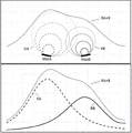
A schematic design of the composition of the compound coating subsets (30.1) - (30. n) and the transparent or translucent anti-reflection layer (40) is given in fig. 2.
Each co-sputtering process consists of a dual magnetron configuration containing a sputtering target a and a sputtering target B. The sputtering target a comprises material a (mata) and the sputtering target B comprises material B (matb). Each sputtering target is driven and controlled by a separate process power supply independent of the adjacent targets. The vapor flux from target a (va) is therefore different from the vapor flux from target b (vb). The two vapor fluxes (VA) and (VB) reach the substrate and mix to form a new coating. By adding reactive gases, e.g. nitrogen N2And/or oxygen O2Capable of reacting with the deposited coating to form a mixed compound coating. Due to the arrangement of the sputtering target and the tilt angle of the target orientation, the corresponding vapor flux may not be uniformly mixed. (RA + B) gives the overall distribution of deposition rate on the substrate surface. In this example, the vapor flow rate (VA) is 60% and the vapor flow rate (VB) is 40%. It is clear that the contribution of the vapor flux (VA) to the total distribution (RA + B) is higher. (RA) gives only the deposition rate distribution of the vapor flux (VA), and (RB) gives only the deposition rate distribution of the vapor flux (VB). In the material A (A composition gradient can be obtained in the mixture between MatA) and material b (matb), which provides more flexibility in the design of the compound coating. In this way, the average refractive index n and the extinction coefficient k of the compound coating can be adjusted. Further, the composition content gradient of the mixture can be adjusted by the arrangement of the sputtering target and the inclination angle of the orientation of the sputtering target.
By using the above method, the compound coating (30.1) - (30. N) and the translucent anti-reflection layer (40) can be designed such that each of these coatings is composed of a mixture of one material (MatA) and another material (MatB) which is partially to completely reactive with nitrogen N for the compound coating (30.1) - (30. N) and/or partially to completely reactive with oxygen for the translucent anti-reflection layer (40). The expression (MatA: MatB) Nx can be used for the compound coatings (30.1) - (30. N) or the expression (MatA: MatB) N can be used for the semitransparent antireflection layer (40)XOYIt is shown here that for compound coatings (30.1) - (30. N), if silicon or silicon-aluminum alloy is used as material a (mata) and chromium or chromium alloy is used as material b (matb) to create a compound coating (Si: Cr) Nx or (SiAl: Cr) Nx, and for transparent antireflection layer (40) (Si: Cr) NXOYOr (SiAl: Cr) NXOY。
The stainless steel substrate should be made of a stainless steel material of the grade having a chromium Cr content of not less than 10.5 at%. Preferably, austenitic stainless steel materials are used, such as commercial grades of 201, 304 or 316 stainless steel. Ferritic stainless steel materials, such as commercial grade 430 stainless steel, may also be used.
The stainless steel substrate further needs to be subjected to a surface treatment such as a mirror surface, such as commercial grade surface treatment BA or 8K. Or a matte surface such as commercial grade surface treatment 2B or 1B or a textured surface such as commercial grade wire H/L or No.4, but not limited to these surface treatments.
The stainless steel substrate can be a coiled strip or a plate. Wherein the base material thickness of the coil material strip can be 0.1mm to 1.5mm, and the width can be 100mm to 1500 mm; the substrate thickness of the panel may be 0.1mm to 4mm and the width may be 100mm to 1500 mm.
The sputtering target used for the co-sputtering process may contain alloying elements such as aluminum Al embedded in silicon Si to form a SiAl target. As long as chromium Cr or silicon Si is a determining element of the target, the present invention shall include the case of using chromium alloy and silicon alloy targets.
The coating of the adhesion layer (10), the metal nitride layer (20) and the semi-transparent anti-reflection layer (40) may be performed by using pulsed or non-pulsed direct current magnetron sputtering or bipolar or unipolar alternating current magnetron sputtering and/or electron beam evaporation or arc vapour deposition techniques.
The fully transparent antireflective layer (40) may be formed from silicon dioxide (SiO)2) Or silicon nitride (Si)3N4) The composition may be prepared by pulsed or non-pulsed direct current magnetron sputtering or bipolar or unipolar alternating current magnetron sputtering and/or electron beam evaporation.
The thickness of the adhesion layer (10) is between 20nm and 200nm, more preferably between 20nm and 60nm in typical applications. However, this part of the coating is not covered by the present invention, irrespective of the adhesion layer having a coating thickness below 20 nm.
The thickness of the optional metal nitride coating (20) may vary between 0nm (unplated) and 300nm, depending on its application.
The coating thickness of each compound coating (30.1) - (30. n) can vary from 5nm to 300nm, depending on the application.
The coating thickness of the optional transparent or translucent antireflection layer (40) may also vary from 5nm to 300nm, with the corresponding thickness depending on the application.
The CIELAB colour angle h ab can be achieved by adjusting the thickness of the individual compound coatings (30.1) - (30. n) and/or by adjusting their composition in order to achieve a value between 0 ° and 360 °. Composition of the (Si: Cr) mixture and degree of reaction with Nitrogen, NxCan be adjusted.
The CIE can also be adjusted by adjusting the thickness of the individual compound coatings (30.1) - (30. n) and/or by adjusting their compositionLAB color saturation, C ab (chroma, describing depth of color) and the brightness of the color described by the CIELAB L value. Composition of the (Si: Cr) mixture and degree of reaction with Nitrogen, NxCan be adjusted.
Thus, by adjusting the thickness and/or composition of the individual compound coatings (30.1) - (30. n), the CIELAB values can be adjusted over a wide range.
The thickness of the metal nitride layer (20) and the degree of reaction of the metal nitrites obtained by reaction with nitrogen, in particular chromium nitrides (CrN)x) The adjustment of CIELAB color values is facilitated.
An optional transparent or translucent anti-reflection coating on top of the compound coating helps to adjust the color saturation C or to make the color darker or lighter. The L value of CIELAB can be adjusted by adjusting the thickness of the transparent and/or translucent antireflective layer or by adjusting its composition. Here, it is possible not only to adjust the composition of the (Si: Cr) mixture and the degree of reaction N with nitrogenXThe degree of reaction O with oxygen can also be adjustedY。
The following are several specific examples of the present invention.
Example 1
Color: black color
Film system:
semitransparent antireflection layer: silicon aluminum chromium oxynitride (SiAl: Cr) NXOY
Thickness = 30nm
The content of silicon and aluminum (90%: 10%) is = 75%. 85%
Chromium content = 15%. 25%
x Nx = 0.25…0.35
y Oy = 0.65…0.75
Compound film layer 1: silicon aluminum chromium nitride (SiAl: Cr) Nx-1
Thickness = 35nm … 45nm
Silicon aluminum (90%: 10%) content = 60%. 70%
Chromium content = 30%. 40%
x NX = 1
A metal nitride film layer: 35nm … 45nm chromium nitride (CrNx)
An adhesion layer: 30nm chromium (Cr)
Base material: stainless steel, 430 alloy + BA mirror surface treatment.
CIELAB color values: l = 25, a =0, b = 0.
Pencil hardness scale: > 5H
Cross scratch adhesion test: grade 0 (without any stripping)
Neutral salt spray test performance:
cycle testing was continued for 10 consecutive days, 8 hours of salt spray and 16 hours of salt spray box standing.
No pitting occurred.
The color difference Δ Ε < 1.5, the color appearance was uniform.
Temperature and humidity environment test performance:
the test was carried out at 85 ℃, 85% r.h. relative humidity for 72 hours.
No pitting occurred.
The color difference Δ Ε < 1.5, the color appearance was uniform.
High temperature test performance:
baking for 72 hours at 180 ℃.
No corrosion spots occurred.
The color difference Δ Ε < 1.5, the color appearance was uniform.
Ultraviolet irradiation resistance:
no photocatalytically active material is used.
Example 2
Color: dark brown color
Film system:
semitransparent antireflection layer: silicon aluminum chromium oxynitride (SiAl: Cr) NXOY
Thickness = 35nm
The content of silicon and aluminum (90%: 10%) is = 75%. 85%
Chromium content = 15%. 25%
x Nx = 0.65…0.75
y Oy = 0.25…0.35
Compound film layer 1: silicon aluminum chromium nitride (SiAl: Cr) Nx-1
Thickness = 50nm … 70nm
Silicon aluminum (90%: 10%) content = 60%. 70%
Chromium content = 30%. 40%
x NX = 1
A metal nitride film layer: 35nm … 45nm chromium nitride (CrNx)
An adhesion layer: 30nm chromium (Cr)
Base material: stainless steel
CIELAB color values: l = 39.4, a = 0.3, b = 6.0.
Pencil hardness scale: > 5H
Cross scratch adhesion test: grade 0 (without any stripping)
Neutral salt spray test performance:
cycle testing was continued for 10 consecutive days, 8 hours of salt spray and 16 hours of salt spray box standing.
No corrosion spots occurred.
The color difference Δ Ε < 1.5, the color appearance was uniform.
Temperature and humidity environment test performance:
the test was carried out at 85 ℃, 85% r.h. relative humidity for 72 hours.
No corrosion spots occurred.
The color difference Δ Ε < 1.5, the color appearance was uniform.
High temperature test performance:
baking at 180 deg.C for 72 hr
No corrosion spots occurred.
The color difference Δ Ε < 1.5, the color appearance was uniform.
Ultraviolet irradiation resistance:
without using any photocatalytically active material
Example 3
Color: india blue
Film system:
semi-transparent antireflection layer: silicon aluminum chromium oxynitride (SiAl: Cr) NXOY
Thickness = 10nm
Silicon aluminum (90%: 10%) content = 70%. 80%
Chromium content = 20%. 30%
x Nx = 0.45…0.55
y Oy = 0.45…0.55
Compound film layer 1: silicon aluminum chromium nitride (SiAl: Cr) Nx-1
Thickness = 40nm … 60nm
Silicon aluminum (90%: 10%) content = 70%. 80%
Chromium content = 20%. 30%
x NX = 1
A metal nitride film layer: 35nm … 45nm chromium nitride (CrNx)
An adhesion layer: 30nm chromium (Cr)
Base material: stainless steel
CIELAB color values: l = 36.8, a = -2.7, b = -9.8.
Pencil hardness scale: > 5H
Cross scratch adhesion test: grade 0 (without any stripping)
Neutral salt spray test performance:
cycle testing was continued for 10 consecutive days, 8 hours of salt spray and 16 hours of salt spray box standing.
No corrosion spots occurred.
The color difference Δ Ε < 1.5, the color appearance was uniform.
Temperature and humidity environment test performance:
the test was carried out at 85 ℃, 85% r.h. relative humidity for 72 hours.
No corrosion spots occurred.
The color difference Δ Ε < 1.5, the color appearance was uniform.
High temperature test performance:
baking at 180 deg.C for 72 hr
No corrosion spots occurred.
The color difference Δ Ε < 1.5, the color appearance was uniform.
Ultraviolet irradiation resistance:
without using any photocatalytically active material
Example 4
Color: cold grey colour
Film system:
semitransparent antireflection layer: silicon aluminum chromium oxynitride (SiAl: Cr) NXOY
Thickness = 80nm
Silicon aluminium (90%: 10%) content = 45%. 65%
Chromium content = 35%. 55%
x Nx = 0.45…0.55
y Oy = 0.45…0.55
Compound film layer 1: silicon aluminum chromium nitride (SiAl: Cr) Nx-1
Thickness = 40nm … 60nm
Silicon aluminum (90%: 10%) content = 40%. 60%
Chromium content = 40%. 60%
x NX = 1
A metal nitride film layer: 35nm … 45nm chromium nitride (CrNx)
An adhesion layer: 30nm chromium (Cr)
Base material: stainless steel
CIELAB color values: l = 43.3, a = -0.1, b = -2.8.
Pencil hardness scale: > 5H
Cross scratch adhesion test: grade 0 (without any stripping)
Neutral salt spray test performance:
cycle testing was continued for 10 consecutive days, 8 hours of salt spray and 16 hours of salt spray box standing.
No corrosion spots occurred.
The color difference Δ Ε < 1.5, the color appearance was uniform.
Temperature and humidity environment test performance:
the test was carried out at 85 ℃, 85% r.h. relative humidity for 72 hours.
No corrosion spots occurred.
The color difference Δ Ε < 1.5, the color appearance was uniform.
High temperature test performance:
baking at 180 deg.C for 72 hr
No corrosion spots occurred.
The color difference Δ Ε < 1.5, the color appearance was uniform.
Ultraviolet irradiation resistance:
no photocatalytically active material is used.
Example 5
Color: coffee color
Film system:
semitransparent antireflection layer: silicon aluminum chromium oxynitride (SiAl: Cr) NXOY
Thickness = 40nm
Silicon aluminium (90%: 10%) content = 50%. 70%
Chromium content = 30%. 50%
x Nx = 0.20…0.40
y Oy = 0.60…0.80
Compound film layer 1: silicon aluminum chromium nitride (SiAl: Cr) Nx-1
Thickness = 70nm … 90nm
Silicon aluminum (90%: 10%) content = 20%. 40%
Chromium content = 60%. 80%
x NX = 1
A metal nitride film layer: 35nm … 45nm chromium nitride (CrNx)
An adhesion layer: 30nm chromium (Cr)
Base material: stainless steel
CIELAB color values: l × = 21.7, a × = 11.4, b × = 4.8.
Pencil hardness scale: > 5H
Cross scratch adhesion test: grade 0 (without any stripping)
Neutral salt spray test performance:
cycle testing was continued for 10 consecutive days, 8 hours of salt spray and 16 hours of salt spray box standing.
No rust spot generation
The color difference Δ Ε < 1.5, the color appearance was uniform.
Temperature and humidity environment test performance:
the test was carried out at 85 ℃, 85% r.h. relative humidity environment for 72 hours.
No corrosion spots occurred.
The color difference Δ Ε < 1.5, the color appearance was uniform.
High temperature test performance:
baking at 180 deg.C for 72 hr
No corrosion spots occurred.
The color difference Δ Ε < 1.5, the color appearance was uniform.
Ultraviolet irradiation resistance:
no photocatalytically active material is used.
The above description is only an embodiment of the present invention, but the design concept of the present invention is not limited thereto, and any insubstantial modifications made by using the design concept should fall within the scope of infringing the present invention.
Claims (9)
1. A decorative coating for a stainless steel substrate comprising at least one compound coating, said compound coating consisting of a silicon-chromium alloy partially to completely reacted with nitrogen N, each compound coating expressing the formula (Si: Cr) NXAll the compound coatings are plated on the film plating surface of the stainless steel base material by a physical vapor deposition method, and the method is characterized in that: plating a transparent or semitransparent antireflection layer on the compound coating, wherein the transparent or semitransparent antireflection layer is expressed by (Si: Cr) NXOYThe (Si: Cr) in the compound coating and the transparent or semitransparent antireflection layer is described as any ratio of 0-100% of silicon and chromium, an index X of an Nx subscript describes a reaction coefficient with nitrogen, and OYThe index Y of the subscript describes the reaction coefficient with oxygen, and the indexes X, Y all vary from 0 to 1; the silicon component of the transparent or semitransparent antireflection layer is obtained by sputtering and depositing a pure silicon target or a silicon alloy target, and the chromium component is obtained by sputtering and depositing a pure chromium target or a chromium alloy target.
2. The decorative coating of a stainless steel substrate according to claim 1, wherein: comprising a plurality of compound coatings, each containing a different composition, each compound coating being described using the expression (Si: Cr) Nx and constituting a sub-set film system comprising n compound coatings, n being an integer greater than 1, which describes the number of compound layers applied.
3. The decorative coating of a stainless steel substrate according to claim 1, wherein: the thickness of the transparent or semitransparent antireflection layer is 5-300 nm.
4. The decorative coating of a stainless steel substrate according to claim 1, wherein: an adhesion layer is plated between the film-coated surface of the stainless steel substrate and the first compound coating, and the adhesion layer is made of pure chromium.
5. The decorative coating of a stainless steel substrate according to claim 4, wherein: the thickness of the adhesion layer is 20-200 nm.
6. The decorative coating of a stainless steel substrate according to claim 4, wherein: a metal nitride layer is plated between the adhesion layer and the first compound coating, and the metal nitride layer is formed by chromium nitride CrN meeting the stoichiometric ratio or non-stoichiometric ratioxAnd (4) forming.
7. The decorative coating of a stainless steel substrate according to claim 1, wherein: a metal nitride layer is plated between the film-coated surface of the stainless steel substrate and the first compound coating, and the metal nitride layer is formed by chromium nitride CrN meeting the stoichiometric ratio or non-stoichiometric ratioxAnd (4) forming.
8. The decorative coating of a stainless steel substrate according to claim 6 or 7, wherein: the thickness of the metal nitride layer is 0-300 nm.
9. The decorative coating of a stainless steel substrate according to claim 1, wherein: the stainless steel substrate is composed of a stainless steel grade containing at least 10.5 at% chromium.
Priority Applications (1)
| Application Number | Priority Date | Filing Date | Title |
|---|---|---|---|
| CN202010542801.6A CN111663100B (en) | 2020-06-15 | 2020-06-15 | Decorative coating of stainless steel base material |
Applications Claiming Priority (1)
| Application Number | Priority Date | Filing Date | Title |
|---|---|---|---|
| CN202010542801.6A CN111663100B (en) | 2020-06-15 | 2020-06-15 | Decorative coating of stainless steel base material |
Publications (2)
| Publication Number | Publication Date |
|---|---|
| CN111663100A CN111663100A (en) | 2020-09-15 |
| CN111663100B true CN111663100B (en) | 2022-05-31 |
Family
ID=72387604
Family Applications (1)
| Application Number | Title | Priority Date | Filing Date |
|---|---|---|---|
| CN202010542801.6A Active CN111663100B (en) | 2020-06-15 | 2020-06-15 | Decorative coating of stainless steel base material |
Country Status (1)
| Country | Link |
|---|---|
| CN (1) | CN111663100B (en) |
Families Citing this family (3)
| Publication number | Priority date | Publication date | Assignee | Title |
|---|---|---|---|---|
| EP4101947A1 (en) * | 2021-06-10 | 2022-12-14 | Atotech Deutschland GmbH & Co. KG | Method for electrodepositing a dark chromium layer, substrate comprising same, and electroplating bath thereof |
| CN114540764B (en) * | 2022-02-28 | 2024-07-30 | 歌尔股份有限公司 | Film-coated product and preparation method thereof |
| CN114660691B (en) * | 2022-03-07 | 2025-11-21 | 福建新越金属材料科技有限公司 | Improved high-reflection mirror surface coating |
Citations (7)
| Publication number | Priority date | Publication date | Assignee | Title |
|---|---|---|---|---|
| JP2002277607A (en) * | 2001-03-21 | 2002-09-25 | Toppan Printing Co Ltd | Antireflection laminate and display device using the laminate |
| CN1898408A (en) * | 2003-12-23 | 2007-01-17 | 山特维克知识产权股份有限公司 | A stainless steel strip coated with a decorative layer |
| WO2009051595A1 (en) * | 2007-10-18 | 2009-04-23 | Midwest Research Institue | High temperature solar selective coatings |
| CN102534480A (en) * | 2010-12-23 | 2012-07-04 | 鸿富锦精密工业(深圳)有限公司 | Coating piece and preparation method thereof |
| CN107177824A (en) * | 2017-05-16 | 2017-09-19 | 福建新越金属材料科技有限公司 | The decorative coating prepared based on the common sputtering technology of magnetic control on stainless steel substrate |
| CN109341116A (en) * | 2018-09-17 | 2019-02-15 | 中国建筑材料科学研究总院有限公司 | A kind of Cr-Si-N-O solar energy selective absorption coating and preparation method thereof |
| WO2020040406A1 (en) * | 2018-08-24 | 2020-02-27 | (주)엘지하우시스 | Surface finishing material |
-
2020
- 2020-06-15 CN CN202010542801.6A patent/CN111663100B/en active Active
Patent Citations (7)
| Publication number | Priority date | Publication date | Assignee | Title |
|---|---|---|---|---|
| JP2002277607A (en) * | 2001-03-21 | 2002-09-25 | Toppan Printing Co Ltd | Antireflection laminate and display device using the laminate |
| CN1898408A (en) * | 2003-12-23 | 2007-01-17 | 山特维克知识产权股份有限公司 | A stainless steel strip coated with a decorative layer |
| WO2009051595A1 (en) * | 2007-10-18 | 2009-04-23 | Midwest Research Institue | High temperature solar selective coatings |
| CN102534480A (en) * | 2010-12-23 | 2012-07-04 | 鸿富锦精密工业(深圳)有限公司 | Coating piece and preparation method thereof |
| CN107177824A (en) * | 2017-05-16 | 2017-09-19 | 福建新越金属材料科技有限公司 | The decorative coating prepared based on the common sputtering technology of magnetic control on stainless steel substrate |
| WO2020040406A1 (en) * | 2018-08-24 | 2020-02-27 | (주)엘지하우시스 | Surface finishing material |
| CN109341116A (en) * | 2018-09-17 | 2019-02-15 | 中国建筑材料科学研究总院有限公司 | A kind of Cr-Si-N-O solar energy selective absorption coating and preparation method thereof |
Also Published As
| Publication number | Publication date |
|---|---|
| CN111663100A (en) | 2020-09-15 |
Similar Documents
| Publication | Publication Date | Title |
|---|---|---|
| CN111663100B (en) | Decorative coating of stainless steel base material | |
| US5427843A (en) | Ceramic-coated metal sheet | |
| EP0353060B1 (en) | Multi ceramic layer-coated metal plate and process for manufacturing same | |
| KR102033186B1 (en) | Tool with chromium-containing functional layer | |
| JP7484950B2 (en) | Coated object and method for producing same - Patent application | |
| CA3047901C (en) | Copper-based antimicrobial pvd coatings | |
| CN108239747B (en) | Mother-of-pearl substrate coated with yellow layer | |
| US20070275264A1 (en) | Stainless Steel Strip Coated With A Decorative Layer | |
| KR20070045269A (en) | Metal Products, Methods of Manufacturing Metal Products and Their Uses | |
| EP2829632B1 (en) | Golden rigid decorative member | |
| US11753332B2 (en) | Functional coated article | |
| CN107177824B (en) | Decorative coating prepared on stainless steel substrate based on magnetron co-sputtering technology | |
| CN113930721A (en) | Red copper golden PVD decorative film and preparation method thereof | |
| US20030072974A1 (en) | Decorative hard coating and method for manufacture | |
| US5192410A (en) | Process for manufacturing multi ceramic layer-coated metal plate | |
| CN107217231A (en) | The decorative coating prepared on aluminum substrates based on the common sputtering technology of magnetic control | |
| CN112458417A (en) | Growth process of multi-element layered hardened coating | |
| CN217895726U (en) | High-temperature oxidation-resistant coating for stainless steel substrate | |
| EP4640916A1 (en) | Coating for a substrate; substrate; and article | |
| CN113549872B (en) | black coating | |
| Teplin et al. | Combinatorial study of reactively sputtered Cr–Ti–N | |
| Li et al. | Al-Si-N hard coatings with tunable structural and optical properties via silicon content modulation | |
| KR20230096259A (en) | Metal color stainless steel sheet by using sputtering, and method for the same | |
| CA3208501A1 (en) | Coating system for plastic processing applications | |
| Wongtanasarasin et al. | Changes in structural, morphological, and corrosion properties of CrN thin film effected by varying N2 pressure in the sputtering process |
Legal Events
| Date | Code | Title | Description |
|---|---|---|---|
| PB01 | Publication | ||
| PB01 | Publication | ||
| SE01 | Entry into force of request for substantive examination | ||
| SE01 | Entry into force of request for substantive examination | ||
| GR01 | Patent grant | ||
| GR01 | Patent grant |