CN111490751B - On-chip resistor self-calibration circuit - Google Patents
On-chip resistor self-calibration circuit Download PDFInfo
- Publication number
- CN111490751B CN111490751B CN202010322253.6A CN202010322253A CN111490751B CN 111490751 B CN111490751 B CN 111490751B CN 202010322253 A CN202010322253 A CN 202010322253A CN 111490751 B CN111490751 B CN 111490751B
- Authority
- CN
- China
- Prior art keywords
- voltage
- chip resistor
- comparator
- resistor
- calibration circuit
- Prior art date
- Legal status (The legal status is an assumption and is not a legal conclusion. Google has not performed a legal analysis and makes no representation as to the accuracy of the status listed.)
- Active
Links
Images

Classifications
-
- H—ELECTRICITY
- H03—ELECTRONIC CIRCUITRY
- H03H—IMPEDANCE NETWORKS, e.g. RESONANT CIRCUITS; RESONATORS
- H03H11/00—Networks using active elements
- H03H11/02—Multiple-port networks
- H03H11/28—Impedance matching networks
Abstract
The invention discloses an on-chip resistor self-calibration circuit, which comprises a current-to-voltage module, a comparator and a finite state machine, wherein the current-to-voltage module comprises a first branch and a second branch, and an output voltage V is output between a current source I and a reference resistor in the first branch A Output voltage V between current source II and on-chip resistor array in second branch B The method comprises the steps of carrying out a first treatment on the surface of the The on-chip resistor array comprises n parallel resistor units, and each resistor unit comprises a resistor and a switch which are connected in series; said voltage V A And voltage V B Respectively transmitting to two input ends of the comparator, wherein the output end of the comparator is connected with the finite state machine, the finite state machine outputs a switch control signal according to the output result of the comparator, and the switch control signal controls the equivalent resistor R of the on-chip resistor array ray =R ext and/M. The on-chip resistor self-calibration circuit provided by the invention can avoid the interference of signal noise while ensuring the on-chip resistor precision, and can reduce the current consumption in the working process.
Description
Technical Field
The invention relates to the field of on-chip resistor calibration, in particular to an on-chip resistor self-calibration circuit.
Background
With the development of electronic information technology, the data volume required to be transmitted and processed is continuously increased; in particular, in the fields of video transmission, data storage, and the like, the amount of data to be transmitted is rapidly increasing with an increase in image resolution and storage space. Currently, the speed of commercial serial interfaces has reached the order of 10 Gbps. During the transmission process of the high-speed signal, the phenomena of reflection, crosstalk, standing waves and the like of the transmission signal can be caused due to the fact that the impedance is not matched, so that the signal quality is seriously affected, the signal integrity is damaged, and the receiving of a receiver is affected. Therefore, for the high-speed signal transmission circuit, a calibration circuit module is generally arranged to perform matching calibration on the output impedance of the transmitter so as to improve the signal transmission quality; the best matching impedance is generally defined as a range of 50Ω±10%.
The output stage of the existing terminal driving circuit is generally realized by MOS devices, the devices are influenced by PVT (Process, voltage and Temperature) fluctuation, the precision of the devices can reach +/-30%, and the precision of the on-chip resistor devices can only achieve +/-20%, so that a circuit structure capable of accurately calibrating the on-chip resistor is required to be searched.
Disclosure of Invention
The invention aims to provide an on-chip resistor self-calibration circuit which can ensure the on-chip resistor precision, avoid the interference of signal noise and reduce the current consumption in the working process.
In order to achieve the above purpose, the present invention adopts the following technical scheme: an on-chip resistor self-calibration circuit comprises a current-to-voltage module, a comparator and a finite state machine, wherein the current-to-voltage module comprises a first branch and a second branch, the first branch comprises a current source I and a reference resistor which are connected in series, and an output voltage V is output between the current source I and the reference resistor A The second branch comprises a current source II and an on-chip resistor array which are connected in series, and the output voltage V is between the current source II and the on-chip resistor array B The method comprises the steps of carrying out a first treatment on the surface of the The current value ratio of the current source I to the current source II is 1: m;
the on-chip resistor array comprises n parallel resistor units, each resistor unit comprises a resistor and a switch which are connected in series, and the n switches are controlled by switch signals respectively; n is an integer greater than 0;
said voltage V A And voltage V B Respectively transmitting to two input ends of the comparator, wherein the output end of the comparator is connected with the finite state machine, the finite state machine outputs a switch control signal according to the output result of the comparator, and the switch control signal controls the equivalent resistor R of the on-chip resistor array ray =R ext M; wherein R is ext Is the resistance value of the reference resistor.
Further, the voltage V A =I BIAS ×R ext Said voltage V B =I BIAS ×R ray X M; when the voltage V A Less than voltage V B When the comparator outputs a low level; when the voltage V A Greater than or equal to voltage V B When the comparator outputs high level, I BIAS Representing the bias current of current source i.
Further, when the self-calibration circuit is in a reset state, n switches in the on-chip resistor array are all turned off, and the voltage V A Less than voltage V B The comparator outputs a low level.
Further, after receiving the reset signal, the finite state machine enters a jump state; when the comparator outputs low level, the finite state machine outputs a switch control signal to control the switches in the on-chip resistor array to be sequentially closed, so that the equivalent resistance of the on-chip resistor array is gradually reduced; and until the comparator outputs high level, the finite state machine enters a locking state at the moment, and a switch control signal is acquired.
Further, the current source I is a first PMOS tube, the source electrode of the first PMOS tube is connected with a power supply, the drain electrode of the first PMOS tube is connected with one end of the reference resistor, the grid electrode of the first PMOS tube is connected with a bias voltage, and the other end of the reference resistor is grounded; the current source II is a second PMOS tube, the source electrode of the second PMOS tube is connected with a power supply, the drain electrode of the second PMOS tube is connected with one end of the on-chip resistor array, the grid electrode of the second PMOS tube is connected with bias voltage, and the other end of the on-chip resistor array is grounded.
Further, the current-to-voltage module further comprises an analog selection unit, wherein the output end of the analog selection unit outputs bias voltage or power supply voltage, and the bias voltage is smaller than the power supply voltage.
Further, the finite state machine outputs a power supply selection signal, which is input to the analog selection unit; when the finite state machine is in a jump state, the power supply selection signal controls the analog selection unit to output bias voltage; otherwise, the power supply selection signal controls the analog selection unit to output a power supply voltage.
Further, the comparator is a hysteresis comparator with a cross-coupled structure.
Further, the resistance values of n resistors in the on-chip resistor array are equal.
Further, the reference resistor is an external reference resistor.
The invention has the following beneficial effects: the analog selection unit can output two voltages, so that after self calibration is finished, the analog selection unit is switched to a low-power consumption mode, and current consumption in the working process of the circuit is reduced; the invention adopts a hysteresis comparator structure, so that the circuit has a certain noise margin, and the on-chip resistor array precision is ensured while the oscillation in a system comparison loop caused by switching noise is avoided.
Drawings
FIG. 1 is a schematic diagram of an on-chip resistor self-calibration circuit structure in accordance with the present invention;
FIG. 2 is a schematic diagram of an on-chip resistor array according to the present invention;
fig. 3 is a diagram of the operating states of the finite state machine in the self-calibration circuit.
Detailed Description
In order to make the objects, technical solutions and advantages of the present invention more apparent, the following detailed description of the specific embodiments of the present invention will be given with reference to the accompanying drawings.
As shown in figure 1, the on-chip resistor self-calibration circuit provided by the invention comprises a current-to-voltage module, a comparator and a finite state machine, wherein the current-to-voltage module comprises a first branch and a second branch, the first branch comprises a current source I and a reference resistor Rext which are connected in series, a node A is arranged between the current source I and the reference resistor Rext, and the voltage V is output at the node A A Preferably, the reference resistor is a reference resistor located outside the chip. The second branch comprises a current source II and an on-chip resistor array which are connected in series, a node B is arranged between the current source II and the on-chip resistor array, and the voltage V is output at the node B B The method comprises the steps of carrying out a first treatment on the surface of the The ratio of the current values of the current source I and the current source II canIn self-setting, for example, the current value of the current source i can be set in the present invention: current value of current source ii = 1: m, at this time, voltage V A =I BIAS ×R ext Voltage V B =I BIAS ×R ray ×M;R ext R is the resistance value of the reference resistor ray I is equivalent resistance of the on-chip resistor array BIAS Representing the bias current of current source i.
Referring to fig. 1, in the present invention, the current source i is a first PMOS transistor MB1, a source of the first PMOS transistor MB1 is connected to the power supply VDD, a drain of the first PMOS transistor MB is connected to one end of the reference resistor Rext, a gate of the first PMOS transistor is connected to the bias voltage Vbp, and the other end of the reference resistor Rext is grounded. The current source II is a second PMOS tube MB2, the source electrode of the second PMOS tube MB2 is connected with the power supply VDD, the drain electrode is connected with one end of the internal resistor array of the chip, the grid electrode is connected with the bias voltage Vbp, and the other end of the internal resistor array of the chip is grounded. The current-to-voltage module further comprises an analog selection unit, wherein the output end of the analog selection unit outputs bias voltage VBIAS or power supply voltage VDD, and the bias voltage VBIAS is smaller than the power supply voltage VDD. The output state of the analog selection unit in fig. 1 is controlled by the voltage control signal FINISH, and when the voltage control signal FINISH is 1, the analog selection unit outputs the power supply voltage VDD, and when the voltage control signal FINISH is 0, the analog selection unit outputs the bias voltage VBIAS. The correspondence between the value of the voltage control signal FINISH and the output value of the analog selection unit can be set at will, and only one correspondence is shown in fig. 1; and the following description is given by taking the example of fig. 1 as an example, and the working principle of the following description is also applicable to other corresponding relations.
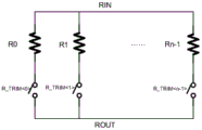
Referring to fig. 2, the on-chip resistor array of the present invention includes n parallel resistor units, where n is an integer greater than 0. Each resistor unit comprises a resistor and a switch which are connected in series, and n switches are respectively controlled by a switch control signal R_TRIM < n:0 >; the switch control signal R_TRIM < n:0> specifically includes n switch signals R_TRIM <0> to R_TRIM < n-1>, the switch signal R_TRIM < x > controls the switch connected with the resistor Rx, when R_TRIM < x > is 1, the switch is connected, and when R_TRIM < x > is 0, the switch is disconnected. The more the number of the switch signals R_TRIM < x > is 1 in the switch control signals R_TRIM < n:0>, the more the parallel resistors of the on-chip resistor array are turned on, and the smaller the equivalent resistance of the on-chip resistor array is. Preferably, the resistance values of n resistors in the on-chip resistor array in the present invention are equal.
It should be noted that the on-chip resistor array may also include resistors connected in parallel and/or resistors connected in series, and corresponding switch signals are added in the switch control signals; only the equivalent resistance of the on-chip resistor array needs to be adjustable.
With continued reference to FIG. 1, the voltage V of the present invention A And voltage V B The two inputs are respectively transmitted to the two inputs of the comparator, the voltage in fig. 1 is input to the non-inverting input of the comparator, and the voltage is input to the inverting input of the comparator, in practical application, the two inputs can be interchanged, and the principle is the same when the two inputs of the comparator are interchanged, which is described below by way of example only in fig. 1. Defining the output of the comparator as node C, voltage V A And voltage V B The comparison result V is obtained at the output end C of the comparator after comparison and amplification C When V A ≥V B When the voltage at the node C is higher than the voltage V at the output end of the comparator C Is VDD, when V A <V B When the comparator outputs a low level, the voltage V at the node C C Is 0.
As shown in fig. 1, the power consumption state of the comparator is controlled by the voltage control signal FINISH, when the voltage control signal FINISH is 1, the comparator enters a low power consumption state, and when the voltage control signal FINISH is 0, the comparator works normally.
The comparator in the invention preferably adopts a hysteresis comparator structure with a cross coupling structure. The hysteresis comparator has the advantages that the structure of the hysteresis comparator has certain hysteresis and has better immune effect on signal noise. Because the switch of the on-chip resistor array in the point-to-current voltage module can cause certain switch noise interference to appear at the output end of the comparator, in order to realize higher array control precision, each resistance value in the on-chip resistor array is smaller, so that the voltage change range of the node B is smaller each time, and the node B is more sensitive to the switch noise caused by the heavy switch of the on-chip resistor array. Therefore, a certain noise margin is required for the post comparator.
The output end of the comparator is connected with the finite state machine FSM, after the output result of the comparator is input into the finite state machine FSM, the finite state machine FSM outputs a switch control signal R_TRIM after the internal state machine jumps, and the jump regulation of the response is triggered<n:0>And a voltage control signal FINISH; when V is A ≥V B When the voltage value at the node C is VDD, the output end of the comparator outputs a high level, and the voltage control signal FINISH-1; when V is A <V B When the voltage at the node C is 0, the comparator output outputs a low level, and the voltage control signal finish=0.
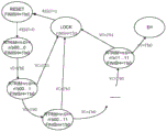
The working state diagram of the finite state machine is shown in a third diagram. When the finite state machine is in a jump state, the power supply selection signal controls the analog selection unit to output bias voltage; otherwise, the power supply selection signal controls the analog selection unit to output a power supply voltage. When the self-calibration circuit is in a reset state, n switches in the on-chip resistor array are all disconnected, and the voltage V A Less than voltage V B The comparator outputs a low level. After receiving the reset signal, the finite state machine enters a jump state; when the comparator outputs low level, the finite state machine outputs a switch control signal to control the on-chip resistor array switch to be sequentially closed, so that the equivalent resistance of the on-chip resistor array is gradually reduced; until the comparator outputs a high level, the finite state machine enters a locking state, and a switch control signal is acquired.
The state definition of the finite state machine FSM and the transitions between states are shown in fig. 3. The working principle is simpler, and the method can be realized by a linear shift register. It should be noted that the operating clock frequency of the finite state machine is preferably lower than a loop delay of the system to ensure that the decision and the jump of the system state are performed when the switch control signal change R_TRIM < n:0> at the previous time is reflected to the output voltage at the node C. Because the hysteresis comparator with the cross coupling structure is selected, the comparison process is faster than that of the comparators with other structures, thereby being beneficial to setting a higher loop bandwidth and reducing the time consumption of the self-calibration process of the resistor.
With continued reference to fig. 1, the on-chip resistor automatic calibration circuit of the present invention comprises the following steps: the circuit is initially in a reset state, the output R_TRIM of the FSM<n:0>All 0 and fish 0. At this time, the equivalent resistance of the on-chip resistor array is infinite, and the output voltage of the node B in the current-to-voltage module is the power supply voltage VDD. And the output voltage of the node A is the bias current I of the current source I BIAS And R is R ext Is a product of (a) and (b). At this time satisfy V A <V B Conditions of (2), then V C The output equivalent is the number 0.
After release of the RESET signal RESET, the finite state machine FSM starts state transitions. Due to V C Starting at 0, so FINSH output is 0, R_TRIM<n:0>One bit of the resistance array is changed into 1, the on-chip resistor array is connected with one path of resistor unit R0, and the equivalent resistance value R of the on-chip resistor array ray =r; wherein R is the resistance value of each resistor in the resistor unit. At this time, the voltage value at point B becomes I BIAS X M x R. At this time V A /V B If V is the voltage comparison result update of A Still smaller than V B V is then C Still 0, output R_TRIM of FSM<n:0>The on-chip resistor array is connected with two paths of resistor units R0 and R1 from one 1 to two 1, and the equivalent resistance value R of the on-chip resistor array is equal to the equivalent resistance value R of the on-chip resistor array ray After the equivalent resistance of the on-chip resistor array changes, the voltage value of the point B changes, the FSM state of the state machine is turned over, the FINISH is still 0, and the system repeats the previous steps until the parallel resistance of the on-chip resistor array is enough, so that the voltage V of the point A A Greater than or equal to the voltage V at the point B B At this point the C point output is 0 and the state machine jumps to the LOCK state, FINISH becomes 1. At this time, the self-calibration circuit completes the calibration operation to obtain the final array switch selection configuration R_TRIM<n:0>And storing the result in a system register until the next system reset to re-perform the resistance calibration. When the FINISH is 1, the voltage control signal FINISH controls the current-to-voltage module and the comparator to enter a low power consumption state, so that the calibration circuit does not cause extra power consumption under the normal working state of the system, and the purpose of low power consumption is realized.
In order to further reduce the current consumption in the working process, the resistance ranges of the reference resistor Rext and the on-chip resistor array can be defined by self. Meanwhile, the current proportion of two branches in the current-to-voltage module can be flexibly configured, and finally, the current can be locked to I BIAS ×R ex t=I BIAS ×M×R ray The equivalent value of the calibrated on-chip resistor array resistor is R ext and/M. And then the number of resistor strings or parallel connections in the resistor units is regulated in equal proportion, so that any accurate resistor value can be realized.
The foregoing description is only of the preferred embodiments of the present invention, and the embodiments are not intended to limit the scope of the invention, so that all changes made in the structure and details of the invention which may be regarded as equivalents thereof are intended to be included within the scope of the invention as defined in the following claims.
Claims (10)
1. The on-chip resistor self-calibration circuit is characterized by comprising a current-to-voltage module, a comparator and a finite state machine, wherein the current-to-voltage module comprises a first branch and a second branch, the first branch comprises a current source I and a reference resistor which are connected in series, and a voltage V is output between the current source I and the reference resistor A The second branch comprises a current source II and an on-chip resistor array which are connected in series, and the output voltage V is between the current source II and the on-chip resistor array B The method comprises the steps of carrying out a first treatment on the surface of the The current value ratio of the current source I to the current source II is 1: m;
the on-chip resistor array comprises n parallel resistor units, each resistor unit comprises a resistor and a switch which are connected in series, and the n switches are controlled by switch signals respectively; n is an integer greater than 0;
said voltage V A And voltage V B Respectively transmitting to two input ends of the comparator, wherein the output end of the comparator is connected with the finite state machine, the finite state machine outputs a switch control signal according to the output result of the comparator, and the switch control signal controls the equivalent resistor R of the on-chip resistor array ray =R ext M; wherein R is ext For referenceResistance value of the resistor.
2. An on-chip resistor self-calibration circuit according to claim 1, wherein said voltage V A =I BIAS ×R ext Said voltage V B =I BIAS ×R ray X M; when the voltage V A Less than voltage V B When the comparator outputs a low level; when the voltage V A Greater than or equal to voltage V B When the comparator outputs high level, I BIAS Representing the bias current of current source i.
3. The on-chip resistor self-calibration circuit according to claim 2, wherein n switches in said on-chip resistor array are all turned off when said self-calibration circuit is in a reset state, said voltage V A Less than voltage V B The comparator outputs a low level.
4. An on-chip resistor self-calibration circuit according to claim 3, wherein said finite state machine enters a skip state after receiving a reset signal; when the comparator outputs low level, the finite state machine outputs a switch control signal to control the switches in the on-chip resistor array to be sequentially closed, so that the equivalent resistance of the on-chip resistor array is gradually reduced; and until the comparator outputs high level, the finite state machine enters a locking state at the moment, and a switch control signal is acquired.
5. The on-chip resistor self-calibration circuit according to claim 1, wherein the current source I is a first PMOS tube, a source electrode of the first PMOS tube is connected with a power supply, a drain electrode of the first PMOS tube is connected with one end of the reference resistor, a grid electrode of the first PMOS tube is connected with a bias voltage, and the other end of the reference resistor is grounded; the current source II is a second PMOS tube, the source electrode of the second PMOS tube is connected with a power supply, the drain electrode of the second PMOS tube is connected with one end of the on-chip resistor array, the grid electrode of the second PMOS tube is connected with bias voltage, and the other end of the on-chip resistor array is grounded.
6. The on-chip resistor self-calibration circuit according to claim 1, wherein the current-to-voltage module further comprises an analog selection unit, an output terminal of the analog selection unit outputs a bias voltage or a power supply voltage, and the bias voltage is smaller than the power supply voltage.
7. The on-chip resistor self-calibration circuit according to claim 6, wherein said finite state machine outputs a power supply selection signal, said power supply selection signal being input to said analog selection unit; when the finite state machine is in a jump state, the power supply selection signal controls the analog selection unit to output bias voltage; otherwise, the power supply selection signal controls the analog selection unit to output a power supply voltage.
8. An on-chip resistor self-calibration circuit according to claim 1, wherein said comparator is a hysteretic comparator having a cross-coupled structure.
9. The on-chip resistor self-calibration circuit of claim 1, wherein n resistors in the on-chip resistor array have equal resistance values.
10. The on-chip resistor self-calibration circuit of claim 1, wherein the reference resistor is an external reference resistor.
Priority Applications (1)
| Application Number | Priority Date | Filing Date | Title |
|---|---|---|---|
| CN202010322253.6A CN111490751B (en) | 2020-04-22 | 2020-04-22 | On-chip resistor self-calibration circuit |
Applications Claiming Priority (1)
| Application Number | Priority Date | Filing Date | Title |
|---|---|---|---|
| CN202010322253.6A CN111490751B (en) | 2020-04-22 | 2020-04-22 | On-chip resistor self-calibration circuit |
Publications (2)
| Publication Number | Publication Date |
|---|---|
| CN111490751A CN111490751A (en) | 2020-08-04 |
| CN111490751B true CN111490751B (en) | 2023-05-12 |
Family
ID=71811093
Family Applications (1)
| Application Number | Title | Priority Date | Filing Date |
|---|---|---|---|
| CN202010322253.6A Active CN111490751B (en) | 2020-04-22 | 2020-04-22 | On-chip resistor self-calibration circuit |
Country Status (1)
| Country | Link |
|---|---|
| CN (1) | CN111490751B (en) |
Families Citing this family (4)
| Publication number | Priority date | Publication date | Assignee | Title |
|---|---|---|---|---|
| CN112596569B (en) * | 2020-12-17 | 2022-05-13 | 江苏科大亨芯半导体技术有限公司 | Circuit and method for calibrating internal resistance of photoelectric integrated chip |
| CN112650344B (en) * | 2020-12-22 | 2022-07-29 | 成都华微电子科技股份有限公司 | Configurable terminal matching resistance calibration circuit |
| CN112751565B (en) * | 2021-01-06 | 2024-02-09 | 北京遥测技术研究所 | Self-calibration on-chip reference voltage module |
| CN113253787A (en) | 2021-06-17 | 2021-08-13 | 苏州裕太微电子有限公司 | On-chip resistor correction circuit |
Citations (6)
| Publication number | Priority date | Publication date | Assignee | Title |
|---|---|---|---|---|
| US7161412B1 (en) * | 2005-06-15 | 2007-01-09 | National Semiconductor Corporation | Analog calibration of a current source array at low supply voltages |
| CN101505099A (en) * | 2002-11-14 | 2009-08-12 | 艾科嘉公司 | Switch power converter and system for controlling a plurality of the same |
| WO2014114004A1 (en) * | 2013-01-28 | 2014-07-31 | 香港中国模拟技术有限公司 | Self-calibration current source system |
| CN105119594A (en) * | 2015-07-30 | 2015-12-02 | 中国电子科技集团公司第五十八研究所 | High-speed serial port load automatic calibration circuit |
| CN109729295A (en) * | 2018-12-19 | 2019-05-07 | 芯原微电子(上海)有限公司 | Transmitting terminal driving circuit and method |
| CN111030630A (en) * | 2019-12-06 | 2020-04-17 | 深圳市纽瑞芯科技有限公司 | Circuit and method for calibrating on-chip RC time constant by using switched capacitor |
Family Cites Families (2)
| Publication number | Priority date | Publication date | Assignee | Title |
|---|---|---|---|---|
| US7915950B2 (en) * | 2008-06-20 | 2011-03-29 | Conexant Systems, Inc. | Method and algorithm of high precision on-chip global biasing using integrated resistor calibration circuits |
| US20160179113A1 (en) * | 2014-12-17 | 2016-06-23 | Sandisk Technologies Inc. | Temperature Independent Reference Current Generation For Calibration |
-
2020
- 2020-04-22 CN CN202010322253.6A patent/CN111490751B/en active Active
Patent Citations (6)
| Publication number | Priority date | Publication date | Assignee | Title |
|---|---|---|---|---|
| CN101505099A (en) * | 2002-11-14 | 2009-08-12 | 艾科嘉公司 | Switch power converter and system for controlling a plurality of the same |
| US7161412B1 (en) * | 2005-06-15 | 2007-01-09 | National Semiconductor Corporation | Analog calibration of a current source array at low supply voltages |
| WO2014114004A1 (en) * | 2013-01-28 | 2014-07-31 | 香港中国模拟技术有限公司 | Self-calibration current source system |
| CN105119594A (en) * | 2015-07-30 | 2015-12-02 | 中国电子科技集团公司第五十八研究所 | High-speed serial port load automatic calibration circuit |
| CN109729295A (en) * | 2018-12-19 | 2019-05-07 | 芯原微电子(上海)有限公司 | Transmitting terminal driving circuit and method |
| CN111030630A (en) * | 2019-12-06 | 2020-04-17 | 深圳市纽瑞芯科技有限公司 | Circuit and method for calibrating on-chip RC time constant by using switched capacitor |
Non-Patent Citations (1)
| Title |
|---|
| 高兴波 ; 赵毅强 ; 宋益伟 ; .一种带自动稳幅的新型电流模LC振荡器.微电子学与计算机.2012,(06),全文. * |
Also Published As
| Publication number | Publication date |
|---|---|
| CN111490751A (en) | 2020-08-04 |
Similar Documents
| Publication | Publication Date | Title |
|---|---|---|
| CN111490751B (en) | On-chip resistor self-calibration circuit | |
| KR101965788B1 (en) | Single-ended configurable multi-mode driver | |
| US10193552B1 (en) | Termination resistor calibration circuit and control method thereof | |
| US7786785B2 (en) | Peaking control circuit | |
| US7135884B1 (en) | Voltage mode transceiver having programmable voltage swing and external reference-based calibration | |
| US7382153B2 (en) | On-chip resistor calibration for line termination | |
| US6525558B2 (en) | Programmable impedance control circuit | |
| US20060087339A1 (en) | Impedance adjustment circuits and methods using replicas of variable impedance circuits | |
| US20020114146A1 (en) | Precision on-chip transmission line termination | |
| CN111999565B (en) | Capacitance measuring circuit | |
| CN102025358A (en) | MOS switching circuit with broadband and high linearity | |
| US6107867A (en) | Load termination sensing circuit | |
| CN111525966B (en) | Impedance calibration circuit applied to transmitter | |
| CN110572148A (en) | Driving circuit and operation method thereof | |
| CN112181043A (en) | Resistance calibration circuit and method for multiple ports | |
| CN112187214B (en) | IO impedance calibration circuit and method of FPGA | |
| US20180309448A1 (en) | Data transmission with power supply noise compensation | |
| US7477717B2 (en) | Input receiver circuit | |
| US7023258B2 (en) | Switch circuit | |
| US20050099219A1 (en) | Setting multiple chip parameters using one IC terminal | |
| KR101703121B1 (en) | Output driver with slew rate calibration | |
| US5514982A (en) | Low noise logic family | |
| US5646549A (en) | Semiconductor device having an output circuit for transmitting low-voltage differential signals | |
| CN1438764A (en) | Stable oscillator | |
| CN113839659B (en) | High-isolation single-pole double-throw switch circuit |
Legal Events
| Date | Code | Title | Description |
|---|---|---|---|
| PB01 | Publication | ||
| PB01 | Publication | ||
| SE01 | Entry into force of request for substantive examination | ||
| SE01 | Entry into force of request for substantive examination | ||
| GR01 | Patent grant | ||
| GR01 | Patent grant |