CN111263903A - Optical film and system including the same - Google Patents
Optical film and system including the same Download PDFInfo
- Publication number
- CN111263903A CN111263903A CN201880068287.8A CN201880068287A CN111263903A CN 111263903 A CN111263903 A CN 111263903A CN 201880068287 A CN201880068287 A CN 201880068287A CN 111263903 A CN111263903 A CN 111263903A
- Authority
- CN
- China
- Prior art keywords
- wavelengths
- optical filter
- selective layer
- article
- wavelength transmission
- Prior art date
- Legal status (The legal status is an assumption and is not a legal conclusion. Google has not performed a legal analysis and makes no representation as to the accuracy of the status listed.)
- Pending
Links
- 239000012788 optical film Substances 0.000 title description 2
- 230000003287 optical effect Effects 0.000 claims abstract description 148
- 230000005540 biological transmission Effects 0.000 claims abstract description 119
- 239000006096 absorbing agent Substances 0.000 claims abstract description 23
- 239000000049 pigment Substances 0.000 claims description 37
- 239000000975 dye Substances 0.000 claims description 33
- 239000012860 organic pigment Substances 0.000 claims description 7
- 239000000434 metal complex dye Substances 0.000 claims description 5
- 230000016776 visual perception Effects 0.000 claims description 5
- 239000001023 inorganic pigment Substances 0.000 claims description 3
- 239000000853 adhesive Substances 0.000 claims description 2
- 230000001070 adhesive effect Effects 0.000 claims description 2
- 239000010410 layer Substances 0.000 description 129
- 239000000758 substrate Substances 0.000 description 35
- 239000011248 coating agent Substances 0.000 description 16
- 238000000576 coating method Methods 0.000 description 16
- 238000000034 method Methods 0.000 description 14
- 239000000203 mixture Substances 0.000 description 14
- 239000000976 ink Substances 0.000 description 12
- 238000010586 diagram Methods 0.000 description 11
- 239000010408 film Substances 0.000 description 10
- 238000002834 transmittance Methods 0.000 description 10
- 229910052751 metal Inorganic materials 0.000 description 8
- 239000002184 metal Substances 0.000 description 8
- 238000010521 absorption reaction Methods 0.000 description 7
- 239000008393 encapsulating agent Substances 0.000 description 6
- 230000005670 electromagnetic radiation Effects 0.000 description 5
- 229920002799 BoPET Polymers 0.000 description 4
- 239000003086 colorant Substances 0.000 description 4
- 230000000694 effects Effects 0.000 description 4
- 239000011241 protective layer Substances 0.000 description 4
- -1 transition metal dithiols Chemical class 0.000 description 4
- YXFVVABEGXRONW-UHFFFAOYSA-N Toluene Chemical compound CC1=CC=CC=C1 YXFVVABEGXRONW-UHFFFAOYSA-N 0.000 description 3
- 230000008033 biological extinction Effects 0.000 description 3
- 239000011521 glass Substances 0.000 description 3
- 230000000873 masking effect Effects 0.000 description 3
- 239000002105 nanoparticle Substances 0.000 description 3
- 239000002245 particle Substances 0.000 description 3
- 125000002080 perylenyl group Chemical group C1(=CC=C2C=CC=C3C4=CC=CC5=CC=CC(C1=C23)=C45)* 0.000 description 3
- 239000000565 sealant Substances 0.000 description 3
- 229910052709 silver Inorganic materials 0.000 description 3
- 239000004332 silver Substances 0.000 description 3
- XEEYBQQBJWHFJM-UHFFFAOYSA-N Iron Chemical compound [Fe] XEEYBQQBJWHFJM-UHFFFAOYSA-N 0.000 description 2
- PXHVJJICTQNCMI-UHFFFAOYSA-N Nickel Chemical compound [Ni] PXHVJJICTQNCMI-UHFFFAOYSA-N 0.000 description 2
- SJEYSFABYSGQBG-UHFFFAOYSA-M Patent blue Chemical compound [Na+].C1=CC(N(CC)CC)=CC=C1C(C=1C(=CC(=CC=1)S([O-])(=O)=O)S([O-])(=O)=O)=C1C=CC(=[N+](CC)CC)C=C1 SJEYSFABYSGQBG-UHFFFAOYSA-M 0.000 description 2
- NRCMAYZCPIVABH-UHFFFAOYSA-N Quinacridone Chemical compound N1C2=CC=CC=C2C(=O)C2=C1C=C1C(=O)C3=CC=CC=C3NC1=C2 NRCMAYZCPIVABH-UHFFFAOYSA-N 0.000 description 2
- 239000000980 acid dye Substances 0.000 description 2
- 239000012790 adhesive layer Substances 0.000 description 2
- 150000004056 anthraquinones Chemical class 0.000 description 2
- 230000008901 benefit Effects 0.000 description 2
- 239000011230 binding agent Substances 0.000 description 2
- 150000001875 compounds Chemical class 0.000 description 2
- 230000001747 exhibiting effect Effects 0.000 description 2
- 238000003384 imaging method Methods 0.000 description 2
- 230000031700 light absorption Effects 0.000 description 2
- CSHWQDPOILHKBI-UHFFFAOYSA-N peryrene Natural products C1=CC(C2=CC=CC=3C2=C2C=CC=3)=C3C2=CC=CC3=C1 CSHWQDPOILHKBI-UHFFFAOYSA-N 0.000 description 2
- IEQIEDJGQAUEQZ-UHFFFAOYSA-N phthalocyanine Chemical compound N1C(N=C2C3=CC=CC=C3C(N=C3C4=CC=CC=C4C(=N4)N3)=N2)=C(C=CC=C2)C2=C1N=C1C2=CC=CC=C2C4=N1 IEQIEDJGQAUEQZ-UHFFFAOYSA-N 0.000 description 2
- 239000001007 phthalocyanine dye Substances 0.000 description 2
- 229920000139 polyethylene terephthalate Polymers 0.000 description 2
- 239000005020 polyethylene terephthalate Substances 0.000 description 2
- 230000008569 process Effects 0.000 description 2
- 230000002829 reductive effect Effects 0.000 description 2
- 239000002904 solvent Substances 0.000 description 2
- 229910052723 transition metal Inorganic materials 0.000 description 2
- IHWDSEPNZDYMNF-UHFFFAOYSA-N 1H-indol-2-amine Chemical compound C1=CC=C2NC(N)=CC2=C1 IHWDSEPNZDYMNF-UHFFFAOYSA-N 0.000 description 1
- DCYGAPKNVCQNOE-UHFFFAOYSA-N 2,2,2-triphenylacetic acid Chemical compound C=1C=CC=CC=1C(C=1C=CC=CC=1)(C(=O)O)C1=CC=CC=C1 DCYGAPKNVCQNOE-UHFFFAOYSA-N 0.000 description 1
- JVNKYYGQNQJOEN-UHFFFAOYSA-N 2-diazo-1h-naphthalen-1-ol Chemical class C1=CC=C2C(O)C(=[N+]=[N-])C=CC2=C1 JVNKYYGQNQJOEN-UHFFFAOYSA-N 0.000 description 1
- VYZAMTAEIAYCRO-UHFFFAOYSA-N Chromium Chemical compound [Cr] VYZAMTAEIAYCRO-UHFFFAOYSA-N 0.000 description 1
- 229930182559 Natural dye Natural products 0.000 description 1
- VYPSYNLAJGMNEJ-UHFFFAOYSA-N Silicium dioxide Chemical compound O=[Si]=O VYPSYNLAJGMNEJ-UHFFFAOYSA-N 0.000 description 1
- NINIDFKCEFEMDL-UHFFFAOYSA-N Sulfur Chemical compound [S] NINIDFKCEFEMDL-UHFFFAOYSA-N 0.000 description 1
- RTAQQCXQSZGOHL-UHFFFAOYSA-N Titanium Chemical compound [Ti] RTAQQCXQSZGOHL-UHFFFAOYSA-N 0.000 description 1
- AHWXCYJGJOLNFA-UHFFFAOYSA-N [1,4]benzoxazino[2,3-b]phenoxazine Chemical class O1C2=CC=CC=C2N=C2C1=CC1=NC3=CC=CC=C3OC1=C2 AHWXCYJGJOLNFA-UHFFFAOYSA-N 0.000 description 1
- 239000002253 acid Substances 0.000 description 1
- 150000007513 acids Chemical class 0.000 description 1
- 229910000272 alkali metal oxide Inorganic materials 0.000 description 1
- 150000004645 aluminates Chemical class 0.000 description 1
- 229940051880 analgesics and antipyretics pyrazolones Drugs 0.000 description 1
- 229910052787 antimony Inorganic materials 0.000 description 1
- WATWJIUSRGPENY-UHFFFAOYSA-N antimony atom Chemical compound [Sb] WATWJIUSRGPENY-UHFFFAOYSA-N 0.000 description 1
- 125000003118 aryl group Chemical group 0.000 description 1
- 125000000751 azo group Chemical group [*]N=N[*] 0.000 description 1
- 239000000981 basic dye Substances 0.000 description 1
- 230000015572 biosynthetic process Effects 0.000 description 1
- 229910052797 bismuth Inorganic materials 0.000 description 1
- JCXGWMGPZLAOME-UHFFFAOYSA-N bismuth atom Chemical compound [Bi] JCXGWMGPZLAOME-UHFFFAOYSA-N 0.000 description 1
- 230000000903 blocking effect Effects 0.000 description 1
- 230000000981 bystander Effects 0.000 description 1
- 229910052793 cadmium Inorganic materials 0.000 description 1
- BDOSMKKIYDKNTQ-UHFFFAOYSA-N cadmium atom Chemical compound [Cd] BDOSMKKIYDKNTQ-UHFFFAOYSA-N 0.000 description 1
- CJOBVZJTOIVNNF-UHFFFAOYSA-N cadmium sulfide Chemical compound [Cd]=S CJOBVZJTOIVNNF-UHFFFAOYSA-N 0.000 description 1
- CETPSERCERDGAM-UHFFFAOYSA-N ceric oxide Chemical compound O=[Ce]=O CETPSERCERDGAM-UHFFFAOYSA-N 0.000 description 1
- 229910000422 cerium(IV) oxide Inorganic materials 0.000 description 1
- 150000004770 chalcogenides Chemical class 0.000 description 1
- 239000003638 chemical reducing agent Substances 0.000 description 1
- 239000003795 chemical substances by application Substances 0.000 description 1
- ZCDOYSPFYFSLEW-UHFFFAOYSA-N chromate(2-) Chemical class [O-][Cr]([O-])(=O)=O ZCDOYSPFYFSLEW-UHFFFAOYSA-N 0.000 description 1
- 229910052804 chromium Inorganic materials 0.000 description 1
- 239000011651 chromium Substances 0.000 description 1
- 229910017052 cobalt Inorganic materials 0.000 description 1
- 239000010941 cobalt Substances 0.000 description 1
- GUTLYIVDDKVIGB-UHFFFAOYSA-N cobalt atom Chemical compound [Co] GUTLYIVDDKVIGB-UHFFFAOYSA-N 0.000 description 1
- 238000004891 communication Methods 0.000 description 1
- 239000002131 composite material Substances 0.000 description 1
- 238000009833 condensation Methods 0.000 description 1
- 230000005494 condensation Effects 0.000 description 1
- 239000000470 constituent Substances 0.000 description 1
- 230000008878 coupling Effects 0.000 description 1
- 238000010168 coupling process Methods 0.000 description 1
- 238000005859 coupling reaction Methods 0.000 description 1
- 125000000664 diazo group Chemical group [N-]=[N+]=[*] 0.000 description 1
- 239000000982 direct dye Substances 0.000 description 1
- 239000007884 disintegrant Substances 0.000 description 1
- 239000000986 disperse dye Substances 0.000 description 1
- 238000004049 embossing Methods 0.000 description 1
- 238000001914 filtration Methods 0.000 description 1
- 239000006081 fluorescent whitening agent Substances 0.000 description 1
- 239000000989 food dye Substances 0.000 description 1
- 125000000524 functional group Chemical group 0.000 description 1
- 150000004820 halides Chemical class 0.000 description 1
- 150000002466 imines Chemical class 0.000 description 1
- 238000007641 inkjet printing Methods 0.000 description 1
- 229910052742 iron Inorganic materials 0.000 description 1
- 230000001788 irregular Effects 0.000 description 1
- 239000004816 latex Substances 0.000 description 1
- 229920000126 latex Polymers 0.000 description 1
- 239000011254 layer-forming composition Substances 0.000 description 1
- 239000000991 leather dye Substances 0.000 description 1
- 230000000670 limiting effect Effects 0.000 description 1
- WPBNNNQJVZRUHP-UHFFFAOYSA-L manganese(2+);methyl n-[[2-(methoxycarbonylcarbamothioylamino)phenyl]carbamothioyl]carbamate;n-[2-(sulfidocarbothioylamino)ethyl]carbamodithioate Chemical compound [Mn+2].[S-]C(=S)NCCNC([S-])=S.COC(=O)NC(=S)NC1=CC=CC=C1NC(=S)NC(=O)OC WPBNNNQJVZRUHP-UHFFFAOYSA-L 0.000 description 1
- 238000004519 manufacturing process Methods 0.000 description 1
- 238000005259 measurement Methods 0.000 description 1
- NYGZLYXAPMMJTE-UHFFFAOYSA-M metanil yellow Chemical group [Na+].[O-]S(=O)(=O)C1=CC=CC(N=NC=2C=CC(NC=3C=CC=CC=3)=CC=2)=C1 NYGZLYXAPMMJTE-UHFFFAOYSA-M 0.000 description 1
- 229910003455 mixed metal oxide Inorganic materials 0.000 description 1
- 239000000983 mordant dye Substances 0.000 description 1
- CIPHTOQKGSLCLV-UHFFFAOYSA-N n-phenylnaphthalene-1-carboxamide Chemical class C=1C=CC2=CC=CC=C2C=1C(=O)NC1=CC=CC=C1 CIPHTOQKGSLCLV-UHFFFAOYSA-N 0.000 description 1
- 239000000978 natural dye Substances 0.000 description 1
- 229910052759 nickel Inorganic materials 0.000 description 1
- 239000013307 optical fiber Substances 0.000 description 1
- 125000002524 organometallic group Chemical group 0.000 description 1
- YRZZLAGRKZIJJI-UHFFFAOYSA-N oxyvanadium phthalocyanine Chemical compound [V+2]=O.C12=CC=CC=C2C(N=C2[N-]C(C3=CC=CC=C32)=N2)=NC1=NC([C]1C=CC=CC1=1)=NC=1N=C1[C]3C=CC=CC3=C2[N-]1 YRZZLAGRKZIJJI-UHFFFAOYSA-N 0.000 description 1
- 230000008447 perception Effects 0.000 description 1
- 229920000728 polyester Polymers 0.000 description 1
- 229920000642 polymer Polymers 0.000 description 1
- 229920000128 polypyrrole Polymers 0.000 description 1
- 238000007639 printing Methods 0.000 description 1
- 238000012545 processing Methods 0.000 description 1
- JEXVQSWXXUJEMA-UHFFFAOYSA-N pyrazol-3-one Chemical class O=C1C=CN=N1 JEXVQSWXXUJEMA-UHFFFAOYSA-N 0.000 description 1
- WVIICGIFSIBFOG-UHFFFAOYSA-N pyrylium Chemical compound C1=CC=[O+]C=C1 WVIICGIFSIBFOG-UHFFFAOYSA-N 0.000 description 1
- 150000004053 quinones Chemical class 0.000 description 1
- 239000000376 reactant Substances 0.000 description 1
- 239000000985 reactive dye Substances 0.000 description 1
- 230000009467 reduction Effects 0.000 description 1
- 230000004044 response Effects 0.000 description 1
- 150000003839 salts Chemical class 0.000 description 1
- 238000007650 screen-printing Methods 0.000 description 1
- 238000007764 slot die coating Methods 0.000 description 1
- 239000007779 soft material Substances 0.000 description 1
- 239000007787 solid Substances 0.000 description 1
- 239000000992 solvent dye Substances 0.000 description 1
- 230000003068 static effect Effects 0.000 description 1
- 239000011593 sulfur Substances 0.000 description 1
- 229910052717 sulfur Inorganic materials 0.000 description 1
- 239000000988 sulfur dye Substances 0.000 description 1
- 238000012360 testing method Methods 0.000 description 1
- OKYDCMQQLGECPI-UHFFFAOYSA-N thiopyrylium Chemical compound C1=CC=[S+]C=C1 OKYDCMQQLGECPI-UHFFFAOYSA-N 0.000 description 1
- 239000010936 titanium Substances 0.000 description 1
- 229910052719 titanium Inorganic materials 0.000 description 1
- 150000003624 transition metals Chemical class 0.000 description 1
- 238000000411 transmission spectrum Methods 0.000 description 1
- LSGOVYNHVSXFFJ-UHFFFAOYSA-N vanadate(3-) Chemical compound [O-][V]([O-])([O-])=O LSGOVYNHVSXFFJ-UHFFFAOYSA-N 0.000 description 1
- 229910052720 vanadium Inorganic materials 0.000 description 1
- GPPXJZIENCGNKB-UHFFFAOYSA-N vanadium Chemical compound [V]#[V] GPPXJZIENCGNKB-UHFFFAOYSA-N 0.000 description 1
- 239000000984 vat dye Substances 0.000 description 1
- 230000000007 visual effect Effects 0.000 description 1
- 229910000859 α-Fe Inorganic materials 0.000 description 1
Images


Classifications
-
- G—PHYSICS
- G02—OPTICS
- G02B—OPTICAL ELEMENTS, SYSTEMS OR APPARATUS
- G02B5/00—Optical elements other than lenses
- G02B5/20—Filters
- G02B5/22—Absorbing filters
- G02B5/223—Absorbing filters containing organic substances, e.g. dyes, inks or pigments
-
- G—PHYSICS
- G02—OPTICS
- G02B—OPTICAL ELEMENTS, SYSTEMS OR APPARATUS
- G02B5/00—Optical elements other than lenses
- G02B5/20—Filters
- G02B5/208—Filters for use with infrared or ultraviolet radiation, e.g. for separating visible light from infrared and/or ultraviolet radiation
-
- G—PHYSICS
- G02—OPTICS
- G02B—OPTICAL ELEMENTS, SYSTEMS OR APPARATUS
- G02B5/00—Optical elements other than lenses
- G02B5/20—Filters
- G02B5/26—Reflecting filters
Landscapes
- Physics & Mathematics (AREA)
- General Physics & Mathematics (AREA)
- Optics & Photonics (AREA)
- Health & Medical Sciences (AREA)
- Toxicology (AREA)
- Optical Filters (AREA)
Abstract
本发明公开了系统,该系统包括:光发射器或光接收器中的一者或两者或可检测对象;以及与光发射器或光接收器中的一者或两者相邻的光学滤光器,其中光学滤光器包括至少一个波长透射选择性层,该波长透射选择性层包括吸收体组分,其中波长透射选择性层至少部分地减少入射到该波长透射选择性层上的从701nm至849nm的波长的透射。

The present invention discloses a system comprising: one or both of a light transmitter or light receiver or a detectable object; and an optical filter adjacent to one or both of the light transmitter or light receiver Optical device, wherein the optical filter includes at least one wavelength transmission selective layer, the wavelength transmission selective layer includes an absorber component, wherein the wavelength transmission selective layer at least partially reduces incident on the wavelength transmission selective layer from Transmission of wavelengths from 701 nm to 849 nm.
Description
背景技术Background technique
光学滤光器可用于多种应用,该多种应用包括光通信系统、传感器、成像、科学和工业光学设备以及显示系统。光学滤光器通常包括管理入射电磁辐射(包括光)的透射的光学层。光学滤光器可反射或吸收入射光的一部分,并且透射入射光的另一部分。光学滤光器内的光学层可在波长选择性、光学透射率、光学透明度、光学雾度、折射率和各种其他属性方面有所不同。Optical filters can be used in a variety of applications including optical communication systems, sensors, imaging, scientific and industrial optics, and display systems. Optical filters typically include optical layers that manage the transmission of incident electromagnetic radiation, including light. Optical filters can reflect or absorb a portion of incident light and transmit another portion of incident light. Optical layers within optical filters can vary in wavelength selectivity, optical transmittance, optical transparency, optical haze, refractive index, and various other properties.
发明内容SUMMARY OF THE INVENTION
本文公开了波长透射选择性层,该波长透射选择性层至少部分地减少入射到该波长透射选择性层上的从701nm至849nm的波长的透射,该波长透射选择性层包括吸收体组分。Disclosed herein is a wavelength transmission selective layer that at least partially reduces transmission of wavelengths from 701 nm to 849 nm incident on the wavelength transmission selective layer, the wavelength transmission selective layer including an absorber component.
本文公开了系统,该系统包括光发射器或光接收器中的一者或两者;以及与该光发射器或光接收器中的一者或两者相邻的光学滤光器,其中该光学滤光器包括至少一个波长透射选择性层,该波长透射选择性层包括吸收体组分,其中该波长透射选择性层至少部分地减少入射到该波长透射选择性层上的从701nm至849nm的波长的透射。Disclosed herein is a system comprising one or both of an optical transmitter or optical receiver; and an optical filter adjacent to one or both of the optical transmitter or optical receiver, wherein the optical filter The optical filter includes at least one wavelength transmission selective layer, the wavelength transmission selective layer including an absorber component, wherein the wavelength transmission selective layer at least partially reduces from 701 nm to 849 nm incident on the wavelength transmission selective layer wavelength of transmission.
本文公开了包括光学滤光器的制品,其中该光学滤光器包括至少一个波长透射选择性层,该波长透射选择性层包括吸收体组分,其中该波长透射选择性层至少部分地减少入射到该波长透射选择性层上的从701nm至849nm的波长的透射。Disclosed herein are articles comprising an optical filter, wherein the optical filter comprises at least one wavelength transmission selective layer, the wavelength transmission selective layer comprises an absorber component, wherein the wavelength transmission selective layer at least partially reduces incidence Transmission of wavelengths from 701 nm to 849 nm onto the wavelength transmission selective layer.
上述发明内容并不旨在描述本公开的每种实施方案。本公开的一个或多个实施方案的细节也阐述在以下说明中。依据说明书并且依据权利要求书,本公开的其他特征、目标和优点将显而易见。The above summary is not intended to describe every embodiment of the present disclosure. The details of one or more embodiments of the disclosure are also set forth in the description below. Other features, objects, and advantages of the present disclosure will be apparent from the description and from the claims.
附图说明Description of drawings
结合附图考虑本发明各种实施方案的下列详细描述将可以更完整地理解本发明,其中:The invention will be more fully understood from the following detailed description of various embodiments of the invention when considered in conjunction with the accompanying drawings, in which:
图1A至图1E示出了包括在本发明公开的光学制品中的回射元件的各种图案。1A-1E illustrate various patterns of retroreflective elements included in the disclosed optical articles.
图2A至图2E为包括光学滤光器的示例性光学系统的概念图和示意图。2A-2E are conceptual and schematic diagrams of exemplary optical systems including optical filters.
图3A至图3D为示例性系统的概念图,该示例性系统包括示例性光学滤光器以及显示可视觉感知图案和不可见近红外图案的电子显示器。3A-3D are conceptual diagrams of an exemplary system including an exemplary optical filter and an electronic display displaying a visually perceptible pattern and an invisible near-infrared pattern.
图4为示例性技术的流程图。4 is a flow diagram of an exemplary technique.
应当理解,在不脱离本发明范围的前提下,可利用实施方案并修改其结构。图未必按照比例绘制。图中使用的相似数字指代相似的部件。然而,应当理解,在给定图中使用数字指代部件不旨在限制另一图中用相同数字标记的部件。It is to be understood that the embodiments may be utilized and the structure thereof modified without departing from the scope of the present invention. Figures are not necessarily drawn to scale. Like numbers used in the figures refer to like parts. It should be understood, however, that the use of numerals to refer to components in a given figure is not intended to limit components marked with the same numerals in another figure.
具体实施方式Detailed ways
在本公开中,“紫外”是指介于约10nm和约400nm之间的范围内的波长。在本公开中,“可见”是指介于约400nm和约700nm之间的范围内的波长,并且“近红外”是指介于约700nm和约2000nm之间的范围内的波长,例如介于约800nm和约1200nm之间的范围内的波长。In this disclosure, "ultraviolet" refers to wavelengths in the range between about 10 nm and about 400 nm. In the present disclosure, "visible" refers to wavelengths in the range between about 400 nm and about 700 nm, and "near infrared" refers to wavelengths in the range between about 700 nm and about 2000 nm, eg, between about 800 nm and wavelengths in the range between about 1200nm.
电磁辐射的环境源可干扰被配置为接收特定波长的光或来自特定源的光的接收器,或者干扰被配置为发射特定波长的光的光发射器。例如,可见光波长可例如通过增加光接收器或光发射器中的噪声来干扰接收、感测或透射近红外波长。电磁辐射的源也可无意中暴露给旁观者(例如,在可见光范围内观看的人类观察者)。例如,虽然被配置为仅发射近红外波长的光发射器所发射的光可能无法被视觉感知,但负责发射光的装置或结构例如光发射器的外壳可被视觉感知。遮蔽、隐蔽或以其他方式掩蔽光发射器可能存在挑战,因为掩蔽技术可能不期望地导致所需的近红外波长在透射中受到阻挡、干扰或减少。Ambient sources of electromagnetic radiation can interfere with receivers configured to receive specific wavelengths of light or light from specific sources, or interfere with optical transmitters configured to emit specific wavelengths of light. For example, visible light wavelengths may interfere with receiving, sensing, or transmitting near infrared wavelengths, such as by increasing noise in the light receiver or light transmitter. Sources of electromagnetic radiation can also be inadvertently exposed to bystanders (eg, human observers viewing in the visible range). For example, while light emitted by a light emitter configured to emit only near infrared wavelengths may not be visually perceptible, the device or structure responsible for emitting the light, such as the housing of the light emitter, may be visually perceptible. Shading, concealing, or otherwise masking light emitters can present challenges because masking techniques can undesirably cause desired near-infrared wavelengths to be blocked, interfered with, or reduced in transmission.
根据本公开的实施例的光学滤光器可用于防止来自特定波长的不想要的光学干涉,或者用于掩蔽电磁辐射源使其不被可见感知,同时至少部分地允许所需的近红外波长由光发射器透射或由光接收器接收,或者同时允许以相对高的透明度透射近红外波长。例如,用于接收或感测近红外波长的光接收器可被屏蔽可见光波长,从而防止可由可见光波长引起的对近红外波长的接收或感测的干扰。用于透射近红外波长的光发射器可通过散射可见光波长而被掩蔽从而不被可见感知。例如,散射的可见光波长可隐蔽光发射器的存在,而不妨碍近红外波长的透射。Optical filters according to embodiments of the present disclosure may be used to prevent unwanted optical interference from certain wavelengths, or to mask a source of electromagnetic radiation from being visibly perceived, while at least partially allowing desired near-infrared wavelengths from The light transmitter transmits or is received by the light receiver, or at the same time allows transmission of near infrared wavelengths with relatively high transparency. For example, a light receiver for receiving or sensing near-infrared wavelengths may be shielded from visible light wavelengths, thereby preventing interference with the reception or sensing of near-infrared wavelengths that may be caused by visible light wavelengths. Light emitters used to transmit near infrared wavelengths can be masked from visible perception by scattering visible wavelengths. For example, scattered visible wavelengths can obscure the presence of light emitters without hindering the transmission of near infrared wavelengths.
本发明所公开的系统可包括:光接收器和光发射器中的一者或两者,以及包括波长透射选择性层的光学滤光器,该波长透射选择性层可至少部分地减少从701nm至849nm的波长的透射,同时至少部分地允许其他波长的透射。例如,该波长透射选择性层可散射大部分入射可见光。The disclosed systems can include one or both of a light receiver and a light transmitter, and an optical filter including a wavelength transmission selective layer that can at least partially reduce from 701 nm to Transmission of a wavelength of 849 nm, while at least partially allowing transmission of other wavelengths. For example, the wavelength transmission selective layer can scatter a majority of incident visible light.
在一些实施方案中,至少部分地减少从701nm至849nm的波长的透射的层透射少于约50%的从中穿过的从701nm至849nm的入射波长,在一些实施方案中透射少于约40%的从中穿过的从701nm至849nm的入射波长,在一些实施方案中透射少于约30%的从中穿过的从701nm至849nm的入射波长,在一些实施方案中透射少于约20%的从中穿过的从701nm至849nm的入射波长,或者在一些实施方案中透射少于约15%的从中穿过的从701nm至849nm的入射波长。在一些实施方案中,至少部分地减少从701nm至849nm的波长的透射的层阻挡至少20%的从400nm至700nm的波长,在一些实施方案中阻挡至少50%的从400nm至700nm的波长,在一些实施方案中阻挡至少80%的从400nm至700nm的波长,在一些实施方案中阻挡约100%的从400nm至700nm的波长,其中被阻挡的波长由该层吸收或反射。In some embodiments, the layer that at least partially reduces transmission of wavelengths from 701 nm to 849 nm transmits less than about 50%, and in some embodiments transmits less than about 40%, of incident wavelengths from 701 nm to 849 nm therethrough of incident wavelengths from 701 nm to 849 nm passing therethrough, in some embodiments less than about 30% of the incident wavelengths passing therethrough from 701 nm to 849 nm, in some embodiments less than about 20% of the incident wavelengths passing therethrough Incident wavelengths from 701 nm to 849 nm that pass therethrough, or in some embodiments less than about 15% of the incident wavelengths from 701 nm to 849 nm that pass therethrough. In some embodiments, the layer that at least partially reduces transmission of wavelengths from 701 nm to 849 nm blocks at least 20% of wavelengths from 400 nm to 700 nm, and in some embodiments blocks at least 50% of wavelengths from 400 nm to 700 nm, in In some embodiments at least 80% of wavelengths from 400 nm to 700 nm are blocked, in some embodiments about 100% of wavelengths from 400 nm to 700 nm are blocked, wherein the blocked wavelengths are absorbed or reflected by the layer.
本发明所公开的波长透射选择性层可包括吸收体组分。波长透射选择性粘合剂层在最终组件或制品中可以是平面的、非平面的或两者都可以。波长选择性层可定位在二维表面、三维表面或这两类表面的组合上。波长透射选择性层也可使用包括压印、拉伸、模内加工、相似类型的工艺或它们的组合的技术在形成后进行修改。The wavelength transmission selective layers disclosed herein may include an absorber component. The wavelength transmissive selective adhesive layer may be planar, non-planar, or both in the final assembly or article. The wavelength selective layer can be positioned on a two-dimensional surface, a three-dimensional surface, or a combination of both types of surfaces. The wavelength transmission selective layer may also be modified after formation using techniques including embossing, stretching, in-mold processing, similar types of processes, or combinations thereof.
吸收体组分可包括一种或多种染料、一种或多种颜料,或它们的组合。可用的吸收体组分可包括可至少部分地减少从701nm至849nm的波长的透射、同时至少部分地允许其他波长的透射的任何染料、颜料或它们的组合。The absorber component may include one or more dyes, one or more pigments, or a combination thereof. Useful absorber components can include any dye, pigment, or combination thereof that can at least partially reduce transmission of wavelengths from 701 nm to 849 nm, while at least partially allowing transmission of other wavelengths.
可用的吸收体组分包括在溶剂涂覆的组合物的情况下可溶于溶剂的那些组分。可用的吸收体组分也可包括不引起显著的近红外散射的那些组分。Useful absorber components include those components that are solvent-soluble in the case of solvent-coated compositions. Useful absorber components may also include those components that do not cause significant near-infrared scattering.
可用作本发明所公开的波长透射选择性层中的吸收体组分的例示性染料和颜料可包括那些视觉上呈现黑色或有颜色的但对近红外波长透明的组分。可见染料和着色剂属于一种或多种类别,如酸性染料、偶氮着色剂耦合组分以及重氮组分。碱性染料包括显色剂、直接染料、分散染料、荧光增白剂、食品染料、显色染料、皮革染料、媒染染料、天然染料和颜料、氧化碱、颜料、活性染料、还原剂、溶剂染料、硫化染料、缩硫染料、还原染料。染料也可基于主要负责光学吸收的官能团或部分进行分类。主要类别的染料/颜料中的一些包括酞菁、花青、过渡金属二噻醇、方酸、克酮酸、醌、蒽醌、亚胺、吡喃鎓、噻喃鎓、薁鎓、偶氮、苝和吲哚胺。这些染料和颜料中的许多本质上是有机/有机金属或金属有机的。这些染料中的一些可以是金属络合物。一组具体的金属络合物染料以商品名


吸收体组分在用于形成波长透射选择性层的组合物或溶液中的量可取决于许多因素,这些因素包括例如该层将形成的厚度、特定的吸收体组分、其他因素以及它们的组合。在利用染料的一些实施方案中,形成该波长透射选择性层的组合物涂覆得相对厚(例如,约2密耳(约0.051mm)),使得可利用相对少量的染料。在一些实施方案中,可利用基于组合物的总重量计具有不少于0.1重量%、不少于0.2重量%或不少于0.5重量%的染料的组合物。在一些实施方案中,可利用基于组合物的总重量计具有不多于10重量%、不少于5重量%或不少于2重量%的染料的组合物。The amount of the absorber component in the composition or solution used to form the wavelength transmission selective layer can depend on a number of factors including, for example, the thickness of the layer to be formed, the particular absorber component, other factors, and their combination. In some embodiments utilizing dyes, the composition forming the wavelength transmission selective layer is applied relatively thick (eg, about 2 mils (about 0.051 mm)) so that relatively small amounts of dye can be utilized. In some embodiments, compositions having no less than 0.1 wt %, no less than 0.2 wt %, or no less than 0.5 wt % dye based on the total weight of the composition can be utilized. In some embodiments, compositions having no more than 10 wt %, no less than 5 wt %, or no less than 2 wt % dye based on the total weight of the composition can be utilized.
如果颜料可充分分散在粘合剂中而不引起显著的近红外散射、不具有显著的近红外吸收或它们的组合,则该颜料也可为可用的吸收体组分。在一些实施方案中,可以纳米粒子形式利用可用的颜料。有机颜料和无机颜料两者均可被利用。在一些实施方案中,可用的有机颜料可包括通常在可商购获得的油墨中利用的一些颜料。可利用的具体例示性有机颜料可包括例如有机喹吖啶酮颜料,


染料也可以是可用的吸收体组分。不同的染料具有不同的吸收系数,但另一方面,颜料同时表现出吸收和散射两者,因此颜料的光学属性由消光系数来描述。颜料的粒度对其散射行为具有强烈的影响。粒度在纳米尺寸范围内的颜料显示出相对显著减少的散射。可使用此类光学特性来确定染料或颜料(或组合)在形成层或层自身的组合物中的量。对于给定的涂层厚度,染料或颜料的载量与它们的吸收/消光系数成反比。对于给定的透射率,颜料/染料的载量或浓度取决于该层的厚度和消光/吸收系数。如果吸收系数已知,则可使用比尔-朗伯定律计算给定透射率所需的浓度。该定律在稀溶液中效果很好,但由于散射、荧光等原因,该定律在较高浓度下可能会存在限制。Dyes can also be useful absorber components. Different dyes have different absorption coefficients, but on the other hand, pigments exhibit both absorption and scattering, so the optical properties of pigments are described by the extinction coefficient. The particle size of a pigment has a strong influence on its scattering behavior. Pigments with particle sizes in the nanometer size range show relatively significantly reduced scattering. Such optical properties can be used to determine the amount of dye or pigment (or combination) in the composition forming the layer or the layer itself. For a given coating thickness, the loading of dyes or pigments is inversely proportional to their absorption/extinction coefficients. For a given transmittance, the loading or concentration of pigment/dye depends on the thickness and extinction/absorption coefficient of the layer. If the absorption coefficient is known, the Beer-Lambert law can be used to calculate the concentration required for a given transmittance. This law works well in dilute solutions, but may have limitations at higher concentrations due to scattering, fluorescence, etc.
在一些实施方案中,形成波长透射选择性层的组合物可被分配在基底上(例如,印刷在基底上等)。印刷可使用如丝网印刷、槽模涂覆,甚至喷墨印刷的此类工艺来完成。可通过将组合物施加或分配到基底上来形成波长透射选择性层。例示性可用的基底可包括各种类型的基底,这些基底部分地取决于待形成的波长透射选择性层的期望用途。在一些实施方案中,可用的基底可包括聚酯,诸如聚对苯二甲酸乙二醇酯(PET)。In some embodiments, the wavelength transmission selective layer-forming composition can be dispensed on a substrate (eg, printed on a substrate, etc.). Printing can be done using such processes as screen printing, slot die coating, or even ink jet printing. The wavelength transmission selective layer can be formed by applying or dispensing the composition onto a substrate. Exemplary useful substrates can include various types of substrates, depending in part on the desired use of the wavelength transmission selective layer to be formed. In some embodiments, useful substrates may include polyesters such as polyethylene terephthalate (PET).
在一些实施方案中,波长透射选择性层至少部分地允许从701nm至849nm的波长的透射。在一些实施方案中,波长透射选择性层至少部分地减少从701nm至849nm的波长的透射,并且至少部分地减少从350nm至700nm的波长的透射,使得该波长透射选择性层至少部分地减少从350nm到849nm的波长的透射。In some embodiments, the wavelength transmission selective layer at least partially allows transmission of wavelengths from 701 nm to 849 nm. In some embodiments, the wavelength transmission selective layer at least partially reduces transmission of wavelengths from 701 nm to 849 nm, and at least partially reduces transmission of wavelengths from 350 nm to 700 nm, such that the wavelength transmission selective layer at least partially reduces transmission from wavelengths from 350 nm to 700 nm. Transmission of wavelengths from 350 nm to 849 nm.
在一些实施方案中,波长透射选择性层使从701nm至849nm的波长的透射减少至少50%、至少40%、至少30%、至少20%或至少15%。在一些实施方案中,波长透射选择性层不需要使从701nm至849nm的所有波长减少相同的量,并且百分比减少由光谱仪测量为穿过波长透射选择性层的光的从701nm至849nm的波长与穿过不具有吸收体组分的波长透射选择性层的光的从701nm至849nm的波长之比。In some embodiments, the wavelength transmission selective layer reduces transmission of wavelengths from 701 nm to 849 nm by at least 50%, at least 40%, at least 30%, at least 20%, or at least 15%. In some embodiments, the wavelength transmission selective layer need not reduce all wavelengths from 701 nm to 849 nm by the same amount, and the percentage reduction measured by the spectrometer as wavelengths from 701 nm to 849 nm of light passing through the wavelength transmission selective layer is the same as The ratio of wavelengths from 701 nm to 849 nm of light passing through a wavelength transmission selective layer without an absorber component.
在一些实施方案中,波长透射选择性层可由多于一个层制成或包括多于一个层,例如,该波长透射选择性层可以是多层膜或结构。在一些情况下,多层膜因为易于处理和施加而可以是有利的。例如,较硬的弹性层与较软的更粘稠的层组合可有利于将制品转化成模切,或者当柔软的更粘稠的层与三维特征部(诸如油墨梯级)相邻定位时,该组合可允许更容易地覆盖此类三维特征部。也可有利地利用多层膜以更容易地修改该膜的光密度(例如,对于层的给定总厚度,可利用透光层来减少位于透明层上方或下方的另一个层的光密度);或该膜的可见外观(例如,一层可以是绿色,而第二层可以是蓝色,以提供具有这两种颜色的复合色的外观)。In some embodiments, the wavelength transmission selective layer may be made of or include more than one layer, eg, the wavelength transmission selective layer may be a multilayer film or structure. In some cases, multilayer films can be advantageous for ease of handling and application. For example, a harder elastic layer in combination with a softer, more viscous layer may facilitate converting an article to die cut, or when a softer, more viscous layer is positioned adjacent to a three-dimensional feature such as an ink step, This combination may allow for easier covering of such three-dimensional features. Multilayer films can also be advantageously utilized to more easily modify the optical density of the film (eg, for a given total thickness of a layer, a light transmissive layer can be utilized to reduce the optical density of another layer above or below the transparent layer) ; or the visible appearance of the film (eg, one layer can be green and the second layer can be blue to provide the appearance of a composite color of the two colors).
波长透射选择性层也可与一个或多个可检测的对象相邻地使用。可检测的对象可以是例如反射近红外波长的对象。在一些实施方案中,可检测的对象可以是回射器,该回射器响应于照射在其上的光的一个或多个波长而反射(或以其他方式)近红外波长。A wavelength transmission selective layer can also be used adjacent to one or more detectable objects. A detectable object may be, for example, an object that reflects near infrared wavelengths. In some embodiments, the detectable object may be a retroreflector that reflects (or otherwise) near infrared wavelengths in response to one or more wavelengths of light impinging thereon.
波长透射选择性层可靠近光学制品中的任何部件使用。此类光学制品可称为光学滤光器。图1A-图1E为包括光学滤光器的示例性制品的横向剖视图。The wavelength transmission selective layer can be used adjacent to any component in the optical article. Such optical articles may be referred to as optical filters. 1A-1E are lateral cross-sectional views of exemplary articles including optical filters.
图1A示出了示例性制品10a的横向剖视图。制品10a包括基底12和波长透射选择性层14。基底12可包括玻璃、聚合物、金属或任何其他合适的刚性材料、半刚性材料或软材料以及它们的组合。虽然基底12被示为图1A中的示例性制品10a中的层,但在示例中,基底12可呈现可具有平坦表面、基本上平坦表面或纹理化表面的任何合适的三维形状。在示例中,基底12可包括外壳、屏幕或器件(例如,电子器件)的表面。FIG. 1A shows a transverse cross-sectional view of an
波长透射选择性层14至少部分地减少从701nm至849nm的波长的透射。在示例中,波长透射选择性层14可透射少于约50%的从701nm至849nm的波长。在示例中,波长透射选择性层14可透射少于约50%的从701nm至849nm的波长,并且透射少于约50%的低于700nm的波长。在示例中,波长透射选择性层14可散射多于约50%的低于700nm的波长。例如,波长透射选择性层14可通过散射超过约50%的低于700nm的入射波长来透射少于约50%的低于700nm的入射波长。The wavelength transmission
图1B示出了示例性制品10b的横向剖视图。制品10b可包括基底12、波长透射选择性层14以及反射层16。虽然在制品10b中的波长透射选择性层14与基底12之间示出了反射层16,但在示例中,制品10b可不包括基底12,并且该波长透射选择性层可设置在反射层16上。在示例中,基底12可包括例如在基底12的主表面处或内部内的反射层16。在示例中,反射层16可设置在基底12下方。在示例中,反射层16可设置在基底12上方。在示例中,反射层16可以是穿孔的。在示例中,制品10b可反射少于50%的可见光,并且透射超过50%的近红外光。在示例中,反射层16可以是波长选择性的,例如仅反射选定波长。反射层16可包括多层光学膜、二向色性反射器、干涉膜、无机多层叠堆、金属电介质叠堆、抛光基底、反射镜、反射偏振器或反射表面诸如反射金属或玻璃表面。在示例中,制品10b可包括染料层(未示出),该染料层在反射层与波长透射选择性层14之间,或者在波长透射选择性层14上方,或者与制品10b中的任何层相邻定位。染料层可包括光谱选择性染料,该光谱选择性染料在近红外光中可以是透射或透光的,并且在可见光中是吸收性的,使得它减少反射层16的可见光反射。在示例中,染料层可具有至少30%、50%、70%或90%的可见光吸收率。在示例中,染料层可被着色,使得其具有可见的颜色,同时在近红外中保持透射性。Figure IB shows a transverse cross-sectional view of an
图1C示出了示例性制品10c的横向剖视图。制品10c可包括基底12和波长透射选择性层14。制品10c可任选地包括反射层16、吸墨层18、印刷图案层22和保护层24中的一者或多者,如图1C所示。虽然图1C示出了制品10c中层的特定布置方式,但是相应层可以任何合适的配置重新布置。例如,当存在反射层16时,可省略基底12。保护层24可包括密封剂层。在示例中,着墨图案层22包括可沉积在吸墨层18上的油墨或颜料的印刷图案。在示例中,可省略吸墨层,并且着墨图案层22可沉积在波长透射选择性层14上。在示例中,保护层24可设置在着墨图案层22与波长透射选择性层14之间。在示例中,可设置两个保护层24,一个设置在着墨图案层22上方,另一个与波长透射选择性层14相邻设置。Figure 1C shows a transverse cross-sectional view of an
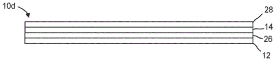
图1D示出了示例性制品10d的横向剖视图。制品10d可包括基底12、波长透射选择性层14、第一密封剂层26以及第二密封剂层28。第一密封剂层26和第二密封剂层28中的一者或多者可包括乳胶涂层。相应密封剂层可例如通过防止或减少水分或其他反应物或崩解剂的侵入来保护波长透射选择性层14的完整性。相应密封剂层也可对波长透射选择性层14提供结构支撑和物理稳定性。例如,第一密封剂层26和第二密封剂层28中的一者或两者可允许波长透射选择性层14从制造基底剥离或移除,然后输送并施加在产品基底上方,例如基底12上方。Figure ID shows a transverse cross-sectional view of an
图1E示出了示例性制品10e的横向剖视图。制品10e可包括基底12、与基底12相邻的波长透射选择性层14、以及沉积在波长透射选择性层14上的着墨图案层24。包括相应传感器区段32a、32b、32c和32d的传感器层32可与基底12相邻设置。在示例中,可省略基底12,并且波长透射选择性层14可沉积在传感器层32上。在示例中,波长透射选择性层14可包括可与相应传感器区段32a、32b、32c和32d对准的相应选择性散射区段14a、14b、14c和14d。可省略一个或多个选择性散射区段,使得波长透射选择性层14可包括可与相应传感器区段中的至少一个对准的至少一个穿孔。因此,可通过改变近红外散射比率、可见光雾度比率或者可改善与相应选择性散射区段对准的传感器区段的性能的其他光学属性来调节不同选择性散射区段。虽然图1E的波长散射层14和传感器层32中示出了四个区段,但在示例中,波长散射层14和传感器层32可具有任何合适数量的区段。虽然在图1E的示例中描述了传感器层32,但在示例中,制品10e可包括光源32a、32b、32c和32d,而不是传感器区段。FIG. 1E shows a transverse cross-sectional view of an
虽然图1A-图1E将相应制品10a-10e示为包括平整层,但是在各种示例中,制品10a-10e可呈现任何合适的形状、周边或横截面,并且制品10a-10e中的层可呈现规则、不规则或复合曲率,或者可在不同区域中呈现平整或弯曲的几何形状,或者以其他方式贴合层下方的基底或制品10a-10e的轮廓。例如,制品10a-10e可呈现半球状或透镜状形状。Although FIGS. 1A-1E show the
包括波长透射选择性粘合剂层的光学制品可用于各种系统,包括例如光学系统。此类光学滤光器可靠近或与光学系统的任何一个或多个部分相邻地使用。例如,光学滤光器可靠近光源、检测器、被检测对象或它们的任何组合使用。在其中光学制品靠近待检测的对象使用的一些实施方案中,反射器可包括在该光学制品中或靠近该光学制品。例示性反射器可包括镜面反射器、漫反射器、半镜面反射器、回射反射器或它们的任何组合。例示性回射器可包括含珠回射制品和立体角回射制品两者以及金属背衬或空气背衬中的任一者。在一些实施方案中,光学滤光器可被定位成在包括例如光纤或中空或实心光导的光传输装置附近、与光传输装置成一体、或同时采用这两种方式。Optical articles that include wavelength-transmissive selective adhesive layers can be used in a variety of systems, including, for example, optical systems. Such optical filters may be used near or adjacent to any portion or portions of the optical system. For example, optical filters can be used in close proximity to the light source, detector, object to be detected, or any combination thereof. In some embodiments where the optical article is used near the object to be detected, a reflector may be included in or near the optical article. Exemplary reflectors may include specular reflectors, diffuse reflectors, semi-specular reflectors, retroreflective reflectors, or any combination thereof. Exemplary retroreflectors may include both beaded retroreflective articles and cube corner retroreflective articles and either metal backings or air backings. In some embodiments, the optical filter can be positioned adjacent to the light delivery device including, for example, an optical fiber or a hollow or solid light guide, integral with the light delivery device, or both.
图2A-图2E为包括光学滤光器的示例性光学系统的概念图和示意图。图2A为包括光学滤光器10和光接收器40的示例性光学系统的概念图和示意图。在示例中,光接收器40可包括光传感器、相机、CCD或被配置为感测光的至少一个预定波长区域的任何其他传感器。例如,光接收器40可包括近红外传感器。在示例中,光接收器40可包括接收光的对象例如太阳能电池,或至少部分地吸收入射光的对象例如太阳能加热器,或接收光的任何其他对象。光学滤光器10可包括如以上参考图1A至图1E所讨论的包括波长透射选择性层的示例性光学滤光器中的任一个,或本公开中所述的其他示例性光学滤光器。如图2A所示,光学滤光器10可与光接收器40相邻设置。入射近红外线42a可包括近红外波长,并且可基本上透射穿过光学滤光器10至光接收器40。入射可见光线44a可包括可见光波长,并且可基本上被光学滤光器10反射或散射,使得光接收器40被至少部分地屏蔽可见光线44a,同时至少部分地接收近红外线42a。在示例中,光接收器可基本上或完全被光学滤光器10屏蔽可见光线44a,并且可接收基本上全部的近红外线42a。2A-2E are conceptual and schematic diagrams of exemplary optical systems including optical filters. FIG. 2A is a conceptual and schematic diagram of an exemplary optical system including
图2B为包括光学滤光器10、光接收器40、光发射器46和对象48的示例性光学系统的概念图和示意图。在示例中,光发射器46可包括任何合适波长的光源或电磁辐射源,包括可见光、近红外或紫外波长。在示例中,光发射器46可包括灯泡、白炽光源、紧凑型荧光灯、LED、光导或任何天然光源或人造光源。在示例中,光发射器46可不产生光,并且可仅反射或透射由光源产生的光。光学滤光器10可设置在光接收器40和对象48之间。光发射器可设置在光学滤光器10的与光接收器40相同的一侧上。从光发射器46透射的近红外线42b可包括近红外波长,并且可基本上透射穿过光学滤光器10至对象48。光线42b可被对象48反射回来,并且反射光线可通过对象48的光学属性进行修改。反射光线42可基本上透射穿过光学滤光器10至光接收器40。入射可见光线44b可包括可见光波长,并且可基本上被光学滤光器10反射或散射,使得光接收器40和光发射器46中的一者或两者被至少部分地屏蔽可见光线44a。在示例中,光接收器可基本上或完全被光学滤光器10屏蔽可见光线44b,并且可接收基本上全部的近红外线42b。FIG. 2B is a conceptual and schematic diagram of an exemplary optical system including
图2C为包括光学滤光器10、光接收器40和对象48的示例性光学系统的概念图和示意图。光学滤光器10可设置在光接收器40和对象48之间。入射近红外线42c可包括近红外波长,并且可基本上透射穿过对象48和光学滤光器10至光接收器40。入射可见光线44c可包括可见光波长,并且可基本上被光学滤光器10反射或散射,使得光接收器40被至少部分地屏蔽可见光线44c,同时至少部分地接收近红外线42c。在示例中,光接收器40可基本上或完全被光学滤光器10屏蔽可见光线44c,并且可接收基本上全部的近红外线42c。FIG. 2C is a conceptual and schematic diagram of an exemplary optical system including
图2D为包括光学滤光器10和光接收器40的示例性光学系统的概念图和示意图。光学滤光器10可与光接收器40相邻设置。入射近红外线42d可包括近红外波长,并且可基本上从光学滤光器10反射至光接收器40。入射可见光线44d可包括可见光波长,并且可基本上被光学滤光器10反射或散射,使得光接收器40至少部分地接收可见光线44d,同时至少部分地接收近红外线42d。FIG. 2D is a conceptual and schematic diagram of an exemplary optical system including
图2E为包括光学滤光器10、光接收器40和光发射器46的示例性光学系统的概念图和示意图。光学滤光器10可设置在光发射器46和光接收器40之间。从光发射器46透射的近红外线42e可包括近红外波长,并且可基本上透射穿过光学滤光器10至光接收器40。入射可见光线44e可包括可见光波长,并且可基本上被光学滤光器10反射或散射,使得光发射器46至少部分地屏蔽可见光线44e。在示例中,光发射器46可基本上或完全被光学滤光器10屏蔽可见光线44e。虽然图2E的示例性光学系统中描述了光接收器40,但在示例中,图2E的示例性光学系统可不包括光接收器40。例如,示例性光学系统可包括光发射器46和光学滤光器10,并且光学滤光器10可隐蔽光发射器46的可见外观。FIG. 2E is a conceptual and schematic diagram of an exemplary optical system including
在示例中,光学滤光器10可包括至少一个可移除的或可重新定位的层,或者光学滤光器10作为整体可为可移除的或可重新定位的,使得其相对于位于光学滤光器10下方或与其相邻的基底可被移除或重新定位。在示例中,光学滤光器10的外围可延伸超出光发射器46或光接收器40中的一者或两者的外围,或者光学滤光器10的主表面的面积可大于或小于光发射器46或光接收器40中的一者或两者的表面积。在示例中,光学滤光器10可被配置为掩蔽其他部件,诸如电子器件、电路、基底、传感器、发射器,通过光学滤光器屏蔽这些部件使其不被视觉感知。在示例中,多于一个的光发射器46或光接收器40(例如,阵列)可与光学滤光器10相邻定位。在示例中,光发射器46或光接收器40中的一者或两者可相对远离光学滤光器10,例如距离至少1cm、或距离10cm、或距离1m、距离10m、或距离100m、或距离1km、或甚至更远。虽然在图2A-图2E中示出了光的直接路径,例如,在光发射器46和光接收器40中的一者或两者与光学滤光器10之间,但在示例中,光发射器46和光接收器40中的一者或两者与光学滤光器10之间的光可沿循间接路径,包括光学导向路径、反射路径或包括光学操控(包括折射或滤光)的路径、或穿过不同光学介质行进的路径。In an example, the
因此,在示例中,光学滤光器10可被配置为对光接收器40至少部分地屏蔽可见光波长,同时基本上允许光接收器40接收近红外波长。在示例中,光学滤光器10可被配置为例如通过散射可见波长掩蔽光接收器40或光发射器46中的一者或两者使其不被视觉感知。Thus, in an example, the
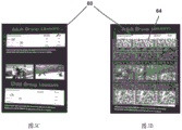
图3A-图3D为示例性系统的概念图,该示例性系统包括示例性光学滤光器以及显示可视觉感知图案和不可见近红外图案的电子显示器。由于成像传感器诸如电荷耦合器件(CCD)在近红外区域中进行检测,将可能产生包括视觉反射图形的标志。该标志可隐蔽可由相机检测到的不可见图像。例如,图像可包括对信号或信息进行编码的预定图案,诸如条形码、2D条形码、或QR码。QR码的物理大小可限制它们可包含的信息量。然而,不可见QR码可与标志物理上一样大,而不会混淆或减损可见图形。在一个示例中,电子显示器60可能够同时显示由隐蔽在显示器60后方的相应可见光发射器和近红外光发射器发射的可见图案和近红外图案。可用上文参考图1A至图1E所述的示例性光学滤光器覆盖电子显示器60。例如,电子显示器60可同时显示可见图案62和不可见的近红外图案64,如图3B所示。图案62可包括相对较小的QR码或带有相对较小的显示占有面积的其他标记,而图案64可包括相对较大的QR码或具有相对较大占有面积的其他标记。图案62可由于光学滤光器(未示出)对可见波长的反射或散射而可见。如图3A所见,仅图案62可被视觉感知,并且图案64可保持对视觉感知不可见,而在近红外波长下呈现相对高的清晰度。因此,能够感测近红外波长的相机可以足够的分辨率(例如足以对可包含在图案64中的信息进行解码的分辨率)来感测图案64。在图3C所示的示例中,只有预定图案可在显示器60上被视觉感知,而如图3D所示,只有近红外相机才可检测到的不可见近红外图案可同时显示在显示器60上。因此,在图3A和图3B以及图3C和图3D的相应示例性系统中,示例性光学滤光器可用于隐蔽或掩蔽近红外图案的源,同时仅显露预定可见图案。在一些示例中,不可见近红外图案64可用于对隐藏信息进行编码,而视觉感知图案62可用于呈现可视觉感知信息,或至少可被编码但可视觉感知为被编码的信息。例如,图案62可对第一组信息诸如网站进行编码,而图案64可对第二组信息诸如显示器60的位置进行编码。在示例中,电子显示器60可显示可见图案、不可见图案或两者。在示例中,电子显示器60可显示多个图案。在示例中,电子显示器可显示静态图案或动态图案。因此,示例性光学滤光器可以高透明度的近红外透射提供掩蔽。3A-3D are conceptual diagrams of an exemplary system including an exemplary optical filter and an electronic display displaying a visually perceptible pattern and an invisible near-infrared pattern. Since imaging sensors such as charge coupled devices (CCDs) detect in the near infrared region, it will be possible to generate signs that include visual reflection patterns. This sign conceals invisible images that can be detected by the camera. For example, the image may include a predetermined pattern that encodes a signal or information, such as a barcode, 2D barcode, or QR code. The physical size of QR codes can limit the amount of information they can contain. However, the invisible QR code can be physically as large as the logo without confusing or detracting from the visible graphics. In one example,
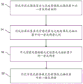
图4为示例性技术的流程图。该示例性技术可包括将光学滤光器10设置为与光发射器46或光接收器40中的一者或两者相邻(52)。光学滤光器10包括如上文参考图1A至图1E和图2A至图2E所讨论的波长透射选择性层。该示例性技术还可任选地包括将反射层16设置在光学滤光器10与光发射器46或光接收器40中的一者或两者之间(54)。光学滤光器10可任选地掩蔽光发射器46或光接收器40中的一者或两者(56)。光学滤光器10可任选地对光发射器或光接收器中的一者或两者至少部分地屏蔽可见光波长(58)。4 is a flow diagram of an exemplary technique. The exemplary technique may include positioning the
因此,根据本公开的示例性系统、制品和技术可包括示例性光学制品,该示例性光学制品包括示例性波长透射选择性层,该波长透射选择性层例如通过选择性地散射、吸收或反射可见光波长,以相对高的透明度透射近红外光,同时减少可见光波长的透射。Thus, exemplary systems, articles, and techniques according to the present disclosure may include exemplary optical articles that include exemplary wavelength transmission selective layers, such as by selectively scattering, absorbing, or reflecting Visible wavelengths, transmit near-infrared light with relatively high transparency, while reducing transmission of visible wavelengths.
除非另外指明,否则本文所使用的所有科学和技术术语具有在本领域中普遍使用的含义。本文提供的定义将有利于理解本文频繁使用的某些术语,并且不意味着限制本公开的范围。Unless otherwise specified, all scientific and technical terms used herein have the meaning commonly used in the art. Definitions provided herein will facilitate understanding of certain terms frequently used herein and are not meant to limit the scope of the present disclosure.
除非内容另外明确指明,否则如本说明书和所附权利要求中使用的,单数形式“一个”、“一种”和“所述”涵盖具有多个指代物的实施方案。As used in this specification and the appended claims, the singular forms "a," "an," and "the" encompass embodiments having plural referents unless the content clearly dictates otherwise.
除非内容另外明确指明,否则如本说明书和所附权利要求书中使用的,术语“或”一般以其包括“和/或”的意义采用。术语“和/或”意指所列要素中的一个或全部,或者所列要素中的任何两个或更多个的组合。As used in this specification and the appended claims, the term "or" is generally employed in its sense including "and/or" unless the content clearly dictates otherwise. The term "and/or" means one or all of the listed elements or a combination of any two or more of the listed elements.
如本文所用,“具有”、“包括”、“包含”等等均以其开放性意义使用,并且一般是指“包括但不限于”。应当理解,“基本上由……组成”、“由……组成”等等包含在“包括”等等之中。例如,“包括”银的组合物可以是“由银组成”或“基本上由银组成”的组合物。As used herein, "having", "including", "including" and the like are used in their open-ended sense and generally mean "including but not limited to". It should be understood that "consisting essentially of," "consisting of," and the like are included in "comprising," and the like. For example, a composition that "comprises" silver can be a composition that "consists of silver" or "consists essentially of silver."
如本文所用,当“基本上由……组成”涉及组合物、设备、系统、方法等等时,意味着这些组合物、设备、系统、方法等等的组成要素限于所枚举的组成要素,以及对这些组合物、设备、系统、方法等等的基本特性和新颖特性无实质性影响的任何其他组成要素。As used herein, when "consisting essentially of" in reference to a composition, device, system, method, etc., it means that the components of such composition, device, system, method, etc. are limited to the enumerated components, and any other constituent elements that do not materially affect the basic and novel characteristics of these compositions, devices, systems, methods, etc.
词语“优选的”和“优选地”是指在某些情况下可提供某些有益效果的实施方案。然而,在相同的情况或其他情况下,其他实施方案也可以是优选的。此外,对一个或多个优选实施方案的表述并不暗示其他实施方案是不可用的,并且并不旨在将其他实施方案排除在本公开(包括权利要求书)的范围之外。The words "preferred" and "preferably" refer to embodiments that may provide certain benefits under certain circumstances. However, other embodiments may also be preferred, under the same or other circumstances. Furthermore, the recitation of one or more preferred embodiments does not imply that other embodiments are not available, and is not intended to exclude other embodiments from the scope of this disclosure, including the claims.
另外,在本文中,通过端点表述的数值范围包括该范围内所含的所有数值(例如,1至5包括1、1.5、2、2.75、3、3.80、4、5等,或者10或更少,包括10、9.4、7.6、5、4.3、2.9、1.62、0.3等)。当值的范围“多达”某个特定值时,该值包括在该范围内。Also, herein, the recitation of numerical ranges by endpoints includes all numbers subsumed within that range (eg, 1 to 5 includes 1, 1.5, 2, 2.75, 3, 3.80, 4, 5, etc., or 10 or less) , including 10, 9.4, 7.6, 5, 4.3, 2.9, 1.62, 0.3, etc.). When a range of values is "up to" a particular value, that value is included in that range.
在以上描述和以下权利要求中使用“第一”、“第二”等并不一定旨在表示存在枚举数量的对象。例如,“第二”基底仅旨在与另一基底(诸如“第一”基底)区分开。在以上描述和随后的权利要求中使用“第一”、“第二”也不一定旨在表示一个在时间上早于另一个。The use of "first," "second," etc. in the above description and the following claims is not necessarily intended to mean that there is an enumerated number of objects. For example, a "second" substrate is only intended to be distinguished from another substrate, such as a "first" substrate. The use of "first" and "second" in the above description and the following claims is also not necessarily intended to mean that one is earlier than the other in time.
根据本公开的示例性制品和技术将通过以下非限制性实施例来说明。Exemplary articles and techniques in accordance with the present disclosure will be illustrated by the following non-limiting examples.
表1Table 1


测试方法testing method
使用光谱仪(Hunterlab Ultrascan Pro)以5nm间隔测量了可见光(400nm-700nm)和近红外(800nm-1000nm)总透射率和漫透射率。实施例1至7的在365nm、475nm、525nm、650nm、700nm、750nm、800nm、850nm、875nm、900nm、940nm和975nm处的透射百分比(%T)已记录在下表2中。Visible (400nm-700nm) and near-infrared (800nm-1000nm) total and diffuse transmittances were measured at 5nm intervals using a spectrometer (Hunterlab Ultrascan Pro). The percent transmission (%T) at 365 nm, 475 nm, 525 nm, 650 nm, 700 nm, 750 nm, 800 nm, 850 nm, 875 nm, 900 nm, 940 nm and 975 nm for Examples 1 to 7 are reported in Table 2 below.
涂层溶液coating solution
涂层溶液1:将9克Nazdar NSC61用7克Nazdar RE195稀释剂/丝网清洗剂稀释以制成稀释的丝网油墨或涂层溶液1。Coating Solution 1: Dilute 9 grams of Nazdar NSC61 with 7 grams of Nazdar RE195 Thinner/Screen Cleaner to make Diluted Screen Ink or Coating Solution 1.
涂层溶液2:在60℃下,在封闭的玻璃广口瓶中将210克Paraloid B66溶解在210克MEK中。将75克Orasol Black X55溶解在300克MEK中。将Orasol Black X55溶液添加到MEK中的Paraloid B66溶液(如上制得)中以制备涂层溶液2。Coating solution 2: Dissolve 210 grams of Paraloid B66 in 210 grams of MEK in a closed glass jar at 60°C. Dissolve 75 grams of Orasol Black X55 in 300 grams of MEK. The Orasol Black X55 solution was added to the Paraloid B66 solution in MEK (prepared as above) to prepare Coating Solution 2.
涂层溶液3:将溶解于甲苯中的1克10重量%IR 788添加到2克涂层溶液2中以制备涂层溶液3。Coating Solution 3: Coating Solution 3 was prepared by adding 1 gram of 10 wt% IR 788 dissolved in toluene to 2 grams of Coating Solution 2.
实施例1Example 1
用#20Meyer棒将涂层溶液1涂覆在有色PET膜(YS-7)上。将经涂覆的样品在烘箱中以70℃干燥5分钟,之后将该样品风干1天。Coating Solution 1 was coated on a colored PET film (YS-7) with a #20 Meyer rod. The coated samples were dried in an oven at 70°C for 5 minutes, after which the samples were air dried for 1 day.
实施例2Example 2
用#20Meyer棒将涂层溶液1涂覆在有色PET膜(YS-35)上。将经涂覆的样品在烘箱中以70℃干燥5分钟,之后将该样品风干1天。Coating Solution 1 was coated on a colored PET film (YS-35) with a #20 Meyer rod. The coated samples were dried in an oven at 70°C for 5 minutes, after which the samples were air dried for 1 day.
实施例3Example 3
用#20Meyer棒将涂层溶液1涂覆在有色PET膜(CP-20)上。将经涂覆的样品在烘箱中以70℃干燥5分钟,之后将该样品风干1天。Coating Solution 1 was coated on a colored PET film (CP-20) with a #20 Meyer rod. The coated samples were dried in an oven at 70°C for 5 minutes, after which the samples were air dried for 1 day.
实施例4至6Examples 4 to 6
在涂布机上将涂层溶液2以三种不同的涂覆重量(每分钟12cc、8cc和4cc)涂覆在YS-7膜(5英寸宽)上,涂覆宽度为4英寸。将经涂覆的幅材在100℉、110℉和140℉下的一系列烘箱中干燥。实施例4、5和6的经涂覆的膜的光密度分别测量为5.4、4.5和3.4。Coating Solution 2 was applied to YS-7 film (5 inches wide) on a coater at three different coat weights (12 cc, 8 cc and 4 cc per minute) with a coating width of 4 inches. The coated webs were dried in a series of ovens at 100°F, 110°F and 140°F. The optical densities of the coated films of Examples 4, 5 and 6 were measured to be 5.4, 4.5 and 3.4, respectively.
实施例7Example 7
用#20Meyer棒将涂层溶液3涂覆在有色PET膜(YS-7)上。将经涂覆的样品在烘箱中以70℃干燥5分钟,之后将该样品风干1天。Coating Solution 3 was coated on a colored PET film (YS-7) with a #20 Meyer rod. The coated samples were dried in an oven at 70°C for 5 minutes, after which the samples were air dried for 1 day.
使用Hunterlab Ultrascan Pro光谱仪测量了实施例1至6中经涂覆的膜的总透射率和漫透射率。使用940nm处的漫透射率与总透射率的比率来计算940nm处的红外散射率。图5示出了经涂覆的样品的总透射光谱。表2示出了940nm处的镜面透射率和940nm处的红外散射率(百分比)。测量结果表明,这些膜表现出高可见光阻挡性、高近红外透射率(该近红外透射率是可调节的),并且在940nm处具有非常低的漫射近红外散射,如根据940nm处的漫透射率/总透射率的比率计算的少于1%的近红外散射率所证实的。The total and diffuse transmission of the coated films of Examples 1 to 6 were measured using a Hunterlab Ultrascan Pro spectrometer. Infrared scattering at 940 nm was calculated using the ratio of diffuse transmittance to total transmittance at 940 nm. Figure 5 shows the total transmission spectrum of the coated samples. Table 2 shows the specular transmittance at 940 nm and the infrared scattering rate (percent) at 940 nm. Measurements show that these films exhibit high visible light blocking, high near-infrared transmittance (which is tunable), and very low diffuse near-infrared scattering at 940 nm, as measured by the diffuse NIR at 940 nm. The ratio of transmittance/total transmittance was calculated as evidenced by a near-infrared scattering rate of less than 1%.
表2Table 2

因此公开了光学制品和包括该光学制品的系统的实施方案。上述实施方式以及其他实施方式均在以下权利要求书的范围内。本领域的技术人员将会知道,本公开可通过除所公开的那些实施方案之外的实施方案进行实施。所公开的实施方案仅出于举例说明目的,而非出于限制的目的。Embodiments of optical articles and systems including the same are thus disclosed. The above-described embodiments, as well as other embodiments, are within the scope of the following claims. Those skilled in the art will appreciate that the present disclosure may be practiced in embodiments other than those disclosed. The disclosed embodiments are for purposes of illustration only, and not for purpose of limitation.
Claims (43)
Applications Claiming Priority (3)
| Application Number | Priority Date | Filing Date | Title |
|---|---|---|---|
| US201762582500P | 2017-11-07 | 2017-11-07 | |
| US62/582,500 | 2017-11-07 | ||
| PCT/IB2018/058721 WO2019092598A1 (en) | 2017-11-07 | 2018-11-06 | Optical films and systems including the same |
Publications (1)
| Publication Number | Publication Date |
|---|---|
| CN111263903A true CN111263903A (en) | 2020-06-09 |
Family
ID=66439155
Family Applications (1)
| Application Number | Title | Priority Date | Filing Date |
|---|---|---|---|
| CN201880068287.8A Pending CN111263903A (en) | 2017-11-07 | 2018-11-06 | Optical film and system including the same |
Country Status (4)
| Country | Link |
|---|---|
| US (1) | US11619771B2 (en) |
| JP (1) | JP7580271B2 (en) |
| CN (1) | CN111263903A (en) |
| WO (1) | WO2019092598A1 (en) |
Families Citing this family (1)
| Publication number | Priority date | Publication date | Assignee | Title |
|---|---|---|---|---|
| JP7482380B2 (en) * | 2019-11-05 | 2024-05-14 | 日本電気株式会社 | Imaging device |
Citations (3)
| Publication number | Priority date | Publication date | Assignee | Title |
|---|---|---|---|---|
| US5518810A (en) * | 1993-06-30 | 1996-05-21 | Mitsubishi Materials Corporation | Infrared ray cutoff material and infrared cutoff powder use for same |
| WO2017127734A1 (en) * | 2016-01-21 | 2017-07-27 | 3M Innovative Properties Company | Optical camouflage filters |
| WO2017124664A1 (en) * | 2016-01-21 | 2017-07-27 | 3M Innovative Properties Company | Optical camouflage filters |
Family Cites Families (27)
| Publication number | Priority date | Publication date | Assignee | Title |
|---|---|---|---|---|
| IL74159A (en) * | 1985-01-25 | 1990-01-18 | Univ Ramot | Filtration of solar radiation through copper chloride solution |
| JPS62903A (en) * | 1985-06-05 | 1987-01-06 | Sumitomo Chem Co Ltd | Near infrared ray absorbing filter |
| JPH0333173A (en) * | 1989-06-29 | 1991-02-13 | Matsushita Electric Ind Co Ltd | Near infrared-absorbing adhesive |
| JPH058502U (en) * | 1991-07-23 | 1993-02-05 | 日本ビクター株式会社 | Infrared transparent filter |
| US6174400B1 (en) * | 1997-03-04 | 2001-01-16 | Isotag Technology, Inc. | Near infrared fluorescent security thermal transfer printing and marking ribbons |
| JPH1138892A (en) * | 1997-07-17 | 1999-02-12 | Ado Union Kenkyusho:Kk | Optical resin panel |
| US6024455A (en) * | 1998-01-13 | 2000-02-15 | 3M Innovative Properties Company | Reflective article with concealed retroreflective pattern |
| JP2001194524A (en) * | 2000-01-13 | 2001-07-19 | Fuji Photo Film Co Ltd | Optical filter, front plate and picture display device using same |
| JP2002122731A (en) * | 2000-10-17 | 2002-04-26 | Fuji Photo Film Co Ltd | Optical filter |
| JP5257642B2 (en) * | 2000-12-04 | 2013-08-07 | 住友電気工業株式会社 | Ceramic optical component and manufacturing method thereof |
| US6991849B2 (en) * | 2001-06-21 | 2006-01-31 | Teijin Limited | Near infrared ray shielding film |
| US7264169B2 (en) * | 2004-08-02 | 2007-09-04 | Idx, Inc. | Coaligned bar codes and validation means |
| JP2006319251A (en) * | 2005-05-16 | 2006-11-24 | Dainippon Printing Co Ltd | Composite electromagnetic wave shield filter |
| JP4468902B2 (en) * | 2006-01-17 | 2010-05-26 | 株式会社資生堂 | LAMINATED MATERIAL RECORDING INFORMATION, ARTICLE HAVING IT, AND INFORMATION READING METHOD |
| US7727418B2 (en) * | 2006-06-19 | 2010-06-01 | Sabic Innovative Plastics Ip B.V. | Infrared transmissive thermoplastic composition, and articles formed therefrom |
| JP2009069822A (en) * | 2007-08-22 | 2009-04-02 | Mitsubishi Chemicals Corp | Resin black matrix, light blocking photosensitive resin composition, tft element substrate and liquid crystal display device |
| JP5874116B2 (en) * | 2009-07-30 | 2016-03-02 | 国立研究開発法人産業技術総合研究所 | Image photographing apparatus and image photographing method |
| TW201435830A (en) * | 2012-12-11 | 2014-09-16 | 3M Innovative Properties Co | Inconspicuous optical tags and methods therefor |
| WO2014201559A1 (en) * | 2013-06-17 | 2014-12-24 | Corporation De L'ecole Polytechnique De Montreal | Interference security image structure |
| JP6282142B2 (en) * | 2014-03-03 | 2018-02-21 | 日東電工株式会社 | Infrared reflective substrate and manufacturing method thereof |
| KR102356199B1 (en) | 2014-03-07 | 2022-01-28 | 쓰리엠 이노베이티브 프로퍼티즈 컴파니 | Durable extruded dyed polyester films |
| WO2015155357A1 (en) * | 2014-04-10 | 2015-10-15 | CSEM Centre Suisse d'Electronique et de Microtechnique SA - Recherche et Développement | Infrared transmitting cover sheet |
| WO2016117452A1 (en) * | 2015-01-19 | 2016-07-28 | 旭硝子株式会社 | Optical device and optical member |
| CN107076895B (en) * | 2015-04-23 | 2019-06-14 | Agc株式会社 | Optical Filters and Cameras |
| JPWO2017043586A1 (en) | 2015-09-08 | 2018-06-28 | 国立大学法人京都大学 | Method for synthesizing metal sulfur halide and / or metal selenium halide using metal oxyhalide as raw material, and method for producing semiconductor member using the same |
| JP6927559B2 (en) * | 2015-12-17 | 2021-09-01 | 株式会社テララコード研究所 | Optical code, optical code creation method, optical code authenticity determination method, optical code reader, and reading aid |
| WO2019092597A1 (en) | 2017-11-07 | 2019-05-16 | 3M Innovative Properties Company | Optical articles and systems including the same |
-
2018
- 2018-11-06 US US16/652,996 patent/US11619771B2/en active Active
- 2018-11-06 CN CN201880068287.8A patent/CN111263903A/en active Pending
- 2018-11-06 WO PCT/IB2018/058721 patent/WO2019092598A1/en active Application Filing
- 2018-11-06 JP JP2020524906A patent/JP7580271B2/en active Active
Patent Citations (3)
| Publication number | Priority date | Publication date | Assignee | Title |
|---|---|---|---|---|
| US5518810A (en) * | 1993-06-30 | 1996-05-21 | Mitsubishi Materials Corporation | Infrared ray cutoff material and infrared cutoff powder use for same |
| WO2017127734A1 (en) * | 2016-01-21 | 2017-07-27 | 3M Innovative Properties Company | Optical camouflage filters |
| WO2017124664A1 (en) * | 2016-01-21 | 2017-07-27 | 3M Innovative Properties Company | Optical camouflage filters |
Also Published As
| Publication number | Publication date |
|---|---|
| US20200292737A1 (en) | 2020-09-17 |
| WO2019092598A1 (en) | 2019-05-16 |
| JP7580271B2 (en) | 2024-11-11 |
| US11619771B2 (en) | 2023-04-04 |
| JP2021501918A (en) | 2021-01-21 |
Similar Documents
| Publication | Publication Date | Title |
|---|---|---|
| JP7438267B2 (en) | optical camouflage filter | |
| CN108496098B (en) | Optical masking filter | |
| US9562998B2 (en) | Inconspicuous optical tags and methods therefor | |
| WO2017110939A1 (en) | Optical filter and optical device | |
| JP7456927B2 (en) | optical camouflage filter | |
| KR20210087991A (en) | How to detect hidden patterns | |
| CN111316137B (en) | Optical article and system including the same | |
| KR20160067139A (en) | Decorative microsphere articles | |
| CN111263903A (en) | Optical film and system including the same |
Legal Events
| Date | Code | Title | Description |
|---|---|---|---|
| PB01 | Publication | ||
| PB01 | Publication | ||
| SE01 | Entry into force of request for substantive examination | ||
| SE01 | Entry into force of request for substantive examination | ||
| RJ01 | Rejection of invention patent application after publication |
Application publication date: 20200609 |
|
| RJ01 | Rejection of invention patent application after publication |