CN111196802A - Compound, organic electronic device comprising the same, and display apparatus and lighting apparatus comprising the same - Google Patents
Compound, organic electronic device comprising the same, and display apparatus and lighting apparatus comprising the same Download PDFInfo
- Publication number
- CN111196802A CN111196802A CN201911117538.XA CN201911117538A CN111196802A CN 111196802 A CN111196802 A CN 111196802A CN 201911117538 A CN201911117538 A CN 201911117538A CN 111196802 A CN111196802 A CN 111196802A
- Authority
- CN
- China
- Prior art keywords
- group
- compound
- layer
- formula
- electronic device
- Prior art date
- Legal status (The legal status is an assumption and is not a legal conclusion. Google has not performed a legal analysis and makes no representation as to the accuracy of the status listed.)
- Pending
Links
- 150000001875 compounds Chemical class 0.000 title claims abstract description 154
- 230000000903 blocking effect Effects 0.000 claims description 48
- 125000003118 aryl group Chemical group 0.000 claims description 46
- 239000004065 semiconductor Substances 0.000 claims description 39
- 125000004429 atom Chemical group 0.000 claims description 31
- JEGZRTMZYUDVBF-UHFFFAOYSA-N Benz[a]acridine Chemical group C1=CC=C2C3=CC4=CC=CC=C4N=C3C=CC2=C1 JEGZRTMZYUDVBF-UHFFFAOYSA-N 0.000 claims description 16
- 229910052757 nitrogen Inorganic materials 0.000 claims description 15
- 229910052760 oxygen Inorganic materials 0.000 claims description 11
- 125000004432 carbon atom Chemical group C* 0.000 claims description 9
- 125000003968 arylidene group Chemical group [H]C(c)=* 0.000 claims description 8
- 125000005842 heteroatom Chemical group 0.000 claims description 8
- 229910052717 sulfur Inorganic materials 0.000 claims description 8
- 125000001424 substituent group Chemical group 0.000 claims description 7
- 125000000609 carbazolyl group Chemical class C1(=CC=CC=2C3=CC=CC=C3NC12)* 0.000 claims description 2
- 125000004986 diarylamino group Chemical class 0.000 claims description 2
- 229910052739 hydrogen Inorganic materials 0.000 claims description 2
- 238000002347 injection Methods 0.000 description 40
- 239000007924 injection Substances 0.000 description 40
- 238000000151 deposition Methods 0.000 description 32
- 239000000463 material Substances 0.000 description 32
- 239000000758 substrate Substances 0.000 description 31
- 230000005525 hole transport Effects 0.000 description 29
- 239000002019 doping agent Substances 0.000 description 28
- -1 benzacridine compound Chemical class 0.000 description 27
- YXFVVABEGXRONW-UHFFFAOYSA-N Toluene Chemical compound CC1=CC=CC=C1 YXFVVABEGXRONW-UHFFFAOYSA-N 0.000 description 24
- 230000008021 deposition Effects 0.000 description 23
- 239000011248 coating agent Substances 0.000 description 16
- 238000000576 coating method Methods 0.000 description 16
- 229910052751 metal Inorganic materials 0.000 description 16
- 239000002184 metal Chemical class 0.000 description 16
- IMKMFBIYHXBKRX-UHFFFAOYSA-M lithium;quinoline-2-carboxylate Chemical compound [Li+].C1=CC=CC2=NC(C(=O)[O-])=CC=C21 IMKMFBIYHXBKRX-UHFFFAOYSA-M 0.000 description 15
- 150000003254 radicals Chemical group 0.000 description 15
- VLKZOEOYAKHREP-UHFFFAOYSA-N n-Hexane Chemical compound CCCCCC VLKZOEOYAKHREP-UHFFFAOYSA-N 0.000 description 14
- 239000007787 solid Substances 0.000 description 14
- YMWUJEATGCHHMB-UHFFFAOYSA-N Dichloromethane Chemical compound ClCCl YMWUJEATGCHHMB-UHFFFAOYSA-N 0.000 description 12
- 238000004770 highest occupied molecular orbital Methods 0.000 description 12
- 239000011777 magnesium Substances 0.000 description 11
- 229910052783 alkali metal Inorganic materials 0.000 description 10
- 239000000203 mixture Substances 0.000 description 10
- OKKJLVBELUTLKV-UHFFFAOYSA-N Methanol Chemical compound OC OKKJLVBELUTLKV-UHFFFAOYSA-N 0.000 description 9
- 238000000034 method Methods 0.000 description 9
- 239000002244 precipitate Substances 0.000 description 9
- 238000004528 spin coating Methods 0.000 description 9
- 238000001771 vacuum deposition Methods 0.000 description 9
- 125000001072 heteroaryl group Chemical group 0.000 description 8
- 229910052749 magnesium Inorganic materials 0.000 description 8
- 238000000967 suction filtration Methods 0.000 description 8
- 239000000654 additive Substances 0.000 description 7
- 150000001340 alkali metals Chemical class 0.000 description 7
- 229910052784 alkaline earth metal Inorganic materials 0.000 description 7
- 125000000217 alkyl group Chemical group 0.000 description 7
- 239000011575 calcium Substances 0.000 description 7
- 230000000052 comparative effect Effects 0.000 description 7
- 238000004768 lowest unoccupied molecular orbital Methods 0.000 description 7
- 239000011159 matrix material Substances 0.000 description 7
- 229910052709 silver Inorganic materials 0.000 description 7
- 239000004332 silver Substances 0.000 description 7
- IXHWGNYCZPISET-UHFFFAOYSA-N 2-[4-(dicyanomethylidene)-2,3,5,6-tetrafluorocyclohexa-2,5-dien-1-ylidene]propanedinitrile Chemical compound FC1=C(F)C(=C(C#N)C#N)C(F)=C(F)C1=C(C#N)C#N IXHWGNYCZPISET-UHFFFAOYSA-N 0.000 description 6
- HEDRZPFGACZZDS-UHFFFAOYSA-N Chloroform Chemical compound ClC(Cl)Cl HEDRZPFGACZZDS-UHFFFAOYSA-N 0.000 description 6
- BQCADISMDOOEFD-UHFFFAOYSA-N Silver Chemical compound [Ag] BQCADISMDOOEFD-UHFFFAOYSA-N 0.000 description 6
- 229910052769 Ytterbium Inorganic materials 0.000 description 6
- 229910052791 calcium Inorganic materials 0.000 description 6
- 238000007639 printing Methods 0.000 description 6
- 239000000126 substance Substances 0.000 description 6
- XLYOFNOQVPJJNP-UHFFFAOYSA-N water Substances O XLYOFNOQVPJJNP-UHFFFAOYSA-N 0.000 description 6
- 150000001342 alkaline earth metals Chemical class 0.000 description 5
- 150000004646 arylidenes Chemical group 0.000 description 5
- 238000005266 casting Methods 0.000 description 5
- 239000000306 component Substances 0.000 description 5
- 230000006866 deterioration Effects 0.000 description 5
- 238000001035 drying Methods 0.000 description 5
- 125000006575 electron-withdrawing group Chemical group 0.000 description 5
- 239000011521 glass Substances 0.000 description 5
- 150000002430 hydrocarbons Chemical group 0.000 description 5
- 229910052744 lithium Inorganic materials 0.000 description 5
- SKEDXQSRJSUMRP-UHFFFAOYSA-N lithium;quinolin-8-ol Chemical compound [Li].C1=CN=C2C(O)=CC=CC2=C1 SKEDXQSRJSUMRP-UHFFFAOYSA-N 0.000 description 5
- 238000000746 purification Methods 0.000 description 5
- 230000005855 radiation Effects 0.000 description 5
- 239000000725 suspension Substances 0.000 description 5
- LFQSCWFLJHTTHZ-UHFFFAOYSA-N Ethanol Chemical compound CCO LFQSCWFLJHTTHZ-UHFFFAOYSA-N 0.000 description 4
- 229910052693 Europium Inorganic materials 0.000 description 4
- JUJWROOIHBZHMG-UHFFFAOYSA-N Pyridine Chemical compound C1=CC=NC=C1 JUJWROOIHBZHMG-UHFFFAOYSA-N 0.000 description 4
- 230000000996 additive effect Effects 0.000 description 4
- 229910052788 barium Inorganic materials 0.000 description 4
- 229910052792 caesium Inorganic materials 0.000 description 4
- 239000003795 chemical substances by application Substances 0.000 description 4
- 150000004696 coordination complex Chemical class 0.000 description 4
- 238000002330 electrospray ionisation mass spectrometry Methods 0.000 description 4
- 238000000295 emission spectrum Methods 0.000 description 4
- 125000001153 fluoro group Chemical group F* 0.000 description 4
- 238000004128 high performance liquid chromatography Methods 0.000 description 4
- 238000005286 illumination Methods 0.000 description 4
- 238000004519 manufacturing process Methods 0.000 description 4
- IBHBKWKFFTZAHE-UHFFFAOYSA-N n-[4-[4-(n-naphthalen-1-ylanilino)phenyl]phenyl]-n-phenylnaphthalen-1-amine Chemical compound C1=CC=CC=C1N(C=1C2=CC=CC=C2C=CC=1)C1=CC=C(C=2C=CC(=CC=2)N(C=2C=CC=CC=2)C=2C3=CC=CC=C3C=CC=2)C=C1 IBHBKWKFFTZAHE-UHFFFAOYSA-N 0.000 description 4
- 229920000767 polyaniline Polymers 0.000 description 4
- 229910052700 potassium Inorganic materials 0.000 description 4
- BWHMMNNQKKPAPP-UHFFFAOYSA-L potassium carbonate Chemical compound [K+].[K+].[O-]C([O-])=O BWHMMNNQKKPAPP-UHFFFAOYSA-L 0.000 description 4
- 229910052701 rubidium Inorganic materials 0.000 description 4
- 229910052708 sodium Inorganic materials 0.000 description 4
- 229910052712 strontium Inorganic materials 0.000 description 4
- VQGHOUODWALEFC-UHFFFAOYSA-N 2-phenylpyridine Chemical compound C1=CC=CC=C1C1=CC=CC=N1 VQGHOUODWALEFC-UHFFFAOYSA-N 0.000 description 3
- AWXGSYPUMWKTBR-UHFFFAOYSA-N 4-carbazol-9-yl-n,n-bis(4-carbazol-9-ylphenyl)aniline Chemical compound C12=CC=CC=C2C2=CC=CC=C2N1C1=CC=C(N(C=2C=CC(=CC=2)N2C3=CC=CC=C3C3=CC=CC=C32)C=2C=CC(=CC=2)N2C3=CC=CC=C3C3=CC=CC=C32)C=C1 AWXGSYPUMWKTBR-UHFFFAOYSA-N 0.000 description 3
- 101000837344 Homo sapiens T-cell leukemia translocation-altered gene protein Proteins 0.000 description 3
- FYYHWMGAXLPEAU-UHFFFAOYSA-N Magnesium Chemical compound [Mg] FYYHWMGAXLPEAU-UHFFFAOYSA-N 0.000 description 3
- VYPSYNLAJGMNEJ-UHFFFAOYSA-N Silicium dioxide Chemical compound O=[Si]=O VYPSYNLAJGMNEJ-UHFFFAOYSA-N 0.000 description 3
- 102100028692 T-cell leukemia translocation-altered gene protein Human genes 0.000 description 3
- 150000001339 alkali metal compounds Chemical class 0.000 description 3
- 150000004945 aromatic hydrocarbons Chemical group 0.000 description 3
- 229910052799 carbon Inorganic materials 0.000 description 3
- 238000001816 cooling Methods 0.000 description 3
- IOJUPLGTWVMSFF-UHFFFAOYSA-N cyclobenzothiazole Natural products C1=CC=C2SC=NC2=C1 IOJUPLGTWVMSFF-UHFFFAOYSA-N 0.000 description 3
- 239000000706 filtrate Substances 0.000 description 3
- 125000004435 hydrogen atom Chemical group [H]* 0.000 description 3
- 239000012299 nitrogen atmosphere Substances 0.000 description 3
- 150000002902 organometallic compounds Chemical class 0.000 description 3
- 229920003227 poly(N-vinyl carbazole) Polymers 0.000 description 3
- 229910052761 rare earth metal Inorganic materials 0.000 description 3
- 150000003839 salts Chemical class 0.000 description 3
- 239000000741 silica gel Substances 0.000 description 3
- 229910002027 silica gel Inorganic materials 0.000 description 3
- 229910052710 silicon Inorganic materials 0.000 description 3
- 238000000859 sublimation Methods 0.000 description 3
- 230000008022 sublimation Effects 0.000 description 3
- 125000000472 sulfonyl group Chemical group *S(*)(=O)=O 0.000 description 3
- 239000010409 thin film Substances 0.000 description 3
- 238000005406 washing Methods 0.000 description 3
- CBLFIXRJCLJWKL-UHFFFAOYSA-N 13-[3-(9-phenylcarbazol-3-yl)carbazol-9-yl]-2-azapentacyclo[12.8.0.03,12.04,9.017,22]docosa-1,3(12),4,6,8,10,13,15,17,19,21-undecaene Chemical compound C1(=CC=CC=C1)N1C2=CC=CC=C2C=2C=C(C=CC1=2)C=1C=CC=2N(C3=CC=CC=C3C=2C=1)C1=C2C=CC3=C(C2=NC=2C4=C(C=CC1=2)C=CC=C4)C=CC=C3 CBLFIXRJCLJWKL-UHFFFAOYSA-N 0.000 description 2
- LCWRXYDLRLSHOR-UHFFFAOYSA-N 13-[4-(3,6-diphenylcarbazol-9-yl)phenyl]-2-azapentacyclo[12.8.0.03,12.04,9.017,22]docosa-1,3(12),4,6,8,10,13,15,17,19,21-undecaene Chemical compound C1(=CC=CC=C1)C=1C=CC=2N(C3=CC=C(C=C3C=2C=1)C1=CC=CC=C1)C1=CC=C(C=C1)C1=C2C=CC3=C(C2=NC=2C4=C(C=CC1=2)C=CC=C4)C=CC=C3 LCWRXYDLRLSHOR-UHFFFAOYSA-N 0.000 description 2
- OBAJPWYDYFEBTF-UHFFFAOYSA-N 2-tert-butyl-9,10-dinaphthalen-2-ylanthracene Chemical compound C1=CC=CC2=CC(C3=C4C=CC=CC4=C(C=4C=C5C=CC=CC5=CC=4)C4=CC=C(C=C43)C(C)(C)C)=CC=C21 OBAJPWYDYFEBTF-UHFFFAOYSA-N 0.000 description 2
- OGGKVJMNFFSDEV-UHFFFAOYSA-N 3-methyl-n-[4-[4-(n-(3-methylphenyl)anilino)phenyl]phenyl]-n-phenylaniline Chemical compound CC1=CC=CC(N(C=2C=CC=CC=2)C=2C=CC(=CC=2)C=2C=CC(=CC=2)N(C=2C=CC=CC=2)C=2C=C(C)C=CC=2)=C1 OGGKVJMNFFSDEV-UHFFFAOYSA-N 0.000 description 2
- MAGFQRLKWCCTQJ-UHFFFAOYSA-M 4-ethenylbenzenesulfonate Chemical compound [O-]S(=O)(=O)C1=CC=C(C=C)C=C1 MAGFQRLKWCCTQJ-UHFFFAOYSA-M 0.000 description 2
- CSCPPACGZOOCGX-UHFFFAOYSA-N Acetone Chemical compound CC(C)=O CSCPPACGZOOCGX-UHFFFAOYSA-N 0.000 description 2
- IJGRMHOSHXDMSA-UHFFFAOYSA-N Atomic nitrogen Chemical compound N#N IJGRMHOSHXDMSA-UHFFFAOYSA-N 0.000 description 2
- OKTJSMMVPCPJKN-UHFFFAOYSA-N Carbon Chemical compound [C] OKTJSMMVPCPJKN-UHFFFAOYSA-N 0.000 description 2
- 229910052684 Cerium Inorganic materials 0.000 description 2
- 229910052692 Dysprosium Inorganic materials 0.000 description 2
- WHXSMMKQMYFTQS-UHFFFAOYSA-N Lithium Chemical compound [Li] WHXSMMKQMYFTQS-UHFFFAOYSA-N 0.000 description 2
- QAZYOQWUSJVJAR-UHFFFAOYSA-N N-[3-(2-azapentacyclo[12.8.0.03,12.04,9.017,22]docosa-1,3(12),4,6,8,10,13,15,17,19,21-undecaen-13-yl)phenyl]-N-phenylnaphthalen-2-amine Chemical compound C1=CC=CC=2C=CC=3C(=C4C=CC5=C(C4=NC=3C=21)C=CC=C5)C=1C=C(C=CC=1)N(C1=CC2=CC=CC=C2C=C1)C1=CC=CC=C1 QAZYOQWUSJVJAR-UHFFFAOYSA-N 0.000 description 2
- UFWIBTONFRDIAS-UHFFFAOYSA-N Naphthalene Chemical compound C1=CC=CC2=CC=CC=C21 UFWIBTONFRDIAS-UHFFFAOYSA-N 0.000 description 2
- CTQNGGLPUBDAKN-UHFFFAOYSA-N O-Xylene Chemical group CC1=CC=CC=C1C CTQNGGLPUBDAKN-UHFFFAOYSA-N 0.000 description 2
- 229920001609 Poly(3,4-ethylenedioxythiophene) Polymers 0.000 description 2
- SMWDFEZZVXVKRB-UHFFFAOYSA-N Quinoline Chemical compound N1=CC=CC2=CC=CC=C21 SMWDFEZZVXVKRB-UHFFFAOYSA-N 0.000 description 2
- 229910052772 Samarium Inorganic materials 0.000 description 2
- FAPWRFPIFSIZLT-UHFFFAOYSA-M Sodium chloride Chemical compound [Na+].[Cl-] FAPWRFPIFSIZLT-UHFFFAOYSA-M 0.000 description 2
- 229910052771 Terbium Inorganic materials 0.000 description 2
- 125000002252 acyl group Chemical group 0.000 description 2
- 239000003513 alkali Substances 0.000 description 2
- 150000001341 alkaline earth metal compounds Chemical class 0.000 description 2
- 229910052782 aluminium Inorganic materials 0.000 description 2
- XAGFODPZIPBFFR-UHFFFAOYSA-N aluminium Chemical compound [Al] XAGFODPZIPBFFR-UHFFFAOYSA-N 0.000 description 2
- MWPLVEDNUUSJAV-UHFFFAOYSA-N anthracene Chemical compound C1=CC=CC2=CC3=CC=CC=C3C=C21 MWPLVEDNUUSJAV-UHFFFAOYSA-N 0.000 description 2
- 150000001491 aromatic compounds Chemical class 0.000 description 2
- 125000000732 arylene group Chemical group 0.000 description 2
- 230000005540 biological transmission Effects 0.000 description 2
- 229910052796 boron Inorganic materials 0.000 description 2
- 150000001716 carbazoles Chemical class 0.000 description 2
- 239000003153 chemical reaction reagent Substances 0.000 description 2
- 230000000694 effects Effects 0.000 description 2
- 125000003983 fluorenyl group Chemical group C1(=CC=CC=2C3=CC=CC=C3CC12)* 0.000 description 2
- 239000010931 gold Substances 0.000 description 2
- 238000010438 heat treatment Methods 0.000 description 2
- RBTKNAXYKSUFRK-UHFFFAOYSA-N heliogen blue Chemical compound [Cu].[N-]1C2=C(C=CC=C3)C3=C1N=C([N-]1)C3=CC=CC=C3C1=NC([N-]1)=C(C=CC=C3)C3=C1N=C([N-]1)C3=CC=CC=C3C1=N2 RBTKNAXYKSUFRK-UHFFFAOYSA-N 0.000 description 2
- 150000002391 heterocyclic compounds Chemical class 0.000 description 2
- 239000012535 impurity Substances 0.000 description 2
- 229910052746 lanthanum Inorganic materials 0.000 description 2
- XMGQYMWWDOXHJM-UHFFFAOYSA-N limonene Chemical compound CC(=C)C1CCC(C)=CC1 XMGQYMWWDOXHJM-UHFFFAOYSA-N 0.000 description 2
- 229910001092 metal group alloy Inorganic materials 0.000 description 2
- 150000002894 organic compounds Chemical class 0.000 description 2
- 125000005010 perfluoroalkyl group Chemical group 0.000 description 2
- YNPNZTXNASCQKK-UHFFFAOYSA-N phenanthrene Chemical compound C1=CC=C2C3=CC=CC=C3C=CC2=C1 YNPNZTXNASCQKK-UHFFFAOYSA-N 0.000 description 2
- 125000001997 phenyl group Chemical group [H]C1=C([H])C([H])=C(*)C([H])=C1[H] 0.000 description 2
- IEQIEDJGQAUEQZ-UHFFFAOYSA-N phthalocyanine Chemical class N1C(N=C2C3=CC=CC=C3C(N=C3C4=CC=CC=C4C(=N4)N3)=N2)=C(C=CC=C2)C2=C1N=C1C2=CC=CC=C2C4=N1 IEQIEDJGQAUEQZ-UHFFFAOYSA-N 0.000 description 2
- 229920003023 plastic Polymers 0.000 description 2
- 229920000642 polymer Polymers 0.000 description 2
- 229910000027 potassium carbonate Inorganic materials 0.000 description 2
- UMJSCPRVCHMLSP-UHFFFAOYSA-N pyridine Natural products COC1=CC=CN=C1 UMJSCPRVCHMLSP-UHFFFAOYSA-N 0.000 description 2
- 150000002910 rare earth metals Chemical class 0.000 description 2
- 239000011541 reaction mixture Substances 0.000 description 2
- 238000001953 recrystallisation Methods 0.000 description 2
- 125000006413 ring segment Chemical group 0.000 description 2
- 239000011734 sodium Substances 0.000 description 2
- XOLBLPGZBRYERU-UHFFFAOYSA-N tin dioxide Chemical compound O=[Sn]=O XOLBLPGZBRYERU-UHFFFAOYSA-N 0.000 description 2
- 150000003623 transition metal compounds Chemical class 0.000 description 2
- TVIVIEFSHFOWTE-UHFFFAOYSA-K tri(quinolin-8-yloxy)alumane Chemical compound [Al+3].C1=CN=C2C([O-])=CC=CC2=C1.C1=CN=C2C([O-])=CC=CC2=C1.C1=CN=C2C([O-])=CC=CC2=C1 TVIVIEFSHFOWTE-UHFFFAOYSA-K 0.000 description 2
- 150000003918 triazines Chemical class 0.000 description 2
- MIOPJNTWMNEORI-GMSGAONNSA-N (S)-camphorsulfonic acid Chemical compound C1C[C@@]2(CS(O)(=O)=O)C(=O)C[C@@H]1C2(C)C MIOPJNTWMNEORI-GMSGAONNSA-N 0.000 description 1
- IWZZBBJTIUYDPZ-DVACKJPTSA-N (z)-4-hydroxypent-3-en-2-one;iridium;2-phenylpyridine Chemical compound [Ir].C\C(O)=C\C(C)=O.[C-]1=CC=CC=C1C1=CC=CC=N1.[C-]1=CC=CC=C1C1=CC=CC=N1 IWZZBBJTIUYDPZ-DVACKJPTSA-N 0.000 description 1
- JYEUMXHLPRZUAT-UHFFFAOYSA-N 1,2,3-triazine Chemical compound C1=CN=NN=C1 JYEUMXHLPRZUAT-UHFFFAOYSA-N 0.000 description 1
- ZKXGQPQAMRSBOL-UHFFFAOYSA-N 1,2,3-trifluoro-9h-fluorene Chemical compound C12=CC=CC=C2CC2=C1C=C(F)C(F)=C2F ZKXGQPQAMRSBOL-UHFFFAOYSA-N 0.000 description 1
- BCMCBBGGLRIHSE-UHFFFAOYSA-N 1,3-benzoxazole Chemical class C1=CC=C2OC=NC2=C1 BCMCBBGGLRIHSE-UHFFFAOYSA-N 0.000 description 1
- IYZMXHQDXZKNCY-UHFFFAOYSA-N 1-n,1-n-diphenyl-4-n,4-n-bis[4-(n-phenylanilino)phenyl]benzene-1,4-diamine Chemical compound C1=CC=CC=C1N(C=1C=CC(=CC=1)N(C=1C=CC(=CC=1)N(C=1C=CC=CC=1)C=1C=CC=CC=1)C=1C=CC(=CC=1)N(C=1C=CC=CC=1)C=1C=CC=CC=1)C1=CC=CC=C1 IYZMXHQDXZKNCY-UHFFFAOYSA-N 0.000 description 1
- XEZNGIUYQVAUSS-UHFFFAOYSA-N 18-crown-6 Chemical compound C1COCCOCCOCCOCCOCCO1 XEZNGIUYQVAUSS-UHFFFAOYSA-N 0.000 description 1
- BFTIPCRZWILUIY-UHFFFAOYSA-N 2,5,8,11-tetratert-butylperylene Chemical group CC(C)(C)C1=CC(C2=CC(C(C)(C)C)=CC=3C2=C2C=C(C=3)C(C)(C)C)=C3C2=CC(C(C)(C)C)=CC3=C1 BFTIPCRZWILUIY-UHFFFAOYSA-N 0.000 description 1
- XANIFASCQKHXRC-UHFFFAOYSA-N 2-(1,3-benzothiazol-2-yl)phenol zinc Chemical compound [Zn].Oc1ccccc1-c1nc2ccccc2s1.Oc1ccccc1-c1nc2ccccc2s1 XANIFASCQKHXRC-UHFFFAOYSA-N 0.000 description 1
- GEQBRULPNIVQPP-UHFFFAOYSA-N 2-[3,5-bis(1-phenylbenzimidazol-2-yl)phenyl]-1-phenylbenzimidazole Chemical compound C1=CC=CC=C1N1C2=CC=CC=C2N=C1C1=CC(C=2N(C3=CC=CC=C3N=2)C=2C=CC=CC=2)=CC(C=2N(C3=CC=CC=C3N=2)C=2C=CC=CC=2)=C1 GEQBRULPNIVQPP-UHFFFAOYSA-N 0.000 description 1
- RKVIAZWOECXCCM-UHFFFAOYSA-N 2-carbazol-9-yl-n,n-diphenylaniline Chemical compound C1=CC=CC=C1N(C=1C(=CC=CC=1)N1C2=CC=CC=C2C2=CC=CC=C21)C1=CC=CC=C1 RKVIAZWOECXCCM-UHFFFAOYSA-N 0.000 description 1
- BCHZICNRHXRCHY-UHFFFAOYSA-N 2h-oxazine Chemical class N1OC=CC=C1 BCHZICNRHXRCHY-UHFFFAOYSA-N 0.000 description 1
- PCMKGEAHIZDRFL-UHFFFAOYSA-N 3,6-diphenyl-9h-carbazole Chemical compound C1=CC=CC=C1C1=CC=C(NC=2C3=CC(=CC=2)C=2C=CC=CC=2)C3=C1 PCMKGEAHIZDRFL-UHFFFAOYSA-N 0.000 description 1
- DNTVTBIKSZRANH-UHFFFAOYSA-N 4-(4-aminophenyl)-3-(3-methylphenyl)aniline Chemical compound CC1=CC=CC(C=2C(=CC=C(N)C=2)C=2C=CC(N)=CC=2)=C1 DNTVTBIKSZRANH-UHFFFAOYSA-N 0.000 description 1
- RLPAWKJLZUFLCR-UHFFFAOYSA-N 4-(4-aminophenyl)-3-naphthalen-1-yl-n,n-diphenylaniline Chemical compound C1=CC(N)=CC=C1C1=CC=C(N(C=2C=CC=CC=2)C=2C=CC=CC=2)C=C1C1=CC=CC2=CC=CC=C12 RLPAWKJLZUFLCR-UHFFFAOYSA-N 0.000 description 1
- PUGLQYLNHVYWST-UHFFFAOYSA-N 4-[[2,3-bis[cyano-(4-cyano-2,3,5,6-tetrafluorophenyl)methylidene]cyclopropylidene]-cyanomethyl]-2,3,5,6-tetrafluorobenzonitrile Chemical compound FC1=C(C#N)C(F)=C(F)C(C(C#N)=C2C(C2=C(C#N)C=2C(=C(F)C(C#N)=C(F)C=2F)F)=C(C#N)C=2C(=C(F)C(C#N)=C(F)C=2F)F)=C1F PUGLQYLNHVYWST-UHFFFAOYSA-N 0.000 description 1
- OSQXTXTYKAEHQV-WXUKJITCSA-N 4-methyl-n-[4-[(e)-2-[4-[4-[(e)-2-[4-(4-methyl-n-(4-methylphenyl)anilino)phenyl]ethenyl]phenyl]phenyl]ethenyl]phenyl]-n-(4-methylphenyl)aniline Chemical compound C1=CC(C)=CC=C1N(C=1C=CC(\C=C\C=2C=CC(=CC=2)C=2C=CC(\C=C\C=3C=CC(=CC=3)N(C=3C=CC(C)=CC=3)C=3C=CC(C)=CC=3)=CC=2)=CC=1)C1=CC=C(C)C=C1 OSQXTXTYKAEHQV-WXUKJITCSA-N 0.000 description 1
- DIVZFUBWFAOMCW-UHFFFAOYSA-N 4-n-(3-methylphenyl)-1-n,1-n-bis[4-(n-(3-methylphenyl)anilino)phenyl]-4-n-phenylbenzene-1,4-diamine Chemical compound CC1=CC=CC(N(C=2C=CC=CC=2)C=2C=CC(=CC=2)N(C=2C=CC(=CC=2)N(C=2C=CC=CC=2)C=2C=C(C)C=CC=2)C=2C=CC(=CC=2)N(C=2C=CC=CC=2)C=2C=C(C)C=CC=2)=C1 DIVZFUBWFAOMCW-UHFFFAOYSA-N 0.000 description 1
- WDYVUKGVKRZQNM-UHFFFAOYSA-N 6-phosphonohexylphosphonic acid Chemical compound OP(O)(=O)CCCCCCP(O)(O)=O WDYVUKGVKRZQNM-UHFFFAOYSA-N 0.000 description 1
- VIZUPBYFLORCRA-UHFFFAOYSA-N 9,10-dinaphthalen-2-ylanthracene Chemical compound C12=CC=CC=C2C(C2=CC3=CC=CC=C3C=C2)=C(C=CC=C2)C2=C1C1=CC=C(C=CC=C2)C2=C1 VIZUPBYFLORCRA-UHFFFAOYSA-N 0.000 description 1
- GJWBRYKOJMOBHH-UHFFFAOYSA-N 9,9-dimethyl-n-[4-(9-phenylcarbazol-3-yl)phenyl]-n-(4-phenylphenyl)fluoren-2-amine Chemical compound C1=C2C(C)(C)C3=CC=CC=C3C2=CC=C1N(C=1C=CC(=CC=1)C=1C=C2C3=CC=CC=C3N(C=3C=CC=CC=3)C2=CC=1)C(C=C1)=CC=C1C1=CC=CC=C1 GJWBRYKOJMOBHH-UHFFFAOYSA-N 0.000 description 1
- XJQPGLAFAMHLCE-UHFFFAOYSA-N 9-[3-(2-azapentacyclo[12.8.0.03,12.04,9.017,22]docosa-1,3(12),4,6,8,10,13,15,17,19,21-undecaen-13-yl)phenyl]carbazole-3-carbonitrile Chemical compound C1=CC=CC=2C=CC=3C(=C4C=CC5=C(C4=NC=3C=21)C=CC=C5)C=1C=C(C=CC=1)N1C2=CC=CC=C2C=2C=C(C=CC1=2)C#N XJQPGLAFAMHLCE-UHFFFAOYSA-N 0.000 description 1
- VIJYEGDOKCKUOL-UHFFFAOYSA-N 9-phenylcarbazole Chemical compound C1=CC=CC=C1N1C2=CC=CC=C2C2=CC=CC=C21 VIJYEGDOKCKUOL-UHFFFAOYSA-N 0.000 description 1
- OYPRJOBELJOOCE-UHFFFAOYSA-N Calcium Chemical compound [Ca] OYPRJOBELJOOCE-UHFFFAOYSA-N 0.000 description 1
- 238000004057 DFT-B3LYP calculation Methods 0.000 description 1
- 238000003775 Density Functional Theory Methods 0.000 description 1
- 229910021578 Iron(III) chloride Inorganic materials 0.000 description 1
- XUIMIQQOPSSXEZ-UHFFFAOYSA-N Silicon Chemical compound [Si] XUIMIQQOPSSXEZ-UHFFFAOYSA-N 0.000 description 1
- XBDYBAVJXHJMNQ-UHFFFAOYSA-N Tetrahydroanthracene Natural products C1=CC=C2C=C(CCCC3)C3=CC2=C1 XBDYBAVJXHJMNQ-UHFFFAOYSA-N 0.000 description 1
- YTPLMLYBLZKORZ-UHFFFAOYSA-N Thiophene Chemical class C=1C=CSC=1 YTPLMLYBLZKORZ-UHFFFAOYSA-N 0.000 description 1
- 239000007983 Tris buffer Substances 0.000 description 1
- 229910052770 Uranium Inorganic materials 0.000 description 1
- HCHKCACWOHOZIP-UHFFFAOYSA-N Zinc Chemical compound [Zn] HCHKCACWOHOZIP-UHFFFAOYSA-N 0.000 description 1
- XLOMVQKBTHCTTD-UHFFFAOYSA-N Zinc monoxide Chemical compound [Zn]=O XLOMVQKBTHCTTD-UHFFFAOYSA-N 0.000 description 1
- CUJRVFIICFDLGR-UHFFFAOYSA-N acetylacetonate Chemical compound CC(=O)[CH-]C(C)=O CUJRVFIICFDLGR-UHFFFAOYSA-N 0.000 description 1
- 150000001335 aliphatic alkanes Chemical class 0.000 description 1
- 125000001931 aliphatic group Chemical group 0.000 description 1
- 229910045601 alloy Inorganic materials 0.000 description 1
- 239000000956 alloy Substances 0.000 description 1
- JYMITAMFTJDTAE-UHFFFAOYSA-N aluminum zinc oxygen(2-) Chemical compound [O-2].[Al+3].[Zn+2] JYMITAMFTJDTAE-UHFFFAOYSA-N 0.000 description 1
- 239000010405 anode material Substances 0.000 description 1
- 125000005428 anthryl group Chemical group [H]C1=C([H])C([H])=C2C([H])=C3C(*)=C([H])C([H])=C([H])C3=C([H])C2=C1[H] 0.000 description 1
- 239000007864 aqueous solution Substances 0.000 description 1
- 125000006615 aromatic heterocyclic group Chemical group 0.000 description 1
- DSAJWYNOEDNPEQ-UHFFFAOYSA-N barium atom Chemical compound [Ba] DSAJWYNOEDNPEQ-UHFFFAOYSA-N 0.000 description 1
- QVQLCTNNEUAWMS-UHFFFAOYSA-N barium oxide Inorganic materials [Ba]=O QVQLCTNNEUAWMS-UHFFFAOYSA-N 0.000 description 1
- 239000002585 base Substances 0.000 description 1
- 150000001555 benzenes Chemical class 0.000 description 1
- LPTWEDZIPSKWDG-UHFFFAOYSA-N benzenesulfonic acid;dodecane Chemical compound OS(=O)(=O)C1=CC=CC=C1.CCCCCCCCCCCC LPTWEDZIPSKWDG-UHFFFAOYSA-N 0.000 description 1
- HFACYLZERDEVSX-UHFFFAOYSA-N benzidine Chemical class C1=CC(N)=CC=C1C1=CC=C(N)C=C1 HFACYLZERDEVSX-UHFFFAOYSA-N 0.000 description 1
- JYZIHLWOWKMNNX-UHFFFAOYSA-N benzimidazole Chemical compound C1=C[CH]C2=NC=NC2=C1 JYZIHLWOWKMNNX-UHFFFAOYSA-N 0.000 description 1
- 125000005605 benzo group Chemical group 0.000 description 1
- 230000015572 biosynthetic process Effects 0.000 description 1
- 235000010290 biphenyl Nutrition 0.000 description 1
- 239000004305 biphenyl Substances 0.000 description 1
- 150000004074 biphenyls Chemical class 0.000 description 1
- 150000001642 boronic acid derivatives Chemical class 0.000 description 1
- QARVLSVVCXYDNA-UHFFFAOYSA-N bromobenzene Chemical compound BrC1=CC=CC=C1 QARVLSVVCXYDNA-UHFFFAOYSA-N 0.000 description 1
- 230000015556 catabolic process Effects 0.000 description 1
- 238000006243 chemical reaction Methods 0.000 description 1
- 238000004440 column chromatography Methods 0.000 description 1
- 229940125904 compound 1 Drugs 0.000 description 1
- 229940125898 compound 5 Drugs 0.000 description 1
- 125000006165 cyclic alkyl group Chemical group 0.000 description 1
- 125000004122 cyclic group Chemical group 0.000 description 1
- 125000000113 cyclohexyl group Chemical group [H]C1([H])C([H])([H])C([H])([H])C([H])(*)C([H])([H])C1([H])[H] 0.000 description 1
- 229940043397 deconex Drugs 0.000 description 1
- 238000006731 degradation reaction Methods 0.000 description 1
- 230000003111 delayed effect Effects 0.000 description 1
- 230000001419 dependent effect Effects 0.000 description 1
- BTVBCAKHMZHLFR-UHFFFAOYSA-N dibenz[c,h]acridine Chemical compound C1=CC=CC2=C(N=C3C4=CC=CC=C4C=CC3=C3)C3=CC=C21 BTVBCAKHMZHLFR-UHFFFAOYSA-N 0.000 description 1
- 238000009792 diffusion process Methods 0.000 description 1
- 229940060296 dodecylbenzenesulfonic acid Drugs 0.000 description 1
- 230000007613 environmental effect Effects 0.000 description 1
- 230000005281 excited state Effects 0.000 description 1
- 230000005669 field effect Effects 0.000 description 1
- 229910052731 fluorine Inorganic materials 0.000 description 1
- 230000004907 flux Effects 0.000 description 1
- JVZRCNQLWOELDU-UHFFFAOYSA-N gamma-Phenylpyridine Natural products C1=CC=CC=C1C1=CC=NC=C1 JVZRCNQLWOELDU-UHFFFAOYSA-N 0.000 description 1
- 239000007789 gas Substances 0.000 description 1
- PCHJSUWPFVWCPO-UHFFFAOYSA-N gold Chemical compound [Au] PCHJSUWPFVWCPO-UHFFFAOYSA-N 0.000 description 1
- 229910052737 gold Inorganic materials 0.000 description 1
- 230000005283 ground state Effects 0.000 description 1
- 150000002357 guanidines Chemical class 0.000 description 1
- 125000001188 haloalkyl group Chemical group 0.000 description 1
- 150000008282 halocarbons Chemical group 0.000 description 1
- 229910052736 halogen Inorganic materials 0.000 description 1
- 125000005843 halogen group Chemical group 0.000 description 1
- 150000002367 halogens Chemical class 0.000 description 1
- 208000006359 hepatoblastoma Diseases 0.000 description 1
- 150000002390 heteroarenes Chemical class 0.000 description 1
- 229940058961 hydroxyquinoline derivative for amoebiasis and other protozoal diseases Drugs 0.000 description 1
- 150000002460 imidazoles Chemical class 0.000 description 1
- 229910052738 indium Inorganic materials 0.000 description 1
- AMGQUBHHOARCQH-UHFFFAOYSA-N indium;oxotin Chemical compound [In].[Sn]=O AMGQUBHHOARCQH-UHFFFAOYSA-N 0.000 description 1
- 238000000025 interference lithography Methods 0.000 description 1
- PNDPGZBMCMUPRI-UHFFFAOYSA-N iodine Chemical compound II PNDPGZBMCMUPRI-UHFFFAOYSA-N 0.000 description 1
- RBTARNINKXHZNM-UHFFFAOYSA-K iron trichloride Chemical compound Cl[Fe](Cl)Cl RBTARNINKXHZNM-UHFFFAOYSA-K 0.000 description 1
- 125000001449 isopropyl group Chemical group [H]C([H])([H])C([H])(*)C([H])([H])[H] 0.000 description 1
- 229940087305 limonene Drugs 0.000 description 1
- 235000001510 limonene Nutrition 0.000 description 1
- 150000002627 limonene derivatives Chemical class 0.000 description 1
- PWFLNWVNVSGEIS-UHFFFAOYSA-M lithium;2-diphenylphosphorylphenolate Chemical compound [Li+].[O-]C1=CC=CC=C1P(=O)(C=1C=CC=CC=1)C1=CC=CC=C1 PWFLNWVNVSGEIS-UHFFFAOYSA-M 0.000 description 1
- 229910052943 magnesium sulfate Inorganic materials 0.000 description 1
- CSNNHWWHGAXBCP-UHFFFAOYSA-L magnesium sulphate Substances [Mg+2].[O-][S+2]([O-])([O-])[O-] CSNNHWWHGAXBCP-UHFFFAOYSA-L 0.000 description 1
- 230000007246 mechanism Effects 0.000 description 1
- 238000002156 mixing Methods 0.000 description 1
- 238000012986 modification Methods 0.000 description 1
- 230000004048 modification Effects 0.000 description 1
- 125000002950 monocyclic group Chemical group 0.000 description 1
- BXFYXYKLIORMBI-UHFFFAOYSA-N n,n-diphenyl-4-[2-(2-phenylphenyl)ethenyl]aniline Chemical group C=1C=C(N(C=2C=CC=CC=2)C=2C=CC=CC=2)C=CC=1C=CC1=CC=CC=C1C1=CC=CC=C1 BXFYXYKLIORMBI-UHFFFAOYSA-N 0.000 description 1
- 125000004108 n-butyl group Chemical group [H]C([H])([H])C([H])([H])C([H])([H])C([H])([H])* 0.000 description 1
- 125000001280 n-hexyl group Chemical group C(CCCCC)* 0.000 description 1
- 125000004123 n-propyl group Chemical group [H]C([H])([H])C([H])([H])C([H])([H])* 0.000 description 1
- 125000001624 naphthyl group Chemical group 0.000 description 1
- 125000002560 nitrile group Chemical group 0.000 description 1
- 125000004433 nitrogen atom Chemical group N* 0.000 description 1
- 125000006574 non-aromatic ring group Chemical group 0.000 description 1
- 229940078552 o-xylene Drugs 0.000 description 1
- 230000003287 optical effect Effects 0.000 description 1
- 230000005693 optoelectronics Effects 0.000 description 1
- 239000012074 organic phase Substances 0.000 description 1
- 238000013086 organic photovoltaic Methods 0.000 description 1
- WCPAKWJPBJAGKN-UHFFFAOYSA-N oxadiazole Chemical class C1=CON=N1 WCPAKWJPBJAGKN-UHFFFAOYSA-N 0.000 description 1
- 150000002916 oxazoles Chemical class 0.000 description 1
- NRNFFDZCBYOZJY-UHFFFAOYSA-N p-quinodimethane Chemical class C=C1C=CC(=C)C=C1 NRNFFDZCBYOZJY-UHFFFAOYSA-N 0.000 description 1
- NFHFRUOZVGFOOS-UHFFFAOYSA-N palladium;triphenylphosphane Chemical compound [Pd].C1=CC=CC=C1P(C=1C=CC=CC=1)C1=CC=CC=C1.C1=CC=CC=C1P(C=1C=CC=CC=1)C1=CC=CC=C1.C1=CC=CC=C1P(C=1C=CC=CC=1)C1=CC=CC=C1.C1=CC=CC=C1P(C=1C=CC=CC=1)C1=CC=CC=C1 NFHFRUOZVGFOOS-UHFFFAOYSA-N 0.000 description 1
- 125000005003 perfluorobutyl group Chemical group FC(F)(F)C(F)(F)C(F)(F)C(F)(F)* 0.000 description 1
- 125000005004 perfluoroethyl group Chemical group FC(F)(F)C(F)(F)* 0.000 description 1
- 125000005062 perfluorophenyl group Chemical group FC1=C(C(=C(C(=C1F)F)F)F)* 0.000 description 1
- 125000005009 perfluoropropyl group Chemical group FC(C(C(F)(F)F)(F)F)(F)* 0.000 description 1
- 239000012071 phase Substances 0.000 description 1
- 150000005041 phenanthrolines Chemical class 0.000 description 1
- 125000005561 phenanthryl group Chemical group 0.000 description 1
- ISWSIDIOOBJBQZ-UHFFFAOYSA-M phenolate Chemical compound [O-]C1=CC=CC=C1 ISWSIDIOOBJBQZ-UHFFFAOYSA-M 0.000 description 1
- 150000004707 phenolate Chemical class 0.000 description 1
- 229910052698 phosphorus Inorganic materials 0.000 description 1
- 125000003367 polycyclic group Chemical group 0.000 description 1
- VLRICFVOGGIMKK-UHFFFAOYSA-N pyrazol-1-yloxyboronic acid Chemical compound OB(O)ON1C=CC=N1 VLRICFVOGGIMKK-UHFFFAOYSA-N 0.000 description 1
- 150000003217 pyrazoles Chemical class 0.000 description 1
- 125000001725 pyrenyl group Chemical group 0.000 description 1
- 150000003230 pyrimidines Chemical class 0.000 description 1
- 238000010791 quenching Methods 0.000 description 1
- 230000000171 quenching effect Effects 0.000 description 1
- JWVCLYRUEFBMGU-UHFFFAOYSA-N quinazoline Chemical compound N1=CN=CC2=CC=CC=C21 JWVCLYRUEFBMGU-UHFFFAOYSA-N 0.000 description 1
- LISFMEBWQUVKPJ-UHFFFAOYSA-N quinolin-2-ol Chemical class C1=CC=C2NC(=O)C=CC2=C1 LISFMEBWQUVKPJ-UHFFFAOYSA-N 0.000 description 1
- 238000010992 reflux Methods 0.000 description 1
- 230000004044 response Effects 0.000 description 1
- 238000007789 sealing Methods 0.000 description 1
- 125000002914 sec-butyl group Chemical group [H]C([H])([H])C([H])([H])C([H])(*)C([H])([H])[H] 0.000 description 1
- 229910052711 selenium Inorganic materials 0.000 description 1
- 230000011664 signaling Effects 0.000 description 1
- 239000010703 silicon Substances 0.000 description 1
- 150000003384 small molecules Chemical class 0.000 description 1
- 239000011780 sodium chloride Substances 0.000 description 1
- 239000000243 solution Substances 0.000 description 1
- 238000010129 solution processing Methods 0.000 description 1
- 239000002904 solvent Substances 0.000 description 1
- 238000004544 sputter deposition Methods 0.000 description 1
- 125000005504 styryl group Chemical group 0.000 description 1
- 238000003786 synthesis reaction Methods 0.000 description 1
- 229940042055 systemic antimycotics triazole derivative Drugs 0.000 description 1
- 150000001911 terphenyls Chemical class 0.000 description 1
- 125000000999 tert-butyl group Chemical group [H]C([H])([H])C(*)(C([H])([H])[H])C([H])([H])[H] 0.000 description 1
- IFLREYGFSNHWGE-UHFFFAOYSA-N tetracene Chemical compound C1=CC=CC2=CC3=CC4=CC=CC=C4C=C3C=C21 IFLREYGFSNHWGE-UHFFFAOYSA-N 0.000 description 1
- PCCVSPMFGIFTHU-UHFFFAOYSA-N tetracyanoquinodimethane Chemical class N#CC(C#N)=C1C=CC(=C(C#N)C#N)C=C1 PCCVSPMFGIFTHU-UHFFFAOYSA-N 0.000 description 1
- 238000002207 thermal evaporation Methods 0.000 description 1
- 150000003557 thiazoles Chemical class 0.000 description 1
- 125000005259 triarylamine group Chemical group 0.000 description 1
- 125000002023 trifluoromethyl group Chemical group FC(F)(F)* 0.000 description 1
- 125000001889 triflyl group Chemical group FC(F)(F)S(*)(=O)=O 0.000 description 1
- ODHXBMXNKOYIBV-UHFFFAOYSA-N triphenylamine Chemical compound C1=CC=CC=C1N(C=1C=CC=CC=1)C1=CC=CC=C1 ODHXBMXNKOYIBV-UHFFFAOYSA-N 0.000 description 1
- 150000003732 xanthenes Chemical class 0.000 description 1
- NAWDYIZEMPQZHO-UHFFFAOYSA-N ytterbium Chemical compound [Yb] NAWDYIZEMPQZHO-UHFFFAOYSA-N 0.000 description 1
- 229910052725 zinc Inorganic materials 0.000 description 1
- 239000011701 zinc Substances 0.000 description 1
- YVTHLONGBIQYBO-UHFFFAOYSA-N zinc indium(3+) oxygen(2-) Chemical compound [O--].[Zn++].[In+3] YVTHLONGBIQYBO-UHFFFAOYSA-N 0.000 description 1
Images


Classifications
-
- C—CHEMISTRY; METALLURGY
- C07—ORGANIC CHEMISTRY
- C07D—HETEROCYCLIC COMPOUNDS
- C07D403/00—Heterocyclic compounds containing two or more hetero rings, having nitrogen atoms as the only ring hetero atoms, not provided for by group C07D401/00
- C07D403/02—Heterocyclic compounds containing two or more hetero rings, having nitrogen atoms as the only ring hetero atoms, not provided for by group C07D401/00 containing two hetero rings
- C07D403/10—Heterocyclic compounds containing two or more hetero rings, having nitrogen atoms as the only ring hetero atoms, not provided for by group C07D401/00 containing two hetero rings linked by a carbon chain containing aromatic rings
-
- C—CHEMISTRY; METALLURGY
- C07—ORGANIC CHEMISTRY
- C07D—HETEROCYCLIC COMPOUNDS
- C07D401/00—Heterocyclic compounds containing two or more hetero rings, having nitrogen atoms as the only ring hetero atoms, at least one ring being a six-membered ring with only one nitrogen atom
- C07D401/02—Heterocyclic compounds containing two or more hetero rings, having nitrogen atoms as the only ring hetero atoms, at least one ring being a six-membered ring with only one nitrogen atom containing two hetero rings
- C07D401/04—Heterocyclic compounds containing two or more hetero rings, having nitrogen atoms as the only ring hetero atoms, at least one ring being a six-membered ring with only one nitrogen atom containing two hetero rings directly linked by a ring-member-to-ring-member bond
-
- C—CHEMISTRY; METALLURGY
- C07—ORGANIC CHEMISTRY
- C07D—HETEROCYCLIC COMPOUNDS
- C07D221/00—Heterocyclic compounds containing six-membered rings having one nitrogen atom as the only ring hetero atom, not provided for by groups C07D211/00 - C07D219/00
- C07D221/02—Heterocyclic compounds containing six-membered rings having one nitrogen atom as the only ring hetero atom, not provided for by groups C07D211/00 - C07D219/00 condensed with carbocyclic rings or ring systems
- C07D221/04—Ortho- or peri-condensed ring systems
- C07D221/18—Ring systems of four or more rings
-
- C—CHEMISTRY; METALLURGY
- C07—ORGANIC CHEMISTRY
- C07D—HETEROCYCLIC COMPOUNDS
- C07D401/00—Heterocyclic compounds containing two or more hetero rings, having nitrogen atoms as the only ring hetero atoms, at least one ring being a six-membered ring with only one nitrogen atom
- C07D401/02—Heterocyclic compounds containing two or more hetero rings, having nitrogen atoms as the only ring hetero atoms, at least one ring being a six-membered ring with only one nitrogen atom containing two hetero rings
- C07D401/10—Heterocyclic compounds containing two or more hetero rings, having nitrogen atoms as the only ring hetero atoms, at least one ring being a six-membered ring with only one nitrogen atom containing two hetero rings linked by a carbon chain containing aromatic rings
-
- C—CHEMISTRY; METALLURGY
- C07—ORGANIC CHEMISTRY
- C07D—HETEROCYCLIC COMPOUNDS
- C07D401/00—Heterocyclic compounds containing two or more hetero rings, having nitrogen atoms as the only ring hetero atoms, at least one ring being a six-membered ring with only one nitrogen atom
- C07D401/14—Heterocyclic compounds containing two or more hetero rings, having nitrogen atoms as the only ring hetero atoms, at least one ring being a six-membered ring with only one nitrogen atom containing three or more hetero rings
-
- C—CHEMISTRY; METALLURGY
- C09—DYES; PAINTS; POLISHES; NATURAL RESINS; ADHESIVES; COMPOSITIONS NOT OTHERWISE PROVIDED FOR; APPLICATIONS OF MATERIALS NOT OTHERWISE PROVIDED FOR
- C09K—MATERIALS FOR MISCELLANEOUS APPLICATIONS, NOT PROVIDED FOR ELSEWHERE
- C09K11/00—Luminescent, e.g. electroluminescent, chemiluminescent materials
- C09K11/06—Luminescent, e.g. electroluminescent, chemiluminescent materials containing organic luminescent materials
-
- H—ELECTRICITY
- H10—SEMICONDUCTOR DEVICES; ELECTRIC SOLID-STATE DEVICES NOT OTHERWISE PROVIDED FOR
- H10K—ORGANIC ELECTRIC SOLID-STATE DEVICES
- H10K50/00—Organic light-emitting devices
- H10K50/10—OLEDs or polymer light-emitting diodes [PLED]
- H10K50/11—OLEDs or polymer light-emitting diodes [PLED] characterised by the electroluminescent [EL] layers
-
- H—ELECTRICITY
- H10—SEMICONDUCTOR DEVICES; ELECTRIC SOLID-STATE DEVICES NOT OTHERWISE PROVIDED FOR
- H10K—ORGANIC ELECTRIC SOLID-STATE DEVICES
- H10K85/00—Organic materials used in the body or electrodes of devices covered by this subclass
- H10K85/60—Organic compounds having low molecular weight
- H10K85/631—Amine compounds having at least two aryl rest on at least one amine-nitrogen atom, e.g. triphenylamine
- H10K85/636—Amine compounds having at least two aryl rest on at least one amine-nitrogen atom, e.g. triphenylamine comprising heteroaromatic hydrocarbons as substituents on the nitrogen atom
-
- H—ELECTRICITY
- H10—SEMICONDUCTOR DEVICES; ELECTRIC SOLID-STATE DEVICES NOT OTHERWISE PROVIDED FOR
- H10K—ORGANIC ELECTRIC SOLID-STATE DEVICES
- H10K85/00—Organic materials used in the body or electrodes of devices covered by this subclass
- H10K85/60—Organic compounds having low molecular weight
- H10K85/649—Aromatic compounds comprising a hetero atom
- H10K85/657—Polycyclic condensed heteroaromatic hydrocarbons
- H10K85/6572—Polycyclic condensed heteroaromatic hydrocarbons comprising only nitrogen in the heteroaromatic polycondensed ring system, e.g. phenanthroline or carbazole
-
- C—CHEMISTRY; METALLURGY
- C09—DYES; PAINTS; POLISHES; NATURAL RESINS; ADHESIVES; COMPOSITIONS NOT OTHERWISE PROVIDED FOR; APPLICATIONS OF MATERIALS NOT OTHERWISE PROVIDED FOR
- C09K—MATERIALS FOR MISCELLANEOUS APPLICATIONS, NOT PROVIDED FOR ELSEWHERE
- C09K2211/00—Chemical nature of organic luminescent or tenebrescent compounds
- C09K2211/10—Non-macromolecular compounds
- C09K2211/1003—Carbocyclic compounds
- C09K2211/1007—Non-condensed systems
-
- C—CHEMISTRY; METALLURGY
- C09—DYES; PAINTS; POLISHES; NATURAL RESINS; ADHESIVES; COMPOSITIONS NOT OTHERWISE PROVIDED FOR; APPLICATIONS OF MATERIALS NOT OTHERWISE PROVIDED FOR
- C09K—MATERIALS FOR MISCELLANEOUS APPLICATIONS, NOT PROVIDED FOR ELSEWHERE
- C09K2211/00—Chemical nature of organic luminescent or tenebrescent compounds
- C09K2211/10—Non-macromolecular compounds
- C09K2211/1018—Heterocyclic compounds
- C09K2211/1025—Heterocyclic compounds characterised by ligands
- C09K2211/1029—Heterocyclic compounds characterised by ligands containing one nitrogen atom as the heteroatom
-
- H—ELECTRICITY
- H10—SEMICONDUCTOR DEVICES; ELECTRIC SOLID-STATE DEVICES NOT OTHERWISE PROVIDED FOR
- H10K—ORGANIC ELECTRIC SOLID-STATE DEVICES
- H10K2101/00—Properties of the organic materials covered by group H10K85/00
- H10K2101/10—Triplet emission
-
- H—ELECTRICITY
- H10—SEMICONDUCTOR DEVICES; ELECTRIC SOLID-STATE DEVICES NOT OTHERWISE PROVIDED FOR
- H10K—ORGANIC ELECTRIC SOLID-STATE DEVICES
- H10K2101/00—Properties of the organic materials covered by group H10K85/00
- H10K2101/30—Highest occupied molecular orbital [HOMO], lowest unoccupied molecular orbital [LUMO] or Fermi energy values
-
- H—ELECTRICITY
- H10—SEMICONDUCTOR DEVICES; ELECTRIC SOLID-STATE DEVICES NOT OTHERWISE PROVIDED FOR
- H10K—ORGANIC ELECTRIC SOLID-STATE DEVICES
- H10K50/00—Organic light-emitting devices
- H10K50/10—OLEDs or polymer light-emitting diodes [PLED]
- H10K50/14—Carrier transporting layers
- H10K50/16—Electron transporting layers
-
- H—ELECTRICITY
- H10—SEMICONDUCTOR DEVICES; ELECTRIC SOLID-STATE DEVICES NOT OTHERWISE PROVIDED FOR
- H10K—ORGANIC ELECTRIC SOLID-STATE DEVICES
- H10K50/00—Organic light-emitting devices
- H10K50/10—OLEDs or polymer light-emitting diodes [PLED]
- H10K50/18—Carrier blocking layers
-
- H—ELECTRICITY
- H10—SEMICONDUCTOR DEVICES; ELECTRIC SOLID-STATE DEVICES NOT OTHERWISE PROVIDED FOR
- H10K—ORGANIC ELECTRIC SOLID-STATE DEVICES
- H10K85/00—Organic materials used in the body or electrodes of devices covered by this subclass
- H10K85/60—Organic compounds having low molecular weight
- H10K85/615—Polycyclic condensed aromatic hydrocarbons, e.g. anthracene
Landscapes
- Chemical & Material Sciences (AREA)
- Organic Chemistry (AREA)
- Engineering & Computer Science (AREA)
- Materials Engineering (AREA)
- Physics & Mathematics (AREA)
- Spectroscopy & Molecular Physics (AREA)
- Optics & Photonics (AREA)
- Electroluminescent Light Sources (AREA)
Abstract
The invention relates to compounds, comprising said compoundsAn organic electronic device of the object, and a display apparatus and a lighting apparatus including the organic electronic device. In particular, the invention relates to a compound of formula (I) The invention also relates to an organic electronic device comprising said compound and a display device or a lighting device comprising said organic electronic device.
Description
Technical Field
The present invention relates to a compound and an organic electronic device comprising the same. The invention also relates to a display device or a lighting device comprising said organic electronic device.
Background
An Organic Light Emitting Diode (OLED), which is a self-light emitting device, has a wide viewing angle, excellent contrast, fast response, high luminance, excellent driving voltage characteristics, and color reproduction. A typical OLED includes an anode, a Hole Transport Layer (HTL), an emission layer (EML), an Electron Transport Layer (ETL), and a cathode, which are sequentially stacked on a substrate. In this regard, the HTL, EML, and ETL are thin films substantially formed of organic and/or organometallic compounds.
When a voltage is applied to the anode and the cathode, holes injected from the anode move to the EML through the HTL, and electrons injected from the cathode move to the EML through the ETL. The holes and electrons mainly coincide in the EML to generate excitons. When the excitons drop from an excited state to a ground state, light is emitted. The injection and flow of holes and electrons should be balanced so that the OLED having the above structure has excellent efficiency.
Various organic light emitting diodes and devices containing them are known in the art. Furthermore, the use of corresponding OLEDs comprising a benzacridine compound in one or more of its layers is known in the art.
However, there is still a need for compounds which improve the electronic properties of the corresponding compounds for organic electronic devices, in particular provide properties suitable for improving the properties of OLEDs, in particular with respect to the operating lifetime at comparable voltages.
It is therefore an object of the present invention to provide new compounds for organic electronic devices, in particular compounds suitable for improving the performance of top-emitting and bottom-emitting OLEDs with respect to the operating lifetime, which overcome the disadvantages of the prior art.
Disclosure of Invention
The above object is achieved by a compound of the formula (I)
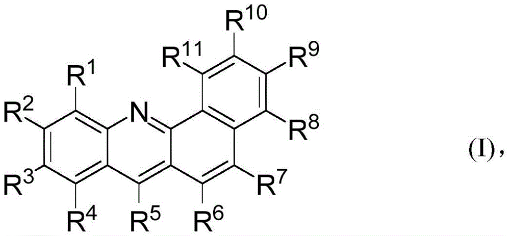
Wherein all R are1To R11All but one are independently selected from H, D, F, substituted or unsubstituted C1To C18Alkyl, substituted or unsubstituted C6To C42Aryl, substituted or unsubstituted C3To C42Heteroaryl, and adjacent radicals R1To R11Can be connected to each other to form a fused ring,
wherein said R1To R11One of the radicals not being selected from the above radicals is a radical G, in which
-said group G comprises an atom a having an electron pair in its p-orbital;
-said group G comprises two 6-membered aryl rings connected to said atom a, wherein each of said two 6-membered aryl rings is connected to said atom a by a single bond, respectively, and wherein said two 6-membered aryl rings connected to said atom a may be connected to each other by a single bond;
-said group G comprises a total of from 12 to 66 carbon atoms;
-said group G is via a single bond or via C6To C18Benzacridine having arylidene groups linked to said compound of formula (I)Moiety wherein said C6To C18The arylidene group is part of the group G; and is
-said group G is unsubstituted or substituted with one or more substituents independently selected from D, F, C1To C18Alkyl radical, C6To C42Aryl radical, C6To C42Heteroaryl, (R)12)2P ═ O, CN or G ', wherein the group G ' is as defined for the group G, except that the group G ' is not attached to the benzacridine moiety of the compound of formula (I), but rather by a single bond or by C6To C18An aromatic subunit linked to the group G, wherein C6To C18The aromatic subunit is part of said group G', with the proviso that said group G passes through said C6To C18In the case where an arylidene group is linked to the benzacridine moiety of the compound of formula (I), it may be linked to C6To C18Substituents of the arylene radical being selected exclusively from C1To C18Alkyl radical, C6To C42Aryl group, (R)12)2P ═ O and CN;
wherein in R other than said group G1To R11In the case that at least one of them is substituted, the corresponding substituent(s) is (are) independently selected from D, F, C1To C18Alkyl radical, C6To C36Aryl radical, C6To C42Heteroaryl, (R)12)2P-O, CN; and is
Wherein R is12Independently selected from C1To C18Alkyl and C6To C24And (4) an aryl group.
The present inventors have surprisingly found that the above-mentioned compounds are suitable for improving the performance, in particular in terms of the working life, of certain layers in organic electronic devices, such as OLEDs.
The p-orbital is a non-hybrid orbital.
In case the group G attached to the benzacridine moiety of said compound of formula (I) is substituted by another group G ', this other group G ' not directly attached to said benzacridine moiety may not comprise another group G ' as a substituent thereof.
According to the invention, the groups G and G' are substantially planar for the atom a, the two 6-membered aryl rings connected to the atom a by single bonds and other groups connected to the atom a.
The two 6-membered aryl rings may contain a ring atom selected from carbon and nitrogen. In one embodiment, the ring atoms of the two 6 membered aryl rings are carbon.
The group G may comprise the following structural unit

The group G may be attached to the benzacridine moiety of the compound of formula (I) at the position indicated by "#".
In the group G, in particular in the structural units described above, the two 6-membered aryl rings may be connected to one another by a single bond.
According to the invention, the radical R1To R11Two (e.g. radicals R) adjacent to each other1And R2) May together form a fused ring. In this connection, the fused ring is R adjacent to the two radicalsnThe rings to which the groups are bonded together form the second ring of the fused ring system. In this way, the two RsnThe two carbon atoms to which the group is bonded are shared by two adjacent rings that are fused to each other. Reference is made to the formula wherein R1And R2Examples of fused rings are formed, and the resulting structure can be shown below, wherein ring X is fused to an adjacent ring Y having a total of two carbon atoms:
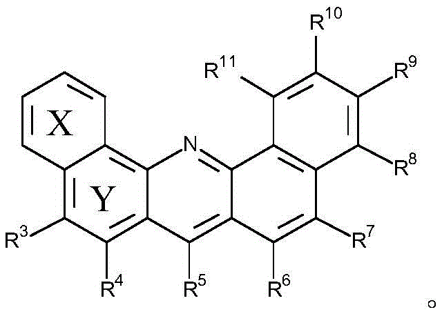
it must be noted, however, that in the above, R1And R2Embodiments that together form a 6-membered aromatic ring (which is a fused ring) are merely exemplary in nature and include other fused rings (e.g., 5-or 7-membered, non-aromatic rings)Family rings, etc.). Preferably, however, there are two adjacent RnThe fused ring formed by the groups is a 6-membered aromatic ring as depicted above.
For the compounds of the invention, the radical R1To R11Is a group G as defined herein. All other radicals R1To R11Variously selected from the groups mentioned above.
The group G comprises an atom a having an electron pair in its p-orbital. The fact that the atom a has an electron pair in its p-orbital creates a chemical structure that is essentially planar for the atom a and the moiety directly attached to the atom a, which means that the three bonds a to #, a to the first aryl group, and a to the second aryl group lie in the same molecular plane within only a few degrees (°) of deviation. The deviation may be 10 ° or 5 ° or <1 °.
This will be exemplified by reference to the following structure:

in the above exemplary structures, the atom a is directly connected to two 6-membered aryl rings (labeled "first aryl" and "second aryl" in the above figures), as required according to the present invention. In the above case where the atom a is a trivalent atom, such as a nitrogen atom N, the angle between the bond connecting the first aryl group to atom a and the bond connecting the second aryl group to group a is about 120 °, such as 110 ° to 120 °, or 115 ° to 120 °, or 119 ° to 120 °. The same is true for the bond # to the atom A and the corresponding bond A to the first aryl group, the corresponding second aryl group.
The two 6-membered aryl rings connected to the atom a may not be connected to each other, or may be connected to each other by a single bond. In the first case (not connected), the corresponding structure may be as described above.
In the case where the two 6-membered aryl rings are connected to each other by a single bond, the group G or G' may comprise the following structure:

said group G may be bonded at position "#" either by a single bond or by C6To C18(ii) Arylidene attachment to the benzacridine moiety of said compound of formula (I)

Said C is6To C18The aromatic subunit (if present) is part of the group G. That is, where the group G is substituted, the substituent attached to the group G may be attached to C6To C18An aromatic subunit moiety, said C6To C18An arylidene moiety connects the group G to the benzacridine moiety of the compound of formula (I).
The group G comprises only one atom a. However, in case said group G is substituted by another group G' as defined herein, said compound of general formula (I) may comprise another atom a instead of said group G. The group G' cannot be linked to C6To C18Aryl subunit of, said C6To C18An arylidene group as part of the group G and linking the group G to the benzacridine moiety of the compound of formula (I).
In the compound of formula (I), the group G may comprise 1 to 5 heteroatoms selected from N, S and O. In this way, the ability of the compound of formula (I) to improve the working life of the organic electronic device comprising it is further improved.
In the compound of formula (I), the atom a may be selected from N, S and O. In this way, the ability of the compound of formula (I) to improve the working life of the organic electronic device comprising it is further improved.
In the compound of formula (I), the atom a may be N. In this way, the ability of the compound of formula (I) to improve the working life of the organic electronic device comprising it is further improved.
In the compound of formula (I), the group G may comprise the atom a and the two 6-membered aryl rings connected to the atom a in the form of a diarylamino group or in the form of a carbazolyl group. In this way, the ability of the compound of formula (I) to improve the operating lifetime of an organic electronic device comprising it is further improved.
In the compound of formula (I), the total number of aromatic rings included in the compound of formula (I) may be 6 to 21. In this way, the ability of the compound of formula (I) to improve the working life of the organic electronic device comprising it is further improved.
In the compound of the formula (I), R1And R2Or R2And R3Or R3And R4May together form an aryl ring. In this connection, the abovementioned pairs of adjacent radicals RnOnly one pair of which forms a fused ring. The fused rings formed in this way are those mentioned above. In this way, the ability of the compound of formula (I) to improve the working life of the organic electronic device comprising it is further improved.
In one embodiment, R1And R2Or R3And R4Fused rings may be formed. Preferably, R1And R2Fused rings may be formed.
In the compound of the formula (I), the compound represented by R1And R2Or R2And R3Or R3And R4The fused ring formed may be C6-an aryl ring. In this way, the ability of the compound of formula (I) to improve the working life of the organic electronic device comprising it is further improved.
In the compounds of formula (I), the group G may be replaced by unsubstituted C6To C18An arylidene group is attached to the benzacridine moiety of the compound of formula (I). In this regard, the group G is attached to the unsubstituted C of the benzacridine moiety6To C18The arylene group can be phenyleneAnd (4) a base. In this way, the ability of the compound of formula (I) to improve the working life of the organic electronic device comprising it is further improved.
In the compounds of the general formula (I), R5Or R10May be said group G. In other words, preferably the group G is at R5Or R10(ii) a benzacridine moiety attached at a position to said compound of formula (I). In this way, the ability of the compound of formula (I) to improve the working life of the organic electronic device comprising it is further improved.
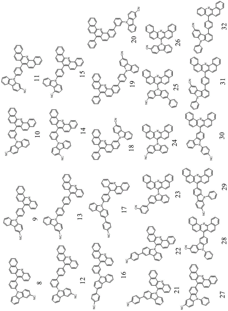
In a very preferred embodiment, the compound of formula (I) is one selected from the group consisting of,

in one embodiment, the compound of formula (I) has an energy gap LUMO-HOMO below 3.89 eV.
The object is also achieved by an organic electronic device comprising an organic semiconductor layer, wherein the organic semiconductor layer comprises a compound of general formula (I) as described herein.
The organic electronic device may further comprise a first electrode and a second electrode, wherein the organic semiconductor layer is disposed between the first electrode and the second electrode.
In the organic electronic device, the organic semiconductor layer may be a light emitting layer. That is, according to one embodiment of the present invention, the organic electronic device includes the compound of formula (I) in a light emitting layer thereof.
In another embodiment, the organic semiconductor layer is a hole blocking layer. That is, in one embodiment of the present invention, the organic electronic device includes the compound of formula (I) in a hole blocking layer thereof.
In this regard, the hole blocking layer may not include a dopant or an additive.
In another embodiment, the organic semiconductor layer is an electron transport layer. That is, in this embodiment, the organic electronic device comprises the compound of formula (I) in its electron transport layer.
In this connection, the electron transport layer may also comprise (in addition to the compound of formula (I)) dopants or additives.
In this regard, suitable additives or dopants may be n-type additives or n-type dopants, such as LiQ, rare earth metals, alkali metals, alkaline earth metals, borates (CAS 14728-62-2), phenolates (e.g., CAS 1440864-50-5), phosphinimines (e.g., CAS 51870-56-5), guanidines (e.g., CAS 1623748-16-2), metal complexes as disclosed in US2009212280, heterocyclic compounds as disclosed in US2007252140, and the like.
In the organic electronic device, the organic semiconductor layer may further include at least one second compound in addition to the compound of formula (I). In this regard, the at least one second compound may be a metal, a metal salt, a metal complex, a heterocyclic compound disclosed in US2007252140, an organic or metal organic emitter compound or a mixture thereof. The metal complex may be an organic alkali metal complex or a complex as disclosed in US 2009212280. The organic alkali metal complex may be an alkali metal borate and/or phenoxide and/or lithium 8-hydroxyquinoline.
The object is also achieved by a display device comprising an organic electronic device as defined herein.
The object is also achieved by a lighting device comprising an organic electronic device as defined herein.
The structure of the embodiment section of the present application is most preferable.
Other layers
According to the invention, the organic electronic device may comprise further layers in addition to the layers already mentioned above. Exemplary embodiments of the respective layers are described below:
substrate
The substrate may be any substrate commonly used in the manufacture of electronic devices such as organic light emitting diodes. If light is emitted through the substrate, the substrate should be a transparent or translucent material, such as a glass substrate or a transparent plastic substrate. If light is emitted through the top surface, the substrate may be both transparent and opaque materials, such as a glass substrate, a plastic substrate, a metal substrate, or a silicon substrate.
Anode
Either one of the first electrode or the second electrode included in the organic electronic device of the present invention may be an anode. The anode may be formed by depositing or sputtering the material used to form the anode. The material used to form the anode may be a high work function material to facilitate hole injection. The anode material may also be selected from low work function materials (i.e., aluminum). The anode may be a transparent or reflective electrode. Transparent conductive oxides such as Indium Tin Oxide (ITO), Indium Zinc Oxide (IZO), tin dioxide (SnO)2) Zinc aluminum oxide (AlZO) and zinc oxide (ZnO) may be used to form the anode. The anode may also be formed using a metal, typically silver (Ag), gold (Au), or a metal alloy.
Hole injection layer
The Hole Injection Layer (HIL) may be formed on the anode by vacuum deposition, spin coating, printing, casting, slit coating, Langmuir-blodgett (lb) deposition, or the like. When the HIL is formed using vacuum deposition, the deposition conditions may vary depending on the compound used to form the HIL and the desired structural and thermal properties of the HIL. However, in general, the conditions for vacuum deposition may include a deposition temperature of 100 ℃ to 500 ℃,10 ℃-8To 10-3A pressure of torr (1 torr equals 133.322Pa) and a deposition rate of 0.1 to 10 nm/sec.
When the HIL is formed using spin coating or printing, the coating conditions may vary according to the compound used to form the HIL and the desired structural and thermal properties of the HIL. For example, the coating conditions may include a coating speed of about 2000rpm to about 5000rpm and a heat treatment temperature of about 80 ℃ to about 200 ℃. After the coating is performed, the solvent is removed by heat treatment.
The HIL may be formed from any compound commonly used to form HILs. Examples of compounds that may be used to form the HIL include phthalocyanine compounds such as copper phthalocyanine (CuPc), 4' -tris (3-methylphenylphenylamino) triphenylamine (m-MTDATA), TDATA, 2T-NATA, polyaniline/dodecylbenzene sulfonic acid (Pani/DBSA), poly (3, 4-ethylenedioxythiophene) poly (4-styrenesulfonate) (PEDOT/PSS), polyaniline/camphorsulfonic acid (Pani/CSA), and polyaniline/poly (4-styrenesulfonate) (PANI/PSS).
The HIL may contain or consist of a p-type dopant, and the p-type dopant may be selected from tetrafluoro-tetracyanoquinodimethane (F4TCNQ), 2' - (perfluoronaphthalene-2, 6-diylidene) dipropionarylonitrile or 2,2',2 "- (cyclopropane-1, 2, 3-triylidene) tris (2- (p-cyanotetrafluorophenyl) acetonitrile), but is not limited thereto the HIL may be selected from hole transport matrix compounds doped with a p-type dopant typical examples of known doped hole transport materials are copper phthalocyanine (CuPc) having a HOMO energy level of about-5.2 eV, tetrafluoro-tetracyanoquinodimethane (F4TCNQ) having a LUMO energy level of about-5.2 eV, zinc phthalocyanine (ZnPc) doped with F4TCNQ (HOMO ═ 5.2eV), α -NPD (N, N ' -bis (naphthalene-1-yl) -N, N ' -bis (phenyl) -benzidine) doped with F4TCNQ, or from dipropyl-2, 2' - (perfluoronaphthalene-1, 6-diylidene) having a concentration of preferably from about 10% by weight to α% by weight of the dopant.
The HIL may have a thickness in a range from about 1nm to about 100nm, for example, from about 1nm to about 25 nm. When the thickness of the HIL is within this range, the HIL may have excellent hole injection characteristics without substantial deterioration of driving voltage.
Hole transport layer
A Hole Transport Layer (HTL) may be formed on the HIL by vacuum deposition, spin coating, slit coating, printing, casting, Langmuir-blodgett (lb) deposition, or the like. When the HTL is formed by vacuum deposition or spin coating, conditions for deposition and coating may be similar to those for forming the HIL. However, the conditions for vacuum or solution deposition may vary depending on the compound used to form the HTL.
The HTL may be formed of any compound commonly used to form HTLs, compounds that may be suitably used are disclosed in, for example, Yasuhiko Shirota and Hiroshi Kageyama, chem.rev.2007,107,953-1010, and incorporated herein by reference examples of compounds that may be used to form HTLs are carbazole derivatives such as N-phenylcarbazole or polyvinylcarbazole, benzidine derivatives such as N, N '-bis (3-methylphenyl) -N, N' -diphenyl- [1, 1-biphenyl ] -4,4 '-diamine (TPD) or N, N' -bis (naphthalen-1-yl) -N, N '-diphenylbenzidine (α -NPD), and triphenylamine-based compounds such as 4,4',4 ″ -tris (N-carbazolyl) triphenylamine (TCTA), among which TCTA may transport holes and inhibit exciton diffusion into EML.
The thickness of the HTL may range from about 5nm to about 250nm, preferably from about 10nm to about 200nm, more preferably from about 20nm to about 190nm, more preferably from about 40nm to about 180nm, more preferably from about 60nm to about 170nm, more preferably from about 80nm to about 160nm, more preferably from about 100nm to about 160nm, more preferably from about 120nm to about 140 nm.
When the thickness of the HTL is within this range, the HTL may have excellent hole transport characteristics without substantial deterioration of driving voltage.
Electron blocking layer
The function of the Electron Blocking Layer (EBL) is to prevent electrons from being transferred from the light emitting layer to the hole transport layer and thus confine electrons to the light emitting layer. Thereby improving efficiency, operating voltage, and/or lifetime. Typically, the electron blocking layer comprises a triarylamine compound. The triarylamine compound may have a LUMO level closer to a vacuum level than a LUMO level of the hole transport layer. The electron blocking layer may have a HOMO energy level that is further from a vacuum energy level than a HOMO energy level of the hole transport layer. The thickness of the electron blocking layer may be selected between 2 and 20 nm.
The electron blocking layer can also be described as a triplet-controlling layer if it has a high triplet energy level.
The function of the triplet-controlling layer is to reduce quenching of triplet states in the case of using a green or blue phosphorescent light-emitting layer. Thereby, more efficient light emission from the phosphorescent light-emitting layer can be achieved. The triplet-controlling layer is selected from compounds having a triplet energy level higher than that of a phosphorescent emitter in an adjacent light-emitting layer. Suitable compounds for the triplet-controlling layer, in particular triarylamine compounds, are described in EP 2722908 a 1.
Luminous layer (EML)
The EML may be formed on the HTL by vacuum deposition, spin coating, slit coating, printing, casting, LB deposition, or the like. When the EML is formed using vacuum deposition or spin coating, conditions for deposition and coating may be similar to those for forming the HIL. However, conditions for deposition and coating may vary depending on the compound used to form the EML.
The light emitting layer may comprise a compound of formula (I).
The EML may be formed from a combination of a host material and an emitter dopant. The EML may comprise a single host material or multiple host materials. The EML may comprise a single emitter dopant or multiple emitter dopants. Examples of such host materials are Alq3, 4' -N, N ' -dicarbazole-biphenyl (CBP), poly (N-vinylcarbazole) (PVK), 9, 10-bis (naphthalen-2-yl) Anthracene (ADN), 4',4 ″ -tris (carbazol-9-yl) -triphenylamine (TCTA), 1,3, 5-tris (N-phenylbenzimidazol-2-yl) benzene (TPBI), 3-tert-butyl-9, 10-bis-2-naphthylanthracene (TBADN), bis (styryl) arylidene (DSA), bis (2- (2-hydroxyphenyl) benzothiazole) zinc (zn (btz))2) Or a compound of formula (I).
Where the EML comprises a plurality of host materials to form a host mixture, the amount of each host material in the mixture of host materials may vary between 0.01 to 99.99 parts by weight.
The emitter dopant may be a phosphorescent or fluorescent emitter. Phosphorescent emitters and emitters that emit by a Thermally Activated Delayed Fluorescence (TADF) mechanism are preferred due to their higher efficiency. The luminophores may be small molecules or polymers.
Examples of red emitter dopants are PtOEP, Ir (piq)3And Btp2lr (acac), but is not limited thereto. These compounds are phosphorescent emitters, however red fluorescent emitter dopants may also be used.
Examples of green phosphorescent emitter dopants are Ir (ppy)3(ppy. phenylpyridine), Ir (ppy)2(acac)、Ir(mpyp)3。
An example of a blue phosphorescent emitter dopant is F2Irpic、(F2ppy)2Ir (tmd) and Ir (dfppz)3And a trifluorofluorene. 4' -bis (4-diphenylaminostyryl) biphenyl (DPAVBi), 2,5,8, 11-tetra-tert-butylperylene (TBPe) are examples of blue fluorescent emitter dopants.
The amount of the emitter dopant may be in the range of about 0.01 to about 50 parts by weight, based on 100 parts by weight of the host or the host mixture. Alternatively, the light-emitting layer may be composed of a light-emitting polymer. The EML may have a thickness of about 10nm to about 100nm, for example about 20nm to about 60 nm. When the thickness of the EML is within this range, the EML may have excellent light emission without substantial deterioration of driving voltage.
Hole Blocking Layer (HBL)
A Hole Blocking Layer (HBL) may be formed on the EML by using vacuum deposition, spin coating, slit coating, printing, casting, LB deposition, etc. in order to prevent holes from diffusing into the ETL. When the EML includes a phosphorescent dopant, the HBL may also have a triplet exciton blocking function. The hole blocking layer may be the organic semiconductor layer of the present invention, which contains the compound of the present invention represented by the general formula (I) as defined above, or which is composed of the compound represented by the general formula (I).
The HBL may be the layer (or one of a plurality of layers) comprising the compound of formula (I).
The HBL may also be referred to as an auxiliary ETL or a-ETL.
When the HBL is formed using vacuum deposition or spin coating, conditions for deposition and coating may be similar to those for forming the HIL. However, forThe conditions for deposition and coating may vary depending on the compound used to form the HBL. Any compound commonly used to form HBLs may be used. Examples of compounds useful for forming the HBL include Oxadiazole derivatives, triazine derivatives, triazole derivatives, and phenanthroline derivatives.
The HBL may have a thickness in the range of about 5nm to about 100nm, for example about 10nm to about 30 nm. When the thickness of the HBL is within this range, the HBL may have excellent hole blocking performance without substantial deterioration of driving voltage.
Electronic Transmission Layer (ETL)
The OLED according to the present invention may comprise an Electron Transport Layer (ETL). According to the present invention, the electron transport layer may be the organic semiconductor layer of the present invention comprising the compound of the present invention represented by the general formula (I) as defined above. In one embodiment, the ETL may be comprised of a compound of formula (I).
According to various embodiments, the OLED may comprise an electron transport layer or an electron transport layer stack structure comprising at least one first electron transport layer and at least one second electron transport layer.
By appropriately adjusting the energy level of a specific layer of the ETL, the injection and transport of electrons can be controlled, and holes can be efficiently blocked. Therefore, the OLED may have a long lifetime.
The electron transport layer of the organic electronic device may comprise a compound represented by the general formula (I) as defined above as an organic Electron Transport Matrix (ETM) material. In addition to the compound represented by the general formula (I), the electron transport layer may further include other ETM materials known in the art. Likewise, the electron transport layer may contain the compound represented by the general formula (I) as the only electron transport host material. In the case where the organic electronic device of the present invention includes more than one electron transport layer, the compound represented by the general formula (I) may be included in only one of the electron transport layers, in more than one of the electron transport layers, or in all of the electron transport layers. According to the invention, the electron transport layer may comprise, in addition to the ETM material, at least one additive as defined herein.
In addition, the electron transport layer may include one or more n-type dopants. The additive may be an n-type dopant. The additive may be an alkali metal, an alkali metal compound, an alkaline earth metal compound, a transition metal compound, or a rare earth element metal. In another embodiment, the metal may be one selected from the group consisting of Li, Na, K, Rb, Cs, Mg, Ca, Sr, Ba, La, Ce, Sm, Eu, Tb, Dy and Yb. In another embodiment, the n-type dopant may be one selected from Cs, K, Rb, Mg, Na, Ca, Sr, Eu and Yb. In one embodiment, the alkali metal compound may be lithium 8-hydroxyquinoline (LiQ), lithium tetrakis (1H-pyrazol-1-yl) borate, or lithium 2- (diphenylphosphoryl) phenoxide. The compound suitable for ETM, which may be used in addition to the compound of the present invention represented by the general formula (I) as defined above, is not particularly limited. In one embodiment, the electron transport matrix compound is comprised of covalently bonded atoms. Preferably, the electron transport matrix compound comprises a conjugated system of at least 6, more preferably at least 10 delocalized electrons. In one embodiment, the conjugated system of delocalized electrons may be comprised in an aromatic or heteroaromatic moiety, as disclosed for example in documents EP 1970371 a1 or WO 2013/079217 a 1.
Electron Injection Layer (EIL)
An optional EIL, which may facilitate injection of electrons from the cathode, may be formed on the ETL, preferably directly on the electron transport layer. Examples of materials for forming the EIL include lithium 8-hydroxyquinoline (LiQ), LiF, NaCl, CsF, Li, which are known in the art2O, BaO, Ca, Ba, Yb, Mg. Deposition and coating conditions for forming the EIL are similar to those for forming the HIL, but the deposition and coating conditions may be according to a material used to form the EILThe material varies. The EIL may be an organic semiconductor layer comprising the compound of formula (I).
The EIL may have a thickness in a range from about 0.1nm to about 10nm, for example, in a range from about 0.5nm to about 9 nm. When the thickness of the EIL is within this range, the EIL may have satisfactory electron injection performance without substantial deterioration of the driving voltage.
Cathode electrode
The cathode is formed on the EIL, if present. The cathode may be formed of a metal, an alloy, a conductive compound, or a mixture thereof. The cathode may have a low work function. For example, the cathode may be formed of lithium (Li), magnesium (Mg), aluminum (Al) -lithium (Li), calcium (Ca), barium (Ba), ytterbium (Yb), magnesium (Mg) -indium (In), magnesium (Mg) -silver (Ag), or the like. Alternatively, the cathode may be formed of a transparent conductive oxide such as ITO or IZO.
The cathode may have a thickness in the range of about 5nm to about 1000nm, for example in the range of about 10nm to about 100 nm. When the cathode has a thickness in the range of about 5nm to about 50nm, the cathode may be transparent or translucent even if it is formed of a metal or a metal alloy.
It should be understood that the cathode is not part of the electron injection layer or electron transport layer.
Charge generation layer
The Charge Generation Layer (CGL) may include p-type and n-type layers. An intermediate layer may be disposed between the p-type layer and the n-type layer. The CGL may include the compound represented by the general formula (I).
Typically, the charge generation layer is a p-n junction that joins an n-type charge generation layer (electron generation layer) and a hole generation layer. The n-side of the p-n junction generates electrons and injects them into a layer adjacent to the p-n junction in a direction towards the anode. Similarly, the p-side of the p-n junction generates holes and injects them into the layer adjacent to the p-n junction in a direction towards the cathode.
The charge generating layer can be used in a tandem device, such as a tandem OLED comprising two or more light emitting layers between two electrodes. In a tandem OLED comprising two light emitting layers, the n-type charge generation layer provides electrons to a first light emitting layer disposed near an anode, and the hole generation layer provides holes to a second light emitting layer disposed between the first light emitting layer and a cathode.
Suitable host materials for the hole generating layer may be materials conventionally used as hole injection and/or hole transport host materials. In addition, the p-type dopant used for the hole generation layer may use a conventional material. For example, the p-type dopant may be selected from tetrafluoro-7, 7,8, 8-tetracyanoquinodimethane (F4-TCNQ), tetracyanoquinodimethane derivatives, limonene derivatives, iodine, FeCl3、FeF3And SbCl5One kind of (1). Further, the host material may be one selected from N, N ' -di (naphthalene-1-yl) -N, N-diphenyl-benzidine (NPB), N ' -diphenyl-N, N ' -bis (3-methylphenyl) -1, 1-biphenyl-4, 4' -diamine (TPD), and N, N ' -tetranaphthyl-benzidine (TNB). The p-type charge generation layer may be composed of CNHAT.
The n-type charge generation layer may be a layer containing the compound of formula (I). The n-type charge generation layer may be a layer of a pure n-type dopant, such as an electropositive metal, or may be composed of an organic host material doped with an n-type dopant. In one embodiment, the n-type dopant may be an alkali metal, an alkali metal compound, an alkaline earth metal compound, a transition metal compound, or a rare earth metal. In another embodiment, the metal may be one selected from the group consisting of Li, Na, K, Rb, Cs, Mg, Ca, Sr, Ba, La, Ce, Sm, Eu, Tb, Dy and Yb. More specifically, the n-type dopant may be one selected from Cs, K, Rb, Mg, Na, Ca, Sr, Eu, and Yb. Suitable host materials for the electron generation layer may be materials conventionally used as host materials for electron injection or electron transport layers. The matrix material may be, for example, one selected from triazine compounds, hydroxyquinoline derivatives such as tris (8-hydroxyquinoline) aluminum, benzoxazole derivatives, and silacore derivatives.
The hole generation layer is disposed in direct contact with the n-type charge generation layer.
Organic Light Emitting Diode (OLED)
The organic electronic device according to the present invention may be an organic light emitting device.
According to an aspect of the present invention, there is provided an Organic Light Emitting Diode (OLED) including: the organic light emitting diode comprises a substrate, an anode, a hole injection layer, a hole transport layer, a light emitting layer, an organic semiconductor layer containing or consisting of a compound of formula (I), and a cathode, wherein the anode, the hole injection layer, the hole transport layer, the light emitting layer and the organic semiconductor layer are formed on the substrate.
According to another aspect of the present invention, there is provided an OLED comprising: the organic light emitting diode comprises a substrate, an anode, a hole injection layer, a hole transport layer, an electron blocking layer, a light emitting layer, a hole blocking layer, an organic semiconductor layer containing or consisting of a compound of formula (I), and a cathode, wherein the anode, the hole injection layer, the hole transport layer, the electron blocking layer, the light emitting layer and the hole blocking layer are formed on the substrate.
According to another aspect of the present invention, there is provided an OLED comprising: a substrate, an anode formed on the substrate, a hole injection layer, a hole transport layer, an electron blocking layer, a light emitting layer, a hole blocking layer, an organic semiconductor layer comprising or consisting of a compound of formula (I), an electron injection layer, and a cathode.
According to various embodiments of the present invention, there may be provided OLED layers arranged between the above-mentioned layers, on the substrate or on the top electrode.
According to one aspect, the OLED may comprise the following layer structure: a substrate disposed adjacent to an anode, the anode disposed adjacent to a first hole injection layer, the first hole injection layer disposed adjacent to a first hole transport layer, the first hole transport layer disposed adjacent to a first electron blocking layer, the first electron blocking layer disposed adjacent to a first light emitting layer, the first light emitting layer disposed adjacent to a first electron transport layer, the first electron transport layer disposed adjacent to an n-type charge generation layer, the n-type charge generation layer disposed adjacent to a hole generation layer, the hole generation layer disposed adjacent to a second hole transport layer, the second hole transport layer disposed adjacent to a second electron blocking layer, the second electron blocking layer disposed adjacent to a second light emitting layer, an optional electron transport layer and/or an optional electron injection layer disposed between the second light emitting layer and a cathode.
The organic semiconductor layer according to the present invention may be a light emitting layer, a hole blocking layer, an electron transport layer, a first electron transport layer, an n-type charge generation layer, and/or a second electron transport layer.
For example, the OLED (10) according to FIG. 2 can be formed by a method wherein
On the substrate (110), an anode (120), a hole injection layer (130), a hole transport layer (140), an electron blocking layer (145), a light emitting layer (150), a hole blocking layer (155), an electron transport layer (160), an electron injection layer (180), and a cathode (190) are sequentially formed.
Organic electronic device
The organic electronic device according to the invention comprises an organic semiconductor layer which contains or consists of a compound according to formula (I).
An organic electronic device according to an embodiment may include a substrate, an anode layer, an organic semiconductor layer including or consisting of a compound of formula (I), and a cathode layer.
An organic electronic device according to one embodiment comprises at least one organic semiconductor layer containing or consisting of at least one compound of formula (I), at least one anode layer, at least one cathode layer and at least one light-emitting layer, wherein the organic semiconductor layer is preferably arranged between the light-emitting layer and the cathode layer.
An Organic Light Emitting Diode (OLED) according to the present invention may include an anode, a Hole Transport Layer (HTL), an emission layer (EML), an Electron Transport Layer (ETL) including at least one compound of formula (I), and a cathode, which are sequentially stacked on a substrate. In this regard, the HTL, EML, and ETL are thin films formed of organic compounds.
The organic electronic device according to an embodiment may be a light emitting device, a thin film transistor, a battery pack, a display device, or a photovoltaic cell, preferably a light emitting device.
According to an aspect of the present invention, there is provided a method of manufacturing an organic electronic device, the method using:
-at least one deposition source, preferably two deposition sources, more preferably at least three deposition sources.
Suitable methods for deposition include:
-deposition by vacuum thermal evaporation;
-deposition by solution processing, preferably said processing is selected from spin coating, printing, casting; and/or
Slit coating.
According to various embodiments of the present invention, there is provided a method using:
-a first deposition source to release a compound of formula (I) according to the invention, and
-a second deposition source to release a metal, metal complex, organometallic compound, metal salt or alkali or alkaline earth metal complex, or organic alkali or alkaline earth metal complex, or lithium 8-hydroxyquinoline or alkali metal borate;
the method comprises the step of forming the organic semiconductor layer, thereby for an Organic Light Emitting Diode (OLED):
-the organic semiconductor layer is formed by: releasing a compound of formula (I) according to the invention from the first deposition source and releasing a metal, metal complex, organometallic compound, metal salt or alkali metal or alkaline earth metal complex or organic alkali metal or alkaline earth metal complex or lithium 8-hydroxyquinoline or alkali metal borate from the second deposition source.
According to various embodiments of the present invention, the method may further comprise forming a light emitting layer on the anode, and forming at least one layer between the anode and the first electron transporting layer, the at least one layer selected from forming a hole injecting layer, forming a hole transporting layer, or forming a hole blocking layer.
According to various embodiments of the present invention, the method may further comprise a step for forming an Organic Light Emitting Diode (OLED), wherein:
-forming a first anode on a substrate,
-forming a light emitting layer on the first anode,
-forming an electron transport layer stack structure over the light emitting layer, optionally forming a hole blocking layer over the light emitting layer and forming an organic semiconductor layer,
-finally forming a cathode,
-forming an optional hole injection layer, a hole transport layer and a hole blocking layer in that order between the first anode and the light emitting layer,
-forming an optional electron injection layer between the organic semiconductor layer and the cathode.
According to various embodiments of the present invention, the method may further include forming an electron injection layer on the organic semiconductor layer. However, according to various embodiments of the OLED of the present invention, the OLED may not comprise an electron injection layer.
According to various embodiments, the OLED may have the following layer structure, wherein the layers have the following order:
an anode, a hole-injecting layer, a first hole-transporting layer, a second hole-transporting layer, a light-emitting layer, optionally a hole-blocking layer, an organic semiconductor layer comprising a compound of formula (I) according to the invention, optionally an electron-injecting layer and a cathode, or
An anode, a hole-injecting layer, a first hole-transporting layer, a second hole-transporting layer, an organic semiconductor layer comprising a compound of formula (I) according to the invention, an optional hole-blocking layer, a first electron-transporting layer, an optional electron-injecting layer and a cathode, or
An anode, a hole injection layer, a first hole transport layer, a second hole transport layer, a light-emitting layer, an organic semiconductor layer comprising a compound of formula (I) according to the invention, a first electron transport layer, optionally an electron injection layer and a cathode.
According to another aspect of the present invention, there is provided an electronic device comprising at least one organic light emitting device according to any of the embodiments described throughout the present application, preferably an organic light emitting diode in one of the embodiments described throughout the present application. More preferably, the electronic device is a display device.
In one embodiment, the organic electronic device according to the present invention comprising an organic semiconductor layer comprising or consisting of a compound according to formula (I) may further comprise a layer comprising an radialene compound and/or a quinodimethane compound.
In one embodiment, the radialene compound and/or the quinodimethane compound may be substituted with one or more halogen atoms and/or one or more electron withdrawing groups. The electron-withdrawing group may be selected from a nitrile group, a haloalkyl group, alternatively a perhaloalkyl group, alternatively a perfluoroalkyl group. Other examples of electron withdrawing groups may be acyl, sulfonyl or phosphoryl groups.
Alternatively, the acyl, sulfonyl and/or phosphoryl groups may comprise halogenated and/or perhalogenated hydrocarbon groups. In one embodiment, the perhalogenated hydrocarbon group may be a perfluorinated hydrocarbon group. Examples of perfluoroalkyl groups may be perfluoromethyl, perfluoroethyl, perfluoropropyl, perfluoroisopropyl, perfluorobutyl, perfluorophenyl, perfluorotolyl; examples of the sulfonyl group containing a halogenated hydrocarbon group may be trifluoromethylsulfonyl group, pentafluoroethylsulfonyl group, pentafluorophenylsulfonyl group, heptafluoropropylsulfonyl group, nonafluorobutylsulfonyl group and the like.
In one embodiment, the limonene and/or quinodimethane compounds may be included in the hole injection, hole transport, and/or hole generation layers.
In one embodiment, the radialene compound may have formula (XX), and/or the quinodimethane compound may have formula (XXIa) or (XXIb):

wherein R is1、R2、R3、R4、R5、R6、R7、R8、R11、R12、R15、R16、R20、R21Is independently selected from the electron withdrawing groups mentioned above, and R9、R10、R13、R14、R17、R18、R19、R22、R23And R24Independently selected from H, halogen and electron withdrawing groups as mentioned above.
Hereinafter, embodiments will be described in more detail with reference to examples. However, the present disclosure is not limited to the following embodiments. Reference will now be made in detail to the exemplary aspects.
Details and definitions of the invention
The term "fused ring" is used herein to refer to a bonding situation in which two adjacent R' s1To R11For example R1And R2Or R2And R3Or R3And R4Together form a ring fused to the remainder of the structure having formula (I).
In the present specification, when a definition is not otherwise provided, "alkyl" may refer to an aliphatic hydrocarbon group. Alkyl may refer to "saturated alkyl" without any double or triple bonds. As used herein, the term "alkyl" will encompass straight chain as well as branched and cyclic alkyl groups. E.g. C3The alkyl group may be chosen from n-propyl and isopropyl. Likewise, C4Alkyl encompasses n-butyl, sec-butyl and tert-butyl. Likewise, C6Alkyl encompasses n-hexyl and cyclohexyl.
CnThe subscript number n in (a) relates to the total number of carbon atoms in the corresponding alkyl, aryl, heteroaryl or aryl group.
When used herein, the term "aryl" or "arylidene" will encompass phenyl (C)6Aryl), fused aromatic compounds such as naphthalene, anthracene, phenanthrene, tetracene, and the like. Also contemplated are biphenyls and oligo-or poly-benzenes such as terphenyls and the like. Any other aromatic hydrocarbon substituent such as fluorenyl and the like is also contemplated. "Arylene" and the corresponding "heteroarene" refer to a group to which two additional moieties are attached. In the present specification, the term "aryl" or "arylidene" mayRefers to a group that contains at least one aromatic hydrocarbon moiety, and all elements of the aromatic hydrocarbon moiety may have p orbitals that form conjugates, such as phenyl, naphthyl, anthryl, phenanthryl, pyrenyl, fluorenyl, and the like. The aryl or aryl subunit may include a monocyclic or fused ring polycyclic (i.e., rings that share adjacent pairs of carbon atoms) functionality.
As used herein, the term "heteroaryl" refers to an aryl group in which at least one carbon atom is replaced by a heteroatom preferably selected from N, O, S, B or Si.
CnThe subscript number n in heteroaryl refers only to the number of carbon atoms not including the number of heteroatoms. In this context, C is evident3Heteroarylenes are aromatic compounds containing 3 carbon atoms, e.g. pyrazoles, imidazoles, and combinations thereof, Oxazoles, thiazoles, and the like.
The term "heteroaryl" may refer to an aromatic heterocyclic ring having at least one heteroatom, and all elements of the heteroaromatic hydrocarbon moiety may have a p-orbital forming a conjugate. The heteroatom may be selected from N, O, S, B, Si, P, Se, preferably from N, O and S. The heteroaryl subunit ring may comprise at least 1 to 3 heteroatoms. Preferably, the heteroaryl subunit ring may comprise at least 1 to 3 heteroatoms each selected from N, S and/or O.
The term "heteroaryl" as used herein is intended to encompass pyridine, quinoline, quinazoline, pyridine, triazine, benzimidazole, benzothiazole, benzo [4,5 ]]Thieno [3,2-d]Pyrimidines, carbazoles, xanthenes, thiophenes Oxazines, benzacridine, dibenzoacridine, and the like.
In the present specification, a single bond means a direct bond.
As used herein, the term "fluoro" refers to a hydrocarbon group in which at least one hydrogen atom contained in the hydrocarbon group is replaced with a fluorine atom. Fluoro groups in which all hydrogen atoms are replaced by fluorine atoms are referred to as perfluoro groups and are referred to with the term "perfluoro" in particular.
According to the present invention, a group is "substituted" by another group if one of the hydrogen atoms contained in the group is replaced by another group, wherein the other group is a substituent.
According to the invention, the expression "between" does not exclude the presence of other layers which may be arranged between said one layer and one of said other two layers, for a layer between said other two layers. According to the invention, for two layers in direct contact with each other, the expression "in direct contact" means that no other layer is arranged between those two layers. A layer deposited on top of another layer is considered to be in direct contact with that layer.
The compounds mentioned in the experimental section are most preferred for the organic semiconductor layer of the invention and for the compounds of the invention.
The organic electronic device of the present invention may be an organic electroluminescent device (OLED), an organic photovoltaic device (OPV), a lighting fixture or an Organic Field Effect Transistor (OFET). The illumination device may be any device for illumination, radiation, signaling or projection. They are classified accordingly as illumination, radiation, signal and projection devices. The lighting device is generally composed of: the system includes an optical radiation source, a means of transmitting the radiation flux in a desired direction into space, and a housing that connects the components into a single device and protects the radiation source and light transmission system from damage and environmental influences.
According to another aspect, the organic electroluminescent device according to the invention may comprise more than one light-emitting layer, preferably two or three light-emitting layers. OLEDs comprising more than one light emitting layer are also described as tandem OLEDs or stacked OLEDs.
The organic electroluminescent device (OLED) may be a bottom emitting or top emitting device.
Another aspect relates to an apparatus comprising at least one organic electroluminescent device (OLED).
The device comprising the organic light emitting diode is, for example, a display or a lighting panel.
In the present invention, terms will be defined below, unless a different definition is given in the claims or elsewhere in this specification, these definitions shall prevail.
In the context of the present specification, the terms "different" or "difference" in relation to the matrix materials mean that the matrix materials differ in their structural formula.
The terms "OLED" and "organic light emitting diode" are used simultaneously and have the same meaning. As used herein, the term "organic electroluminescent device" may encompass both organic light emitting diodes and Organic Light Emitting Transistors (OLETs).
As used herein, "weight percent," "wt. -%", "percent by weight," "wt%", "parts by weight," and variations thereof, means that the composition, component, substance, or agent is expressed as the weight of that component, substance, or agent of the corresponding electron transport layer divided by the total weight of the corresponding electron transport layer and multiplied by 100. It is to be understood that the amount of the total weight percent of all components, species and agents of the respective electron transport and electron injection layers is selected such that it does not exceed 100 weight percent.
As used herein, "volume percent," vol- "," percent by volume, "" vol% "," and variations thereof refer to a composition, component, substance, or reagent as the volume of that component, substance, or reagent of the corresponding electron transport layer divided by the total volume of the corresponding electron transport layer and multiplied by 100. It should be understood that the amount of the total volume percentage of all components, substances and agents of the cathode layer is selected such that it does not exceed 100 volume%.
All numerical values herein are assumed to be modified by the term "about," whether or not explicitly indicated. As used herein, the term "about" refers to variations that can occur in numerical quantities. The claims, whether or not modified by the term "about," include equivalent amounts to the recited amounts.
It should be noted that, as used in this specification and the appended claims, the singular forms "a," "an," "the," and "the" include plural referents unless the context clearly dictates otherwise.
The terms "free", "free" and "excluding" do not exclude impurities. Impurities have no technical effect on the object achieved by the present invention.
In the context of the present specification, the term "substantially non-luminescent" or "non-luminescent" means that the contribution of the compound or layer to the visible light emission spectrum from the device is below 10%, preferably below 5%, relative to the visible light emission spectrum. The visible light emission spectrum is a light emission spectrum having a wavelength of about 380nm or more to about 780nm or less.
Preferably, the organic semiconductor layer comprising the compound of formula I is substantially non-emissive or non-emissive.
Operating voltage, also known as U, at 10 milliamps per square centimeter (mA/cm)2) Measured in volts (V).
Candela efficiency per ampere, also known as cd/a efficiency, at 10 milliamps per square centimeter (mA/cm)2) Measured in candelas per ampere.
External quantum efficiency, also known as EQE, is measured in percent (%).
The color space is described by the coordinates CIE-x and CIE-y (International Commission Illumination 1931.) for blue emission, CIE-y is particularly important.
The highest occupied molecular orbital, also known as the HOMO, and the lowest unoccupied molecular orbital, also known as the LUMO, are measured in electron volts (eV).
The terms "OLED", "organic light emitting diode", "organic light emitting device" and "organic opto-electronic device" are used simultaneously and have the same meaning.
The terms "life-time" and "life-time" are used simultaneously and have the same meaning.
The anode and cathode may be described as anode/cathode or anode/cathode layers.
Room temperature, also referred to as ambient temperature, is 23 ℃.
Drawings
These and/or other aspects and advantages of the present invention will become apparent and more readily appreciated from the following description of the exemplary embodiments, taken in conjunction with the accompanying drawings of which:
fig. 1 is a schematic cross-sectional view of an Organic Light Emitting Diode (OLED) according to an exemplary embodiment of the present invention.
Fig. 2 is a schematic cross-sectional view of an OLED according to an exemplary embodiment of the present invention.
Fig. 3 is a schematic cross-sectional view of a tandem OLED including a charge generation layer according to an exemplary embodiment of the present invention.
Detailed Description
Reference will now be made in detail to the exemplary embodiments of the present invention, examples of which are illustrated in the accompanying drawings, wherein like reference numerals refer to the like elements throughout. In order to explain various aspects of the present invention, the exemplary embodiments are described below with reference to the accompanying drawings.
When a first element is referred to herein as being formed or disposed "on" a second element, the first element can be disposed directly on the second element or one or more other elements can be disposed therebetween. When a first element is referred to as being "directly formed or disposed on" a second element, no other elements are disposed therebetween.
Fig. 1 is a schematic cross-sectional view of an Organic Light Emitting Diode (OLED)100 according to an exemplary embodiment of the present invention. The OLED 100 includes a substrate 110, an anode 120, a Hole Injection Layer (HIL)130, a Hole Transport Layer (HTL)140, an emission layer (EML)150, and an Electron Transport Layer (ETL) 160. An Electron Transport Layer (ETL)160 is formed on the EML 150. An Electron Injection Layer (EIL)180 is disposed on the Electron Transport Layer (ETL) 160. The cathode 190 is disposed directly on the Electron Injection Layer (EIL) 180.
Instead of a single electron transport layer 160, an electron transport laminated layer structure (ETL) may optionally be used.
Fig. 2 is a schematic cross-sectional view of an OLED 100 according to another exemplary embodiment of the present invention. Fig. 2 differs from fig. 1 in that the OLED 100 of fig. 2 includes an Electron Blocking Layer (EBL)145 and a Hole Blocking Layer (HBL) 155.
Referring to fig. 2, the OLED 100 includes a substrate 110, an anode 120, a Hole Injection Layer (HIL)130, a Hole Transport Layer (HTL)140, an Electron Blocking Layer (EBL)145, an emission layer (EML)150, a Hole Blocking Layer (HBL)155, an Electron Transport Layer (ETL)160, an Electron Injection Layer (EIL)180, and a cathode 190.
Preferably, the organic semiconductor layer comprising or consisting of the compound of formula (I) may be EML, HBL, or ETL.
Fig. 3 is a schematic cross-sectional view of a tandem OLED 200 according to another exemplary embodiment of the present invention. Fig. 3 is different from fig. 2 in that the OLED 200 of fig. 3 further includes a Charge Generation Layer (CGL) and a second light emitting layer (151).
Referring to fig. 3, the OLED 200 includes a substrate 110, an anode 120, a first Hole Injection Layer (HIL)130, a first Hole Transport Layer (HTL)140, a first Electron Blocking Layer (EBL)145, a first emission layer (EML)150, a first Hole Blocking Layer (HBL)155, a first Electron Transport Layer (ETL)160, an n-type charge generation layer (n-type CGL)185, a hole generation layer (p-type charge generation layer, p-type GCL)135, a second Hole Transport Layer (HTL)141, a second Electron Blocking Layer (EBL)146, a second emission layer (EML)151, a second hole blocking layer (EBL)156, a second Electron Transport Layer (ETL)161, a second Electron Injection Layer (EIL)181, and a cathode 190.
Preferably, the organic semiconductor layer comprising or consisting of the compound of formula (I) may be the first EML, first HBL, first ETL, n-type CGL and/or second EML, second HBL, second ETL.
Although not shown in fig. 1,2 and 3, a sealing layer may be further formed on the cathode electrode 190 so as to seal the OLEDs 100 and 200. In addition, various other modifications may be made thereto.
Hereinafter, one or more exemplary embodiments of the present invention will be described in detail with reference to the following examples. However, these examples are not intended to limit the purpose and scope of the described exemplary embodiment or exemplary embodiments of the invention.
Experimental part
The invention is further illustrated by the following examples, which are intended to be illustrative only and not limiting.
Synthesis of Compounds of formula (I)

9- (3- (dibenzo [ c, H ] acridin-7-yl) phenyl) -9H-carbazole-3-carbonitrile (Compound 5)


7- (4- (3, 6-Diphenyl-9H-carbazol-9-yl) phenyl) dibenzo [ c, H ] acridine (Compound 4)


7- (9' -phenyl-9H, 9' H- [3,3' -bicarbazole ] -9-yl) dibenzo [ c, H ] acridine (compound 6)


N- (3- (dibenzo [ c, h ] acridin-7-yl) phenyl) -N-phenylnaphthalene-2-amine (Compound 7)

Procedure for manufacturing an OLED
For type a and type B top emitting OLED devices (top emitting devices), glass substrates with dimensions of 150mm × 150mm × 0.7mm were ultrasonically cleaned with Deconex FPD 211 in 2% aqueous solution for 7 minutes, then ultrasonically cleaned with pure water for 5 minutes, and dried in a rinse spin dryer for 15 minutes. Then, at 10-5To 10-7100nm of Ag was deposited as anode at a pressure of mbar. For bottom emitting OLED devices, i.e. C-type OLED devices, UV-ozone cleaned ITO/glass substrates were used instead of glass substrates.
HT-1 and D-1 were then vacuum co-deposited on the anode in a 92:8 wt% ratio to form the HIL. HT-1 is then vacuum deposited on the HIL to form an HTL. HT-2 is then vacuum deposited on the HTL to form an Electron Blocking Layer (EBL).
Subsequently, a light emitting layer was formed on the EBL by co-depositing host-1 and emitter-1 in a 97:3 wt% ratio.
Then, for a-type top-emitting OLED devices, ET-1 was vacuum deposited over the light-emitting layer to form a Hole Blocking Layer (HBL). Then, an electron transport layer was formed on the hole blocking layer by co-depositing the compound of formula (I) or comparative compound-1 with lithium quinolate (LiQ) in a weight% ratio of 1: 1.
For type B top-emitting OLED devices, the compound of formula (I) is vacuum deposited on the light-emitting layer to form a hole blocking layer. Then, an electron transport layer was formed on the hole blocking layer by co-depositing ET-2 with lithium quinolate (LiQ) in a 1:1 wt% ratio.
Then, for both a-type and B-type top-emitting OLED devices, an electron injection layer was formed on the electron transport layer by depositing Yb.
Adding Ag to 10-7At mbar of 0.01 to To form a cathode.
A blanket layer of N- ([1,1' -biphenyl ] -4-yl) -9, 9-dimethyl-N- (4- (9-phenyl-9H-carbazol-3-yl) phenyl) -9H-fluoren-2-amine is formed on the cathode.
For a bottom emitting OLED device, i.e., a C-type OLED device, HT-1 and D-1 were vacuum co-deposited on the ITO at a 97:3 wt% ratio to form the HIL. HT-1 is then vacuum deposited on the HIL to form an HTL. HT-3 is then vacuum deposited on the HTL to form an Electron Blocking Layer (EBL).
Subsequently, the body-2: a compound of formula (I): emitter-2 was co-deposited at a ratio of 49:49:2 wt% to deposit the light emitting layer.
ET-1 is then vacuum deposited over the light-emitting layer to form a hole blocking layer. Then, an electron transport layer was formed on the hole blocking layer by co-depositing ET-2 with lithium quinolate (LiQ) in a 1:1 wt% ratio.
Then, an electron injection layer is formed on the electron transport layer by depositing LiQ.
Then, Ag is added to 10-7At mbar of 0.01 to To form a cathode.
Examples
Table 1: performance of an organic electroluminescent device comprising the compound of formula 1 in an ETL, an auxiliary ETL or an EML.
OLED devices of 3 types (A, B and C) were prepared in order to test the compounds of formula (I) according to the invention. Details of the layer stack in the OLED device are given below. The slash "/" separates the various layers. Layer thicknesses are provided in square brackets [ … ], mixing ratios in weight% are provided in parentheses (…):
type a OLED device: the compound of formula (I) or the comparative compound is contained in an electron transport layer. Layer stacking: silver [100nm ]/HT-1: D-1(92:8) [10nm ]/HT-1[118nm ]/HT-2[5nm ]/host-1: luminophore-1 (97:3) [20nm ]/ET-1[5nm ]/Compound of formula (I) LiQ or comparison Compound LiQ (1:1) [31nm ]/Yb [2nm ]/silver [11nm ]
Type B OLED device: the compound of formula (I) is contained in a hole blocking layer. Layer stacking: silver [100nm ]/HT-1: D-1(92:8) [10nm ]/HT-1[125nm ]/HT-2[5nm ]/host-1: luminophore-1 (97:3) [20nm ]/Compound of formula (I) [5nm ]/ET-2: LiQ (1:1) [31nm ]/Yb [2nm ]/silver [11nm ]
Type C OLED device: the compound of formula (I) is contained in the light-emitting layer. Layer stacking: ITO/HT-1: D-1(97:3) [10nm ]/HT-1[144nm ]/HT-3[70nm ]/host-2: Compound of formula (I) luminophore-2 (49:49:2) [40nm ]/ET-1[5nm ]/ET-2: LiQ (1:1) [31nm ]/LiQ [2nm ]/silver [100nm ]
Technical effects of the invention
In table 1 below, the material properties of the compound of formula (I) and the comparative compound are shown.
In table 2 below, the dipole moment, HOMO and LUMO energy levels and the energy gap LUMO-HOMO of the compound of formula (I) are shown. The compounds of formula (I) have an energy gap LUMO-HOMO below 3.89 eV.
In Table 3 below, the OLED containing the compound of formula (I) is shown at 30mA/cm2Lower operating voltage and lifetime LT97 (h).
As is apparent from Table 3, all of examples 1 to 9 were at 30mA/cm in comparison with comparative example2The lower working life LT97(h) is improved by at least 28% or more. Without being limited by theory, the increase in LT may be due to a reduced degradation of the compound of formula (I) during OLED manufacture.
List of compounds used


Table 1: properties of the Compounds of formula (I) and comparative Compounds


TABLE 2 dipole moment, HOMO and LUMO energy levels, energy gap LUMO-HOMO of the compounds of formula (I) and comparative compounds modeled by DFT (B3LYP _ Gaussian/6-31G gas phase)

TABLE 3 OLED devices comprising the compound of formula 1 and comparative compounds


The features disclosed in the foregoing description and in the dependent claims may, both separately and in any combination thereof, be material for realizing the aspects disclosed in the independent claims in various different forms.
Claims (15)
1. A compound of formula (I)

Wherein all R are1To R11All but one are independently selected from H, D, F, substituted or unsubstituted C1To C18Alkyl, substituted or unsubstituted C6To C42Aryl, substituted or unsubstituted C3To C42Heteroaryl, and adjacent radicals R1To R11Can be connected to each other to form a fused ring,
wherein R is1To R11One of the radicals not being selected from the above radicals is a radical G, in which
-said group G comprises an atom a having an electron pair in its p-orbital;
-said group G comprises two 6-membered aryl rings connected to said atom a, wherein each of said two 6-membered aryl rings is connected to said atom a by a single bond, respectively, and wherein said two 6-membered aryl rings connected to said atom a may be connected to each other by a single bond;
-said group G comprises a total of from 12 to 66 carbon atoms;
-said group G is via a single bond or via C6To C18(ii) an arylidene group linked to the benzacridine moiety of said compound of formula (I), wherein said C6To C18The arylidene group is part of the group G; and is
-said group G isUnsubstituted or substituted with one or more substituents independently selected from D, F, C1To C18Alkyl radical, C6To C42Aryl radical, C6To C42Heteroaryl, (R)12)2P ═ O, CN or G ', wherein the group G ' is as defined for the group G, except that the group G ' is not attached to the benzacridine moiety of the compound of formula (I), but rather by a single bond or by C6To C18An aromatic subunit linked to the group G, wherein C6To C18The aromatic subunit is part of said group G', with the proviso that said group G passes through said C6To C18In the case where an arylidene group is linked to the benzacridine moiety of the compound of formula (I), it may be linked to C6To C18Substituents of the arylene radical being selected exclusively from C1To C18Alkyl radical, C6To C42Aryl group, (R)12)2P ═ O and CN;
wherein in R other than said group G1To R11In the case that at least one of them is substituted, the corresponding substituent(s) is (are) independently selected from D, F, C1To C18Alkyl radical, C6To C36Aryl radical, C6To C42Heteroaryl, (R)12)2P-O, CN; and is
Wherein R is12Independently selected from C1To C18Alkyl and C6To C24And (4) an aryl group.
2. The compound of claim 1, wherein the group G comprises 1 to 5 heteroatoms selected from N, S and O.
3. The compound of claim 1, wherein the atom a is selected from N, S and O.
4. The compound of claim 1, wherein the group G comprises the atom a and the two 6-membered aryl rings connected to the atom a in the form of a diarylamino group or in the form of a carbazolyl group.
5. The compound of claim 1, wherein the total number of aromatic rings contained in the compound of formula (I) is from 6 to 21.
6. The compound of claim 1, wherein R1And R2Or R2And R3Or R3And R4Joined to form an aryl ring structure.
7. The compound of claim 1, wherein R5Or R10Is said group G.
8. An organic electronic device comprising an organic semiconductor layer, wherein the organic semiconductor layer comprises a compound of formula (I) according to any one of the preceding claims.
9. The organic electronic device of claim 8, further comprising a first electrode and a second electrode, wherein the organic semiconductor layer is disposed between the first electrode and the second electrode.
10. The organic electronic device of claim 8, wherein the organic semiconductor layer is a light emitting layer.
11. An organic electronic device according to claim 8 wherein the organic semiconductor layer is a hole blocking layer.
12. The organic electronic device of claim 8, wherein the organic semiconductor layer is an electron transport layer.
13. The organic electronic device according to claim 8, wherein the organic semiconductor layer further comprises at least one second compound that is not a compound of formula (I).
14. A display apparatus comprising the organic electronic device according to claim 8.
15. A lighting device comprising the organic electronic device according to claim 8.
Applications Claiming Priority (2)
| Application Number | Priority Date | Filing Date | Title |
|---|---|---|---|
| EP18206770.2 | 2018-11-16 | ||
| EP18206770.2A EP3653619A1 (en) | 2018-11-16 | 2018-11-16 | Compound, organic electronic device comprising the same, and display device and lighting device comprising the same |
Publications (1)
| Publication Number | Publication Date |
|---|---|
| CN111196802A true CN111196802A (en) | 2020-05-26 |
Family
ID=64331933
Family Applications (1)
| Application Number | Title | Priority Date | Filing Date |
|---|---|---|---|
| CN201911117538.XA Pending CN111196802A (en) | 2018-11-16 | 2019-11-15 | Compound, organic electronic device comprising the same, and display apparatus and lighting apparatus comprising the same |
Country Status (4)
| Country | Link |
|---|---|
| US (1) | US11539001B2 (en) |
| EP (1) | EP3653619A1 (en) |
| KR (1) | KR20200057657A (en) |
| CN (1) | CN111196802A (en) |
Cited By (1)
| Publication number | Priority date | Publication date | Assignee | Title |
|---|---|---|---|---|
| CN110183381A (en) * | 2019-06-28 | 2019-08-30 | 上海天马有机发光显示技术有限公司 | A kind of compound, OLED display panel and electronic equipment |
Families Citing this family (1)
| Publication number | Priority date | Publication date | Assignee | Title |
|---|---|---|---|---|
| CN114975839B (en) * | 2022-07-26 | 2022-10-28 | 吉林奥来德光电材料股份有限公司 | Organic electroluminescent device, organic electroluminescent device and photoelectric equipment |
Citations (5)
| Publication number | Priority date | Publication date | Assignee | Title |
|---|---|---|---|---|
| WO2011154131A1 (en) * | 2010-06-10 | 2011-12-15 | Novaled Ag | Electronic device comprising an organic semiconducting material |
| WO2015083948A1 (en) * | 2013-12-03 | 2015-06-11 | 덕산네오룩스 주식회사 | Compound for organic electric element, organic electric element using same, and electronic device thereof |
| CN103539737B (en) * | 2013-10-23 | 2017-03-08 | Tcl集团股份有限公司 | A kind of azepine phenanthro- fluorene kind derivative, preparation method and electroluminescent fluorescent luminescent device |
| CN104672211B (en) * | 2015-01-23 | 2017-11-17 | 固安鼎材科技有限公司 | A kind of benzacridine derivative, its preparation method and its application |
| CN107619391A (en) * | 2016-07-13 | 2018-01-23 | 三星显示有限公司 | Heterocyclic compound and the organic luminescent device including the heterocyclic compound |
Family Cites Families (25)
| Publication number | Priority date | Publication date | Assignee | Title |
|---|---|---|---|---|
| TWI314947B (en) * | 2002-04-24 | 2009-09-21 | Eastman Kodak Compan | Organic light emitting diode devices with improved operational stability |
| DE102004010954A1 (en) | 2004-03-03 | 2005-10-06 | Novaled Gmbh | Use of a metal complex as an n-dopant for an organic semiconductive matrix material, organic semiconductor material and electronic component |
| US8415473B2 (en) * | 2004-10-29 | 2013-04-09 | Versitech Limited | Luminescent gold(III) compounds for organic light-emitting devices and their preparation |
| EP1837926B1 (en) | 2006-03-21 | 2008-05-07 | Novaled AG | Heterocyclic radicals or diradicals and their dimers, oligomers, polymers, di-spiro and polycyclic derivatives as well as their use in organic semiconductor materials and electronic devices. |
| DE102007012794B3 (en) | 2007-03-16 | 2008-06-19 | Novaled Ag | New pyrido(3,2-h)quinazoline compounds useful to prepare doped organic semi-conductor, which is useful in an organic light-emitting diode, preferably organic solar cells, and modules for an electronic circuits, preferably displays |
| EP1988587B1 (en) | 2007-04-30 | 2016-12-07 | Novaled GmbH | Oxocarbon, pseudo oxocarbon and radialene compounds and their use |
| JP6170501B2 (en) | 2011-11-30 | 2017-07-26 | ノヴァレッド ゲーエムベーハー | display |
| EP2722908A1 (en) | 2012-10-17 | 2014-04-23 | Novaled AG | Phosphorescent OLED and hole transporting materials for phosphorescent OLEDs |
| JP2014096418A (en) | 2012-11-07 | 2014-05-22 | Idemitsu Kosan Co Ltd | Organic electroluminescent element and electronic device |
| KR101684979B1 (en) | 2012-12-31 | 2016-12-09 | 제일모직 주식회사 | Organic optoelectronic device and display including the same |
| KR101537500B1 (en) | 2014-04-04 | 2015-07-20 | 주식회사 엘지화학 | Organic light emitting diode |
| EP3093288A1 (en) | 2015-05-12 | 2016-11-16 | Novaled GmbH | Organic light-emitting diode comprising different matrix compounds in the first and second electron transport layer |
| KR101888934B1 (en) | 2015-04-24 | 2018-08-16 | 삼성에스디아이 주식회사 | Organic compound for optoelectric device andorganic optoelectric device and display device |
| US9859503B2 (en) | 2015-04-30 | 2018-01-02 | Samsung Display Co., Ltd. | Organic light-emitting device |
| KR101826427B1 (en) * | 2015-06-05 | 2018-02-06 | 주식회사 엘지화학 | Organic compound having double spiro structure and organic electronic device comprising the same |
| US10897014B2 (en) * | 2016-07-13 | 2021-01-19 | Samsung Display Co., Ltd. | Heterocyclic compound and organic light-emitting device including the same |
| EP3291319B1 (en) * | 2016-08-30 | 2019-01-23 | Novaled GmbH | Method for preparing an organic semiconductor layer |
| EP3312896B1 (en) * | 2016-10-24 | 2021-03-31 | Novaled GmbH | Organic electroluminescent device comprising a redox-doped electron transport layer and an auxiliary electron transport layer |
| EP3312899B1 (en) | 2016-10-24 | 2021-04-07 | Novaled GmbH | Electron transport layer stack for an organic light-emitting diode |
| EP3369729B1 (en) * | 2017-03-02 | 2022-01-12 | Novaled GmbH | Fused 9-phenyl-acridine derivatives for use in an electronic device and display device |
| EP3425692B1 (en) * | 2017-07-07 | 2023-04-05 | Novaled GmbH | Organic electroluminescent device comprising an electron injection layer with zero-valent metal |
| EP3503242B1 (en) * | 2017-12-22 | 2021-08-25 | Novaled GmbH | Semiconducting material, a method for preparing the same and electronic device |
| EP3556753B1 (en) * | 2018-04-18 | 2023-10-11 | Novaled GmbH | Compound and organic semiconducting layer, organic electronic device, display device and lighting device comprising the same |
| CN113228325A (en) * | 2018-12-14 | 2021-08-06 | 诺瓦尔德股份有限公司 | Organic electroluminescent device and solid composition used therein |
| EP3683223B1 (en) * | 2019-01-17 | 2021-06-16 | Novaled GmbH | Compound and organic electronic device comprising the same |
-
2018
- 2018-11-16 EP EP18206770.2A patent/EP3653619A1/en active Pending
-
2019
- 2019-11-14 US US16/683,508 patent/US11539001B2/en active Active
- 2019-11-15 CN CN201911117538.XA patent/CN111196802A/en active Pending
- 2019-11-15 KR KR1020190146916A patent/KR20200057657A/en active Search and Examination
Patent Citations (5)
| Publication number | Priority date | Publication date | Assignee | Title |
|---|---|---|---|---|
| WO2011154131A1 (en) * | 2010-06-10 | 2011-12-15 | Novaled Ag | Electronic device comprising an organic semiconducting material |
| CN103539737B (en) * | 2013-10-23 | 2017-03-08 | Tcl集团股份有限公司 | A kind of azepine phenanthro- fluorene kind derivative, preparation method and electroluminescent fluorescent luminescent device |
| WO2015083948A1 (en) * | 2013-12-03 | 2015-06-11 | 덕산네오룩스 주식회사 | Compound for organic electric element, organic electric element using same, and electronic device thereof |
| CN104672211B (en) * | 2015-01-23 | 2017-11-17 | 固安鼎材科技有限公司 | A kind of benzacridine derivative, its preparation method and its application |
| CN107619391A (en) * | 2016-07-13 | 2018-01-23 | 三星显示有限公司 | Heterocyclic compound and the organic luminescent device including the heterocyclic compound |
Cited By (1)
| Publication number | Priority date | Publication date | Assignee | Title |
|---|---|---|---|---|
| CN110183381A (en) * | 2019-06-28 | 2019-08-30 | 上海天马有机发光显示技术有限公司 | A kind of compound, OLED display panel and electronic equipment |
Also Published As
| Publication number | Publication date |
|---|---|
| KR20200057657A (en) | 2020-05-26 |
| US20200161565A1 (en) | 2020-05-21 |
| US11539001B2 (en) | 2022-12-27 |
| EP3653619A1 (en) | 2020-05-20 |
Similar Documents
| Publication | Publication Date | Title |
|---|---|---|
| CN107452896B (en) | Organic light emitting diode comprising an organic semiconductor layer | |
| CN110462872B (en) | Electronic device, method of manufacturing the same, and display device including the same | |
| US11145817B2 (en) | Organic light emitting diode comprising an organic semiconductor layer | |
| EP3895226B1 (en) | Organic light emitting device and a compound for use therein | |
| JP7481344B2 (en) | Organic electroluminescent device and solid composition used therein | |
| CN116171059A (en) | Organic light emitting diode comprising organic semiconductor layer | |
| KR20190039014A (en) | Electronic device and method for preparing the same | |
| CN115413374A (en) | Organic light emitting diode and device including the same | |
| CN111770922A (en) | Organic electronic device, display and lighting apparatus including the same | |
| CN111566836A (en) | Semiconductor material, method for producing same, and electronic device | |
| CN111788177A (en) | Spirobenzanthracene-fluorene derivatives and their use in organic electronic devices, display and lighting devices | |
| CN113228334A (en) | Organic light emitting device, method of manufacturing the same, and composition for use therein | |
| US11539001B2 (en) | Compound, organic electronic device comprising the same, and display device and lighting device comprising the same | |
| CN115362571A (en) | Organic light emitting diode and device including the same | |
| CN115868257A (en) | Organic light emitting diode and device comprising the same | |
| CN113597420A (en) | Compound, organic semiconductor layer containing the compound, organic electronic device, and display or lighting device | |
| CN113490672A (en) | Compound and organic electronic device comprising the same | |
| CN111602259A (en) | Electronic device and method for manufacturing the same | |
| CN113728454A (en) | Compound, organic semiconductor material comprising the compound, organic electronic device comprising the material, and display device and lighting device comprising the organic electronic device | |
| CN115836599A (en) | Compound, intermediate of the compound, method for preparing the compound, organic semiconductor material comprising the compound, organic electronic device comprising the organic semiconductor material, and display device and lighting device comprising the organic electronic device | |
| CN117413634A (en) | Organic electroluminescent device and compound for use therein | |
| CN117917206A (en) | Organic light emitting diode and compound used therein | |
| CN113874370A (en) | Compound, organic semiconductor layer containing the compound, organic electronic device, and display or lighting device | |
| CN116058109A (en) | Organic electronic device and display device comprising the same and composition for organic electronic device | |
| CN115485873A (en) | Organic electronic device, organic semiconductor material, trioxatriboran compound, and use thereof |
Legal Events
| Date | Code | Title | Description |
|---|---|---|---|
| PB01 | Publication | ||
| PB01 | Publication | ||
| SE01 | Entry into force of request for substantive examination | ||
| SE01 | Entry into force of request for substantive examination |