CN111164838A - Spring-loaded inner conductor contact element - Google Patents
Spring-loaded inner conductor contact element Download PDFInfo
- Publication number
- CN111164838A CN111164838A CN201880063480.2A CN201880063480A CN111164838A CN 111164838 A CN111164838 A CN 111164838A CN 201880063480 A CN201880063480 A CN 201880063480A CN 111164838 A CN111164838 A CN 111164838A
- Authority
- CN
- China
- Prior art keywords
- inner conductor
- spring
- contact element
- loaded
- conductor contact
- Prior art date
- Legal status (The legal status is an assumption and is not a legal conclusion. Google has not performed a legal analysis and makes no representation as to the accuracy of the status listed.)
- Pending
Links
Images


Classifications
-
- H—ELECTRICITY
- H01—ELECTRIC ELEMENTS
- H01R—ELECTRICALLY-CONDUCTIVE CONNECTIONS; STRUCTURAL ASSOCIATIONS OF A PLURALITY OF MUTUALLY-INSULATED ELECTRICAL CONNECTING ELEMENTS; COUPLING DEVICES; CURRENT COLLECTORS
- H01R13/00—Details of coupling devices of the kinds covered by groups H01R12/70 or H01R24/00 - H01R33/00
- H01R13/40—Securing contact members in or to a base or case; Insulating of contact members
- H01R13/405—Securing in non-demountable manner, e.g. moulding, riveting
- H01R13/41—Securing in non-demountable manner, e.g. moulding, riveting by frictional grip in grommet, panel or base
-
- H—ELECTRICITY
- H01—ELECTRIC ELEMENTS
- H01R—ELECTRICALLY-CONDUCTIVE CONNECTIONS; STRUCTURAL ASSOCIATIONS OF A PLURALITY OF MUTUALLY-INSULATED ELECTRICAL CONNECTING ELEMENTS; COUPLING DEVICES; CURRENT COLLECTORS
- H01R24/00—Two-part coupling devices, or either of their cooperating parts, characterised by their overall structure
- H01R24/38—Two-part coupling devices, or either of their cooperating parts, characterised by their overall structure having concentrically or coaxially arranged contacts
- H01R24/40—Two-part coupling devices, or either of their cooperating parts, characterised by their overall structure having concentrically or coaxially arranged contacts specially adapted for high frequency
- H01R24/50—Two-part coupling devices, or either of their cooperating parts, characterised by their overall structure having concentrically or coaxially arranged contacts specially adapted for high frequency mounted on a PCB [Printed Circuit Board]
-
- H—ELECTRICITY
- H01—ELECTRIC ELEMENTS
- H01R—ELECTRICALLY-CONDUCTIVE CONNECTIONS; STRUCTURAL ASSOCIATIONS OF A PLURALITY OF MUTUALLY-INSULATED ELECTRICAL CONNECTING ELEMENTS; COUPLING DEVICES; CURRENT COLLECTORS
- H01R12/00—Structural associations of a plurality of mutually-insulated electrical connecting elements, specially adapted for printed circuits, e.g. printed circuit boards [PCB], flat or ribbon cables, or like generally planar structures, e.g. terminal strips, terminal blocks; Coupling devices specially adapted for printed circuits, flat or ribbon cables, or like generally planar structures; Terminals specially adapted for contact with, or insertion into, printed circuits, flat or ribbon cables, or like generally planar structures
- H01R12/70—Coupling devices
- H01R12/71—Coupling devices for rigid printing circuits or like structures
- H01R12/712—Coupling devices for rigid printing circuits or like structures co-operating with the surface of the printed circuit or with a coupling device exclusively provided on the surface of the printed circuit
- H01R12/714—Coupling devices for rigid printing circuits or like structures co-operating with the surface of the printed circuit or with a coupling device exclusively provided on the surface of the printed circuit with contacts abutting directly the printed circuit; Button contacts therefore provided on the printed circuit
-
- H—ELECTRICITY
- H01—ELECTRIC ELEMENTS
- H01R—ELECTRICALLY-CONDUCTIVE CONNECTIONS; STRUCTURAL ASSOCIATIONS OF A PLURALITY OF MUTUALLY-INSULATED ELECTRICAL CONNECTING ELEMENTS; COUPLING DEVICES; CURRENT COLLECTORS
- H01R13/00—Details of coupling devices of the kinds covered by groups H01R12/70 or H01R24/00 - H01R33/00
- H01R13/02—Contact members
- H01R13/15—Pins, blades or sockets having separate spring member for producing or increasing contact pressure
-
- H—ELECTRICITY
- H01—ELECTRIC ELEMENTS
- H01R—ELECTRICALLY-CONDUCTIVE CONNECTIONS; STRUCTURAL ASSOCIATIONS OF A PLURALITY OF MUTUALLY-INSULATED ELECTRICAL CONNECTING ELEMENTS; COUPLING DEVICES; CURRENT COLLECTORS
- H01R13/00—Details of coupling devices of the kinds covered by groups H01R12/70 or H01R24/00 - H01R33/00
- H01R13/02—Contact members
- H01R13/22—Contacts for co-operating by abutting
- H01R13/24—Contacts for co-operating by abutting resilient; resiliently-mounted
- H01R13/2407—Contacts for co-operating by abutting resilient; resiliently-mounted characterized by the resilient means
-
- H—ELECTRICITY
- H01—ELECTRIC ELEMENTS
- H01R—ELECTRICALLY-CONDUCTIVE CONNECTIONS; STRUCTURAL ASSOCIATIONS OF A PLURALITY OF MUTUALLY-INSULATED ELECTRICAL CONNECTING ELEMENTS; COUPLING DEVICES; CURRENT COLLECTORS
- H01R12/00—Structural associations of a plurality of mutually-insulated electrical connecting elements, specially adapted for printed circuits, e.g. printed circuit boards [PCB], flat or ribbon cables, or like generally planar structures, e.g. terminal strips, terminal blocks; Coupling devices specially adapted for printed circuits, flat or ribbon cables, or like generally planar structures; Terminals specially adapted for contact with, or insertion into, printed circuits, flat or ribbon cables, or like generally planar structures
- H01R12/70—Coupling devices
- H01R12/71—Coupling devices for rigid printing circuits or like structures
- H01R12/72—Coupling devices for rigid printing circuits or like structures coupling with the edge of the rigid printed circuits or like structures
- H01R12/73—Coupling devices for rigid printing circuits or like structures coupling with the edge of the rigid printed circuits or like structures connecting to other rigid printed circuits or like structures
-
- H—ELECTRICITY
- H01—ELECTRIC ELEMENTS
- H01R—ELECTRICALLY-CONDUCTIVE CONNECTIONS; STRUCTURAL ASSOCIATIONS OF A PLURALITY OF MUTUALLY-INSULATED ELECTRICAL CONNECTING ELEMENTS; COUPLING DEVICES; CURRENT COLLECTORS
- H01R13/00—Details of coupling devices of the kinds covered by groups H01R12/70 or H01R24/00 - H01R33/00
- H01R13/02—Contact members
- H01R13/15—Pins, blades or sockets having separate spring member for producing or increasing contact pressure
- H01R13/17—Pins, blades or sockets having separate spring member for producing or increasing contact pressure with spring member on the pin
Abstract
The invention relates to a spring-loaded inner conductor contact element comprising at least one inner conductor and a spring element surrounding the at least one inner conductor. The axial extension of the at least one inner conductor is variable. The at least one inner conductor is metallic. The resilient element is made of an electrically insulating material and is fixed to each inner conductor.
Description
Technical Field
The present invention relates to a spring-loaded inner conductor contact element, a spring element comprised in the spring-loaded inner conductor contact element, and an assembly comprising the spring-loaded inner conductor contact element.
Background
As a fast data transmission interface for high-frequency signals between two high-frequency components (e.g., two circuit boards each having high-frequency electronic components), a so-called board-to-board connector has been established. The purpose of the board-to-board connector is to achieve an electrical connection of high frequency signals between two high frequency components with a suitable characteristic impedance.
In a special implementation, the contact of the outer conductors on the two high-frequency components is firmly connected to one another by means of an electrically conductive intermediate component serving as an outer conductor. The electrically conductive intermediate part may be, for example, an electrically conductive sleeve or an electrically conductive plate with a hole. In the bore of the sleeve or plate, an inner conductor is arranged coaxially between the two high-frequency components for high-frequency transmission.
Although the intermediate part serving as the outer conductor is of rigid design and it is usually connected firmly to the two high-frequency parts by screwing, welding or soldering, the inner conductor must compensate for axial deviations between the two high-frequency parts due to production-induced errors in flatness between the two high-frequency parts.
In order to compensate for axial deviations between the two high-frequency components, the inner conductor is realized by means of a so-called SLC contact element. DE 20316337U1, for example, discloses the construction and mode of operation of such SLC-contacting elements.
The SLC contact element has a contact pin which is resiliently mounted in a sleeve-like housing. The sleeve-like housing is usually fixed to one high-frequency component, while the contact pins are in contact with the other high-frequency component via their contacts. By means of the spring force of the contact pin in the sleeve-like housing, a sufficient contact pressure can be achieved within a specific distance range between the two high-frequency components, and thus a reliable electrical contact between the contact head of the contact pin and the corresponding contact surface of the further high-frequency component is achieved.
However, the board-to-board connector for realizing high frequency signal transmission based on the SLC technology has a disadvantage in that an excessive number of parts are required, which results in unnecessary increase in assembly and logistics costs. In addition, such board-to-board connectors have the disadvantage of having too large a geometry to meet the future requirements for spacing between a plurality of high-frequency contact elements arranged in grid or row form in SLC technology.
This is a current situation that is in need of improvement.
Disclosure of Invention
On this background, it is an object of the present invention to provide an inner conductor contact, and insulation between the outer conductor contact and the inner conductor contact, as well as high frequency transmission between two high frequency components and a suitably robust outer conductor contact between the two high frequency components, reducing the size and number of the respective parts.
According to the invention, this object is achieved by a spring-loaded inner conductor contact element having the features of claim 1 and by a spring element having the features of claim 11.
Accordingly, the present invention provides:
a spring-loaded inner conductor contact element comprising:
-at least one inner conductor, and
-a resilient element surrounding the at least one inner conductor;
-wherein the axial extension of the at least one inner conductor is variable,
-at least one inner conductor is metallic,
the elastic element is made of an electrically insulating material, and
-to each inner conductor.
A kind of elastic element is disclosed, which is composed of a base,
is made of an electrically insulating material, and
-is designed to be fixed on each inner conductor of the spring-loaded inner conductor contact element.
The invention is based on the recognition/idea that the two technical functions, namely electrical insulation (insulating element) and axial elasticity (spring), which are originally realized in two separate components, respectively, are realized in a single component. To this end, according to the invention, the spring-loaded inner conductor contact element having at least one metallic inner conductor is supplemented with a spring element made of an electrically insulating material and surrounding the at least one inner conductor. If the spring-loaded inner conductor contact element is embedded between two parts of the assembly, preferably the high-frequency part of the high-frequency assembly, and is embedded in at least one outer conductor contact element, the spring element made of an electrically insulating material serves as an insulating element in the high-frequency transmission path between the two high-frequency assemblies. Due to its elasticity and its fixation to the at least one inner conductor, the elastic element can transmit an elastic force to the at least one inner conductor in a compressed state (when the at least one inner conductor is variable in its axial extension and is also compressed when in contact with the first part and the second part), by means of which elastic force the at least one inner conductor can exert a sufficient contact pressure on the first part and the second part.
At least one inner conductor is made of metal to enable electrical connection for high frequency signals between the first and second components. The at least one inner conductor is preferably made of metal only and of one metal.
In this way, according to the present invention, a compact high-frequency transmission path between two high-frequency components can be constructed with a minimum number of parts. The high-frequency transmission path realizes reliable electrical contact between two high-frequency components to be connected according to axial deviation between the two high-frequency components under respective use scenes.
Preferred developments and developments can be gathered from the further dependent claims and the description with reference to the drawings.
It is to be understood that the features mentioned above, and those yet to be explained below, can be used not only in the combination described, but also in other combinations or alone, without leaving the scope of the present invention.
In a preferred embodiment, the elastic element with electrically insulating properties is made of an elastomer, such as natural rubber, silicone, rubber or TPE (thermoplastic elastomer).
The elastic element is arranged between the at least one inner conductor and the outer conductor of the high-frequency contact device with respect to its function as an insulating element and is thus shaped substantially sleeve-like. The elastic element preferably has a reduced stiffness at an intermediate region between two end regions adjacent to the axial ends of the elastic element.
The reduced stiffness of the elastic element at its middle region is advantageous in that the maximum elastic deformation of the elastic element occurs mainly in this middle region and not in the two end regions.
The reduced stiffness at the middle region of the resilient element may preferably be achieved by a reduced outer diameter and a plurality of slits extending longitudinally in the axial direction between the outer surface and the inner surface of the hollow resilient element. Due to these slits extending in the axial longitudinal direction, the reduced outer diameter at the intermediate region increases when subjected to a pressure acting in the axial longitudinal direction, while the axial longitudinal extension of the intermediate region of the spring element advantageously shortens. The reduced outer diameter at the middle region can hereby expand to a size close to the unreduced outer diameter at the end regions of the elastic element.
The rigidity can be additionally reduced by providing at least one recess in each case on the inner and/or outer surface in the central region of the sleeve-like elastic element. The at least one recess may lead to a further reduction of the cross section of the spring element at the region of the recess. Preferably, each recess is arranged at the location of the central region, at which the elastic element, when compressed, changes particularly strongly in the radial direction.
Due to the reduced outer diameter, the respective slits and the respective recesses at the middle region of the elastic element lower the effective dielectric constant of the portion of the high-frequency transmission path where the middle region of the elastic element is located. Therefore, the wave resistance of the portion in the high-frequency transmission path is increased. In order to achieve a wave resistance adapted to the entire longitudinal extension of the high-frequency transmission path, the outer diameter of the at least one inner conductor may be increased at a portion of the high-frequency transmission path at which the middle region of the elastic element is located, relative to a portion of the high-frequency transmission path at which the respective end regions of the elastic element are located.
In a preferred embodiment of the spring-loaded inner conductor contact element according to the invention, the axial variability of the at least one inner conductor is achieved in that the at least one inner conductor comprises a solid first inner conductor part connected or in contact with the first component and a solid second inner conductor part connected or in contact with the second component.
The first inner conductor part and the second inner conductor part of each inner conductor are in electrical contact with each other. They may be axially movable relative to each other and may overlap in the axial direction. Depending on the degree of overlap of the first inner conductor part and the second inner conductor part, different axial extensions of the respective inner conductors may be achieved. In case the respective inner conductor is compressed due to the contact pressure of the second part on the second inner conductor part or the contact pressure of the first part on the first inner conductor part, the overlap of the first inner conductor part and the second inner conductor part is increased, effectively reducing the axial extension of the inner conductor compared to the case where the inner conductor is not compressed. Thus, by the axial overlap of the first inner conductor part and the second inner conductor part of the respective inner conductor, a variable extension of the respective inner conductor in the axial direction can be achieved.
The resilient element may preferably be secured to the at least one inner conductor by at least one claw provided on the respective inner conductor, which at least one claw hooks into a corresponding recess on the resilient element, respectively.
In addition to the spring-loaded inner conductor contact element according to the invention, the invention also comprises an assembly comprising a spring-loaded inner conductor contact element, at least one outer conductor contact element, a first part and a second part. Each outer conductor contact element is arranged adjacent to a spring-loaded inner conductor contact element. In this context, the first part and the second part are connected to each other by at least one outer conductor contact element. Furthermore, at least one inner conductor of the spring-loaded inner conductor contact element according to the invention is connected or contactable with the first part and the second part, respectively.
Finally, the invention also comprises a spring element made of an electrically insulating material, which is arranged to be fastened to at least one inner conductor of the spring-loaded inner conductor contact element.
The preferred modifications and developments can be combined with one another as desired. Other possible modifications, developments and embodiments of the invention also include combinations of features described in the examples above or below. In particular, those skilled in the art will also add various aspects as modifications or additions to the various basic forms of the invention.
Drawings
The invention will be explained in more detail below with reference to the figures and exemplary embodiments.
Fig. 1A is a first cross-sectional view of an assembly according to the invention, wherein a first deformation of a spring-loaded inner conductor contact element according to the invention is in a non-contact state.
Fig. 1B is a second cross-sectional view of an assembly according to the invention, wherein the first deformation of the spring-loaded inner conductor contact element according to the invention is in a non-contact state.
Fig. 1C is a first cross-sectional view of an assembly according to the invention, wherein a first deformation of the spring-loaded inner conductor contact element according to the invention is in a non-contact state.
Fig. 1D is a three-dimensional schematic view of an elastic element according to the present invention.
Fig. 1E is a third cross-sectional view of an assembly according to the invention, wherein the first deformation of the spring-loaded inner conductor contact element according to the invention is in a non-contact state.
Fig. 1F is a fourth cross-sectional view of an assembly according to the invention, wherein the first deformation of the spring-loaded inner conductor contact element according to the invention is in a non-contact state.
Fig. 2A is a first cross-sectional view of an assembly according to the invention, wherein a second deformation of the spring-loaded inner conductor contact element according to the invention is in a non-contact state.
Fig. 2B is a second cross-sectional view of an assembly according to the invention, wherein a second deformation of the spring-loaded inner conductor contact element according to the invention is in a non-contact state.
Fig. 2C is a third cross-sectional view of an assembly according to the invention, wherein the second deformation of the spring-loaded inner conductor contact element according to the invention is in a non-contact state.
The accompanying drawings are included to provide a further understanding of embodiments of the invention. The drawings illustrate embodiments and, together with the description, serve to explain the principles and concepts of the invention. Other embodiments and a number of the above advantages can also be derived from the accompanying drawings. The elements of the drawings may not be necessarily to scale relative to each other.
In the drawings, the same reference numerals are used for the same elements, features and components having the same functions and functioning unless otherwise specified.
The drawings are described below in a coherent and comprehensive manner.
Detailed Description
Before the assembly according to the invention for transmitting differential high-frequency signals between two high-frequency components, i.e. symmetrical high-frequency signal components, comprising the spring-loaded inner conductor contact element according to the invention in the second variant, is described in detail with reference to fig. 1A to 1F, an assembly according to the invention having the spring-loaded inner conductor contact element according to the invention for transmitting asymmetrical high-frequency signals in the first variant is described in detail with reference to fig. 2A to 2C.
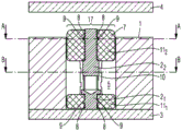
In the case of transmitting an asymmetric high-frequency signal, the high-frequency transmission path is designed as a coaxial transmission path. For this purpose, the coaxial transmission path preferably has a metallic outer conductor contact element 1 and a single metallic inner conductor 2, which inner conductor 2 is coaxial to the outer conductor contact element 1 and is arranged within the outer conductor contact element 1.
In a preferred embodiment, the outer conductor contact element 1 is realized by an electrically conductive intermediate part which is located between a first part 3, preferably a first high-frequency part, and a second part 4, preferably a second high-frequency part. The intermediate part corresponds to the housing and thus has an inner space 5, preferably in the shape of a cylinder, which inner space 5 extends between the first part 3 and the second part 4. The intermediate part serving as the outer conductor contact element 1 makes electrical contact with the corresponding outer conductor contact surfaces on the first part 3 and the second part 4.
The intermediate part serving as the outer conductor contact element 1 is rigidly shaped and thus has a fixed axial extension. Further, the intermediate part is mechanically fastened to the first part 3 and the second part 4. The mechanical connection may be, for example, a soldered connection and/or a screwed connection. As can be seen from fig. 1C, the first part 3 is connected by soldering to the intermediate part serving as the outer conductor contact element 1, while the second part 4 is fixed to the intermediate part by a screw connection. For this purpose, holes 14 aligned with one another are provided in the second part 4 and the intermediate part, respectively, and suitable screws 15 can be screwed into the holes 14, respectively. Preferably, the intermediate part is connected to the first part 3 and the second part 4 without leaving a slit opening.
The inner conductor 2 is located in an inner space 5 serving as an intermediate part of the outer conductor contact element 1 and is arranged coaxially with the outer conductor contact element 1 in this inner space 5. As shown in fig. 1C, in the assembled state, the inner conductor 2 extends between the respective inner conductor contact surfaces of the first and second parts 3, 4.
If there are a plurality of high-frequency transmission paths between the first part 3 and the second part 4, a plurality of mutually independent holes can be provided in the intermediate part, in each of which holes an inner conductor can be provided which is coaxial with the intermediate part serving as the outer conductor contact element 1. The intermediate member serves as a common outer conductor 1 for the individual coaxial high-frequency transmission paths.
Due to production process-induced errors in the flatness of the two mutually facing surfaces of the first part 3 and the second part 4 and in the flatness of the two end faces of the intermediate part serving as the outer conductor contact element 1, the distance between the two inner conductor contact surfaces of the first part 3 and the second part 4 will usually differ for different assemblies. Thus, there will be an axial deviation on the inner conductor side, which can be compensated by the inner conductor 2 having a variable axial extension.
To this end, the inner conductor contact according to the inventionThe axial extension of the element 17 is variable and comprises a solid first inner conductor part 21And a solid second inner conductor part 22Which are in electrical contact with each other on the one hand and are relatively movable in the axial longitudinal extension on the other hand.
First inner conductor part 21And a second inner conductor part 22Are all rigid parts, of which the first inner conductor part 21Only in the second inner conductor part 22The contact area has elasticity. Preferably, the first inner conductor part 21Is a component having a higher stiffness in the axial direction than in the radial direction, in particular at the area of contact with the second inner conductor part 22.
To realize the first inner conductor part 21And a second inner conductor part 22In reliable electrical contact with each other, the first inner conductor part 21Or the second inner conductor part 22At the inner conductor part 2 in contact with2Or 21Is formed as an elastic sleeve at the contact area. For example, in FIGS. 1A, 1B and 1C, the first inner conductor part 21Formed at its contact region as an elastic sleeve which contacts the second inner conductor part 2 at the distal end of its elastic butt strap 6 in a radially inwardly extending manner2Of the inner surface of (a).
The elastic sleeve of the first or second inner conductor part is designed to be in contact with the second inner conductor part 2 to be electrically contacted2Or the first inner conductor part 21Is movable longitudinally on the inner surface. Thus, in this way, the first inner conductor part 2 depends on the magnitude of the above-mentioned axial deviation1And a second inner conductor part 22Different lengths of overlap may be achieved. The effective axial extension of the inner conductor 2 is formed by the first inner conductor part 21And a second inner conductor part 22Is determined.
The first inner conductor part 2 of the spring-loaded inner conductor contact element 17 according to the invention1Electrically and mechanically fastens the respective contact surfaces of the first part 3. The mechanical fastening connection can be achieved here by means of the usual connection techniques, for example by welding. Optionally, a first inner conductor part21Only electrical contact with the first component 3 is possible. In this case, the second inner conductor part 2 is applied via the second component 42From the second inner conductor part 22To the first inner conductor part 21First inner conductor part 21And will thus be pressed against the relevant contact surface of the first component 3.
Likewise, as shown in fig. 1C, in the assembled state of the assembly according to the invention, the second inner conductor part 2 of the spring-loaded inner conductor contact element 17 according to the invention2In electrical contact with a corresponding contact surface of the second component 4. Optionally, the second inner conductor part 2 of the spring-loaded inner conductor contact element 17 according to the invention2Can be mechanically securely connected to the corresponding contact surface of the second part 4.
The first component 3 and the second component 4 are preferably high frequency components. Therefore, the first component 3 and the second component 4 may be generally a circuit board provided with a high-frequency electronic component, a case incorporating a high-frequency electronic component, a substrate incorporating a high-frequency electronic component, or a separate high-frequency component such as a high-frequency filter or a high-frequency amplifier.
In the spring-loaded inner conductor contact element 17 according to the invention, a spring element 7 of an electrically insulating material is arranged coaxially to the outer conductor contact element 1 and the inner conductor 2. Electrically insulating materials having elastic properties are preferably those suitable as elastomers, such as natural rubber, silicone, rubber or thermoplastic elastomers (TPE).
In the spring-loaded inner conductor contact element 17 according to the invention, the spring element 7 is fixed to the inner conductor 2, preferably with the spring element 7 both being fixed to the first inner conductor part 21Is fixed to the second inner conductor part 22The above. The claw 8 is preferably used as a fastening element, as is apparent in particular from fig. 1B, wherein fig. 1B is rotated by 90 ° about the longitudinal axis of the high-frequency transmission path in comparison with fig. 1A. These claws 8 are formed on the first inner conductor part 2, respectively1And a second inner conductor part 22And hooks into the recesses 9 at corresponding positions on the inner surface of the resilient element 7. The invention also includes other optional featuresBy means of, for example, gluing. Alternatively, in the spring-loaded inner conductor contact element 17 according to the invention, the spring element 7 can also be fixed only to the second inner conductor part 22The above.
By fixing the resilient element 7 to the inner conductor 2, preferably to the first inner conductor part 21And a second inner conductor part 22So that the first inner conductor part 21And a second inner conductor part 22Are resiliently connected together. By means of this elastic connection, the first inner conductor part 21And a second inner conductor part 22Are resiliently movable relative to each other. Thus, on the one hand, a variable axial extension of the inner conductor 2 can be achieved, which variable axial extension corresponds to when the first inner conductor part 2 is present1In contact with the first part 3 and the second inner conductor part 22The distance between the first part 3 and the second part 4 when in contact with the second part 4. On the other hand, the elastic connection is such that the first inner conductor part 21On the first part 3 and the second inner conductor part 22There is sufficient contact pressure on the second part 4.
In the case of a coaxial high-frequency transmission path, the spring element 7 of the spring-loaded inner conductor contact element 17 according to the invention is substantially sleeve-shaped. At a middle region 10 of the sleeve-shaped elastic element 7, the middle region 10 has two end regions 11 at the axial ends of the elastic element1And 112With a rigidity relative to the two end regions 111And 112The stiffness of the (c) is reduced.
For this purpose, two end regions 11 are provided1And 112Is reduced in comparison to the outer diameter of the elastic element 7 at the intermediate region 10. Furthermore, in the middle region 10 of the spring element 7, as can be seen from the three-dimensional view of the spring element 7 in fig. 1D, a plurality of slits 12 extending longitudinally in the axial direction of the spring element 7 of the spring-loaded inner conductor contact element 17 according to the invention are preferably arranged in an equidistant angular cross section. These slits 12 extend from the outer surface to the inner surface of the sleeve-like elastic element 7. The number of slits 12 can be appropriately selected.
Due to reduced outer diameterAnd a slit 12 arranged in the intermediate region 10, the diameter of the intermediate region 10 of the elastic element 7 being widened upon contraction of the elastic element 7, while the longitudinal extension of the intermediate region 10 of the elastic element 7 in the axial direction is shortened. The contraction of the elastic element 7 does not normally alter the end region 111And 112An axial longitudinal extension and an outer or inner diameter.
The rigidity of the intermediate region 10 of the elastic element 7 can be reduced by the additional provision of recesses 13 on the inner and/or outer surface of the intermediate region 10 of the elastic element 7.
The reduced outer diameter at the middle region 10 of the spring element 7, the gap 12 at the middle region 10 of the spring element 7 and the additional recess 13 are located opposite the two end regions 11 of the spring element 7 in the high-frequency transmission path1And 112The wave resistance at the portion where the intermediate region 10 of the elastic element 7 is located in the high-frequency transmission path is increased. In order to compensate for the change in wave resistance, the first inner conductor part 2 is arranged in the region of the spring-loaded inner conductor contact element 171And a second inner conductor part 22At the middle area 10 of the elastic element 7 than at the two end areas 12 of the elastic element 71And 122The area is large. In this way, the wave resistance of the high-frequency transmission path is effectively adjusted over the entire axial longitudinal extension.
As can be seen from fig. 1C, in the assembled state of the assembly, the axial longitudinal extension of the resilient element 7 at its ends is slightly reduced compared to the axial longitudinal extension of the inner conductor 2 and the outer conductor contact element 1. This slight reduction in the axial longitudinal extension makes it possible to provide the first inner conductor part 2 with a small axial longitudinal extension1And the outer conductor contact element 1 each being in more reliable electrical contact with the first part 3, and the second inner conductor part 22And the outer conductor contact element 1 each make more reliable electrical contact with the second component 4.
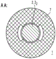
It should be noted here that the outer conductor contact is not realized by a single outer conductor contact element 1. In addition to a sleeve or plate with a hole as an integrally formed housing enclosing the spring-loaded inner conductor contact element 17 according to the invention between the first part 3 and the second part 4, the invention may also comprise an outer conductor contact structure consisting of a plurality of outer conductor contact elements. These outer conductor contact elements may for example be distributed on a concentric circle coaxial with the spring-loaded inner conductor contact element 17 or within a certain range around the spring-loaded inner conductor contact element 17.
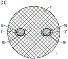
In a second variant, the spring-loaded inner conductor contact element 17' comprises a plurality of inner conductors. As shown in fig. 2A, 2B and 2C, in the spring-loaded inner conductor contact element 17', for example, there are two inner conductors 21And 22They transmit a differential high-frequency signal in common (so-called two-axis configuration). However, the invention is not limited to only two inner conductors. In addition, the present invention includes pairs of two inner conductors, each pair of conductors carrying a differential signal. When the inner conductors are arranged in a four-star shape, two pairs of two inner conductors may be arranged to cross each other, for example.
As shown in the sectional views of fig. 2B and 2C, in the case of the second deformation, the spring-loaded inner conductor contact element 17' comprises a plurality of inner conductors, so that the metallic inner conductor 21And 22The electrically insulating spring element 7' and the metallic outer conductor contact element 1 are not coaxial with each other.
As can be seen from fig. 2A, 2B and 2C, the spaced inner conductors 2 of the spring-loaded inner conductor contact element 17' are separated from one another1And 22And their solid first and second inner conductor parts 21 1、21 2Or 22 1And 22 2Is arranged inside the outer conductor contact element 1.
To realize two inner conductors 21And 22First and second inner conductor parts 21 1And 21 2Or 22 1And 22 2Relative elastic movability between the outer conductor contact element 1 and the two inner conductors 21And 22Between which an elastic element 7 'is arranged and which elastic element 7' is fixed to the two inner conductors 2, preferably by means of claws 81And 22. As shown in fig. 2A, for the elastic element 7' is fixedFixed to two inner conductors 21And 22Preferably both to the first inner conductor part 21 1And 22 1Is fixed to the second inner conductor part 21 2And 22 2The above. Is arranged on the inner conductor 21And 22Can hook into the corresponding recess 9 of the elastic element 7'.
In order to enable the spring element 7' to be produced as a cast part made of an electrically insulating material, preferably an elastomer, with the two inner conductor parts 21 1And 22 1The adjacent specific area 16 is not filled with the elastic element 7'.
Although the present invention has been fully described above based on the preferred embodiments, the present invention is not limited thereto but may be modified according to other various methods or manners.
Reference numerals:
1 outer conductor
11Outer conductor part
2,21,22Inner conductor
21,22First and second inner conductor parts
21 1,21 2,22 1,22 2First and second inner conductor parts of different inner conductor pairs
3 first part
4 second part
5 inner space of intermediate member serving as outer conductor
6 elastic butt strap
7, 7' elastic element
8 claw
9 concave part
10 middle region of elastic element
111,112End region of elastic element
12 gap
13 recess at the middle region of the elastic element
14 holes
15 screw
16 specific areas not filled by elastic elements
17, 17' spring-loaded inner conductor contact element
Claims (11)
1. A spring-loaded inner conductor contact element (7; 7') comprising:
at least one inner conductor (2; 2)1,22) And are and
surrounding the at least one inner conductor (2; 2)1,22) Of the elastic element (7; 7');
wherein the at least one inner conductor (2; 2)1,22) Is variable, the at least one inner conductor (2; 21,22) Is metallic, the elastic element (7; 7') made of electrically insulating material and fixed to each of said inner conductors (2; 21,22) The above.
2. Spring-loaded inner conductor contact element (7; 7 ') according to claim 1, characterized in that the electrically insulating material of the spring element (7; 7') is an elastomer.
3. Spring-loaded inner conductor contact element (7; 7 ') according to claim 1 or 2, characterized in that at both end regions (11) adjacent to the axial ends of the spring element (7; 7')/1,112) In between, the elastic element (7; 7') relative to the two end regions (11)1,112) The stiffness of the (c) is reduced.
4. Spring-loaded inner conductor contact element (7; 7') according to claim 3, characterized in that the contact endA region (11)1,112) Is reduced in comparison to the outer diameter at said intermediate region (10).
5. A spring-loaded inner conductor contact element (7; 7 ') according to claim 3 or 4, characterized in that the intermediate region (10) has a plurality of slits (12) extending longitudinally in the axial direction, the plurality of slits (12) extending from the outer surface of the spring element (7; 7') to the inner surface thereof.
6. Spring-loaded inner conductor contact element (7; 7 ') according to any one of claims 3 to 5, characterized in that the spring element (7; 7') is provided with at least one recess (13) in each case on the inner and/or outer surface at the middle region (10).
7. Spring-loaded inner conductor contact element (7; 7 ') according to any one of claims 3 to 6, characterized in that, in order to achieve a suitable wave resistance in the axial longitudinal extension of the spring-loaded inner conductor contact element (7; 7 '), the at least one inner conductor (2; 2 ') is made1,22) In the at least one inner conductor (2; 21,22) Adjacent to the elastic element (7; 7') is enlarged at the middle region (10).
8. Spring-loaded inner conductor contact element (7; 7') according to any one of claims 1 to 7, characterized in that the at least one inner conductor (2; 2)1,22) Comprising a solid first inner conductor part (2) connected to or in contact with a first component (3)1;21 1,22 1) And a second, solid inner conductor part (2) connected to or in contact with the second component (4)2;21 2,22 2);
Wherein the second inner conductor part (2)2;21 2,22 2) And said first inner conductor part (2)1;21 1,22 1) Electrically contacting and opposing the first inner conductor part (2)1;21 1,22 1) Moving;
the elastic element (7; 7') being fixed at least to the second inner conductor part (2)2;21 2,22 2) The above.
9. Spring-loaded inner conductor contact element (7; 7 ') according to any of claims 1 to 8, characterized in that the spring element (7; 7') is at each inner conductor (2; 2)1,22) Is fixed by means of a fixing provided on each inner conductor (2; 21,22) Is provided, said at least one jaw (8) being hooked onto said elastic element (7; 7') of the housing and corresponding recesses (9).
10. An assembly comprising a first part (3), a second part (4), a spring-loaded inner conductor contact element (7; 7') according to any one of the preceding claims, and at least one outer conductor contact element (1);
wherein the outer conductor contact element (1) is arranged adjacent to the spring-loaded inner conductor contact element (7; 7'); the first part (3) and the second part (4) are connected to each other by the at least one outer conductor contact element (1); and the number of the first and second electrodes,
at least one inner conductor (2; 7 ') of the spring-loaded inner conductor contact element (7; 7')1,22) Are connected to or in contact with the first part (3) and the second part (4), respectively.
11. A resilient element (7; 7 ') made of an electrically insulating material, wherein the resilient element (7; 7') is designed to be fixed to at least one inner conductor (2; 2 ') of a spring-loaded inner conductor contact element (7; 7') according to any one of claims 1 to 91,22) The above.
Applications Claiming Priority (3)
| Application Number | Priority Date | Filing Date | Title |
|---|---|---|---|
| DE102017009065.3 | 2017-09-28 | ||
| DE102017009065.3A DE102017009065A1 (en) | 2017-09-28 | 2017-09-28 | SPRING-LOADED INTERNAL CONTACT ELEMENT |
| PCT/EP2018/067282 WO2019063149A1 (en) | 2017-09-28 | 2018-06-27 | Spring-loaded inner-conductor contact element |
Publications (1)
| Publication Number | Publication Date |
|---|---|
| CN111164838A true CN111164838A (en) | 2020-05-15 |
Family
ID=62815022
Family Applications (1)
| Application Number | Title | Priority Date | Filing Date |
|---|---|---|---|
| CN201880063480.2A Pending CN111164838A (en) | 2017-09-28 | 2018-06-27 | Spring-loaded inner conductor contact element |
Country Status (6)
| Country | Link |
|---|---|
| US (1) | US11196204B2 (en) |
| EP (1) | EP3482465B1 (en) |
| CN (1) | CN111164838A (en) |
| DE (1) | DE102017009065A1 (en) |
| FI (1) | FI3482465T3 (en) |
| WO (1) | WO2019063149A1 (en) |
Cited By (1)
| Publication number | Priority date | Publication date | Assignee | Title |
|---|---|---|---|---|
| CN116917747A (en) * | 2021-12-23 | 2023-10-20 | 斯宾纳有限公司 | Broadband coaxial load |
Families Citing this family (2)
| Publication number | Priority date | Publication date | Assignee | Title |
|---|---|---|---|---|
| US11651986B2 (en) * | 2021-01-27 | 2023-05-16 | Applied Materials, Inc. | System for isolating electrodes at cryogenic temperatures |
| US11387587B1 (en) * | 2021-03-13 | 2022-07-12 | Plastronics Socket Partners, Ltd. | Self-retained slider contact pin |
Citations (6)
| Publication number | Priority date | Publication date | Assignee | Title |
|---|---|---|---|---|
| US5427535A (en) * | 1993-09-24 | 1995-06-27 | Aries Electronics, Inc. | Resilient electrically conductive terminal assemblies |
| US6079987A (en) * | 1997-12-26 | 2000-06-27 | Unitechno, Inc. | Connector for electronic parts |
| WO2001022537A1 (en) * | 1999-09-21 | 2001-03-29 | Rosenberger Hochfrequenztechnik Gmbh & Co. | Assembly of spring contacts in a predetermined raster |
| JP2004047268A (en) * | 2002-07-11 | 2004-02-12 | Shin Etsu Polymer Co Ltd | Insulation displacement connector |
| CN101228669A (en) * | 2005-07-20 | 2008-07-23 | 蒂科电子Amp有限责任公司 | Coaxial connector |
| CN205070039U (en) * | 2015-10-30 | 2016-03-02 | 罗森伯格(上海)通信技术有限公司 | Integrated multichannel inter -plate tolerance radio frequency connector |
Family Cites Families (12)
| Publication number | Priority date | Publication date | Assignee | Title |
|---|---|---|---|---|
| DE2421321C3 (en) * | 1974-05-02 | 1978-05-11 | Georg Dipl.-Ing. Dr.-Ing. 8152 Feldkirchen-Westerham Spinner | Sealed coaxial connector |
| US20040029433A1 (en) * | 2002-08-07 | 2004-02-12 | Andrew Corporation | Flexible coaxial adapter |
| DE20316337U1 (en) | 2003-10-22 | 2003-12-18 | Information Test Technology Co., Ltd., Shenkeng | Spring loaded contact element for electrical systems has contact pin and spring retained in a metal cylinder by an end plug element |
| DE202004005273U1 (en) * | 2004-04-02 | 2004-06-03 | Rosenberger Hochfrequenztechnik Gmbh & Co | Coaxial connector for printed circuit boards with spring-loaded tolerance compensation |
| JP2008145238A (en) * | 2006-12-08 | 2008-06-26 | Micronics Japan Co Ltd | Electrical connection apparatus and electric connection device using it |
| CN201029131Y (en) * | 2007-03-02 | 2008-02-27 | 富士康(昆山)电脑接插件有限公司 | Electric connector terminal |
| IT1395336B1 (en) | 2009-01-20 | 2012-09-14 | Rise Technology S R L | ELASTIC CONTACT DEVICE FOR ELECTRONIC COMPONENTS WITH COLLASSANT COLUMNS |
| DE202012000487U1 (en) * | 2012-01-19 | 2012-02-27 | Rosenberger Hochfrequenztechnik Gmbh & Co. Kg | connecting element |
| WO2013180692A1 (en) * | 2012-05-29 | 2013-12-05 | Intel Corporation | Substrate embedded electrical interconnect |
| US9490052B2 (en) | 2012-06-29 | 2016-11-08 | Corning Gilbert, Inc. | Tubular insulator for coaxial connector |
| DK2680372T3 (en) | 2012-06-29 | 2017-09-11 | Corning Optical Comm Rf Llc | Multiple section insulator for coaxial connector |
| KR102402669B1 (en) * | 2015-08-20 | 2022-05-26 | 삼성전자주식회사 | Connection structural member and connection structural member module, and probe card assembly and wafer testing apparatus using the same |
-
2017
- 2017-09-28 DE DE102017009065.3A patent/DE102017009065A1/en not_active Withdrawn
-
2018
- 2018-06-27 FI FIEP18736845.1T patent/FI3482465T3/en active
- 2018-06-27 WO PCT/EP2018/067282 patent/WO2019063149A1/en unknown
- 2018-06-27 US US16/650,422 patent/US11196204B2/en active Active
- 2018-06-27 EP EP18736845.1A patent/EP3482465B1/en active Active
- 2018-06-27 CN CN201880063480.2A patent/CN111164838A/en active Pending
Patent Citations (6)
| Publication number | Priority date | Publication date | Assignee | Title |
|---|---|---|---|---|
| US5427535A (en) * | 1993-09-24 | 1995-06-27 | Aries Electronics, Inc. | Resilient electrically conductive terminal assemblies |
| US6079987A (en) * | 1997-12-26 | 2000-06-27 | Unitechno, Inc. | Connector for electronic parts |
| WO2001022537A1 (en) * | 1999-09-21 | 2001-03-29 | Rosenberger Hochfrequenztechnik Gmbh & Co. | Assembly of spring contacts in a predetermined raster |
| JP2004047268A (en) * | 2002-07-11 | 2004-02-12 | Shin Etsu Polymer Co Ltd | Insulation displacement connector |
| CN101228669A (en) * | 2005-07-20 | 2008-07-23 | 蒂科电子Amp有限责任公司 | Coaxial connector |
| CN205070039U (en) * | 2015-10-30 | 2016-03-02 | 罗森伯格(上海)通信技术有限公司 | Integrated multichannel inter -plate tolerance radio frequency connector |
Cited By (1)
| Publication number | Priority date | Publication date | Assignee | Title |
|---|---|---|---|---|
| CN116917747A (en) * | 2021-12-23 | 2023-10-20 | 斯宾纳有限公司 | Broadband coaxial load |
Also Published As
| Publication number | Publication date |
|---|---|
| FI3482465T3 (en) | 2023-04-20 |
| EP3482465B1 (en) | 2023-02-22 |
| US11196204B2 (en) | 2021-12-07 |
| DE102017009065A1 (en) | 2019-03-28 |
| WO2019063149A1 (en) | 2019-04-04 |
| US20210167541A1 (en) | 2021-06-03 |
| EP3482465A1 (en) | 2019-05-15 |
Similar Documents
| Publication | Publication Date | Title |
|---|---|---|
| KR101936770B1 (en) | Contact device | |
| JP5905594B2 (en) | Connecting member | |
| JP5205453B2 (en) | Coaxial connector | |
| US20100159718A1 (en) | Coaxial Connector | |
| CN111164838A (en) | Spring-loaded inner conductor contact element | |
| CN103050793A (en) | Electrical coaxial connector | |
| EP3881397A1 (en) | Printed circuit board connector | |
| CN105359344A (en) | Plug-in connector | |
| JP7357962B2 (en) | Housing-integrated board mating connector and its manufacturing method | |
| CN110383585B (en) | Inner conductor element | |
| US20140073179A1 (en) | Coaxial connector suitable for connection of a flat plate-like connection object | |
| CN104662748A (en) | Insulating body of a plug-in connector | |
| JP2015517177A (en) | System for current transmission | |
| US9502825B2 (en) | Shunt for electrical connector | |
| JP4812113B2 (en) | Board connector | |
| JP6610309B2 (en) | Coaxial connector device | |
| WO2009113474A1 (en) | Antenna device | |
| CN110752461B (en) | Connector between parallel plates | |
| CN103887626A (en) | Coaxial connector | |
| CN104051910B (en) | Current divider for electric connector | |
| KR101532399B1 (en) | Conector for printed circuit board | |
| CN116830392A (en) | Electrical plug-in connector and printed circuit board device | |
| CN114696142A (en) | Connector and connector assembly | |
| CN111224265A (en) | Connector with a locking member | |
| JPH07183069A (en) | Coaxial connector structure |
Legal Events
| Date | Code | Title | Description |
|---|---|---|---|
| PB01 | Publication | ||
| PB01 | Publication | ||
| CB03 | Change of inventor or designer information |
Inventor after: Benedict Schwarz Inventor after: Andreas Gruber Inventor after: Johannes hobeck Inventor before: Benedict Schwarz Inventor before: Johannes Gruber Inventor before: Johannes hobeck |
|
| CB03 | Change of inventor or designer information | ||
| SE01 | Entry into force of request for substantive examination | ||
| SE01 | Entry into force of request for substantive examination |