CN1111299C - Non-contact IC card and non-contact IC card system - Google Patents
Non-contact IC card and non-contact IC card system Download PDFInfo
- Publication number
- CN1111299C CN1111299C CN95117764A CN95117764A CN1111299C CN 1111299 C CN1111299 C CN 1111299C CN 95117764 A CN95117764 A CN 95117764A CN 95117764 A CN95117764 A CN 95117764A CN 1111299 C CN1111299 C CN 1111299C
- Authority
- CN
- China
- Prior art keywords
- circuit
- card
- phase
- antenna resonance
- resonance circuit
- Prior art date
- Legal status (The legal status is an assumption and is not a legal conclusion. Google has not performed a legal analysis and makes no representation as to the accuracy of the status listed.)
- Expired - Fee Related
Links
Images


Classifications
-
- G—PHYSICS
- G06—COMPUTING; CALCULATING OR COUNTING
- G06K—GRAPHICAL DATA READING; PRESENTATION OF DATA; RECORD CARRIERS; HANDLING RECORD CARRIERS
- G06K19/00—Record carriers for use with machines and with at least a part designed to carry digital markings
- G06K19/06—Record carriers for use with machines and with at least a part designed to carry digital markings characterised by the kind of the digital marking, e.g. shape, nature, code
- G06K19/067—Record carriers with conductive marks, printed circuits or semiconductor circuit elements, e.g. credit or identity cards also with resonating or responding marks without active components
- G06K19/07—Record carriers with conductive marks, printed circuits or semiconductor circuit elements, e.g. credit or identity cards also with resonating or responding marks without active components with integrated circuit chips
-
- G—PHYSICS
- G06—COMPUTING; CALCULATING OR COUNTING
- G06K—GRAPHICAL DATA READING; PRESENTATION OF DATA; RECORD CARRIERS; HANDLING RECORD CARRIERS
- G06K7/00—Methods or arrangements for sensing record carriers, e.g. for reading patterns
- G06K7/0008—General problems related to the reading of electronic memory record carriers, independent of its reading method, e.g. power transfer
-
- G—PHYSICS
- G06—COMPUTING; CALCULATING OR COUNTING
- G06K—GRAPHICAL DATA READING; PRESENTATION OF DATA; RECORD CARRIERS; HANDLING RECORD CARRIERS
- G06K19/00—Record carriers for use with machines and with at least a part designed to carry digital markings
- G06K19/06—Record carriers for use with machines and with at least a part designed to carry digital markings characterised by the kind of the digital marking, e.g. shape, nature, code
- G06K19/067—Record carriers with conductive marks, printed circuits or semiconductor circuit elements, e.g. credit or identity cards also with resonating or responding marks without active components
- G06K19/07—Record carriers with conductive marks, printed circuits or semiconductor circuit elements, e.g. credit or identity cards also with resonating or responding marks without active components with integrated circuit chips
- G06K19/0723—Record carriers with conductive marks, printed circuits or semiconductor circuit elements, e.g. credit or identity cards also with resonating or responding marks without active components with integrated circuit chips the record carrier comprising an arrangement for non-contact communication, e.g. wireless communication circuits on transponder cards, non-contact smart cards or RFIDs
Landscapes
- Engineering & Computer Science (AREA)
- Physics & Mathematics (AREA)
- General Physics & Mathematics (AREA)
- Theoretical Computer Science (AREA)
- Computer Hardware Design (AREA)
- Microelectronics & Electronic Packaging (AREA)
- Artificial Intelligence (AREA)
- Computer Vision & Pattern Recognition (AREA)
- Computer Networks & Wireless Communication (AREA)
- Near-Field Transmission Systems (AREA)
- Credit Cards Or The Like (AREA)
Abstract
A non-contact type IC card system comprising a non-contact type IC card using an electromagnetic wave as a communication medium and not containing a battery therein, and a reading and writing (R/W) unit. To eliminate a problem that the level of a received signal varies depending upon the communication distance between the card and the R/W unit, a comparator 7 detects the received signal level of an antenna resonance circuit 4 for data transmission and reception, before a variable resistance device 8 alters the quality factor Q of the antenna resonance circuit 4, which results in adjusting the level of the received signal being inputted to a desirable value.
Description
The present invention relates to use the non-contact IC card and the contactless IC card system that use this non-contact IC card of electromagnetic wave as communication medium.
Figure 43 illustrates the general formation of the known contactless IC card system that includes non-contact IC card, wherein uses electromagnetic wave as communication medium.In the diagram, this IC-card system comprises non-contact IC card (below be referred to as card) 1, read/write device (brief note is R/W) 2, and the principal computer 3 that is connected with R/W device 2.That is to say that non-contact IC card is used system and generally included card 1, can carry out the R/W unit 2 of read data operation from card, and in order to the principal computer 3 of control total system, both can constitute a unit (R/W unit) R/W unit 2 and principal computer 3.The application electromagnetic wave that transmits and receive data between card 1 and R/W2 carries out as medium.
But, the contactless IC card system of this such formation that has earlier can not produce satisfied result for satisfied following requirement: (1) from reducing manufacturing cost, and the problem of exempting the influence of battery life and being beneficial to environmental protection needs a kind of no battery card that need not internal battery; (2) depend on the place of application, the signal level that is received is wanted and can be changed according to the distance of communication, i.e. distance between card and the R/W unit, and requiring by this distance is adjustable at a side's who blocks incoming level; (3) except effective power transmission and receiving, in order to realize to reduce power consumption (demand) as far as possible with the telecommunication of not having the battery card; (4) for from the R/W unit to the card communication, the transmission of data will be carried out simultaneously with power supply, at this moment because continuous power supply is impossible in the mode of amplitude modulation, thus must phase modulation or frequency modulation, and at this moment when the side reception of card, must carry out demodulation with the less current loss; And (5) are when R/W unit one side receives the data that sent, side's power to card sends and can once stop, owing to this reason, card must can only lean against the energy efficient that accumulates in the power supply and operate sending necessary data volume, thereby must modulate effectively.
In order to satisfy above requirement, carry out development of the present invention, and particularly the purpose of this invention is to provide a kind of non-contact IC card and contactless IC card system, the both can be according to the sensitivity of the level switched antenna of the signal that receives.
For this purpose, according to an aspect of the present invention, provide and used electromagnetic wave does not also wherein contain battery as communication medium non-contact IC card, it comprises the incoming level detecting device that is connected with the antenna resonance circuit that is used for data transmission and reception, in order to detect the signal level that is received, also comprise the quality factor regulator that also is connected, be used for as the quality factor q that changes or change antenna resonance circuit with the effect of the level that the incoming level detecting device detected with antenna resonance circuit.Signal level that so this structure is based in the antenna resonance circuit to be received and change the quality factor q of antenna resonance circuit.So this structure can provide a kind of non-contact IC card, wherein induced voltage can generate on the very wide scope of the variable in distance of read and write unit reposefully.
Another aspect of the present invention is, a kind of electromagnetic wave of using is as communication medium and wherein do not contain the non-contact IC card of battery, comprise: be used to detect phase detectors in order to the free-running phase place of carrying out the antenna resonance circuit that data send and receive, with the energy feeder, be used for when sending providing energy to antenna resonance circuit from energy storage circuit by the free-running phase place of antenna resonance circuit.That is, when sending with the free-running phase place of detected antenna resonance circuit from energy storage circuit to the antenna resonance circuit makeup energy.This structure can keep free oscillation effectively and guarantee long transmission.
Another aspect of the present invention is, uses electromagnetic wave and comprises as communication medium and a kind of non-contact IC card of wherein not containing battery: phase detectors are used to detect the free-running phase place of carrying out the antenna resonance circuit that data send and receive; With the resonance frequency switch, be used for inserting on antenna resonance circuit or disconnecting capacitor to change the resonance frequency of antenna resonance circuit from it according to one of the variation of output data and output data and output of phase detectors, wherein data send and are based on that one of frequency modulation or phase modulation carry out.So, capacitor carries out as the function of the variation of output data or output data to the access of antenna resonance circuit or from its disconnection, make that the network constant of antenna resonance circuit is that resonance frequency changes, and the transmission of data realizes by frequency modulation or phase modulation.This structure can be modulated effectively with less energy transmission loss.
Characteristics of the present invention are, use electromagnetic wave and comprise transmission and the reception that an antenna resonance circuit that is made of a series of resonant circuits is used for data as communication medium and the non-contact IC card that wherein do not contain battery.Because antenna resonance circuit is made of a series of resonant circuits with low resonance impedance, receive so can carry out effective power.
Another characteristics of the present invention are, use electromagnetic wave as communication medium and do not contain a non-contact IC card composed as follows of battery in it: the phase change detecting device is used for detecting based on its oscillation amplitude change and is used for the variation because of the caused voltage-phase of signal that received of antenna resonance circuit that data send and receive; And detuner, be used for according to the detected phase change of phase change detecting device the data demodulation.These characteristics according to the present invention, modulation phase modulation (PM) to data, at this moment detected phase change based on its oscillation amplitude change, made the modulation of finishing data according to detected phase change owing to the caused antenna resonance circuit of receiving of signal.So, can be undertaken by phase modulation to the transmission of card from read-write cell, this makes power supply and data transmission to be compared, and in addition, can save operating energy, therefore the demodulation in side's phase change of blocking realizes according to oscillation amplitude change.
Another characteristics of the present invention are, using electromagnetic wave to comprise as communication medium and the non-contact IC card that wherein do not comprise battery is used for according to the switching device of output data with the two-terminal short circuit of antenna resonance circuit, this antenna resonance circuit is transmission that is used for data and the reception that is made of the serial resonant circuit, thus, sending the variation be based on owing to the antenna resonance circuit load of switching device carries out.That is, the short circuit between the antenna resonance circuit two ends produces according to output data, sets up and send the load variations that is based on the antenna resonance circuit that is caused.The modulation of the less loss of energy when non-contact IC card that this structure provides can send effectively.
In addition, according to an aspect of the present invention, provide with electromagnetic wave as communication medium and wherein do not comprise the non-contact IC card and the read-write cell of battery, this non-contact IC card comprises the switching device that short circuit is carried out at the two ends of the antenna resonance circuit that is configured for data by the serial resonant circuit and sends and receive according to output data, makes that sending the variation that is based on owing to the load of the antenna resonance circuit of switching device carries out.Read while write the unit and comprise detuner, be used for carrying out demodulation by detecting based on the variation of regulating the card aspect of the variation that resistance took place with the power delivery of antenna resonant circuit connection.Aspect card, the two ends of antenna resonance circuit according to output data by short circuit, feasible transmission is based on the variation of antenna resonance circuit load and finishes, simultaneously aspect read-write cell, demodulation be by send based on the power that connects with the antenna resonant circuit regulate the change-detection that taken place in the resistance to the variation of card aspect load carry out.This structure can provide the contactless IC card system that can modulate effectively with less energy loss.
And then, comprise with electromagnetic wave as communication medium and do not comprise the non-contact IC card of battery in it and the contactless IC card system of a read-write cell in, read-write cell comprises the mandatory phase place phase inverter that is connected between the two ends that are used to the antenna resonance circuit that sends and receive, this phase inverter be used for respect to the variation of data ± 90 ° of scopes are to the short circuit at antenna resonance circuit two ends, to force to be sent out the paraphase of signal phase.In this structure, mandatory phase inverter to the antenna resonance circuit two ends with respect to data variation ± carry out short circuit in 90 ° of scopes, paraphase with the signal phase forcing to carry out to be sent, consequently, also can aspect read-write cell, carry out high speed data modulations even the Q value of antenna resonance circuit is very high.And, improved data transmission speed from read-write cell to card.
Preferably also comprise mandatory phase place paraphase speed regulator, the quick variation of voltage in the antenna resonance circuit in the time of can being suppressed at mandatory phase place paraphase effectively.Mandatory phase place paraphase speed regulator of this extra installing has been controlled the quick variation of antenna resonance circuit voltage when mandatory phase place paraphase, so also can normally send the Q value reduction of antenna resonance circuit even card closely makes from read-write cell.This structure can provide the contactless IC card system of high reliability, even when this system has reduced the Q value of the antenna resonance circuit aspect the card at the nearly read-write cell of clamping, also can normally set up communication.
And, according to an aspect of the present invention, be that communication medium and the non-contact IC that does not contain battery are installed with phase regulator with the electromagnetic wave, be used for causing and the synchronous induced voltage of the vibration of resonant circuit at antenna resonance circuit because of the signal that receives.This phase regulator causes that forcibly the phase place of the voltage of responding to because of the signal that receives in the antenna resonance circuit overlaps with the oscillation phase of this resonant circuit, although thereby make the high also practicable rapid data demodulation of Q value of antenna resonance circuit aspect card, so improved data transmission speed from read-write cell to the card aspect.
Be preferably in again and also comprise phase change detection rejector in the non-contact IC card, the effect of this rejector is the detection that suppresses phase change for phase detectors after intact in one given period, so that prevent because of ignoring little amplitude once more by demodulation prior to the phase-adjusted phase change unnecessary data when detected phase changes.Proper communication under the situation that Q value antenna resonance circuit is low even this phase change detection rejector can guarantee card and read-write cell is very near each other.That is,, this structure can normally set up the contactless IC card system of communication even can making the Q value of the antenna resonance circuit aspect the card reduce also can provide highly reliably at the nearly read-write cell of clamping.
Further characteristics of the present invention are, are that communication medium and the non-contact IC that does not contain battery are installed with the electromagnetic wave: rectification circuit is used for the signal of the antenna resonance circuit that sends from data and receive is carried out rectification; And switching device, this device can be operated according to switching signal, makes a ground connection that presents low voltage in two terminations of antenna resonance circuit, and wherein the high voltage of another termination is selected as a signal.This structure makes the amplitude of antenna resonance circuit become big, makes it be easy to processing signals in addition, because the signal of all gained all is positive.
Above-mentioned switching device preferably is equipped with a signal generating circuit, and this circuit produces switching signal, and it is exported when the high voltage signal transition of antenna resonance circuit is negative level by paraphase.That is, the high voltage signal of paraphase output is automatically converted to negative level, makes low voltage be grounded and allows high voltage to get as signal.
Also comprise in above-mentioned non-contact IC card again: PLL can receive or import the received signal of expression and be converted into the signal of negative state and produce one and be adjusted to the output of coordinating with input signal; And a detecting device, but the every half period of response phase modulation signal is for taking a sample based on the switching signal of PLL output and being used for modulation.Promptly, the operation of PLL is in order to receive the signal of the negative received signal of expression, and produce one with the output of its coordination, simultaneously, demodulation is to finish with switching signal based on the reception of sampled phase modulated signal of per semiperiod of the output of PLL the time, and consequently detecting the change in voltage that becomes for the card that is received has resistant function.
In above-mentioned non-contact IC card, when counting, the zero crossing of the waveform of given antenna resonance circuit just carries out the paraphase of above-mentioned switching signal, make to produce the transmission frequency that is different from power-frequency, make transmission carry out in can becoming at the shape of received power.And, when a zero cross point, just the carrying out of the waveform of the paraphase of above-mentioned switching signal in antenna resonance circuit, and when modulation, just carry out the paraphase of above-mentioned switching signal during four zero cross points of the waveform in antenna resonance circuit.So frequency is that the carrier wave of power-frequency 1/2 can receive generation simultaneously with power, and then by phase modulation.And in when modulation, the waveform in the antenna resonance circuit is just carried out the paraphase of above-mentioned switching signal by each zero cross point of four zero cross points, and this makes phase modulation to carry out based on four kinds of phase places.
With this structure, because increased the quantity of information of the every data in the transmission, the transmission of data can be carried out at a relatively high speed.
Another characteristics of the present invention are, above-mentioned non-contact IC card comprises PLL, its operation can receive the expression received signal and be converted to the signal of negative state and produce the consistent output of signal with input, wherein two upper ends that obtain semiperiod and above-mentioned antenna resonance circuit from the output of PLL for phase modulation when modulating from semiperiod that zero crossing is lighted by short circuit.This structure need not can realize the high speed demodulation by capacitor.Similarly, for phase demodulating, from the output of PLL obtain the semiperiod and when the modulation from two terminals of the above-mentioned antenna resonance circuit of zero cross point by the short circuit half period.This structure also can realize need not the high speed demodulation of capacitor.
And, according to an aspect of the present invention, above-mentioned capacitor is connected with antenna resonance circuit in one-period, and in two cycles with its disconnection, and be produced as the transmission frequency of 1/2 (half) power-frequency so that send simultaneously at state with received power.In contrast, when modulation, phase modulation is performed such, and promptly capacitor disconnected in one-period.This structure can produce the transmission carrier wave at the state of received power simultaneously and carry out transmission based on phase modulation.
Purpose of the present invention and characteristics will become more apparent from the detailed description below in conjunction with the preferred embodiment that accompanying drawing carried out.These accompanying drawings are:
Fig. 1 is a circuit diagram, and expression is according to the structure of the contactless IC card system of first to the 3rd embodiment of the present invention;
Fig. 2 is an oscillogram, is used for the operation of key diagram 1 circuit structure;
Fig. 3 is a circuit diagram, another structure of expression non-contact IC card;
Fig. 4 is a circuit diagram, another structure of expression contactless IC card system of the 4th to the 6th embodiment according to the present invention;
Fig. 5 is an oscillogram, is used for the operation of key diagram 4 circuit structures;
Fig. 6 is a circuit diagram, another structure of expression non-contact IC card;
Fig. 7 is for the resulting illustrative diagram of the delay of the data transmission in the seventh embodiment of the invention;
Fig. 8 is the diagram according to the circuit structure of the read-write cell of contactless IC card system of the present invention;
Fig. 9 is an oscillogram, is used for the operation of the read-write cell of presentation graphs 8;
Figure 10 is an oscillogram, is used for the phase modulation of presentation graphs 8 read-write cells;
Figure 11 A and 11B are oscillograms, are used for representing the accepting state at the low situation downward modulation phase time card of the Q of resonant circuit value according to the 7th embodiment;
Figure 12 A and 12B are oscillograms, are used for representing the transmit status according to the read-write cell of the eighth embodiment of the present invention;
Figure 13 is an oscillogram, is used for representing the receive status of ninth embodiment of the invention under the high situation of the Q of resonant circuit value;
Figure 14 is an oscillogram, is used for illustrating the demodulation according to the card of the 9th embodiment;
Figure 15 is an oscillogram, is used for describing the demodulation of the 9th embodiment when the Q of resonant circuit value is low;
Figure 16 is the circuit structure diagram according to non-contact IC card of the present invention;
Figure 17 is the diagram according to an example of the circuit structure of the non-contact IC card of the 11st embodiment of the present invention;
Figure 18 A and 18B represent the waveform in the circuit structure of card of Figure 17;
Figure 19 represents to produce according to the switching signal of the 12nd embodiment of the present invention structure of circuit;
Figure 20 represents the waveform of Figure 19 circuit structure;
Figure 21 is the diagram according to an example of the circuit structure of the test section of the non-contact IC card of thriteenth embodiment of the invention;
Figure 22 represents the waveform of Figure 21 test section circuit structure;
Figure 23 is an oscillogram, and expression is according to the operation of the non-contact IC card of the 14th embodiment of the present invention;
Figure 24 is an oscillogram, the complex wave that expression forms owing to the combination of 1/2 frequency of standard frequency and standard frequency;
Figure 25 is an oscillogram, is used to illustrate the operation according to the non-contact IC card of fifteenth embodiment of the invention;
Figure 26 A and 26B are oscillograms, represent the actual signal among the 15 embodiment;
Figure 27 A and 27B are oscillograms, are used to illustrate the operation according to the non-contact IC card of sixteenth embodiment of the invention;
Figure 28 represents an example of card circuit structure, and wherein data send and carry out with the bi-phase shift keying pattern, and it is 1/2 power-frequency that this pattern has been used carrier frequency;
Figure 29 represents the structure of another card circuit, and wherein data transmission is to be that the binary phase shift keying pattern of 1/2 power-frequency is carried out to have used carrier frequency;
Figure 30 represents an example of card circuit structure, carries out with the quadriphase PSK pattern by this routine data transmission, and having used frequency is the carrier wave of power-frequency 1/2;
Figure 31 is the diagram with an example of the circuit structure of the card of the data transmission of bi-phase shift keying pattern, and having used its frequency is the carrier wave of 1/4 power-frequency;
Figure 32 is the diagram of an example of carrying out the card circuit structure of data transmission with the quadriphase PSK pattern, and having used frequency is the carrier wave of 1/4 power-frequency;
Figure 33 A and 33B are oscillograms, and expression Figure 28 is to the operation of 32 circuit;
Figure 34 is the diagram according to an example of the circuit structure of the non-contact IC card of the 17th embodiment of the present invention;
Figure 35 is the waveform diagram in Figure 34 circuit;
Figure 36 A and 36B are the diagrams according to circuit structure one example of the non-contact IC card of the 18th embodiment of the present invention;
Figure 37 is the waveform diagram in Figure 36 circuit;
Figure 38 is the diagram according to an example of the circuit structure of the non-contact IC card of nineteenth embodiment of the invention;
Figure 39 is the diagram of the waveform in Figure 38 circuit;
Figure 40 A is the diagram of blocking a side and read-write cell one side's waveform among the 19 embodiment to Figure 40 C, and this obtains by simulation analysis of computer;
Figure 41 is the oscillogram that is used to describe according to the operation of the non-contact IC card of the 20th embodiment of the present invention;
Figure 42 A is the diagram of blocking the waveform among a side and read-write cell one side among the 20 embodiment to Figure 42 C, and this is obtained by simulation analysis of computer;
Figure 43 is the diagram of the known structure of non-contact IC card system.
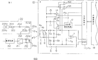
Now referring to Fig. 1, below explanation is according to first embodiment of the present invention contactless IC card system.In diagram, contactless IC card system represents with label 100 all, and it comprises no battery non-contact IC card (following will be referred to as card) 10 and read-write cell (below be designated as R/W) 20 substantially.Card 10 comprises the antenna resonance circuit 4 of the antiresonant circuit that is made of aerial coil 4a and capacitor 4b, also comprises by rectifying device 5a, and the rectification circuit 5 that 5b constitutes, and by store energy capacitor 6a, the energy storage circuit 6 that 6b forms.Attach, Fig. 1 expresses the structure of full-wave voltage doubler.Also comprise that at card the comparer 7 that is connected with reference power supply 7a is used to detect the situation of the voltage of rectification above predetermined value in 10, also comprise by the variable resistor device 8 that element constituted such as the mosfet transistor in parallel with antenna resonance circuit 4.When comparer 7 detected commutating voltage and surpasses predetermined value, variohm 8 changed the quality factor q of (or it is changed) antenna resonance circuit 4 according to exceeding (with it poor) amount of predetermined value.Wherein also comprise output transistor 9, output capacitor 11, transistor driver circuit 12, driver 14, its responsive control signal and enter executing state when sending, and the resistor 15 that is connected with the outgoing side of this driver 14.
In addition, card 10 also is equipped with: hot side level comparator 16a, and the amplitude level in the hot side of its function detection antenna resonance circuit 4 exceeds predetermined value (for example, Vcc); Low potential side level comparator 16b, the amplitude level height that is used for detecting the low level side of antenna resonance circuit 4 must be lower than predetermined value (for example, GND); In level comparator 16c, be used to detect antenna resonance circuit 4 and be higher than or be lower than predetermined value (for example, 1/2 Vcc); And control section 177 also is housed and is used to store memory of data part 18.Point out that in passing memory portion 18 can be made of similar devices that does not need to back up such as EEPROM, and is no battery types because block 10.
On the other hand, R/W unit 20 is equipped with: the antenna resonance circuit 201 that is used to send, and it constitutes series resonant circuit by aerial coil 201a and capacitor 201b and forms; Power sends regulating resistor 202, is used to regulate 20 watt levels that send from the R/W unit; Driver 203; And the modulation circuit of forming by an EX-OR circuit and be connected 204 with the input side of driver 203.204 couples of data 204a of modulation circuit and carrier wave 204b response.In addition, R/W unit 20 also is equipped with: the antenna resonance circuit 204 that is used to receive, and it is formed antiresonant circuit by aerial coil 210a and capacitor 210b and constitutes; Be used to amplify the amplifying circuit 211 of the signal that is received; And demodulator circuit 212.
Owing to can change a lot with the supply between R/W unit 20 and the card 10 apart from power, so being based on the voltage that rectification goes out in the change of card 10 1 side's quality factor qs carries out, so that be stabilized in the voltage that is induced in the card 10, form absorption like this to the variation of power supply.In the formation of Fig. 1, comparer 7 forms the incoming level detecting device with reference power supply 7a, and variable resistor device 8 constitutes the quality factor regulator.
In operation, the voltage after comparer 7 detects rectification surpasses under the situation of predetermined value.Variohm 8 is conditioned and makes the quality factor q of antenna resonance circuit 4 become lower, and this is as a function that departs from predetermined value.The reducing of quality factor q makes that the voltage that is received is adjustable, and therefore, the variation that the voltage that is induced in the card 10 can overcome because of the distance between R/W unit 20 and the card 10 can keep stablizing.
Embodiment 2
Now the second embodiment of the present invention is described again in conjunction with Fig. 2.The aspect of second embodiment is as follows.Promptly, data are to carry out under such state from the transmission that blocks 10 to R/W unit 20, promptly need the transmission of big transmitted power to stop, but the supply of electric energy in this case simultaneously also stopped from R/W unit 20 to card 10, thereby the energy of store in card 10 effectively.For this reason, in the present embodiment, be to occur in free oscillation in the antenna resonance circuit 4 by direct utilization to cause the energy that is stored among energy-storage capacitor 6a and the 6b be the antenna resonance circuit 4 that little by little offers card 10, consequently the time of free-running decay carries out longly.
In the present embodiment, intermediate level comparer 16C has constituted phase detectors, and driver 14 has constituted energy with resistor 15 device is provided.Driver 14 is made of a circuit, Nch strings of transistors of one of them Pch transistor AND gate is connected between power supply and the reference level, be the two ends of energy storage circuit 6, and be used for providing by resistor 15 energy of energy storage circuit 6 to antenna resonance circuit 4.
In operation, driver 14 responsive control signal 14a when sending transfers execution state to.Detect the phase place of antenna resonance circuit 4 based on the output of intermediate level comparer 16, provide energy-storage capacitor 6a to antenna resonance circuit 4, the energy among the 6b according to necessary amount of the free oscillation of keeping antenna resonance circuit 4 and wherein free oscillation same-phase ground.At this moment, the adjusting of quantity delivered depends on the resistance of resistor 15, can prolong from the transmitting time of blocking 10 thus.
Embodiment 3
Below still constitute the explanation third embodiment of the present invention with reference to the circuit of Fig. 1.For also must less energy consumption from blocking the modulation that 10 to R/W data send.Thereby in the present embodiment, the constant of antenna resonance circuit 4 changes according to the variation of the data of being transmitted, and has realized pm mode with this.
In the present embodiment, intermediate level comparer 16C has formed phase detectors, and output transistor 9, output capacitor 11 has constituted the resonance frequency switching device with transistor driver circuit 12.The type of transistor driver circuit 12 makes provides a signal to output transistor 9 when the pulsed output data of control section 17 changes.
The operation of present embodiment is as follows.Under the situation of phase modulation, when output data changed, transistor driver circuit 12 produced 180 ° the pulse that one 180 ° of phase cyclings rise.The output that these 180 ° of phase cyclings are based on intermediate level comparer 16c obtains.Thereafter, output transistor 9 makes the resonance frequency of antenna resonance circuit 4 change according to the variation of data according to these 180 ° of pulses and turn-on and turn-off have consequently taken place by switching on and off of 11 pairs of antenna resonance circuits 4 of output capacitor.Output capacitor 11 and the result who is connected of antenna resonance circuit 4 cause the variation of the network constant of antenna resonance circuit 4.
Fig. 2 is used for representing the oscillogram of operating, (a) representative data wherein, (b) expression carrier wave, (c) represent the waveform of phase modulation, (d) be illustrated in the signal (180 ° of pulses) that offers transistor 9 base stages in the phase modulation, (e) waveform of expression behind the frequency modulation, and (f) present signal during expression frequency modulation to the base stage of transistor 9.From Fig. 2 (a) to (d) obviously as seen, when output data changes (otherwise from the H level to the L level or), then frequency change reaches 180 ° cycle.At this moment, set the frequency changed and be 1/2 of original frequency, can realize the 2-phase modulation (PM).Promptly as shown in Fig. 2 (c), the signal of phase modulation presents in frequency to 1/2 variation and reaches 180 ° of cycles, promptly for alphabetical A to the cycle between the B, the paraphase of phase place took place by the variation of this frequency cycle between letter C and D.On the other hand, if phase place is considered in the output based on intermediate level phase comparator 16c, then output transistor 9 is directly according to the variation of the output data of slave controller part 17 and turn-on and turn-off, at this moment as (e) of Fig. 2 and (f) shown in can realize making frequency to be reduced to 1/2 frequency modulation.
These modulating systems need less energy for the frequency modulation of card 10.Need not carry out modulation by the driven antenna resonant circuit for this reason.
Though the section construction that comprises rectification circuit 5 and tank circuit 6 in the formation of Fig. 1 is full-wave voltage doubler as shown in Figure 3, but also can be configured to comprise the half-wave voltage-doubler rectifier of rectification circuit 5, this rectification circuit 5 is by rectifying device 5a, and 5b and the tank circuit 6 that is formed by a capacitor constitute.And, also be practicable such as rectifier systems such as half-wave rectification and bridge rectifiers.
Fig. 4 is the diagram according to another formation of contactless IC card system of the present invention.In this diagram, what the card system was total represents with label 110, comprises card 10b and R/W unit 20b similarly.In the system of Fig. 4, be marked with identical label corresponding to the parts of Fig. 1, and it is illustrated as is omitted for the purpose of simple and direct.And, be omitted for the only relevant part of the 3rd embodiment among Fig. 4 with front first embodiment.The characteristics of R/W unit 20a are all antenna resonance circuit 201A will be arranged for sending and receiving.
Below describe with regard to the fourth embodiment of the present invention referring to Fig. 4.10b presents under the situation of big current drain at card, and sending to effective electric energy of card 10b from the R/W unit need low-impedance antenna resonance circuit 4A.Thereby in the 4th embodiment, the antenna resonance circuit 4A of card 10b is configured to series resonant circuit, and wherein aerial coil 4a and capacitor 4b are coupled with being one another in series, makes power absorb by the antenna resonance circuit 4A that is made of low-impedance series resonant circuit.This formation can be carried out electric energy effectively and be received in card 10b.
Still in conjunction with Fig. 4 the fifth embodiment of the present invention is described.Promptly send data when 10g provides electric energy from R/W unit 20a to card, to provide to be impossible to continuous electric energy when amplitude modulation.Thereby phase modulation or frequency modulation then are necessary.So, according to this 5th embodiment, for from R/W unit 20a to the card energy supply of 10b and data send and can carry out compatible with each otherly, to carry out phase modulation to data, and be the variation of amplitude and detected with the variation of the phase place of the signal that antenna resonance circuit 4A the was received demodulation by data as change in voltage the side of card 10b.
In the present embodiment, the level comparator 16a of high-side and the level comparator 16b of low level side constitute the phase change detecting device, intermediate level comparer 16c, and control section 17 grades constitute detuner.
Fig. 5 is an oscillogram, is used for illustrating that data stand under the situation of phase modulation the card signal that 10b received to be carried out the operation of demodulation.Among Fig. 5, (a) waveform among the expression antenna resonance circuit 4A, (b) output waveform of expression hot side level comparator 16a, (c) output waveform of expression low potential side level comparator 16b, and the output waveform of (d) representing intermediate level comparer 16c.
The demodulation of the signal that card is received among the 10b is to reach by the variation that detects the signal amplitude that is received when the phase change of the signal that receives.Device 16a based on the comparison, the output of 16b judges: when the signal (amplitude) that receives surpasses the voltage of rectification phase change has not taken place, and carried out the demodulation of data according to this judgement.From the variation of amplitude and the variation of detected phase can reduce side's operating current of card 10b.So, except data transmission and power supply energy are compatible with each other, blocking the operational power that 10b one can reduce to separate timing.Though above explanation is carried out card 10b, card 10 grades among Fig. 1 are also pratical and feasible.
Below so the sixth embodiment of the present invention described.Even the modulation for data transmission, also need less energy consumption from card 10b to R/W unit 20a.So in the present embodiment, send to the data of R/W unit 20a from card 10b and to realize in the following manner: be constituted as the two ends of the antenna resonance circuit 4A of the serial resonant circuit the card 10b, i.e. load two ends, according to the data that sent by short circuit.The logical and disconnected of output transistor 9 is with corresponding to from the output data of control section 17.
On the other hand, Data Receiving realizes in the following manner in R/W unit 20a: card 10b one side's load variations is detected from the two ends of power delivery regulating resistor 202 by amplifying circuit 21 (detected) and demodulator circuit 212, and the operation scalable of this resistor is from the size of the power of R/W unit 20a transmission.Similarly, because the driving of this modulating system and antenna resonance circuit 4A is irrelevant, so the available less energy of modulation is realized in card 10b.
In the present embodiment, card 10b one side's output transistor 9 has constituted switching device, and sends adjusting resistance 202 at R/W unit 20a one side's power, and amplifying circuit 211 and demodulator circuit 212 have constituted detuner.
Though comprising the rectification circuit 5 and the part of tank circuit 6 in the formation of Fig. 4 constitutes as full-wave voltage doubler, but as shown in Figure 6, also can be used as and comprise by rectifying device 5a, the half-wave letter of rectification circuit 5 that 5b constituted and the tank circuit 6 that is made of a capacitor presses rectifier to constitute.In addition, also can actually use such as other method for rectifying such as half-wave rectification and bridge rectifiers.
Below the seventh embodiment of the present invention is described.In as the contactless IC card system based on phase modulation among above all embodiment, because the driving resistor as the transmitting antenna resonant circuit of the R/W unit that series resonant circuit constituted (see among Fig. 1 201) is provided with lowlyer, and its quality factor q is provided with higherly, so bigger across the voltage of antenna resonance circuit, this can send to certain distance with electric energy.Relative therewith, this system does not just have any superiority with regard to the data transmission speed from the R/W unit to card.Promptly when signal when R/W unit one side modulates because Q value is higher, so it is just long to modulate the required time, the result is that the speed of data transmission becomes lower.In other words, the speed of transmission with the increase of communication distance step-down.
Fig. 7 is illustrated in the waveform that R/W unit transmitting antenna resonant circuit has the signal that is sent under the high Q value situation.The signal of this transmission demonstrates the turning point in the data at position A place, and at this moment high Q value has postponed to be used for the variation of the voltage of the antenna resonance circuit that sends and receive.So this 7th embodiment is design like this: even R/W unit one side's transmission and receiving antenna resonant circuit keep high Q value, also can carry out data-modulated at a high speed, thereby allow data at a high speed to send.
Fig. 8 represents the formation of R/W unit 20b in this embodiment and the eighth embodiment of the invention, and the 8th embodiment will describe after a while.This R/W unit 20b is parallel to transmitting antenna resonant circuit 201, and and then be used for the short-circuit transistor 220 of two terminal shortcircuits of resonant circuit 201 and diode 221 couplings that are used to avoid the electric current reverse flow.In passing, resistor 222 is to be used for the 8th embodiment's and is not need its in the present embodiment that the 8th embodiment will be in explanation after a while.Short-circuit transistor 220 constitutes mandatory phase inverter with diode 221.
The existing Fig. 9 referring to the waveform in Fig. 8 and the presentation graphs 8 circuit formation of the operation of R/W unit 20b describes following when sending.Among Fig. 8 and 9, carrier wave B is modulated into data C with raw data A.Become by the state of paraphase from the data D of driver 203 outputs.Be used for between the two ends of resonant circuit 201 with respect to the variation of data D ± the signal E of 90 ° of scope internal short-circuits is added to short-circuit transistor 220.At this moment, the voltage of resonant circuit 201 such change as follows.More particularly, shown in the F of Fig. 9, arrive after zero at the voltage of resonant circuit 201, resonant circuit 201 two ends during 180 ° scope by short circuit.Short-circuit transistor 220 is as the element that is used for short circuit, and diode 221 to be inverse currents prevent type, and its F in Fig. 9 stops electric current to flow into short-circuit transistor 220 when moving on to minus side.So R/W unit 20b need not the delay that voltage as shown in Figure 10 raises can produce phase modulation, even and the Q value of the transmission of R/W unit side and receiving antenna resonant circuit high, the data transmission from the R/W unit to card also can be carried out at a high speed.
Will be in the following explanation eighth embodiment of the present invention.Though among first embodiment in front, the nearly R/W of clamping can cause the reduction of Q value in the unit to be increased so that prevent overtension, if the Q value reduces again, then relatively in R/W element antenna resonant circuit the delay of waveform will diminish, consequently block waveform in the antenna resonance circuit near the waveform in the R/W element antenna resonant circuit.If phase place is as be forced to paraphase among the 7th embodiment like that shown in the A of Figure 11 A under this state, then Ka a side can generate just like the received signal shown in Figure 11 B, amplitude wherein can temporarily occur descends, make and when detecting turning point, can meet difficulty that this makes demodulation not carry out.Therefore, the eighth embodiment of the present invention provides a kind of structure, and it can make the reception of data and the nearly R/W of clamping unit have nothing to do.Characteristics of present embodiment are, as the installing of connecting of short-circuit transistor 220 among the R/W unit 20b of the resistor 222 of forcing the paraphase speed regulator and Fig. 8.
Secondly, the operation of present embodiment is as follows.When R/W unit 20b when at a high speed carrying out data-modulated, the amplitude of its waveform being reduced to make can be at card (see among Fig. 1 10) level that can modulate.For this purpose, having increased resistor 222 connects with short-circuit transistor 220 and causes loss to reduce the amplitude in the transmitting antenna resonant circuit 201.Consequently, the signal waveform that will be sent out from R/W unit 20b changes shown in Figure 12 A lentamente, can accurately carry out as Figure 12 card that B is shown in one side the detection of turning point simultaneously.So the loss (pressure paraphase) when suitably being controlled at R/W unit one side's modulation can make at a high speed data transmission when card one side sends compatible with short haul connection.
Below the ninth embodiment of the present invention is described.Though above-mentioned the 7th embodiment relate to increase from R/W unit one side to the card one number formulary according to transmission speed, and be specifically related to modulation among R/W unit one side, this the 9th embodiment also is related to the transmission speed of data similarly, and physical relationship is in a side of the card demodulation during from R/W unit one side reception data.
Hope card one side's when receiving electric energy antenna resonance circuit (seeing 4 among Fig. 1) has high Q value, and high Q value has produced such problem: since as shown in figure 13 the time that will grow relatively of received data be used for appearing at the change of resonant circuit amplitude, consequently be difficult to increase the data transmission speed.Though in front among each embodiment, Data Detection is based on the detection of the decline of voltage in card one side's the antenna resonance circuit carries out, the increase of the Q value of antenna resonance circuit has caused the recovery slowly of voltage in antenna resonance circuit after the Data Detection.This recovery slowly caused the data transmission speed to descend.So in the present embodiment, make that the phase place of the voltage responded in the antenna resonance circuit is consistent with the phase place of the vibration of resonant circuit after Data Detection, in card so that in resonant circuit, be easy to recover amplitude.
In the present embodiment, the card circuit constitutes basic identical with the card 10 of Fig. 1, and at this moment as shown in Fig. 2 (c) and in above-mentioned the 3rd embodiment, frequency reduces to 1/2 when phase modulation.Therefore, control section is marked by label 17a.Output transistor 9, output capacitor 11, transistor driver circuit 12 has constituted phase regulator with the part of control section 17a.Wherein, output transistor 9, output capacitor 11 also is used for the resonance frequency switching device with transistor driver circuit 12 in aforementioned the 3rd embodiment.
In operation, after data variation detection as shown in Figure 14, for conducting, so output capacitor is able to be connected with antenna resonance circuit 4, it is 1/2 to be used for phase coincidence that this electric capacity has changed the resonance frequency of establishing resonant circuit 4 to output transistor 9 during the semiperiod (180 °).This makes modulation circuit can be by shared when the data that snap into the R/W unit send, thereby has produced very big advantage.Its result is card one side, being shortened from the time that detects recovery that changes when the data of card send from the R/W unit, so can increase the speed of data transmission.In addition, under this situation, in above-mentioned the 3rd embodiment, can be had very big advantage by shared for employed resonance frequency switching device the modulation that sends from the data that snap into the R/W unit.
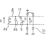
Will be in following explanation tenth embodiment of the invention.This tenth embodiment relates to a kind of structure, and this structure can guarantee that data are received in clamping under the situation of the nearly R/W of clamping unit.In above the 9th embodiment, the Q value step-down of the antenna resonance circuit when the nearly R/W of clamping unit in the card, consequently the delay of antenna resonance circuit becomes very little.In addition, because the modulating speed height of the transmitting antenna resonant circuit in the R/W unit, even phase change as shown in Figure 15 is detected in the position by alphabetical A indication, and this phase place trends towards changing as described in the 9th embodiment, phase place still changes prematurely, and reducing of amplitude consequently taken place again shown in letter b.Therefore, in the present embodiment, for fear of abnormal operation, the circuit structure that is adopted in by the 9th embodiment is once detect turning point is forbidden turning point in one period given time cycle afterwards detection.
Figure 16 simply illustrates the structure of the major part of card 10d in the present embodiment.Its basic structure is identical with the structure of Fig. 1.In Figure 16, test section 40 is to be used to detect turning point, and delay circuit 41 is to be used to cause postpone and forbid that a preset time detects turning point in the cycle after test section 40 detects turning point.Test section 40 and delay circuit 41 constitute phase change and detect inhibitor.The output of these parts by AND door 42 guiding control sections (17,17a).Even this structure makes that amplitude reduces once more after phase change detects, also can avoid the demodulation of unnecessary data, so although distance short also can be stable carry out Data Receiving.
Incidentally, Fig. 7,10 are based on simulation analysis of computer to 15.
Below the 11st embodiment of the present invention is described in conjunction with Figure 17, the figure shows the part of the structure of card.In this structure, used bridge rectifier circuit 5A as rectification circuit, the result is that the amplitude in the antenna resonance circuit 4 can be used as power source voltage, reaches the voltage in the half-wave voltage doubler that doubles Fig. 1.Because being transfused to signal is to double applied signal in the half-wave voltage doubler, if the card circuit is operated at 3V, pending signal is thought 1.5V between R/W unit and the card so.On the other hand, but because the operating voltage of the application receiving card circuit of bridge rectifier circuit 5A, i.e. 3V signal is so can realize that more accurate signal sends and reception.
Among Figure 17, be marked with identical label corresponding to the parts of the various embodiments described above.In this diagram, card comprises: the full-wave bridge rectifier circuit 5A that is made of to 5d rectifying device 5a; Phase inverter 30; The on-off circuit of forming by N type channel transistor 31a and 31d 31; Be used to obtain Zener (Zener) diode 33 of constant voltage source; Be used for the tank circuit of level and smooth rectified voltage with storage of electrical energy; And resistor R 1.Figure 18 A illustrates the voltage A between Figure 17 antenna resonance circuit 4 two ends, and Figure 18 B illustrates the output F (expression is not synchronous with voltage A) before the bridge rectifier circuit 5A.
Now the 12 embodiment is described referring to Figure 19.Figure 19 is the diagram of an example of a signal generating circuit, and the effectiveness of this circuit is to produce the switching signal through on-off circuit 31.The low voltage end of antenna resonance circuit 4 is by this circuit ground.In diagram, signal generating circuit is to be made of comparer 34 and D-D-flip flop 35.In addition, Figure 20 illustrates the waveform of Figure 17 and 19 circuit.Comparer 34 detects signal B input or that come in and becomes and be lower than by this fact of the earth level shown in the dotted line, then a signal paraphase, is grounded with the low voltage end of this antenna resonance circuit 4.This structure can make the low voltage end ground connection of antenna resonance circuit 4 and extract signal from its high voltage end.
Embodiment 13
Below the 13rd embodiment of the present invention is described.Present embodiment is to detect for the strong blocking statutes of the voltage fluctuation of the card that is received in order to realize, this voltage fluctuation is owing to the variation of the distance between R/W unit under the situation of carrying out the data transmission when phase modulation and the card is caused.The variation of phase place is based on amplitude and judges among the above embodiment, present embodiment is to obtain a reference phase signal by a phase-locked loop circuit in contrast, thereby with its with the signal that received on phase place relatively, the variation of phase place is as the function of the difference of phase place therebetween and detected.Thereby card can not be subjected to the influence of amplitude variations.
Figure 21 represents the formation of the test section that (for example, the left side of Figure 17 circuit) installed in the control section according to the card of present embodiment, and Figure 22 represents waveform wherein.Among Figure 21, include: a PLL (phase-locked loop circuit), EX-OR circuit 37 and D-D-flip flop 38a, 38b in the test section.Signal C and D for example can obtain from the circuit of Figure 19 among Figure 22.The test section comprises PLL36 and as the input signal received signal D to this PLL36, this signal indication input signal B becomes and is lower than this fact of ground level, test section generation one and the synchronous output signal D ' of input signal D then.This output signal D ' D-D-flip flop 38b be divided into 1/2 and generate a reference phase signal D ".EX-OR37 make to constitute reference phase signal D " with the 12 embodiment in the EX-OR of switching signal C, this EX-OR result is every half period sampling among the signal E by the output signal of PLL36 D-D-flip flop 38a shape, detects output E ' so generate.In passing, switching signal C on phase place corresponding to received signal.Switching signal C and reference phase signal D " EA-OR and sampling thereof at the interval of semiperiod can guarantee high-quality detection output.
Below describe with regard to the 14th embodiment of the present invention.Realize high-speed communication under the condition that the purpose of this embodiment is to be implemented in the R/W unit and to block certain program that is separated from each other.More specifically, in order to make the R/W unit, send data frequency (carrier wave) for being different to the R/W unit from card from the R/W unit to the frequency setting that the electric energy that is provided is provided when a side of card powers energy, receiving data continuously from clamping.Figure 23 illustrates the waveform that is presented under this situation.In the 12 embodiment, switching signal C is by paraphase, for example make as shown in Figure 20 as long as when the amplitude of the voltage waveform A between antenna resonant circuit 4 two ends passes through zero cross point (the anti-phase point of polarity), the low voltage end of antenna resonance circuit 4 and GND coupling, and its high voltage end is extracted as signal.On the other hand, in this 14 embodiment switching signal C be set to the time every a zero cross point rather than resemble Figure 23 by shown in the C at each zero cross point the time by paraphase.So, under the situation of switching signal at noninvert, before zero cross point, low voltage end and GND coupling, and the usefulness of the signal extraction of high voltage end, and after zero cross point, high voltage end ground connection and the low voltage end provides signal.In addition, high voltage end ground connection at this moment low voltage end produces a signal, and after the zero crossing low voltage end ground connection and the high voltage end generates signal.Signal from the high voltage end of antenna resonance circuit 4 is used for making the Vcc charging by bridge rectifier circuit 5A, and from the signal of its low voltage end by bridge rectifier circuit 5A by clamp (clamping) in GND-a (being lower than GND slightly).That is, Vcc repeats twice and at GND twice, the waveform of Chan Shenging is shown in F among Figure 23 like this by being clamped at of being realized of Zener diode 33.From Figure 24 obviously as seen, this waveform is identical with the composite wave M of reference frequency R, and frequency R/2 is 1/2 of reference frequency R.So can understand, the voltage A at antenna resonance circuit 4 two ends has comprised and has been used for the carrier wave that data send, and its frequency is 1/2 of an electric energy reception wave frequency.Point out that in passing the resistor R 1 among Figure 17 is what to be used to regulate from the intensity of the transmission carrier wave of card.
The switching signal that is installed in of trigger does not become when anti-phase by paraphase, and this signal of supposition EX-OR, same input signal in the time of can obtaining with acknowledge(ment) signal.Thereby owing to can obtain identical input signal with simple formation, so control circuit is easy to formation, and because carrier wave produces by ground connection, the result is less by the loss of the bag of rectification and storage energy.Also can use other method, for example use PLL, make grounding transistor (see the 31c among Figure 17,31d) conducting simultaneously.In addition, as described below, be used for carrier wave that data send be not limited to frequency be electric energy receive wave frequency 1/2, and the frequency of carrier wave can be set at electric energy receive wavelength-division frequently the electric energy of (dividing) gained receive 1/4,1/8 etc. of wave frequency.Even this situation also shows same effect.
The 15th embodiment of the present invention below is described.Present embodiment specifically is used for being implemented in the modulation of the carrier wave that 1 the 14 embodiment produced.In the 14 embodiment, the length of switching signal C is doubled when modulation as shown in figure 25, makes and modulates in the bi-phase shift keying mode.In other words, though the paraphase of switching signal is carried out every a zero cross point in the 14 embodiment, in the present embodiment, its paraphase be when modulation per four zero cross points shown in D among Figure 25 carry out.Figure 26 A illustrates the actual form of signal A, and Figure 26 B illustrates the actual form of signal F, and wherein D represents a modulated part.
By this structure, frequency is that the transmission carrier wave and the power of power-frequency 1/2 receives generation simultaneously, and resulting transmission carrier wave for example can be sent to R/W unit one side by phase modulation with these data.Similarly, be used for carrier wave that data send and be being not limited to power and receive 1/2 of wave frequency, the frequency of carrier wave also can be set at by power and receive 1/4,1/8 etc. of power reception wave frequency that the frequency division of ripple get.
Embodiment 16
And then the following explanation 16th embodiment of the present invention.Present embodiment proposes the further improvement than the data rate of top the 15 embodiment gained, and this is to realize by increasing a quantity of information in the signal.Among the 15 embodiment, switching signal C is that per four zero cross points of the voltage waveform between the two ends of antenna resonance circuit 4 once switch as shown in Figure 25, obtains the bi-phase shift keying mode therefrom in the above.On the other hand, in the present embodiment, in addition, switch at per three the zero cross point places of voltage waveform A as shown in Figure 27 A between the two ends of antenna resonance circuit, and and then carry out unseparated continuous switching as shown in Figure 27 B, consequently realized 0 ° of quadriphase PSK mode (four kinds of phase places :), 90 °, 180 °, go up phase modulation for 270 °).This quadriphase PSK mode is compared the information that twice can be provided with the bi-phase shift keying mode, so the data transmission speed is doubled.So this makes, and the data transmission speed doubles under same modulating speed (the transmission quantity of information that doubles).Point out that in passing embodiment 14 and 15 further development is possible.
Figure 28 to 32 has represented that the circuit that blocks among the 14 to 16 embodiment constitutes, wherein be set at and be different from data transmission frequency (carrier frequency), make data send to be that the phase modulation by bi-phase shift keying mode or quadriphase PSK mode is realized from the R/W unit to the power transmission frequency of card.In these diagrams, the formations of Figure 28 and 29 expression card circuit, wherein data send in the bi-phase shift keying mode and carry out (based on two class phases: 0 ° with 180 ° of phase modulation), and the carrier frequency of use is 1/2 power transmission frequency.In addition, Figure 30 represents that the card circuit constitutes, and by this circuit, it is that applying frequency is that the carrier wave of 1/2 power delivery frequency carries out in quadriphase PSK mode (based on 0 °, 90 °, 180 °, the phase modulation of 270 ° of four class phase) that data send.In addition, Figure 31 is a card circuit structure diagram, and this circuit is used for carrying out data in the bi-phase shift keying mode and sends, and used carrier frequency is 1/4 of a power transmission frequency.Figure 32 is the diagram that a card circuit constitutes again, is used for carrying out data in the quadriphase PSK mode and sends, and the carrier frequency of using is 1/4 of the power transmission frequency.
Among Figure 28 to 32, be marked with identical label, label 301 to 305 expression D-D-flip flops corresponding to the parts of the foregoing description, label 310,311 expression EX-OR circuit, number 320 to 329 expression OR door or NOR doors, numbers 340 to 344 expression AND door or NAND doors, number 360 to 362 expression phase inverters.
The circuit of Figure 28 at first, is described.This circuit carries out sending with the data of bi-phase shift keying mode, and its used carrier frequency is 1/2 of a power transmission frequency.A PLL36, EX-OR circuit 37 and D-D- flip flop 38a, 38b has constituted a demodulator circuit, i.e. receiving circuit (seeing Figure 21).In addition, comparer 34, EX-OR circuit 310,311, OR door 320 to 323, and D-D-flip flop 301 to 303 unites when receiving and produces normal switch signal C (seeing Figure 19 and 20), and when transmission, using 301 pairs of power transmission frequency of D-D-flip flop to carry out frequency division is 1/2, produces the carrier wave (carrier wave has 1/2 frequency of power transmission frequency) of 1/2 frequency.Make according to a signal, promptly, carry out the modulation of bi-phase shift keying mode from the transmission data of AND door 340.
When receiving, the transmission/reception switching signal that be input to OR door 321 becomes the level state for L, and the D-D-flip flop enters a stationary state of not carrying out frequency division.On the other hand, when sending, this signal transfers the H level state to, and D-D-flip flop 301 is 1/2 with the power-frequency frequency division as a result, the feasible carrier wave that produces the 1/2-frequency.After this, this carrier wave is modulated according to the signal of sending from AND door 340 as sending data in the bi-phase shift keying mode.This AND door 340 sends a signal, and this signal is that the response timing signal obtains by the gate (gating) of inverted image signal to the transmission data.
Below describe with the 33B pair of effect relevant referring to Figure 33 A with D-D-flip flop 302.Figure 33 A expresses the output D of comparer 34, the output U of D-D-flip flop 302, the output D1 of EX-OR circuit 310 and the switching signal when receiving, and Figure 33 B expresses the output D of comparer 34, the output U of D-D-flip flop 302, the output D1 of EX-OR circuit 310 and the switching signal when sending.To the power frequency division that is used to send frequently the time, D-D-flip flop 302 generates signal U, this signal paraphase when not paraphase of switching signal.EX-OR circuit 310 is carried out the EX-OR function to the scale-of-two output of signal U and comparer 34, so obtain signal D1, no matter whether this signal signal D when receiving and send changes can not change.The effect of this signal D1 is as an input signal to PLL 36.When Data Receiving, switching signal is handled as the signal of expression carrier phase, and it is sent the effect of carrier wave when data send, and the result is that this circuit may form the existence whether error to received data.For this reason, be to output to the demodulator circuit that comprises PLL 36 by the signal D1 of EX-OR gained of signal U and the signal D of expression switching signal, can avoid when sending receiving the erroneous judgement of data with this.
As the circuit of Figure 28, Figure 29 circuit carries out data in the bi-phase shift keying mode and sends, and frequency of utilization is 1/2 a carrier wave of power transmission frequency.This circuit and difference are to comprise the part of following device: phase inverter 360, NAND door 341, NOR door 324, D-D-flip flop 304 and OR door 325, this part, with the timing to the output Q value of the output D1 of EX-OR circuit 310 and D-D-flip flop 301 is purpose, produces a signal that is used to modulate.Other the operation circuit with Figure 28 basically is identical.Thereby the circuit of Figure 28 does not have to consider the timing (result is this problem) to modulation, but the circuit of Figure 29 is with respect to the output of EX-OR circuit 310, the timing of the output of D-D-flip flop 301 etc.
In addition, the circuit design of Figure 30 is for to carry out the transmission of data in the quadriphase PSK mode, and frequency of utilization is 1/2 a carrier wave of power-frequency.The circuit that this circuit is different from Figure 28 and 29 is to comprise the part of following device: OR door 325,326, phase inverter 360,362, AND door 342 to 344, NOR door 324,327, and D-D-flip flop 304, this part produces carries out the signal modulated in the quadriphase PSK mode.Use this structure, have four kinds of phase modulation reality available: 0 ° of phase place, when no signal; 90 ° of phase places, when pi/2 one delay signal is set at the H level, 180 ° of phase places are when reversed phase signal is set at the H level; And 270 ° of phase places, when the pi/2 anticipating signal is set at the H level.
And, Figure 31 circuit design sends for carry out data in the bi-phase shift keying mode, uses the carrier wave of its frequency as power frequency 1/4, wherein two D-D-flip flops 301,305 installing is in order to produce 1/4 the carrier wave that its frequency is a power-frequency, and the part among other parts and Figure 28 is basic identical.In addition, the circuit reality of Figure 32 realize the transmission of data with the strong prosecutor formula of four phase shifts, use the carrier wave of its frequency as power-frequency 1/4, and characteristics with Figure 30 circuit of the data transmission of depending on the quadriphase PSK mode, and having the characteristics of Figure 31 circuit simultaneously, the frequency that this circuit produces carrier wave is 1/4 of a power-frequency.
Embodiment 17
Below will describe the 17th embodiment of the present invention.In the 3rd embodiment, output capacitor 11 is to be connected in the semiperiod that is used for phase modulation with antenna resonance circuit 4, and in the 7th embodiment, the two ends of the transmitting antenna resonant circuit 201 among R/W unit one side the semiperiod that is used for phase modulation by short circuit.On the other hand, in this 17 embodiment, comprised as in blocking among 13 embodiment-PLL 36 (seeing Figure 21), made the length of semiperiod obtain based on the output of PLL 36.So modulation has consequently been finished by short circuit in the two ends of antenna resonance circuit 4.Figure 34 illustrates the circuit structure according to the card of present embodiment, and Figure 35 illustrates the waveform in this circuit.Output transistor 9 short circuit antenna resonance circuits 4 to be to realize the bi-phase shift keying mode during semiperiod in modulation after the zero cross point, and the semiperiod is based on the output of PLL 36 and found before this.So, can carry out without output capacitor 11 in side's modulation of card.
Embodiment 18
Below so the explanation 18th embodiment of the present invention.In the 9th embodiment, the decline of amplitude that the data turning point is based on card one side's antenna resonance circuit is detected, and to the result that should detect, it is 1/2 that output capacitor 11 is coupled to set resonance frequency with resonant circuit 4 during the semiperiod, so force to carry out demodulation.On the other hand, in this 18 embodiment, at the two ends of antenna resonance circuit 4 by short circuit with before realizing the high speed demodulation as in the 13 embodiment one by one PLL 36 (seeing Figure 21) inserted card, thereby obtain the length of semiperiod based on the output of PLL 36.
Figure 36 A is the diagram of the circuit structure of the card in the present embodiment, and Figure 36 B represents comparer, the level that is used to detect the amplitude of resonant circuit 4 such fact that descends, and Figure 36 C represents the waveform of this circuit.In the present embodiment, the output that the semiperiod is based on PLL 36 obtains, and output transistor 9 when resonant circuit 4 amplitude levels reduce during the semiperiod short circuit antenna resonance circuit 4, thereby finish the high speed demodulation.This structure does not need to export brilliant pipe 11 and is used for the high speed demodulation, and what need only is two, promptly is used for the comparer of the detection that zero cross point and amplitude reduce.Comparer 16a is the level that is used for detecting antenna resonance circuit 4 to 16c.
Embodiment 19
Below the 19th embodiment of the present invention is described.Present embodiment has realized generating its frequency for receiving the transmission carrier wave of wave frequency 1/2, has used the phase modulation circuit based on the output capacitor described in the 3rd embodiment or the 9th embodiment.The circuit that Figure 38 illustrates card constitutes, and Figure 39 represents the waveform in Figure 38 circuit formation.In the present embodiment, output transistor 9 is in by break-make to be controlled, make and be set to one-period with the item that is connected to output capacitor 11 as shown in 39 as Figure 38, and be set at two cycles to the disconnected of this capacitor, consequently to have produced its frequency be the transmission carrier wave of 1/2 power-frequency to this circuit.This makes that sending carrier wave can receive generation simultaneously with power.
Figure 40 A is card one side of present embodiment or the diagram of the waveform among R/W unit one side to 40C, and these diagrams get from simulation analysis of computer.In these diagrams, Figure 40 A represents card one side's waveform (corresponding to the A among Figure 39).Figure 40 B represents the waveform of the reception among R/W unit one side, and Figure 40 C represents the filtered resulting signal waveform of signal as Figure 40 B.From Figure 40 C obviously as seen, can be provided as the frequency of 1/2 power-frequency.
At last in the following explanation 20th embodiment of the present invention.The characteristics of present embodiment are that the structure of using the 19 embodiment realizes modulation.In the circuit of Figure 38, be set at one-period to the disconnected of output capacitor 11 when the modulation as shown in Figure 41, this can the bi-phase shift keying mode realize modulation.Figure 42 A represents in the present embodiment card or R/W unit one side's waveform to 42C, and these waveforms are according to simulation analysis of computer.Figure 42 A represents the waveform (corresponding to the A among Figure 41) among card one side.Figure 42 represents the waveform that R/W unit one side is received, and Figure 42 C represents by to the resulting waveform of Figure 42 B signal filtering.Can see by the modulating part shown in the A Figure 42 A from these diagrams and to have stipulated appearance by the part shown in the B among Figure 42 C.
Should be appreciated that the above preferred embodiment of the present invention that only relates to, this is to be used for all changes and the modification of described purpose embodiments of the present invention in order to try hard to letter lid, and these do not deviate from the spirit and scope of the present invention.
Claims (9)
1. a non-contact IC card is used electromagnetic wave and is not also wherein contained battery as communication medium, and it comprises:
Antenna resonance circuit is used for data and sends and receive;
The incoming level detecting device, it is connected with antenna resonance circuit by rectification circuit, comprises a comparer, is used for received signal level after the rectification circuit rectification and predetermined value are compared; And
The quality factor regulator, comprise a variable resistor device that is connected with above-mentioned antenna resonance circuit, when the voltage after above-mentioned detecting device detects rectification surpassed predetermined value, this variable resistor device was conditioned to change the quality factor of above-mentioned antenna resonance circuit according to plussage.
2. according to the non-contact IC card of claim 1, also comprise:
Phase detectors are used to detect for the antenna resonance circuit free-running phase place of data transmission with the usefulness of reception; And
The energy feeder is used for that the free-running phase place with above-mentioned antenna provides energy from a tank circuit to above-mentioned antenna resonance circuit when sending.
3. according to the non-contact IC card of claim 1, also comprise:
The resonance frequency switch, be used for a capacitor being inserted above-mentioned antenna resonance circuit and disconnecting this capacitor from it according to one of the variation of output data and this output data and output of above-mentioned phase detectors, so that change the resonance frequency of above-mentioned antenna resonance circuit
Wherein, data send and to be based on that one of frequency modulation and phase modulation carry out.
4. according to a kind of non-contact IC card of claim 3, and then comprise phase regulator, be used for the phase adjusted of the voltage that induces because of the signal that is received at above-mentioned antenna resonance circuit to the free-running phase place of above-mentioned resonant circuit.
5. according to the non-contact IC card of claim 4, also comprise phase change and detect inhibitor, being used for given time cycle after the detection of a phase-detection is carried out forbids detection to phase change signal amplitude being descended by demodulation.
6. according to the non-contact IC card of claim 3, wherein above-mentioned capacitor be connected with above-mentioned antenna resonance circuit during the one-period and during two cycles with its disconnection, the frequency setting that is used to send is to be used for 1/2 of frequency that electric energy supplies with, and sends and carry out under the electric energy accepting state.
7. according to the non-contact IC card of claim 6, wherein above-mentioned capacitor disconnects from above-mentioned antenna resonance circuit during one-period, and the phase modulation that is used to send.
8. according to the non-contact IC card of claim 1, use electromagnetic wave and also wherein do not contain battery as communication medium, it comprises
The phase change detecting device is used for detecting because the confession data that the signal of being received causes send and the phase change of the antenna resonance circuit voltage of the usefulness of reception based on its oscillation amplitude change; And
Detuner, the phase change that is used for being detected according to above-mentioned phase change detecting device is to the data demodulation.
9. non-contact IC card according to Claim 8 also comprises phase regulator, is used for above-mentioned antenna resonance circuit because of the phase adjusted of the voltage of the induction of signal the received phase place to this resonant circuit vibration.
Applications Claiming Priority (12)
| Application Number | Priority Date | Filing Date | Title |
|---|---|---|---|
| JP243097/94 | 1994-10-06 | ||
| JP24309794 | 1994-10-06 | ||
| JP243097/1994 | 1994-10-06 | ||
| JP307834/1994 | 1994-12-12 | ||
| JP307834/94 | 1994-12-12 | ||
| JP30783494 | 1994-12-12 | ||
| JP14781795 | 1995-06-14 | ||
| JP147817/1995 | 1995-06-14 | ||
| JP147817/95 | 1995-06-14 | ||
| JP244738/1995 | 1995-09-22 | ||
| JP7244738A JPH0962816A (en) | 1994-10-06 | 1995-09-22 | Non-contact ic card and non-contact ic card system including the same |
| JP244738/95 | 1995-09-22 |
Publications (2)
| Publication Number | Publication Date |
|---|---|
| CN1143227A CN1143227A (en) | 1997-02-19 |
| CN1111299C true CN1111299C (en) | 2003-06-11 |
Family
ID=27472810
Family Applications (1)
| Application Number | Title | Priority Date | Filing Date |
|---|---|---|---|
| CN95117764A Expired - Fee Related CN1111299C (en) | 1994-10-06 | 1995-10-06 | Non-contact IC card and non-contact IC card system |
Country Status (7)
| Country | Link |
|---|---|
| US (4) | US5698838A (en) |
| EP (1) | EP0706151B1 (en) |
| JP (1) | JPH0962816A (en) |
| KR (1) | KR100223989B1 (en) |
| CN (1) | CN1111299C (en) |
| DE (1) | DE69532399T2 (en) |
| TW (1) | TW324868B (en) |
Families Citing this family (152)
| Publication number | Priority date | Publication date | Assignee | Title |
|---|---|---|---|---|
| JPH0981701A (en) * | 1995-09-19 | 1997-03-28 | Toshiba Corp | Noncontact type information recording medium and noncontact type information transmitting method |
| JP3205260B2 (en) * | 1996-04-30 | 2001-09-04 | 株式会社山武 | Non-contact data transmission / reception method and device |
| DE19629646C2 (en) * | 1996-07-23 | 1998-09-10 | Wolf Gmbh Richard | Method and device for the automatic identification of components of medical device systems |
| JP3392016B2 (en) * | 1996-09-13 | 2003-03-31 | 株式会社日立製作所 | Power transmission system and power transmission and information communication system |
| US5949823A (en) * | 1996-09-13 | 1999-09-07 | Hitachi, Ltd. | Data communication system and radio IC card system |
| SG54559A1 (en) | 1996-09-13 | 1998-11-16 | Hitachi Ltd | Power transmission system ic card and information communication system using ic card |
| JPH10187916A (en) * | 1996-12-27 | 1998-07-21 | Rohm Co Ltd | Responder for contactless ic card communication system |
| US5930304A (en) * | 1997-03-20 | 1999-07-27 | Motorola, Inc. | Wireless powered communication device with adaptive data detection and method |
| US6164532A (en) * | 1997-05-15 | 2000-12-26 | Hitachi, Ltd. | Power transmission system, power transmission/communication system and reader and/or writer |
| US6176433B1 (en) * | 1997-05-15 | 2001-01-23 | Hitachi, Ltd. | Reader/writer having coil arrangements to restrain electromagnetic field intensity at a distance |
| JPH10320519A (en) | 1997-05-19 | 1998-12-04 | Rohm Co Ltd | Responder in ic card communication system |
| US6747548B1 (en) | 1997-06-18 | 2004-06-08 | Mitsubishi Denki Kabushiki Kaisha | Non-contact IC card system and non-contact IC card |
| DE69838364T2 (en) | 1997-06-20 | 2008-05-29 | Hitachi Kokusai Electric Inc. | Read / write device, power supply system and communication system |
| JPH1166248A (en) * | 1997-08-12 | 1999-03-09 | Mitsubishi Electric Corp | Non-contact type ic card |
| FR2768875B1 (en) * | 1997-09-23 | 2000-06-02 | Sgs Thomson Microelectronics | RADIO FREQUENCY SIGNAL DETECTOR FOR CONTACTLESS CHIP CARD |
| GB2330957B (en) * | 1997-11-01 | 2002-06-05 | Motorola Inc | Power supply clamp and method in a smartcard |
| US6211799B1 (en) * | 1997-11-06 | 2001-04-03 | Massachusetts Institute Of Technology | Method and apparatus for transbody transmission of power and information |
| EP1163630A4 (en) * | 1998-01-23 | 2002-07-31 | Motorola Inc | Portable data device and method of switching between a power and data mode of operation |
| AU2259699A (en) | 1998-01-29 | 1999-08-16 | Magellan Technology Pty Limited | A transceiver |
| US8108307B1 (en) | 1998-03-30 | 2012-01-31 | Citicorp Development Center, Inc. | System, method and apparatus for value exchange utilizing value-storing applications |
| EP0949593A2 (en) | 1998-03-30 | 1999-10-13 | Citicorp Development Center | System, method and apparatus for value exchange utilizing value-storing apparatus |
| US6169475B1 (en) | 1998-03-30 | 2001-01-02 | Xircom, Inc. | System and method for active detection of connection to a network |
| FR2776865B1 (en) * | 1998-03-31 | 2000-05-05 | Commissariat Energie Atomique | INDUCTIVE COUPLING TELETRANSMISSION DEVICE |
| FR2778521B1 (en) | 1998-05-06 | 2000-06-16 | Sgs Thomson Microelectronics | BPSK ENCODER CIRCUIT |
| FR2780221B1 (en) | 1998-06-22 | 2000-09-29 | Sgs Thomson Microelectronics | TRANSMISSION OF AN OPERATING INSTRUCTION BY AN ALTERNATIVE POWER SUPPLY LINE |
| FR2780220A1 (en) | 1998-06-22 | 1999-12-24 | Sgs Thomson Microelectronics | TRANSMISSION OF DIGITAL DATA ON AN ALTERNATIVE POWER LINE |
| DE19827691C1 (en) * | 1998-06-22 | 2000-01-13 | Skidata Ag | Method for communication between contactless data carriers and end devices |
| FR2781074B1 (en) * | 1998-07-08 | 2006-04-28 | Commissariat Energie Atomique | ANALOG INTERFACE FOR AUTONOMOUS INFORMATION EXCHANGE CIRCUIT |
| US6173897B1 (en) * | 1998-07-27 | 2001-01-16 | John W. Halpern | Universal card interface module for contact free cards |
| CN1326085C (en) * | 1998-07-31 | 2007-07-11 | 松下电器产业株式会社 | Portable body used in two way, communication system, communication method, terminal, computer-readable recorded medium on which program is recorded |
| JP3649374B2 (en) * | 1998-11-30 | 2005-05-18 | ソニー株式会社 | Antenna device and card-like storage medium |
| FR2787260B1 (en) * | 1998-12-09 | 2003-01-24 | Gemplus Card Int | ELECTRONIC CONTACTLESS COMMUNICATION DEVICE WITH OPTIONAL AUXILIARY ENERGY SOURCE |
| TW484101B (en) * | 1998-12-17 | 2002-04-21 | Hitachi Ltd | Semiconductor device and its manufacturing method |
| AU1765500A (en) * | 1998-12-23 | 2000-07-31 | Corporation Hypersecur Inc. | Transceiver interface with selective secure and insecure data exchange modes |
| EP1030266B1 (en) * | 1999-02-19 | 2009-05-06 | Nippon Telegraph and Telephone Corporation | Noncontact type IC card and system therefor |
| JP3494067B2 (en) * | 1999-03-19 | 2004-02-03 | 日本電信電話株式会社 | Base station communication device and power supply method for portable wireless communication device |
| FR2792135B1 (en) | 1999-04-07 | 2001-11-02 | St Microelectronics Sa | VERY CLOSE COMPLAGE OPERATION OF AN ELECTROMAGNETIC TRANSPONDER SYSTEM |
| US6650226B1 (en) * | 1999-04-07 | 2003-11-18 | Stmicroelectronics S.A. | Detection, by an electromagnetic transponder reader, of the distance separating it from a transponder |
| FR2792134B1 (en) | 1999-04-07 | 2001-06-22 | St Microelectronics Sa | DISTANCE DETECTION BETWEEN AN ELECTROMAGNETIC TRANSPONDER AND A TERMINAL |
| FR2792132B1 (en) | 1999-04-07 | 2001-11-02 | St Microelectronics Sa | READING TERMINAL OF AN ELECTROMAGNETIC TRANSPONDER OPERATING IN VERY CLOSE COUPLING |
| FR2792136B1 (en) | 1999-04-07 | 2001-11-16 | St Microelectronics Sa | DUPLEX TRANSMISSION IN AN ELECTROMAGNETIC TRANSPONDER SYSTEM |
| FR2792130B1 (en) | 1999-04-07 | 2001-11-16 | St Microelectronics Sa | ELECTROMAGNETIC TRANSPONDER WITH VERY CLOSE COUPLING OPERATION |
| US6659352B1 (en) * | 1999-06-02 | 2003-12-09 | Matsushita Electric Industrial Co., Ltd. | Semiconductor integrated circuit, a contactless information medium having the semiconductor integrated circuit, and a method of driving the semiconductor integrated circuit |
| FR2795891B1 (en) * | 1999-07-01 | 2007-04-20 | France Telecom | MICRO-ELECTRONIC COMPONENT INTEGRATING ASYNCHRONOUS DIGITAL PROCESSING MEANS AND AN ELECTROMAGNETIC CONTACTLESS COUPLING INTERFACE |
| US6134130A (en) * | 1999-07-19 | 2000-10-17 | Motorola, Inc. | Power reception circuits for a device receiving an AC power signal |
| US7049935B1 (en) | 1999-07-20 | 2006-05-23 | Stmicroelectronics S.A. | Sizing of an electromagnetic transponder system for a dedicated distant coupling operation |
| FR2796781A1 (en) * | 1999-07-20 | 2001-01-26 | St Microelectronics Sa | DIMENSIONING OF AN ELECTROMAGNETIC TRANSPONDER SYSTEM FOR HYPERPROXIMITY OPERATION |
| JP3824451B2 (en) * | 1999-07-29 | 2006-09-20 | 富士通株式会社 | Non-contact IC card presence / absence detection circuit |
| EP1087332B1 (en) * | 1999-09-22 | 2008-02-13 | EM Microelectronic-Marin SA | Transponder constructed for several different applications |
| ATE386309T1 (en) | 1999-09-22 | 2008-03-15 | Em Microelectronic Marin Sa | TRANSPONDER FOR DIFFERENT PURPOSES |
| JP4823458B2 (en) | 1999-10-22 | 2011-11-24 | エヌエックスピー ビー ヴィ | Data carrier with load modulation means and improved power supply in load modulation process |
| DE59913798D1 (en) * | 1999-12-16 | 2006-10-05 | Infineon Technologies Ag | Chip card with two demodulation devices |
| FR2804557B1 (en) * | 2000-01-31 | 2003-06-27 | St Microelectronics Sa | ADAPTING THE TRANSMISSION POWER OF AN ELECTROMAGNETIC TRANSPONDER DRIVE |
| ATE396458T1 (en) * | 2000-03-22 | 2008-06-15 | Infineon Technologies Ag | CHIP CARD |
| CN1255759C (en) * | 2000-05-05 | 2006-05-10 | 皇家菲利浦电子有限公司 | Data carrier having means for changing resonant frequency of its resonant circuit |
| FR2808946A1 (en) | 2000-05-12 | 2001-11-16 | St Microelectronics Sa | VALIDATION OF THE PRESENCE OF AN ELECTROMAGNETIC TRANSPONDER IN THE FIELD OF A READER |
| FR2808941B1 (en) | 2000-05-12 | 2002-08-16 | St Microelectronics Sa | VALIDATION OF THE PRESENCE OF AN ELECTROMAGNETIC TRANSPONDER IN THE FIELD OF AN AMPLITUDE DEMODULATION READER |
| FR2808942B1 (en) * | 2000-05-12 | 2002-08-16 | St Microelectronics Sa | VALIDATION OF THE PRESENCE OF AN ELECTROMAGNETIC TRANSPONDER IN THE FIELD OF A PHASE DEMODULATION READER |
| FR2808945B1 (en) | 2000-05-12 | 2002-08-16 | St Microelectronics Sa | EVALUATION OF THE NUMBER OF ELECTROMAGNETIC TRANSPONDERS IN THE FIELD OF A READER |
| FR2809251B1 (en) * | 2000-05-17 | 2003-08-15 | St Microelectronics Sa | DEVICE FOR PRODUCING AN ELECTROMAGNETIC FIELD FOR A TRANSPONDER |
| FR2809235A1 (en) * | 2000-05-17 | 2001-11-23 | St Microelectronics Sa | ANTENNA FOR GENERATING AN ELECTROMAGNETIC FIELD FOR TRANSPONDER |
| FR2812986B1 (en) * | 2000-08-09 | 2002-10-31 | St Microelectronics Sa | DETECTION OF AN ELECTRIC SIGNATURE OF AN ELECTROMAGNETIC TRANSPONDER |
| US20030169169A1 (en) | 2000-08-17 | 2003-09-11 | Luc Wuidart | Antenna generating an electromagnetic field for transponder |
| JP3818045B2 (en) * | 2000-10-20 | 2006-09-06 | 株式会社日立製作所 | Ticket machine |
| KR100540890B1 (en) * | 2000-12-22 | 2006-01-10 | 한국전자통신연구원 | Contactless IC Card Reader of Contactless IC Card System |
| FR2820532A1 (en) * | 2001-02-02 | 2002-08-09 | Tagproduct | Non-contact communication with an electronic ticket, uses adaptive resonance emitter which responds to perturbation caused by presence of electronic ticket and alters coupling factor between sender and ticket |
| DE10162310A1 (en) * | 2001-12-19 | 2003-07-03 | Philips Intellectual Property | Method for signal transmission e.g. for small computers in credit card format, signal transmission takes place via smart card controller |
| WO2003065302A1 (en) * | 2002-02-01 | 2003-08-07 | Koninklijke Philips Electronics N.V. | Adapting coil voltage of a tag to field strength |
| FR2835946A1 (en) * | 2002-02-11 | 2003-08-15 | St Microelectronics Sa | ELECTROMAGNETIC TRANSPONDER WITH PROGRAMMABLE CODE |
| US6906612B2 (en) * | 2002-04-11 | 2005-06-14 | Lear Corporation | System and method for vehicle passive entry having inside/outside detection |
| JP2004132890A (en) * | 2002-10-11 | 2004-04-30 | Fujitsu Component Ltd | Noncontact ic card reader/writer apparatus, noncontact ic card, input apparatus, and noncontact method for computing position of ic card |
| US6882236B2 (en) * | 2002-11-05 | 2005-04-19 | Magneto-Inductive Systems Limited | Dynamically tuned amplifier for frequency shift keyed signals |
| JP2004166384A (en) * | 2002-11-12 | 2004-06-10 | Sharp Corp | Non-contact power feeding system, electromagnetic coupling characteristic adjustment method therein and power feeder |
| JP4564239B2 (en) * | 2003-04-11 | 2010-10-20 | オリンパス株式会社 | Endoscope device |
| JP4104502B2 (en) * | 2003-07-25 | 2008-06-18 | アルプス電気株式会社 | Passive keyless entry device |
| EP1667336B1 (en) * | 2003-09-19 | 2013-05-01 | Brother Kogyo Kabushiki Kaisha | Radio tag reader/writer |
| JP2005117153A (en) * | 2003-10-03 | 2005-04-28 | Toshiba Corp | Wireless communication apparatus, wireless communication method, and wireless communication medium |
| WO2005073904A1 (en) * | 2004-01-30 | 2005-08-11 | Semiconductor Energy Laboratory Co., Ltd. | Semiconductor device |
| JP4392256B2 (en) * | 2004-02-05 | 2009-12-24 | 株式会社ルネサステクノロジ | Semiconductor integrated circuit device and non-contact type IC card |
| JP2005229512A (en) * | 2004-02-16 | 2005-08-25 | Seiko Epson Corp | Data communication system, data communication device, non-contact communication medium, and data communication device control program |
| DE102004014203B4 (en) * | 2004-03-23 | 2006-02-02 | Infineon Technologies Ag | Contactless data carrier with current demodulation |
| KR100663376B1 (en) * | 2004-07-23 | 2007-01-02 | 주식회사 모팩소프트 | A wireless communication device and method |
| GB2465298B (en) * | 2004-09-24 | 2010-06-30 | Vision Rt Ltd | Image processing system for use with a patient positioning device |
| FR2879382A1 (en) * | 2004-12-14 | 2006-06-16 | St Microelectronics Sa | ERROR DETECTION IN AN AMPLITUDE MODULATION SIGNAL |
| US7490817B2 (en) * | 2005-01-04 | 2009-02-17 | Bfs Diversified Products Llc | Distance indicating system and method |
| KR20070116168A (en) * | 2005-03-30 | 2007-12-06 | 엔엑스피 비 브이 | Integrated circuit providing an external switching functionality |
| WO2006115196A1 (en) * | 2005-04-22 | 2006-11-02 | Daifuku Co., Ltd. | Secondary-side power receiving circuit of noncontact power supplying equipment |
| US7364144B2 (en) * | 2005-04-27 | 2008-04-29 | Bfs Diversified Products, Llc | Sensing and communication system and method |
| DE102005020101A1 (en) * | 2005-04-29 | 2007-01-25 | Giesecke & Devrient Gmbh | Portable data carrier and method for operating a portable data carrier |
| CN101189624A (en) * | 2005-05-23 | 2008-05-28 | Nxp股份有限公司 | Electronic communication system, in particular authentication control system, as well as corresponding method |
| FR2890207B1 (en) * | 2005-08-23 | 2007-11-02 | Inside Contactless Sa | INDUCTIVE COUPLING READER COMPRISING MEANS FOR EXTRACTING AN ELECTRIC POWER SUPPLY VOLTAGE |
| DE102005044194B4 (en) * | 2005-09-09 | 2007-11-15 | Infineon Technologies Ag | Measuring device and method for measuring relative phase angles of digital signals |
| JP2007094886A (en) * | 2005-09-29 | 2007-04-12 | Keyence Corp | Radio tag reader/writer, and radio tag read/write method |
| US7420462B2 (en) * | 2006-01-23 | 2008-09-02 | Bfs Diversified Products, Llc | Air spring distance indicating system and method |
| US8120465B2 (en) * | 2006-02-01 | 2012-02-21 | Vitaly Drucker | RFID tag, interrogator and system with improved symbol encoding and decoding |
| US7733239B2 (en) * | 2006-05-08 | 2010-06-08 | Bfs Diversified Products, Llc | Distance determining system and method |
| CN101149816B (en) * | 2006-09-20 | 2010-05-26 | 鸿富锦精密工业(深圳)有限公司 | Passive radio frequency identification chip with high intensity magnetic field protection function |
| JP2008104295A (en) * | 2006-10-19 | 2008-05-01 | Voltex:Kk | Non-contact power supply unit |
| JP5325415B2 (en) * | 2006-12-18 | 2013-10-23 | 株式会社半導体エネルギー研究所 | Semiconductor device |
| US9774086B2 (en) | 2007-03-02 | 2017-09-26 | Qualcomm Incorporated | Wireless power apparatus and methods |
| US7554473B2 (en) * | 2007-05-02 | 2009-06-30 | Cirrus Logic, Inc. | Control system using a nonlinear delta-sigma modulator with nonlinear process modeling |
| DE602008002596D1 (en) | 2007-05-30 | 2010-10-28 | Nxp Bv | RFID DEVICE, RFID SYSTEM AND SIGNAL DISTORTION |
| US9124120B2 (en) | 2007-06-11 | 2015-09-01 | Qualcomm Incorporated | Wireless power system and proximity effects |
| JP4488040B2 (en) | 2007-07-26 | 2010-06-23 | Tdk株式会社 | Radio communication transmitter / receiver, RFID system, and radio communication transmitter / receiver reception method |
| JP4285576B1 (en) * | 2007-12-04 | 2009-06-24 | オムロン株式会社 | Non-contact IC medium communication apparatus and method, and program thereof |
| US8576589B2 (en) | 2008-01-30 | 2013-11-05 | Cirrus Logic, Inc. | Switch state controller with a sense current generated operating voltage |
| ITMO20080053A1 (en) * | 2008-02-29 | 2009-09-01 | Alma Mater Studiorum Uni Di Bologna | METHOD AND APPARATUS FOR COMMUNICATION IN ULTRA-BROADBAND RFID SYSTEMS |
| EP2279484B1 (en) | 2008-05-19 | 2011-10-12 | Nxp B.V. | Rfid transponder |
| US8222872B1 (en) * | 2008-09-30 | 2012-07-17 | Cirrus Logic, Inc. | Switching power converter with selectable mode auxiliary power supply |
| EP2335315B1 (en) * | 2008-10-09 | 2016-09-07 | Nxp B.V. | Antenna with a controllable switching element connecting two antenna portions |
| JP4668315B2 (en) * | 2008-12-02 | 2011-04-13 | フェリカネットワークス株式会社 | Information processing apparatus, communication control method, and program |
| SI23044A (en) * | 2009-04-14 | 2010-10-29 | Ids D.O.O. | Procedure and circuit for amplitude modulation of carrier signal withrequired modulation factor |
| JP5278197B2 (en) * | 2009-06-29 | 2013-09-04 | ソニー株式会社 | Non-contact communication device and non-contact communication method |
| US9178415B1 (en) | 2009-10-15 | 2015-11-03 | Cirrus Logic, Inc. | Inductor over-current protection using a volt-second value representing an input voltage to a switching power converter |
| US8487591B1 (en) | 2009-12-31 | 2013-07-16 | Cirrus Logic, Inc. | Power control system with power drop out immunity and uncompromised startup time |
| US8313028B2 (en) | 2010-02-17 | 2012-11-20 | On Track Innovations Ltd. | Multiple antenna reading system suitable for use with contactless transaction devices |
| US8195236B2 (en) | 2010-06-16 | 2012-06-05 | On Track Innovations Ltd. | Retrofit contactless smart SIM functionality in mobile communicators |
| US8729811B2 (en) | 2010-07-30 | 2014-05-20 | Cirrus Logic, Inc. | Dimming multiple lighting devices by alternating energy transfer from a magnetic storage element |
| US8866452B1 (en) | 2010-08-11 | 2014-10-21 | Cirrus Logic, Inc. | Variable minimum input voltage based switching in an electronic power control system |
| US9510401B1 (en) | 2010-08-24 | 2016-11-29 | Cirrus Logic, Inc. | Reduced standby power in an electronic power control system |
| US8424757B2 (en) | 2010-12-06 | 2013-04-23 | On Track Innovations Ltd. | Contactless smart SIM functionality retrofit for mobile communication device |
| JP5844631B2 (en) * | 2010-12-15 | 2016-01-20 | 東海旅客鉄道株式会社 | Power receiving device and power receiving method |
| JP5597145B2 (en) * | 2011-02-08 | 2014-10-01 | ルネサスエレクトロニクス株式会社 | Power transmission equipment |
| CN103636109B (en) | 2011-06-03 | 2016-08-17 | 塞瑞斯逻辑公司 | For operating method and apparatus and the electric power distribution system of switched power transducer |
| WO2012167161A1 (en) | 2011-06-03 | 2012-12-06 | Cirrus Logic, Inc. | Primary-side control of a switching power converter with feed forward delay compensation |
| JP5834655B2 (en) * | 2011-09-09 | 2015-12-24 | ソニー株式会社 | Transmission device, transmission / reception device, and integrated circuit |
| CN103959601B (en) * | 2011-09-29 | 2019-11-01 | Lg伊诺特有限公司 | Wireless power transmitter, wireless power receiver and impedance adjustment |
| DE102011115721B4 (en) * | 2011-10-12 | 2022-02-03 | Fraunhofer-Gesellschaft zur Förderung der angewandten Forschung e.V. | System for wireless energy transfer |
| CN102364500B (en) * | 2011-10-18 | 2015-07-29 | 山东华翼微电子技术股份有限公司 | Passive RFID or contact type intelligent card chip dynamic frequency scalable circuit |
| DK2775616T3 (en) * | 2011-11-25 | 2019-11-11 | Oticon As | HF transmitter for electric short antenna |
| WO2013090777A2 (en) | 2011-12-14 | 2013-06-20 | Cirrus Logic, Inc. | Isolation of secondary transformer winding current during auxiliary power supply generation |
| US10187042B2 (en) | 2012-01-24 | 2019-01-22 | Philips Ip Ventures B.V. | Wireless power control system |
| JP6337308B2 (en) * | 2012-05-20 | 2018-06-06 | フィリップス アイピー ベンチャーズ ビー ヴィ | System and method for communicating in a wireless power system |
| JP2014023328A (en) * | 2012-07-20 | 2014-02-03 | Heads Corp | Non-contact power-feeding device |
| US9520794B2 (en) | 2012-07-25 | 2016-12-13 | Philips Lighting Holding B.V | Acceleration of output energy provision for a load during start-up of a switching power converter |
| CN103048538B (en) * | 2012-11-29 | 2015-07-22 | 焦作市神盾科技有限公司 | Method for testing collective frequency of radio frequency card and tester for realizing method |
| US9024541B2 (en) | 2013-03-07 | 2015-05-05 | Cirrus Logic, Inc. | Utilizing secondary-side conduction time parameters of a switching power converter to provide energy to a load |
| KR102076586B1 (en) | 2013-03-07 | 2020-02-13 | 삼성전자주식회사 | Near field communication device and electronic system having the same |
| WO2014186765A1 (en) | 2013-05-17 | 2014-11-20 | Cirrus Logic, Inc. | Single pin control of bipolar junction transistor (bjt)-based power stage |
| WO2014186776A1 (en) | 2013-05-17 | 2014-11-20 | Cirrus Logic, Inc. | Charge pump-based circuitry for bjt power supply |
| EP2830229B1 (en) * | 2013-07-25 | 2017-04-19 | Nxp B.V. | A multichannel transponder and a method of determining a most strongly coupled channel or more strongly coupled channels |
| WO2015017315A1 (en) | 2013-07-29 | 2015-02-05 | Cirrus Logic, Inc. | Compensating for a reverse recovery time period of a bipolar junction transistor (bjt) in switch-mode operation of a light-emitting diode (led)-based bulb |
| WO2015017317A2 (en) | 2013-07-29 | 2015-02-05 | Cirrus Logic, Inc. | Two terminal drive of bipolar junction transistor (bjt) for switch-mode operation of a light emitting diode (led)-based bulb |
| US9161401B1 (en) | 2014-03-20 | 2015-10-13 | Cirrus Logic, Inc. | LED (light-emitting diode) string derived controller power supply |
| EP2930647B1 (en) | 2014-04-11 | 2018-08-08 | Nxp B.V. | Contactless communication device with receiver input voltage stabilization |
| US9214862B2 (en) | 2014-04-17 | 2015-12-15 | Philips International, B.V. | Systems and methods for valley switching in a switching power converter |
| KR102232725B1 (en) | 2014-08-04 | 2021-03-26 | 삼성전자주식회사 | Method of operating NFC device and NFC device |
| US9325236B1 (en) | 2014-11-12 | 2016-04-26 | Koninklijke Philips N.V. | Controlling power factor in a switching power converter operating in discontinuous conduction mode |
| US9504118B2 (en) | 2015-02-17 | 2016-11-22 | Cirrus Logic, Inc. | Resistance measurement of a resistor in a bipolar junction transistor (BJT)-based power stage |
| US9609701B2 (en) | 2015-02-27 | 2017-03-28 | Cirrus Logic, Inc. | Switch-mode drive sensing of reverse recovery in bipolar junction transistor (BJT)-based power converters |
| US9603206B2 (en) | 2015-02-27 | 2017-03-21 | Cirrus Logic, Inc. | Detection and control mechanism for tail current in a bipolar junction transistor (BJT)-based power stage |
| CN112649784B (en) * | 2020-12-07 | 2023-07-04 | 西华大学 | Passive radio frequency tag ranging technology based on tag equivalent impedance model |
Citations (1)
| Publication number | Priority date | Publication date | Assignee | Title |
|---|---|---|---|---|
| DE3707173A1 (en) * | 1986-03-07 | 1987-09-10 | Iskra Sozd Elektro Indus | CIRCUIT ARRANGEMENT OF A READING DEVICE FOR ELECTROMAGNETIC IDENTIFICATION CARDS |
Family Cites Families (39)
| Publication number | Priority date | Publication date | Assignee | Title |
|---|---|---|---|---|
| NL7802132A (en) * | 1978-02-27 | 1979-08-29 | Philips Nv | PORTABLE ELEMENT FOR RECORDING, REMEMBERING, DISPLAYING AND DISPLAYING DIGITAL INFORMATION AND BOOKING DEVICE FOR USE IN A BOOKING SYSTEM. |
| US4388524A (en) * | 1981-09-16 | 1983-06-14 | Walton Charles A | Electronic identification and recognition system with code changeable reactance |
| JPS58151722A (en) * | 1982-03-05 | 1983-09-09 | Arimura Giken Kk | Data transmitter containing no carrier oscillator |
| JPS58154081A (en) * | 1982-03-05 | 1983-09-13 | Arimura Giken Kk | Generator for identification signal |
| JPS58154080A (en) * | 1982-03-05 | 1983-09-13 | Arimura Giken Kk | Generator for identification signal |
| US4546241A (en) * | 1982-12-10 | 1985-10-08 | Walton Charles A | Electronic proximity identification system |
| GB8509135D0 (en) * | 1985-04-10 | 1985-05-15 | Gen Electric Co Plc | Transaction system |
| US4837556A (en) * | 1985-04-15 | 1989-06-06 | Kabushiki Kaisha Nihon Denzai Kogyo Kenkyusho | Signal transmission device |
| JPS62179994A (en) * | 1986-02-04 | 1987-08-07 | カシオ計算機株式会社 | Electronic card |
| US4797541A (en) * | 1986-04-14 | 1989-01-10 | American Telephone and Telegraph Company--AT&T Information Systems | Power regulator for a contactless credit card system |
| NL8601021A (en) * | 1986-04-22 | 1987-11-16 | Nedap Nv | PROGRAMMABLE RESPONDER. |
| GB2197107B (en) * | 1986-11-03 | 1990-12-12 | Mars Inc | Data-storing devices |
| US4918296A (en) * | 1987-03-06 | 1990-04-17 | Omron Tateisi Electronics Company | Article identifying system |
| JPS63221951A (en) * | 1987-03-06 | 1988-09-14 | Omron Tateisi Electronics Co | Article discriminating system |
| US4918416A (en) * | 1987-03-18 | 1990-04-17 | Sielox Systems, Inc. | Electronic proximity identification system |
| IL82025A (en) * | 1987-03-27 | 1993-07-08 | Galil Electro Ltd | Electronic data communications system |
| DE3854129T2 (en) * | 1987-11-18 | 1995-12-14 | Univ Western Australia | TRANSPONDER. |
| US5045770A (en) * | 1988-02-04 | 1991-09-03 | Magellan Corporation (Aust.) Pty. Ltd. | Shunt regulator for use with resonant input source |
| JPH01123269U (en) * | 1988-02-16 | 1989-08-22 | ||
| US5227740A (en) * | 1989-05-05 | 1993-07-13 | Texas Instruments Deutschland Gmbh | Oscillation maintenance circuit |
| US5126745A (en) * | 1989-05-05 | 1992-06-30 | Texas Instruments Deutschland Gmbh | Circuit arrangement for generating a control signal in dependence upon the occurrence of an extreme value of a sinusoidal oscillation and use of such a circuit arrangement |
| JPH03171384A (en) * | 1989-11-30 | 1991-07-24 | Sony Corp | Information reader |
| JPH0772907B2 (en) * | 1989-12-21 | 1995-08-02 | 三菱電機株式会社 | Microcomputer and non-contact IC card using the same |
| JP2569194B2 (en) * | 1990-03-13 | 1997-01-08 | 三菱電機株式会社 | Microcomputer and non-contact IC card using the same |
| JP2527267B2 (en) * | 1990-04-19 | 1996-08-21 | 三菱電機株式会社 | Non-contact type portable carrier |
| US5241160A (en) * | 1990-12-28 | 1993-08-31 | On Track Innovations Ltd. | System and method for the non-contact transmission of data |
| ES2095268T3 (en) * | 1991-04-23 | 1997-02-16 | Siemens Ag | INSTALLATION FOR DATA TRANSMISSION AND ENERGY WITHOUT CONTACT. |
| JPH0528330A (en) * | 1991-07-24 | 1993-02-05 | Mitsubishi Electric Corp | Non-contact type portable carrier and its initializing method |
| JPH05128319A (en) * | 1991-11-06 | 1993-05-25 | Mitsubishi Electric Corp | Information card system |
| JPH05128324A (en) * | 1991-11-07 | 1993-05-25 | Mitsubishi Electric Corp | Non-contact card, terminal machine for non-contact card, and non-contact transmission system |
| JPH05135224A (en) * | 1991-11-08 | 1993-06-01 | Omron Corp | Non-contact communication equipment |
| DE69232627T2 (en) * | 1991-11-12 | 2002-12-12 | Dainippon Printing Co Ltd | Method for non-contact communication between a semiconductor data recording medium and a read / write device |
| JP2690229B2 (en) * | 1991-11-26 | 1997-12-10 | 三菱電機株式会社 | Non-contact IC card |
| DE4227551A1 (en) * | 1992-08-20 | 1994-02-24 | Eurosil Electronic Gmbh | Chip card with field strength detector |
| US5434396A (en) * | 1992-11-10 | 1995-07-18 | Xicor Inc. | Wireless powering and communication system for communicating data between a host system and a stand-alone device |
| JP2896031B2 (en) * | 1992-12-28 | 1999-05-31 | 三菱電機株式会社 | Contactless IC card terminal and contactless IC card system |
| JPH087059A (en) * | 1994-06-21 | 1996-01-12 | Sony Chem Corp | Noncontact information card |
| US5451763A (en) * | 1994-07-05 | 1995-09-19 | Alto Corporation | Personal medical IC card and read/write unit |
| JPH08102701A (en) * | 1994-09-30 | 1996-04-16 | Toshiba Corp | Drive system for magnetic coupling circuit |
-
1995
- 1995-09-22 JP JP7244738A patent/JPH0962816A/en active Pending
- 1995-10-03 TW TW084110293A patent/TW324868B/en not_active IP Right Cessation
- 1995-10-04 US US08/538,890 patent/US5698838A/en not_active Expired - Lifetime
- 1995-10-05 EP EP95115711A patent/EP0706151B1/en not_active Expired - Lifetime
- 1995-10-05 DE DE69532399T patent/DE69532399T2/en not_active Expired - Fee Related
- 1995-10-06 CN CN95117764A patent/CN1111299C/en not_active Expired - Fee Related
- 1995-10-06 KR KR1019950034376A patent/KR100223989B1/en not_active IP Right Cessation
-
1997
- 1997-08-01 US US08/905,213 patent/US5801372A/en not_active Expired - Fee Related
- 1997-08-01 US US08/904,360 patent/US5831257A/en not_active Expired - Fee Related
- 1997-08-01 US US08/905,132 patent/US5874725A/en not_active Expired - Fee Related
Patent Citations (1)
| Publication number | Priority date | Publication date | Assignee | Title |
|---|---|---|---|---|
| DE3707173A1 (en) * | 1986-03-07 | 1987-09-10 | Iskra Sozd Elektro Indus | CIRCUIT ARRANGEMENT OF A READING DEVICE FOR ELECTROMAGNETIC IDENTIFICATION CARDS |
Also Published As
| Publication number | Publication date |
|---|---|
| DE69532399D1 (en) | 2004-02-12 |
| JPH0962816A (en) | 1997-03-07 |
| US5874725A (en) | 1999-02-23 |
| US5831257A (en) | 1998-11-03 |
| DE69532399T2 (en) | 2004-10-21 |
| KR100223989B1 (en) | 1999-10-15 |
| EP0706151A3 (en) | 1996-12-18 |
| TW324868B (en) | 1998-01-11 |
| EP0706151B1 (en) | 2004-01-07 |
| CN1143227A (en) | 1997-02-19 |
| US5801372A (en) | 1998-09-01 |
| EP0706151A2 (en) | 1996-04-10 |
| US5698838A (en) | 1997-12-16 |
| KR960015323A (en) | 1996-05-22 |
Similar Documents
| Publication | Publication Date | Title |
|---|---|---|
| CN1111299C (en) | Non-contact IC card and non-contact IC card system | |
| US9791888B2 (en) | Power reception device and power transmission system | |
| US9430728B2 (en) | Electronic identification system with improved sensitivity | |
| CN103066340B (en) | charging method, mobile terminal and adapter | |
| CN1214135A (en) | Data exchange system by contactless communication between terminal and remote powered portable objects | |
| KR101226213B1 (en) | Inductive coupling reader comprising means for extracting a power supply voltage | |
| WO2000041334A1 (en) | Wireless electrostatic charging and communicating system | |
| US20120272076A1 (en) | Induction type power supply system with synchronous rectification control for data transmission | |
| CN1203446C (en) | Semiconductor integrated circuit and non-contact information medium with said circuit and driving method | |
| CN111697838B (en) | Synchronous rectification control circuit, method and switching power supply system | |
| CN1518200A (en) | Switching power supply unit | |
| CN1460965A (en) | Combined IC card | |
| US20060284599A1 (en) | Charging mode control circuit and method | |
| TW201810889A (en) | System and method for providing output voltage for load | |
| CN1497836A (en) | Electronic circuit, modulating method, information processing devcie and information processing method | |
| WO1998058347A1 (en) | Non-contact ic card system and non-contact ic card | |
| CN101662215B (en) | Power-management interface | |
| CN1879116A (en) | Non-contact ic system and mobile terminal | |
| CN1467920A (en) | Electromagnetic transponder reader | |
| JP2007312585A (en) | Non-contact power transmission apparatus | |
| US9859950B2 (en) | Wireless power receiver with magnetic data transaction capability | |
| US8076970B2 (en) | Adaptive demodulator | |
| CN108092373A (en) | The charging management method and its system of portable equipment | |
| CN1169292C (en) | Clock input circuit | |
| JP3900299B2 (en) | Non-contact IC card |
Legal Events
| Date | Code | Title | Description |
|---|---|---|---|
| C10 | Entry into substantive examination | ||
| SE01 | Entry into force of request for substantive examination | ||
| C06 | Publication | ||
| PB01 | Publication | ||
| C12 | Rejection of a patent application after its publication | ||
| RJ01 | Rejection of invention patent application after publication | ||
| C14 | Grant of patent or utility model | ||
| GR01 | Patent grant | ||
| C17 | Cessation of patent right | ||
| CF01 | Termination of patent right due to non-payment of annual fee |
Granted publication date: 20030611 Termination date: 20091106 |