CN111115552B - A MEMS sensor hybrid integrated packaging structure and packaging method - Google Patents
A MEMS sensor hybrid integrated packaging structure and packaging method Download PDFInfo
- Publication number
- CN111115552B CN111115552B CN201911284371.6A CN201911284371A CN111115552B CN 111115552 B CN111115552 B CN 111115552B CN 201911284371 A CN201911284371 A CN 201911284371A CN 111115552 B CN111115552 B CN 111115552B
- Authority
- CN
- China
- Prior art keywords
- pcb circuit
- circuit substrate
- mems
- capacitor
- metal
- Prior art date
- Legal status (The legal status is an assumption and is not a legal conclusion. Google has not performed a legal analysis and makes no representation as to the accuracy of the status listed.)
- Active
Links
Images


Classifications
-
- B—PERFORMING OPERATIONS; TRANSPORTING
- B81—MICROSTRUCTURAL TECHNOLOGY
- B81B—MICROSTRUCTURAL DEVICES OR SYSTEMS, e.g. MICROMECHANICAL DEVICES
- B81B7/00—Microstructural systems ; Auxiliary parts of microstructural devices or systems
- B81B7/0032—Packages or encapsulation
- B81B7/0045—Packages or encapsulation for reducing stress inside of the package structure
- B81B7/0054—Packages or encapsulation for reducing stress inside of the package structure between other parts not provided for in B81B7/0048 - B81B7/0051
-
- B—PERFORMING OPERATIONS; TRANSPORTING
- B81—MICROSTRUCTURAL TECHNOLOGY
- B81B—MICROSTRUCTURAL DEVICES OR SYSTEMS, e.g. MICROMECHANICAL DEVICES
- B81B7/00—Microstructural systems ; Auxiliary parts of microstructural devices or systems
- B81B7/02—Microstructural systems ; Auxiliary parts of microstructural devices or systems containing distinct electrical or optical devices of particular relevance for their function, e.g. microelectro-mechanical systems [MEMS]
-
- B—PERFORMING OPERATIONS; TRANSPORTING
- B81—MICROSTRUCTURAL TECHNOLOGY
- B81C—PROCESSES OR APPARATUS SPECIALLY ADAPTED FOR THE MANUFACTURE OR TREATMENT OF MICROSTRUCTURAL DEVICES OR SYSTEMS
- B81C1/00—Manufacture or treatment of devices or systems in or on a substrate
- B81C1/00015—Manufacture or treatment of devices or systems in or on a substrate for manufacturing microsystems
- B81C1/00261—Processes for packaging MEMS devices
- B81C1/00269—Bonding of solid lids or wafers to the substrate
-
- B—PERFORMING OPERATIONS; TRANSPORTING
- B81—MICROSTRUCTURAL TECHNOLOGY
- B81C—PROCESSES OR APPARATUS SPECIALLY ADAPTED FOR THE MANUFACTURE OR TREATMENT OF MICROSTRUCTURAL DEVICES OR SYSTEMS
- B81C1/00—Manufacture or treatment of devices or systems in or on a substrate
- B81C1/00015—Manufacture or treatment of devices or systems in or on a substrate for manufacturing microsystems
- B81C1/00261—Processes for packaging MEMS devices
- B81C1/00325—Processes for packaging MEMS devices for reducing stress inside of the package structure
-
- H—ELECTRICITY
- H05—ELECTRIC TECHNIQUES NOT OTHERWISE PROVIDED FOR
- H05K—PRINTED CIRCUITS; CASINGS OR CONSTRUCTIONAL DETAILS OF ELECTRIC APPARATUS; MANUFACTURE OF ASSEMBLAGES OF ELECTRICAL COMPONENTS
- H05K1/00—Printed circuits
- H05K1/18—Printed circuits structurally associated with non-printed electric components
- H05K1/182—Printed circuits structurally associated with non-printed electric components associated with components mounted in printed circuit boards [PCB], e.g. insert-mounted components [IMC]
- H05K1/185—Printed circuits structurally associated with non-printed electric components associated with components mounted in printed circuit boards [PCB], e.g. insert-mounted components [IMC] associated with components encapsulated in the insulating substrate of the PCBs; associated with components incorporated in internal layers of multilayer circuit boards
Landscapes
- Engineering & Computer Science (AREA)
- Microelectronics & Electronic Packaging (AREA)
- Manufacturing & Machinery (AREA)
- Computer Hardware Design (AREA)
- Micromachines (AREA)
Abstract
本发明涉及一种MEMS传感器混合集成封装结构及其封装方法,包括:陶瓷管壳的内腔台阶有多个金属焊盘,底面有金属化结构;MEMS敏感结构通过粘接的方式固定在陶瓷管壳内腔底面上;PCB电路基板带有不少于一处缺口或开槽,通过标准电容作为支撑架设在MEMS敏感结构之上,电容使用导电或绝缘粘合剂粘接;金属导线穿过PCB基板的缺口或开槽将MEMS敏感结构和PCB电路基板连接;PCB电路基板通过金属导线与陶瓷管壳内腔金属焊盘相连;金属盖板通过平行封焊与陶瓷管壳侧壁相连,形成气密封装。本发明通过使用标准化管壳和PCB基板,可在较低成本下和较短时间内实现较小面积的MEMS传感器系统集成,同时具有较好的温度特性。
The invention relates to a MEMS sensor hybrid integrated package structure and a package method thereof, comprising: a plurality of metal pads are provided on the inner cavity step of a ceramic tube shell, and a metallized structure is provided on the bottom surface; the MEMS sensitive structure is fixed on the ceramic tube by bonding The bottom surface of the inner cavity of the shell; the PCB circuit substrate has no less than one gap or slot, and is erected on the MEMS sensitive structure through a standard capacitor as a support, and the capacitor is bonded with a conductive or insulating adhesive; the metal wire passes through the PCB The gap or slot of the substrate connects the MEMS sensitive structure and the PCB circuit substrate; the PCB circuit substrate is connected to the metal pad in the inner cavity of the ceramic shell through a metal wire; the metal cover is connected to the side wall of the ceramic shell through parallel sealing welding to form an air sealed package. The invention can realize the system integration of the MEMS sensor with a smaller area at a lower cost and in a shorter time by using a standardized tube shell and a PCB substrate, and has better temperature characteristics at the same time.
Description
技术领域technical field
本发明涉及元器件封装结构及封装方法领域,特别涉及一种MEMS(微机电系统)传感器封装结构及其封装方法。The invention relates to the field of component packaging structures and packaging methods, in particular to a MEMS (micro-electromechanical system) sensor packaging structure and packaging method.
背景技术Background technique
混合集成封装,是指将构成电路系统的多个裸露或封装的芯片以及相应的电阻、电容等无源器件,集成到同一腔体或基板上,实现系统功能的一种技术。目前电子元器件封装朝着越来越复杂的方向发展,在单一腔体内需要集成更多的器件以实现复杂功能。而MEMS传感器(例如MEMS加速度计和MEMS陀螺),为了提高其在全温范围(通常在-40~60℃)内的温度特性,需要将敏感结构芯片通过低应力粘合剂粘接在与其温度特性趋于一致的材料上。目前常用的陶瓷管壳所使用的材料,与加工MEMS敏感结构所使用的硅材料,在温度特性上的差异较比其他材料要小,因此被广泛应用于MEMS传感器的封装中。但由于传感器往往需要集成其他元器件,而在陶瓷基板上布线成本较高,开模加工周期一般不少于3个月,且器件密度远低于使用PCB基板的方式。而PCB基板加工容易,设计与制作周期远小于陶瓷基板,因此适用于快速评估设计,并易于进行修改。Hybrid integrated packaging refers to a technology that integrates multiple bare or packaged chips constituting the circuit system and corresponding passive devices such as resistors and capacitors into the same cavity or substrate to realize system functions. At present, the packaging of electronic components is developing in a more and more complex direction, and more devices need to be integrated in a single cavity to realize complex functions. For MEMS sensors (such as MEMS accelerometers and MEMS gyroscopes), in order to improve their temperature characteristics in the full temperature range (usually -40 to 60 ° C), it is necessary to bond the sensitive structure chip at its temperature with a low-stress adhesive. properties tend to be consistent on materials. The difference in temperature characteristics between the materials used in the commonly used ceramic shells and the silicon materials used in the processing of MEMS sensitive structures is smaller than that of other materials, so it is widely used in the packaging of MEMS sensors. However, since sensors often need to integrate other components, and the cost of wiring on ceramic substrates is high, the mold opening process cycle is generally not less than 3 months, and the device density is much lower than that of using PCB substrates. The PCB substrate is easy to process, and the design and production cycle is much shorter than that of the ceramic substrate, so it is suitable for rapid evaluation of the design and easy to modify.
发明内容Contents of the invention
本发明的目的在于通过一种成本较低、加工便捷的PCB基板设计,在标准的货架式LCC陶瓷管壳内,实现MEMS敏感结构和电路芯片及其他元器件的混合集成封装,并保证MEMS敏感结构粘接于与其温度特性接近的材料之上。同时对温度和应力更为敏感的元器件与MEMS敏感结构不发生直接接触。The purpose of the present invention is to realize the hybrid integrated packaging of MEMS sensitive structures, circuit chips and other components in a standard shelf-type LCC ceramic shell through a PCB substrate design with low cost and convenient processing, and ensure MEMS sensitive Structures are bonded to materials that approximate their temperature characteristics. At the same time, components that are more sensitive to temperature and stress do not come into direct contact with MEMS sensitive structures.
为解决上述技术问题,本发明的技术方案为:一种MEMS传感器混合集成封装结构,包括:陶瓷管壳、支撑电容、PCB电路基板、PCB电路上层电路模块、PCB电路下层电路模块、金属盖板;In order to solve the above-mentioned technical problems, the technical solution of the present invention is: a MEMS sensor hybrid integrated packaging structure, including: a ceramic shell, a supporting capacitor, a PCB circuit substrate, a PCB circuit upper layer circuit module, a PCB circuit lower layer circuit module, and a metal cover plate ;
陶瓷管壳采用LCC封装,内腔在台阶面的周向设置多个陶瓷管壳金属焊盘,内腔底面设置有金属化结构;MEMS敏感结构设置在陶瓷管壳内腔底面上;PCB电路基板通过支撑电容设置在陶瓷管壳内腔底面上且位于MEMS敏感结构上方;PCB电路基板边缘设置PCB电路基板金属焊盘b和PCB电路基板金属焊盘a;MEMS敏感结构金属焊盘与PCB电路基板金属焊盘b通过MEMS敏感结构键合金属导线连接;PCB电路基板金属焊盘a与陶瓷管壳金属焊盘通过PCB电路基板键合金属导线连接,通过陶瓷管壳形成与外部的电学通路;PCB基板的上下两面分别安装PCB电路上层电路模块、PCB电路下层电路模块,PCB电路下层电路模块与MEMS敏感结构在水平方向上错开;金属盖板与所述陶瓷管壳侧壁连接,形成密封结构。The ceramic shell adopts LCC packaging, and the inner cavity is provided with multiple metal pads of the ceramic shell in the circumferential direction of the step surface, and the bottom surface of the inner cavity is provided with a metallized structure; the MEMS sensitive structure is set on the bottom surface of the inner cavity of the ceramic shell; PCB circuit board The support capacitor is arranged on the bottom surface of the inner cavity of the ceramic shell and above the MEMS sensitive structure; the PCB circuit substrate metal pad b and the PCB circuit substrate metal pad a are arranged on the edge of the PCB circuit substrate; the MEMS sensitive structure metal pad and the PCB circuit substrate The metal pad b is connected through the bonding metal wire of the MEMS sensitive structure; the metal pad a of the PCB circuit substrate is connected to the metal pad of the ceramic shell through the bonding metal wire of the PCB circuit substrate, and an electrical path with the outside is formed through the ceramic shell; The upper and lower sides of the substrate are respectively equipped with a PCB circuit upper layer circuit module and a PCB circuit lower layer circuit module, and the PCB circuit lower layer circuit module and the MEMS sensitive structure are staggered in the horizontal direction; the metal cover plate is connected with the side wall of the ceramic shell to form a sealed structure.
金属盖板由可伐合金制成。The metal cover is made of Kovar alloy.
所述PCB电路基板的侧边上或其内部开有不少于一处缺口或开槽,用于通过键合用金属导线。There is no less than one notch or slot on the side of the PCB circuit substrate or inside, for passing through the metal wire for bonding.
所述支撑电容通过焊接或导电胶粘的方式与PCB电路基板相连,并通过导电或绝缘胶粘的方式,采用平面贴装或直立贴装的方式,将支撑电容的不同电极粘接在陶瓷管壳内腔底面上。The support capacitor is connected to the PCB circuit substrate by welding or conductive adhesive, and the different electrodes of the support capacitor are bonded to the ceramic tube by means of conductive or insulating adhesive in a plane mount or vertical mount manner. bottom of the shell cavity.
支撑电容的焊接方式包括三种,其一为将电容两个电极均焊接或粘接在PCB基板上,然后分别使用绝缘粘合剂和导电粘合剂粘接不同的电极;其二为立式焊接,电容仅有一个电极与PCB基板焊接或粘接,另一电极通过导电粘合剂与陶瓷管壳的金属底面相连;其三为将电容两个电极均焊接或粘接在PCB基板上,只使用绝缘粘合剂粘接支撑电容,电容电极与底面金属之间没有电气连接。There are three welding methods for supporting capacitors, one is to weld or bond the two electrodes of the capacitor on the PCB substrate, and then use insulating adhesive and conductive adhesive to bond different electrodes; the other is vertical Welding, only one electrode of the capacitor is welded or bonded to the PCB substrate, and the other electrode is connected to the metal bottom surface of the ceramic shell through a conductive adhesive; the third is to weld or bond both electrodes of the capacitor to the PCB substrate, The support capacitors are bonded using only an insulating adhesive, and there is no electrical connection between the capacitor electrodes and the metal on the bottom surface.
一种MEMS传感器混合集成封装方法,包括以下步骤:A MEMS sensor hybrid integrated packaging method, comprising the following steps:
第一步:根据MEMS传感器选择相应尺寸的陶瓷管壳;Step 1: Select the ceramic shell of the corresponding size according to the MEMS sensor;
第二步:将MEMS敏感结构固定在陶瓷管壳内腔底面;Step 2: Fix the MEMS sensitive structure on the bottom of the inner cavity of the ceramic shell;
第三步:在带有缺口或开槽的PCB电路基板上焊接PCB电路上层电路模块、PCB电路下层电路模块,在PCB电路基板边缘设置支撑电容,通过胶粘的方式架设在MEMS敏感结构上;Step 3: Solder the PCB circuit upper layer circuit module and PCB circuit lower layer circuit module on the PCB circuit substrate with gaps or slots, set the supporting capacitor on the edge of the PCB circuit substrate, and erect it on the MEMS sensitive structure by gluing;
第四步:MEMS敏感结构键合金属导线通过PCB电路基板的缺口或开槽,使用MEMS敏感结构键合金属导线连接MEMS敏感结构金属焊盘与PCB电路基板金属焊盘b,使用PCB电路基板键合金属导线连接PCB电路基板金属焊盘a与陶瓷管壳金属焊盘;Step 4: The MEMS sensitive structure bonding metal wire passes through the gap or slot of the PCB circuit substrate, uses the MEMS sensitive structure bonding metal wire to connect the MEMS sensitive structure metal pad and the PCB circuit substrate metal pad b, and uses the PCB circuit substrate key The alloy metal wire connects the metal pad a of the PCB circuit board and the metal pad of the ceramic shell;
第五步:使用平行封焊,将金属盖板与陶瓷管壳侧壁连接。Step 5: Use parallel sealing welding to connect the metal cover plate to the side wall of the ceramic case.
支撑电容的连接方式包括三种,其一为将电容两个电极均焊接或粘接在PCB基板上,然后分别使用绝缘粘合剂和导电粘合剂粘接不同的电极;其二为立式焊接或粘接,电容仅有一个电极与PCB基板焊接或粘接,另一电极通过导电粘合剂与陶瓷管壳的金属底面相连;其三为将电容两个电极均焊接或粘接在PCB基板上,只使用绝缘粘合剂粘接支撑电容,电容电极与底面金属之间没有电气连接。There are three ways to connect the supporting capacitor, one is to weld or bond the two electrodes of the capacitor on the PCB substrate, and then use insulating adhesive and conductive adhesive to bond different electrodes; the other is vertical Welding or bonding, only one electrode of the capacitor is welded or bonded to the PCB substrate, and the other electrode is connected to the metal bottom surface of the ceramic shell through a conductive adhesive; the third is to weld or bond both electrodes of the capacitor to the PCB On the substrate, only the insulating adhesive is used to bond the supporting capacitors, and there is no electrical connection between the capacitor electrodes and the metal on the bottom surface.
本发明与现有技术相比的有益效果在于:The beneficial effect of the present invention compared with prior art is:
使用成本较低,设计周期短的PCB基板,将所需的电路芯片与阻容件集成于同一结构中,同时使用标准电容作为支撑结构,使PCB基板与MEMS敏感结构不发生接触,起到应力隔离的作用。同时PCB基板较比陶瓷基板的布线密度更高,更容易集成更多器件,且多层PCB的厚度远小于多层陶瓷结构,更适用于较低腔深的管壳使用。Use PCB substrates with low cost and short design cycle, integrate the required circuit chips and resistance-capacitance components into the same structure, and use standard capacitors as supporting structures to prevent PCB substrates from contacting MEMS sensitive structures and play a role in stress The role of isolation. At the same time, the PCB substrate has a higher wiring density than the ceramic substrate, and it is easier to integrate more devices, and the thickness of the multilayer PCB is much smaller than that of the multilayer ceramic structure, which is more suitable for the use of lower cavity depth shells.
附图说明Description of drawings
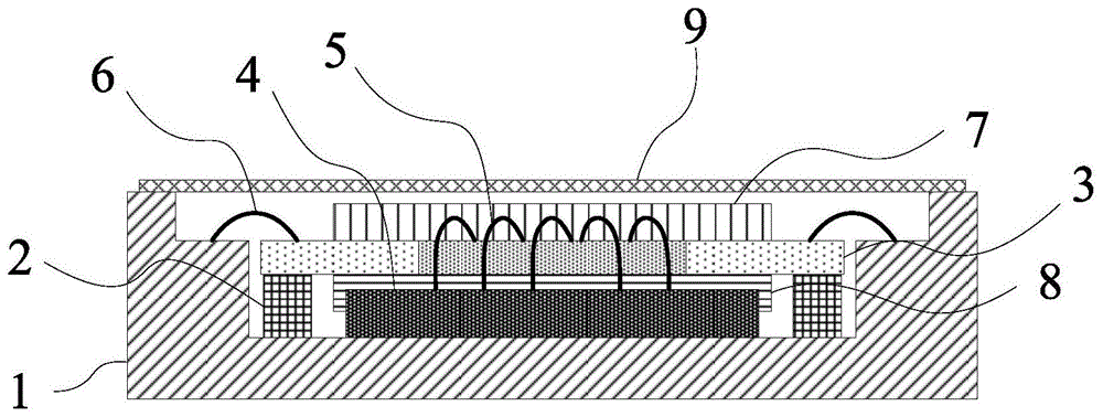
图1为MEMS传感器混合集成封装结构剖面图;Figure 1 is a cross-sectional view of the MEMS sensor hybrid integrated package structure;
图2为MEMS传感器图混合集成封装结构俯视图;Figure 2 is a top view of the hybrid integrated package structure of the MEMS sensor;
图3为MEMS传感器混合集成封装结构剖面图二;Fig. 3 is the second cross-sectional view of the MEMS sensor hybrid integrated package structure;
图4为MEMS传感器电路板外观俯视图;Figure 4 is a top view of the appearance of the MEMS sensor circuit board;
图5为MEMS传感器敏感结构粘接示意图;Fig. 5 is a schematic diagram of MEMS sensor sensitive structure bonding;
图6为MEMS传感器电路板粘接示意图;Fig. 6 is a schematic diagram of MEMS sensor circuit board bonding;
图7~9为三种不同MEMS传感器支撑电容器件粘接方式示意图。7 to 9 are schematic diagrams of three different bonding methods for supporting capacitors of MEMS sensors.
具体实施方式Detailed ways
下面结合实施例以及附图对本发明加以详细说明,所述的实施例仅旨在便于对本发明的理解,并不对其起任何限定作用。The present invention will be described in detail below in conjunction with the embodiments and accompanying drawings. The described embodiments are only intended to facilitate the understanding of the present invention and do not limit it in any way.
MEMS传感器包含MEMS敏感结构4和相应的处理电路。参照图1至图9,一种MEMS传感器混合集成封装结构,用于封装MEMS传感器,包括:陶瓷管壳1、支撑电容2、PCB电路基板3、PCB电路上层电路模块7、PCB电路下层电路模块8、金属盖板9;A MEMS sensor comprises a MEMS
陶瓷管壳1采用LCC封装,内腔在台阶面11的周向设置多个陶瓷管壳金属焊盘111,内腔底面设置有金属化结构;MEMS敏感结构4设置在陶瓷管壳1内腔底面上;PCB电路基板3通过支撑电容2设置在陶瓷管壳1内腔底面上且位于MEMS敏感结构4上方;PCB电路基板3边缘设置PCB电路基板金属焊盘b32和PCB电路基板金属焊盘a31;MEMS敏感结构金属焊盘41与PCB电路基板金属焊盘b32通过MEMS敏感结构键合金属导线5连接;PCB电路基板金属焊盘a31与陶瓷管壳金属焊盘111通过PCB电路基板键合金属导线6连接,通过陶瓷管壳1形成与外部的电学通路;PCB基板3的上下两面分别安装PCB电路上层电路模块7、PCB电路下层电路模块8,PCB电路下层电路模块8与MEMS敏感结构4在水平方向上错开;金属盖板9与所述陶瓷管壳1侧壁连接,形成密封结构。The
金属盖板9由可伐合金制成。所述PCB电路基板3的侧边上开有不少于一处缺口或开槽,用于通过键合用金属导线。所述支撑电容2通过焊接或导电胶粘的方式与PCB电路基板3相连,并通过导电或绝缘胶粘的方式,采用平面贴装或直立贴装的方式,将支撑电容2的不同电极粘接在陶瓷管壳1内腔底面上。The
图7至图9给出了支撑电容2的三种焊接方式,其一为将电容两个电极均焊接或粘接在PCB基板3上,然后分别使用绝缘粘合剂21和导电粘合剂22两种粘合剂粘接不同的电极,从而使电容一端与陶瓷管壳1内腔金属底面形成电气接触,并通过金属底面与其他支撑电容相连;其二为立式焊接或粘接,电容仅有一个电极与PCB基板3焊接或粘接,另一电极通过导电粘合剂22与金属底面相连,此种方式可以使PCB基板3距离底面更高,形成更大的空间容纳不同厚度的MEMS敏感结构4;其三为在方法一条件下,只使用绝缘粘合剂21粘接支撑电容2,电容电极与底面金属之间没有电气连接。所述前两种方法更适用于支撑电容作为滤波电容时使用,此时可将金属底面接地,利于信号屏蔽,第三种方法电容作用不限,但可能需要更复杂的PCB电路设计。Figures 7 to 9 show three welding methods for the supporting
一种MEMS传感器混合集成封装方法,包括以下步骤:A MEMS sensor hybrid integrated packaging method, comprising the following steps:
第一步:根据MEMS传感器选择相应尺寸的陶瓷管壳1;Step 1: Select the
第二步:将MEMS敏感结构4固定在陶瓷管壳1内腔底面;Step 2: Fix the MEMS
第三步:在带有缺口或开槽的PCB电路基板3上焊接PCB电路上层电路模块7、PCB电路下层电路模块8,在PCB电路基板3边缘设置支撑电容2,通过胶粘的方式架设在MEMS敏感结构4上;Step 3: Solder the PCB circuit upper
第四步:MEMS敏感结构键合金属导线5通过PCB电路基板3的缺口或开槽,使用MEMS敏感结构键合金属导线5连接MEMS敏感结构金属焊盘41与PCB电路基板金属焊盘b32,使用PCB电路基板键合金属导线6连接PCB电路基板金属焊盘a31与陶瓷管壳金属焊盘111;The fourth step: the MEMS sensitive structure bonding
第五步:使用平行封焊,将金属盖板9与陶瓷管壳1侧壁连接。Step 5: Connect the
实施例:Example:
所述封装结构包括:The packaging structure includes:
标准陶瓷管壳1,采用LCC封装形式,内腔深度2.4mm,在其内腔台阶面11上设置多个金属焊盘111;所述台阶层11的金属焊盘111与PCB电路基板3的金属焊盘31连接;The standard
所述MEMS敏感结构4,厚度约为0.6mm,通过低应力粘合剂在陶瓷管壳1的底部,对应PCB电路基板3通过支撑电容2粘接在其上,PCB电路基板3和敏感结构4之间无直接接触。The MEMS
本实施例中PCB电路基板3采用U型结构,4层结构,厚度为0.5mm,在矩形的PCB电路基板3的一侧开槽,形成的缺口作为引线键合通道。PCB电路基板3上设置两组金属焊盘,其中;其中一组PCB电路基板金属焊盘b32位于开槽一侧边缘,用于通过MEMS敏感结构键合金属导线5与MEMS敏感结构金属焊盘41连接;一组PCB电路基板金属焊盘a 31位于基板边缘,用于通过PCB电路基板键合金属导线6与陶瓷管壳内腔台阶面11上的金属焊盘111连接,通过陶瓷管壳1形成与外部的电学通路。同时在PCB基板3的上下两面,分别焊接所需的PCB电路上层电路模块7、PCB电路下层电路模块8,由于腔体高度限制,PCB电路下层电路模块8与MEMS敏感结构4在水平方向上错开,两种电路模块厚度均为0.4mm。In this embodiment, the
图5和图6简要说明了本实施例中传感器的封装流程:Figure 5 and Figure 6 briefly illustrate the packaging process of the sensor in this embodiment:
首先在陶瓷管壳1的底面上部,使用低应力粘合剂将MEMS敏感结构4粘接在管壳内,金属焊盘41一侧朝上,与PCB基板缺口方向一致;First, on the bottom surface of the
然后在支撑电容2的电极对应位置分别用绝缘粘合剂21和导电粘合剂22涂覆,将完成器件贴装的PCB电路基板3粘接在陶瓷管壳1上,并通过陶瓷管壳1内腔底面的金属层,形成部分支撑电容之间的电气连接。所用支撑电容2封装为0603,支撑高度为1mm,接下来,分别使用金属引线5和6,完成MEMS敏感结构4和陶瓷管壳1与PCB电路基板之间的电气连接。最后,通过平行封焊,将金属盖板9连接在陶瓷管壳1的侧壁上,形成密闭封装。Then, the corresponding positions of the electrodes of the
本发明未详细说明的部分属于本领域技术人员公知技术。Parts not described in detail in the present invention belong to the well-known technology of those skilled in the art.
Claims (7)
Priority Applications (1)
| Application Number | Priority Date | Filing Date | Title |
|---|---|---|---|
| CN201911284371.6A CN111115552B (en) | 2019-12-13 | 2019-12-13 | A MEMS sensor hybrid integrated packaging structure and packaging method |
Applications Claiming Priority (1)
| Application Number | Priority Date | Filing Date | Title |
|---|---|---|---|
| CN201911284371.6A CN111115552B (en) | 2019-12-13 | 2019-12-13 | A MEMS sensor hybrid integrated packaging structure and packaging method |
Publications (2)
| Publication Number | Publication Date |
|---|---|
| CN111115552A CN111115552A (en) | 2020-05-08 |
| CN111115552B true CN111115552B (en) | 2023-04-14 |
Family
ID=70498780
Family Applications (1)
| Application Number | Title | Priority Date | Filing Date |
|---|---|---|---|
| CN201911284371.6A Active CN111115552B (en) | 2019-12-13 | 2019-12-13 | A MEMS sensor hybrid integrated packaging structure and packaging method |
Country Status (1)
| Country | Link |
|---|---|
| CN (1) | CN111115552B (en) |
Families Citing this family (5)
| Publication number | Priority date | Publication date | Assignee | Title |
|---|---|---|---|---|
| CN114080104B (en) * | 2020-08-19 | 2022-09-27 | 荣耀终端有限公司 | Circuit board assembly and electronic equipment |
| CN113053867B (en) * | 2021-03-09 | 2022-10-18 | 歌尔微电子股份有限公司 | Encapsulation module and electronic equipment |
| CN113406648B (en) * | 2021-06-15 | 2024-05-07 | 江苏英特神斯科技有限公司 | PMUT-based image sonar receiving array and manufacturing method thereof |
| CN115092877A (en) * | 2022-06-09 | 2022-09-23 | 南京理工大学 | Low-stress packaging structure and method for MEMS (micro-electromechanical systems) inertial device based on kovar alloy |
| CN117285000A (en) * | 2023-10-09 | 2023-12-26 | 广州导远电子科技有限公司 | MEMS device fixed knot constructs and electronic equipment |
Citations (8)
| Publication number | Priority date | Publication date | Assignee | Title |
|---|---|---|---|---|
| US6249049B1 (en) * | 1998-06-12 | 2001-06-19 | Nec Corporation | Ceramic package type electronic part which is high in connection strength to electrode |
| CN1708205A (en) * | 2004-06-10 | 2005-12-14 | 国际商业机器公司 | Method and element for realizing resonance oscillation attenuation with electromagnetic compatible shielding |
| CH703289A2 (en) * | 2010-06-11 | 2011-12-15 | Swatch Group Res & Dev Ltd | Encapsulating device for quartz tuning-fork resonator in e.g. electronic watch, has sealing unit comprising alloy formed by nickel with material having less melting point to permit interdiffusion of material with nickel at liquid state |
| US9162869B1 (en) * | 2014-07-31 | 2015-10-20 | Merry Electronics (Shenzhen) Co., Ltd. | MEMS microphone package structure having non-planar substrate and method of manufacturing same |
| CN105008867A (en) * | 2013-02-21 | 2015-10-28 | 埃普科斯股份有限公司 | Sensor system comprising a ceramic housing |
| CN205472637U (en) * | 2016-04-07 | 2016-08-17 | 中国电子科技集团公司第十三研究所 | Micro -electro -mechanical system package substrate |
| CN205873893U (en) * | 2015-09-30 | 2017-01-11 | 意法半导体股份有限公司 | Semi conducting material's air locking |
| CN209572224U (en) * | 2018-11-29 | 2019-11-01 | 湖州品创孵化器有限公司 | A kind of crystal resonator convenient for bending pins and fixation |
Family Cites Families (4)
| Publication number | Priority date | Publication date | Assignee | Title |
|---|---|---|---|---|
| US9794661B2 (en) * | 2015-08-07 | 2017-10-17 | Knowles Electronics, Llc | Ingress protection for reducing particle infiltration into acoustic chamber of a MEMS microphone package |
| US10291236B2 (en) * | 2016-03-15 | 2019-05-14 | Txc Corporation | Oven controlled crystal oscillator consisting of heater-embedded ceramic package |
| US20170283247A1 (en) * | 2016-04-04 | 2017-10-05 | Infineon Technologies Ag | Semiconductor device including a mems die |
| EP3261366B1 (en) * | 2016-06-21 | 2021-09-22 | Sciosense B.V. | Microphone and pressure sensor package and method of producing the microphone and pressure sensor package |
-
2019
- 2019-12-13 CN CN201911284371.6A patent/CN111115552B/en active Active
Patent Citations (8)
| Publication number | Priority date | Publication date | Assignee | Title |
|---|---|---|---|---|
| US6249049B1 (en) * | 1998-06-12 | 2001-06-19 | Nec Corporation | Ceramic package type electronic part which is high in connection strength to electrode |
| CN1708205A (en) * | 2004-06-10 | 2005-12-14 | 国际商业机器公司 | Method and element for realizing resonance oscillation attenuation with electromagnetic compatible shielding |
| CH703289A2 (en) * | 2010-06-11 | 2011-12-15 | Swatch Group Res & Dev Ltd | Encapsulating device for quartz tuning-fork resonator in e.g. electronic watch, has sealing unit comprising alloy formed by nickel with material having less melting point to permit interdiffusion of material with nickel at liquid state |
| CN105008867A (en) * | 2013-02-21 | 2015-10-28 | 埃普科斯股份有限公司 | Sensor system comprising a ceramic housing |
| US9162869B1 (en) * | 2014-07-31 | 2015-10-20 | Merry Electronics (Shenzhen) Co., Ltd. | MEMS microphone package structure having non-planar substrate and method of manufacturing same |
| CN205873893U (en) * | 2015-09-30 | 2017-01-11 | 意法半导体股份有限公司 | Semi conducting material's air locking |
| CN205472637U (en) * | 2016-04-07 | 2016-08-17 | 中国电子科技集团公司第十三研究所 | Micro -electro -mechanical system package substrate |
| CN209572224U (en) * | 2018-11-29 | 2019-11-01 | 湖州品创孵化器有限公司 | A kind of crystal resonator convenient for bending pins and fixation |
Non-Patent Citations (3)
| Title |
|---|
| HU Qi-fang等.Simulation research on structure-related thermal drifts of sensing capacitances of MEMS inertial sensors.《Journal of Chnese Inertial Technology》.2017,第第25卷卷(第第25卷期),第370-377页. * |
| Huan Yuan等.Mems-based semi-packed gas chromatography column with wavy channel configuration.《2016 IEEE International Conference on Manipulation, Manufacturing and Measurement on the Nanoscale (3M-NANO)》.2016,全文. * |
| 王增跃等.硅微加速度计温度特性分析与误差补偿.《传感器与微系统》.2016,第第35卷卷(第第35卷期),第25-28页. * |
Also Published As
| Publication number | Publication date |
|---|---|
| CN111115552A (en) | 2020-05-08 |
Similar Documents
| Publication | Publication Date | Title |
|---|---|---|
| CN111115552B (en) | A MEMS sensor hybrid integrated packaging structure and packaging method | |
| US9337354B2 (en) | Top port MEMS cavity package and method of manufacture thereof | |
| US10531204B2 (en) | Multi-device transducer module, apparatus including the transducer module and method of manufacturing the transducer module | |
| US8837754B2 (en) | Microelectromechanical transducer and corresponding assembly process | |
| JP5763682B2 (en) | Miniaturized electrical device including MEMS and ASIC and method for manufacturing the same | |
| CN102190278B (en) | Semiconductor devices and microphones | |
| EP2393307B1 (en) | Semiconductor device and microphone | |
| CN104891418B (en) | MEMS pressure sensor, MEMS inertial sensor integrated structure | |
| US9986354B2 (en) | Pre-mold for a microphone assembly and method of producing the same | |
| US9428380B2 (en) | Shielded encapsulating structure and manufacturing method thereof | |
| US20070158826A1 (en) | Semiconductor device | |
| US8842859B2 (en) | Packaged microphone with reduced parasitics | |
| US20140210019A1 (en) | Low-cost package for integrated mems sensors | |
| CN104333824A (en) | Surface Mountable Microphone Package, a Microphone Arrangement, a Mobile Phone and a Method for Recording Microphone Signals | |
| US8999757B2 (en) | Top port MEMS cavity package and method of manufacture thereof | |
| CN103583057A (en) | Semiconductor device and microphone | |
| CN107664555A (en) | Media isolation type pressure sensor packaging structure and its method for packing | |
| KR101953089B1 (en) | Lead frame-based chip carrier used in the fabrication of mems transducer packages | |
| KR101060121B1 (en) | Semiconductor package for vertical and horizontal mounting and manufacturing method | |
| CN102020232A (en) | MEMS Acoustic Sensor Package Structure | |
| CN117842926B (en) | Micro differential pressure sensor, packaging structure, test method and electronic equipment | |
| TWM473663U (en) | MEMS microphone device | |
| KR20130028243A (en) | Semicounductor package having micro electronic mechnical system | |
| JP2006129448A (en) | Communication module | |
| CN218320777U (en) | A kind of packaging structure and electronic equipment |
Legal Events
| Date | Code | Title | Description |
|---|---|---|---|
| PB01 | Publication | ||
| PB01 | Publication | ||
| SE01 | Entry into force of request for substantive examination | ||
| SE01 | Entry into force of request for substantive examination | ||
| GR01 | Patent grant | ||
| GR01 | Patent grant |