Phase compensation device and method of Vienna rectifier under low carrier ratio
Technical Field
The invention belongs to the technical field of power electronic conversion, and particularly relates to a phase compensation device and method of a Vienna rectifier under a low carrier ratio.
Background
The Vienna rectifier is a three-level topology, and has the advantages of low voltage stress borne by power switches, small number of power switches, high power density, low input current harmonic content and good adaptability to various PFC control methods, so that the Vienna rectifier is widely applied to the research of power factor correction technology. Meanwhile, in recent years, a lot of documents deeply research is carried out on a three-phase PFC rectifier based on single-cycle control, a controller for single-cycle control generally does not need a multiplier, only simple integration and addition and subtraction operation are carried out on input current, and the input current is directly compared with a reference signal to realize a switching element control waveform with constant modulation frequencyThe method has the advantages of strong stick property and easy realization, and is often used as a main control algorithm of a three-phase PFC rectifier. The traditional single-period control can realize the same phase of input current and input voltage under the condition of input balance and high switching frequency, but under the condition of input unbalance and low switching frequency, because the carrier ratio is low, a Vienna rectifier cannot be equivalent to a DC/DC converter in each switching period, the voltage drop of a filter inductor is increased, and further the input impedance Z (R) at the alternating current side of the rectifier is causedeThe + j ω L is not purely resistive, so that the input current and the input voltage generate phase shift, and the target of unit power factor control cannot be achieved.
The unbalance of three-phase input alternating-current voltage is a special phenomenon in a rectifier power supply system, and can affect the normal operation of the rectifier power supply system, for example, the problems of output direct-current voltage low-frequency pulsation, input power low-frequency pulsation, input current distortion and the like can be caused. For the problems of unbalanced three-phase input ac voltage and phase compensation, document 1(Jin Aijuan, Li Hangtian, Li sharp, and improved one-cycle controlled three-phase PFC receiver under balanced control [ J ]. Transactions of Chinese electronic technical Society,2006,21(7): 115-. The low switching frequency can effectively reduce the switching loss and improve the system efficiency. When the traditional single-period control Vienna rectifier has a low carrier ratio, the input impedance of the alternating current side of the traditional single-period control Vienna rectifier is not pure resistance, so that the power factor of the rectifier is influenced. For the phase compensation problem caused by the low carrier ratio, document 2 (mao peng, xiu jun, francisco, etc.. single-cycle control PFC converter current phase lag and compensation thereof [ J ]. the report of electrotechnical science, 2010, 25 (12): 111- & 118.) performs phase compensation by solving the amplitude phase condition that the modulation wave should satisfy when the low carrier ratio is solved under the rated power condition, but the method does not consider the analysis imbalance condition under the balanced condition.
Disclosure of Invention
The invention aims to provide a phase compensation device and a phase compensation method of a Vienna rectifier under low carrier ratio, which can realize zero phase difference of input voltage and current of each phase under the conditions of unbalanced input and low switching frequency, realize unit power factor operation, reduce the total harmonic distortion rate of alternating current side current, have simple and reliable operation and accurate control.
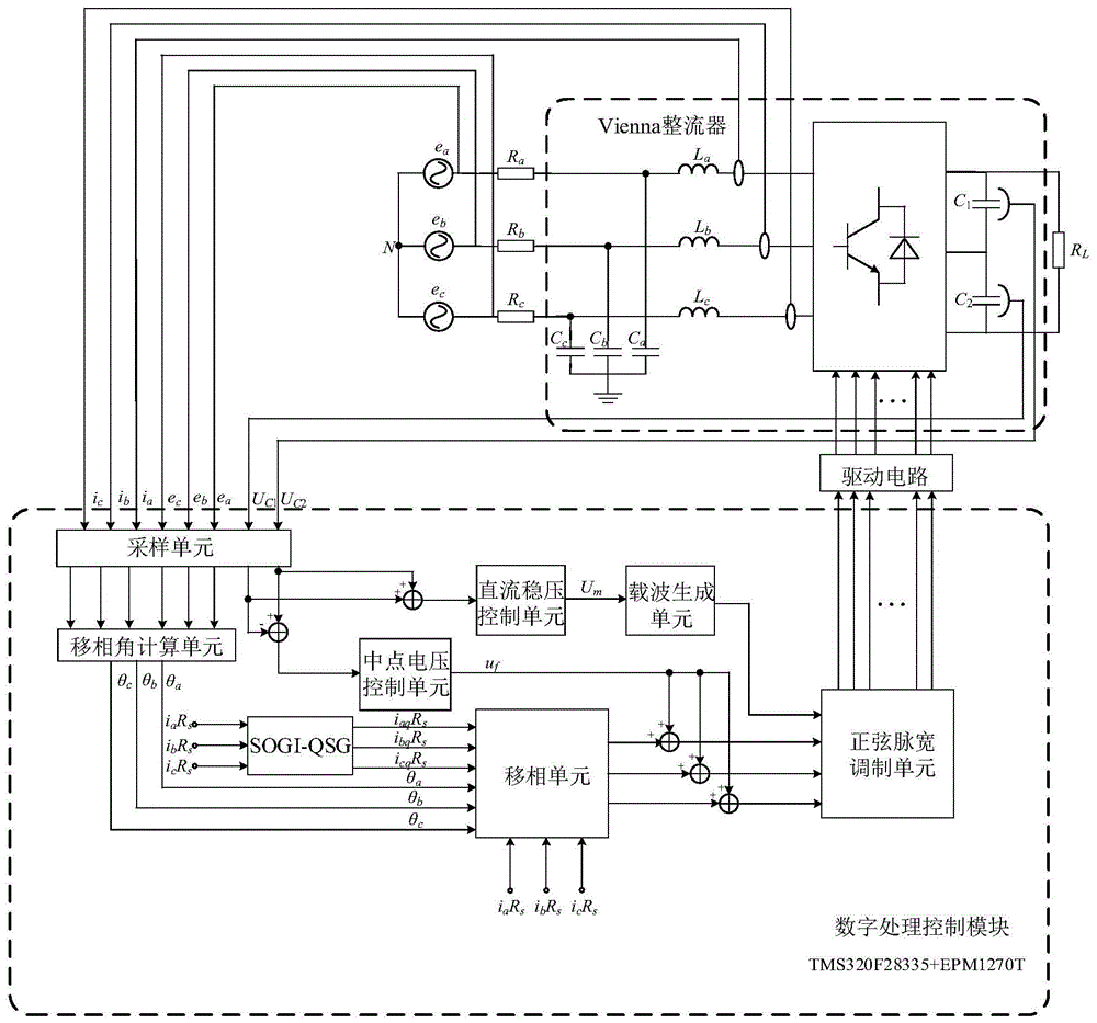
The technical solution for realizing the purpose of the invention is as follows: a phase compensation device of a Vienna rectifier under a low carrier ratio comprises the Vienna rectifier, a digital processing control module and a driving circuit, wherein the digital processing control module comprises a sampling unit, a phase shift angle calculation unit, an orthogonal signal generator unit of a second-order generalized integrator, a phase shift unit, a direct current voltage stabilization control unit, a midpoint voltage control unit, a carrier generation unit and a sine pulse width modulation unit;
the sampling unit is used for respectively acquiring upper and lower capacitor voltage signals on the direct current side of the Vienna rectifier, three-phase voltage signals on the alternating current side of the Vienna rectifier and three-phase current signals on the alternating current side of the Vienna rectifier, and respectively sending the three-phase voltage signals to the phase shift angle calculation unit, the orthogonal signal generator unit of the second-order generalized integrator, the midpoint voltage control unit and the direct current voltage stabilization control unit; the phase shift angle calculation unit calculates and obtains a modulation wave phase shift angle meeting the phase compensation requirement according to the three-phase voltage signals and the current signals on the alternating current side obtained by sampling; the quadrature signal generator unit of the second-order generalized integrator lags the three-phase current signals obtained by sampling by 90 degrees, and sends the signals, the three-phase current signals on the alternating current side and the output signals of the phase shift angle calculation unit to the phase shift unit to obtain three-phase modulation wave signals after phase shifting; the midpoint voltage control unit obtains an output signal of the midpoint voltage control unit according to the sampled upper and lower capacitor voltage signals on the direct current side, and adds the signal and the output signal of the phase shift unit respectively to obtain a modulation signal; the direct current voltage stabilization control unit obtains the amplitude of a carrier signal according to the sampled upper and lower capacitor voltages on the direct current side, and then sends the amplitude to the carrier generation unit to obtain a triangular carrier signal; and the modulation signal and the triangular carrier signal are sent to a sinusoidal pulse width modulation unit, and the output end of the sinusoidal pulse width modulation unit is connected to each switching tube of each phase of bridge arm in the Vienna rectifier through a driving circuit.
Further, the digital processing control module adopts TMS320F28335 and EPM1270T chips.
A phase compensation method of a Vienna rectifier under a low carrier ratio comprises the following steps:
step 1, a sampling unit samples three-phase voltage e at an alternating current sidea、eb、ecAlternating side three-phase current ia、ib、icCapacitor voltage U on the DC sideC1Lower capacitor voltage U on the DC sideC2;
Step 2, sampling three-phase voltage ea、eb、ecThree-phase current ia、ib、icSending the phase shift angle to a phase shift angle calculation unit, and calculating to obtain a phase deviation angle theta of the modulated wave meeting the phase compensation requirementa、θb、θc;
Step 3, detecting three-phase voltage e at alternating current sidea、eb、ecZero-crossing point of (d), and ea、eb、ecThe amplitude of (d);
step 4, according to the three-phase voltage e of the alternating current sidea、eb、ecZero crossing point of (d) and (e)a、eb、ecJudging whether the power grid changes in the operation process of the system;
step 5, sampling three-phase current ia、ib、icAre respectively multiplied by sampling coefficients RsTo obtain iaRs、ibRs、icRsSending the signal to an orthogonal signal generator unit of a second-order generalized integrator to obtain an orthogonal signal iaqRs、ibqRs、icqRs;
Step 6, calculating the phase deviation angle theta obtained in the step 2a、θb、θcSampling the resulting iaRs、ibRs、icRsAnd the step of5, sending the obtained orthogonal signal to a phase shifting unit, and calculating to obtain a modulated wave signal after phase shifting;
step 7, the phase-shifted modulation wave signal m obtained in the step 6 is subjected to phase shiftinga、mb、mcAnd the output u of the midpoint voltage control unitfAdding to obtain final modulated wave signal ma+uf、mb+uf、mc+uf;
Step 8, adding the sampled upper and lower capacitor voltages, sending the added voltages to a direct current voltage stabilization control unit to obtain a triangular carrier amplitude, and then obtaining a triangular carrier signal through a carrier generation unit;
and 9, connecting the three-phase modulation signal obtained in the step 7 with the triangular carrier signal obtained in the step 8 to generate a pulse width modulation signal, and controlling the switch tube of the Vienna rectifier to work through a driving circuit.
Further, the calculation in step 2 obtains a phase deviation angle θ of the modulated wave meeting the phase compensation requirementa、θb、θcThe formula is as follows:
where ω is the grid voltage fundamental angular velocity, L is the filter inductance value, I
a、I
b、I
cRespectively the input current amplitude, E
ano、E
bno、E
cnoRespectively are the non-zero sequence component amplitude values of the power grid,
the phase difference between each phase voltage and the corresponding non-zero sequence component is respectively.
Further, the step 4 is based on the three-phase voltage e of the AC sidea、eb、ecZero crossing point of (d) and (e)a、eb、ecThe amplitude value of the power grid is judged to be changed or not in the running process of the system, and the method specifically comprises the following steps:
step 4.1, sampling three-phase power grid voltage at the alternating current side, and calculating a modulation wave phase deviation angle meeting the phase compensation requirement;
step 4.2, setting the maximum allowable error angle of each phase
Measuring the zero crossing point of each phase voltage in the first power frequency period
Then, each power frequency period detects the zero crossing point of each phase voltage, and the zero crossing point of the kth period is set as
Will be compared with the zero crossing point of the previous cycle
Make a comparison if
If x is a, b, c, the phase shift angle θ of the modulated wave meeting the phase compensation requirement needs to be recalculated
a、θ
b、θ
cSkipping to step 4.1; if it is
The phase of the grid voltage does not change between the kth period and the kth-1 period, and the step 4.3 is carried out;
step 4.3, setting the maximum allowable error amplitude E of each phaseerroMeasuring the amplitude of the grid voltage in the kth period, comparing the amplitude with the amplitude of the kth-1 period, and determining if the amplitude is Exk-Ex(k-1)|<EerroIf x is a, b and c, the voltage of the power grid is not changed, and the next power frequency period is started; if | Exk-Ex(k-1)|>EerroIf the grid voltage changes, the phase deviation angle theta of the modulated wave meeting the phase compensation requirement is recalculateda、θb、θcAnd skipping to step 4.1.
Further, in step 6, the calculation obtains a modulated wave signal after phase shifting, and the formula is as follows:
in the formula, RsFor sampling the coefficient of the AC side current, ia、ib、icIs a three-phase current of the AC side, iaq、ibq、icqIs a signal orthogonal to the AC side current, θa、θb、θcFor each phase shift phase angle.
Further, the three-phase modulation signal obtained in step 7 is connected with the triangular carrier signal obtained in step 8 in step 9 to generate a pulse width modulation signal, and the Vienna rectifier switching tube is controlled to work through the driving circuit, which specifically includes the following steps:
the core control equation for improving the single-cycle control is as follows:
in the formula of UmFor the output signal of the DC regulation control unit, dA、dB、dCRespectively the conduction duty ratio, R, of each phase of switching tubesFor sampling the coefficient of the AC side current, ia、ib、icIs a three-phase current of the AC side, iaq、ibq、icqIs a signal orthogonal to the AC side current, θa、θb、θcFor each phase shift phase angle ufThe output signal is the midpoint voltage control unit.
Compared with the prior art, the invention has the remarkable advantages that: (1) the phase shift problem between the alternating-current side voltage and the current of the Vienna rectifier under the conditions of unbalanced input and low carrier ratio is effectively solved, and the alternating-current side of the Vienna rectifier realizes unit power factor operation; (2) the total harmonic distortion rate of the alternating current side current is reduced by introducing the midpoint voltage control unit, and the waveform quality is improved; (3) the method is suitable for the conditions of unbalanced input and low switching frequency, and has the advantages of simple and reliable operation, low hardware cost, accurate control and wide application range.
Drawings
Fig. 1 is a schematic structural diagram of a phase compensation device of a Vienna rectifier under a low carrier ratio in the invention.
Fig. 2 is a schematic diagram of a quadrature signal generator unit of the second-order generalized integrator of the present invention.
Fig. 3 is a topology of the Vienna rectifier of the present invention.
Fig. 4 is a single-phase equivalent circuit diagram of the Vienna rectifier of the present invention.
Fig. 5 is a relation diagram of each vector in the single-phase equivalent circuit of the Vienna rectifier in the invention.
Fig. 6 is a flow chart of the calculation of the phase shift angle in the present invention.
Fig. 7 is a waveform diagram of an input unbalanced voltage in an embodiment of the present invention.
FIG. 8 is a comparison graph of the magnitude of the phase difference between the phase of the A-phase voltage and the phase of the A-phase current on the front and rear AC sides using the method of the present invention in an embodiment of the present invention, wherein (a) is a simulation waveform using the conventional single-cycle control, and (b) is a simulation waveform using the control method of the present invention.
Fig. 9 is a comparison graph of the harmonic distribution of the ac side current before and after the method of the present invention is used in the example of the present invention, where (a) is the harmonic distribution of the ac side current before the control method of the present invention is used, and (b) is the harmonic distribution of the ac side current after the control method of the present invention is used.
Detailed Description
The invention is described in further detail below with reference to the figures and specific examples.
With reference to fig. 1, 2, and 3, the phase compensation apparatus for a Vienna rectifier with a low carrier ratio of the present invention includes a Vienna rectifier, a digital processing control module and a driving circuit, wherein the digital processing control module includes a sampling unit, a phase shift angle calculation unit, a Quadrature Signal Generator unit (SOGI-QSG) of a Second-Order Generalized Integrator, a phase shift unit, a dc voltage stabilization control unit, a midpoint voltage control unit, a carrier generation unit, and a sine pulse width modulation unit;
the quadrature signal generator unit (SOGI-QSG) of the second order generalized integrator is shown in fig. 2, where V is the input signal, V 'is the signal in phase with V, qV' is the signal lagging by V90 °, and ω is the fundamental angular velocity of the input signal;
the sampling unit is used for respectively acquiring upper and lower capacitor voltage signals on the direct current side of the Vienna rectifier, three-phase voltage signals on the alternating current side of the Vienna rectifier and three-phase current signals on the alternating current side of the Vienna rectifier, and respectively sending the three-phase voltage signals to the phase shift angle calculation unit, the orthogonal signal generator unit of the second-order generalized integrator, the midpoint voltage control unit and the direct current voltage stabilization control unit; the phase shift angle calculation unit calculates and obtains a modulation wave phase shift angle meeting the phase compensation requirement according to the three-phase voltage signals and the current signals on the alternating current side obtained by sampling; the quadrature signal generator unit of the second-order generalized integrator lags the three-phase current signals obtained by sampling by 90 degrees, and sends the signals, the three-phase current signals on the alternating current side and the output signals of the phase shift angle calculation unit to the phase shift unit to obtain three-phase modulation wave signals after phase shifting; the midpoint voltage control unit obtains an output signal of the midpoint voltage control unit according to the sampled upper and lower capacitor voltage signals on the direct current side, and adds the signal and the output signal of the phase shift unit respectively to obtain a modulation signal; the direct current voltage stabilization control unit obtains the amplitude of a carrier signal according to the sampled upper and lower capacitor voltages on the direct current side, and then sends the amplitude to the carrier generation unit to obtain a triangular carrier signal; and the modulation signal and the triangular carrier signal are sent to a sinusoidal pulse width modulation unit, and the output end of the sinusoidal pulse width modulation unit is connected to each switching tube of each phase of bridge arm in the Vienna rectifier through a driving circuit.
As a specific example, the digital processing control module adopts TMS320F28335 and EPM1270T chips.
A phase compensation method of a Vienna rectifier under a low carrier ratio comprises the following steps:
step 1, samplingUnit sampling AC side three-phase voltage ea、eb、ecAlternating side three-phase current ia、ib、icCapacitor voltage U on the DC sideC1Lower capacitor voltage U on the DC sideC2;
Step 2, sampling the three-phase voltage e in each switching perioda、eb、ecThree-phase current ia、ib、icCalculating to obtain the phase deviation angle theta of the modulated wave meeting the phase compensation requirementa、θb、θcThe method comprises the following steps:
according to the Vienna rectifier single-phase equivalent circuit shown in fig. 4 and the vector relationship diagram in the single-phase equivalent circuit shown in fig. 5, the following relationship can be obtained:
wherein g is A, B, C, I
gFor each phase current amplitude, L is the filter inductance value, E
gnoFor each phase non-zero sequence component magnitude,
the difference between the voltage phase and the non-zero sequence component phase of each phase of the network, E
gOThe amplitude of the fundamental wave of the bridge arm voltage of each phase is obtained.
Further obtaining the phase deviation angle theta of the modulated wave meeting the phase compensation requirementa、θb、θcComprises the following steps:
where ω is the grid voltage fundamental angular velocity, L is the filter inductance value, I
a、I
b、I
cRespectively the input current amplitude, E
ano、E
bno、E
cnoRespectively are the non-zero sequence component amplitude values of the power grid,
the phase difference between each phase voltage and the corresponding non-zero sequence component is respectively.
Step 3, detecting three-phase voltage e at alternating current sidea、eb、ecZero-crossing point of (d), and ea、eb、ecThe amplitude of (d);
step 4, according to the three-phase voltage e of the alternating current sidea、eb、ecZero crossing point of (d) and (e)a、eb、ecThe amplitude of the voltage, whether the power grid changes during the operation of the system, in combination with fig. 6, is as follows:
step 4.1, sampling voltage and current of a three-phase power grid at the alternating current side, and calculating a phase deviation angle of a modulation wave meeting the phase compensation requirement;
step 4.2, setting the maximum allowable error angle of each phase
Measuring the zero crossing point of each phase voltage in the first power frequency period
Then, each power frequency period detects the zero crossing point of each phase voltage, and the zero crossing point of the kth period is set as
Will be compared with the zero crossing point of the previous cycle
Make a comparison if
Wherein x is a, b and c, and the phase deviation angle theta of the modulated wave meeting the phase compensation requirement needs to be recalculated
a、θ
b、θ
cSkipping to step 4.1; if it is
The phase of the grid voltage does not change between the kth period and the kth-1 period, and the step 4.3 is carried out;
step 4.3, setting the maximum allowable error amplitude E of each phaseerroMeasuring the amplitude of the grid voltage in the kth period, comparing the amplitude with the amplitude of the kth-1 period, and determining if the amplitude is Exk-Ex(k-1)|<Eerro(wherein x is a, b and c), the voltage of the power grid is not changed, and the next power frequency period is started; if | Exk-Ex(k-1)|>EerroIf the grid voltage changes, the phase deviation angle theta of the modulated wave meeting the phase compensation requirement needs to be recalculateda、θb、θcAnd skipping to step 4.1.
Step 5, sampling three-phase current ia、ib、icAre respectively multiplied by sampling coefficients RsTo obtain iaRs、ibRs、icRsSending the signal to an orthogonal signal generator unit of a second-order generalized integrator to obtain an orthogonal signal iaqRs、ibqRs、icqRs;
Step 6, calculating the phase deviation angle theta obtained in the step 4a、θb、θcSampling the resulting iaRs、ibRs、icRsAnd the orthogonal signal obtained in the step 5 is sent to a phase shifting unit, and a modulated wave signal after phase shifting is obtained through calculation, wherein the formula is as follows:
in the formula, RsFor sampling the coefficient of the AC side current, ia、ib、icIs a three-phase current of the AC side, iaq、ibq、icqIs a signal orthogonal to the AC side current, θa、θb、θcFor each phase shift phase angle.
Step 7, the phase-shifted modulation wave signal m obtained in the step 6 is subjected to phase shiftinga、mb、mcAnd the output u of the midpoint voltage control unitfAdding to obtain final modulated wave signal ma+uf、mb+uf、mc+uf;
Step 8, adding the sampled upper and lower capacitor voltages, sending the added voltages to a direct current voltage stabilization control unit to obtain a triangular carrier amplitude, and then obtaining a triangular carrier signal through a carrier generation unit;
and 9, connecting the three-phase modulation signal obtained in the step 7 with the triangular carrier signal obtained in the step 8 to generate a pulse width modulation signal, and controlling a switch tube of the Vienna rectifier to work through a driving circuit, wherein the method specifically comprises the following steps:
the core control equation for improving the one-cycle control at this time is as follows:
in the formula of UmFor the output signal of the DC regulation control unit, dA、dB、dCRespectively the conduction duty ratio u of each phase of switching tubefThe output signal is the midpoint voltage control unit.
The modulation rule of the Vienna rectifier is: taking phase A as an example, in the positive half cycle of the modulated wave, when the carrier wave is larger than the modulated wave, let Sa1、Sa2Conducting, the voltage of the A-phase bridge arm is 0, and when the carrier wave is less than the modulation wave, making Sa1、Sa2Turn off, the A phase bridge arm voltage is V DC2; in the negative half cycle of the modulated wave, when the carrier wave is smaller than the modulated wave, let Sa1、Sa2Conducting, the voltage of the A-phase bridge arm is 0, and when the carrier wave is greater than the modulation wave, making Sa1、Sa2Turn off, the A phase bridge arm voltage is-VDC/2. B. The modulation strategy of the C two phases is the same as that of the A phase.
Wherein VDCThe voltage is the voltage of a direct current bus at the output side of the Vienna rectifier.
Example 1
In this embodiment, a three-phase Vienna rectifying circuit is built by using a Simulink tool in MATLAB, and the input voltage is rectified by the three-phase Vienna rectifying circuit to obtain direct current. The electrical parameter settings during the simulation are as in table 1:
TABLE 1
Table 1 shows Simulink simulation parameters, in order to unbalance the input voltage, the amplitude of the C-phase of the input voltage is reduced by 20%, and the phase of the C-phase is advanced by 60 °, fig. 7 is a voltage waveform diagram of the input unbalance, the amplitude of the C-phase of the input voltage is reduced by 20%, and the phase of the C-phase is advanced by 60 °.
Fig. 8 is a schematic diagram of the phase shift angle between the voltage and the current on the ac side before and after the control method of the present invention is used under the above electrical parameters, where fig. 8(a) is a waveform diagram under the conventional single-cycle control, and the phase shift angle is 36 ° in this case, and fig. 8(b) is a waveform diagram of the voltage and the current after the control method of the present invention is used, and the phase shift angle is 11 ° in this case.
Fig. 9(a) and (b) show the total harmonic distortion of the grid-side current before and after the compensation control method of the present invention, respectively, where fig. 9(a) is an ac-side current harmonic distribution diagram (Fundamental (50Hz) ═ 14.2 and THD ═ 3.27%) before the compensation control method of the present invention is used, and fig. 9(b) is an ac-side current harmonic distribution diagram (Fundamental (50Hz) ═ 18.7 and THD ═ 2.95%) after the compensation control method of the present invention is used.
TABLE 2
Table 2 is a table of power factors of each phase under the same simulation conditions with the method of the present invention, and it can be seen from table 2, fig. 8 and fig. 9 that the present invention can effectively solve the problem of phase shift between the voltage and the current of the alternating current side of the Vienna rectifier based on low switching frequency in the unbalanced power grid, and reduce the total harmonic distortion of the current of the alternating current side.