CN110140009B - Microstructured and patterned light guide plates and devices incorporating same - Google Patents
Microstructured and patterned light guide plates and devices incorporating same Download PDFInfo
- Publication number
- CN110140009B CN110140009B CN201780081835.6A CN201780081835A CN110140009B CN 110140009 B CN110140009 B CN 110140009B CN 201780081835 A CN201780081835 A CN 201780081835A CN 110140009 B CN110140009 B CN 110140009B
- Authority
- CN
- China
- Prior art keywords
- light guide
- light
- guide plate
- mol
- major surface
- Prior art date
- Legal status (The legal status is an assumption and is not a legal conclusion. Google has not performed a legal analysis and makes no representation as to the accuracy of the status listed.)
- Active
Links
Images


Classifications
-
- G—PHYSICS
- G02—OPTICS
- G02B—OPTICAL ELEMENTS, SYSTEMS OR APPARATUS
- G02B6/00—Light guides; Structural details of arrangements comprising light guides and other optical elements, e.g. couplings
- G02B6/0001—Light guides; Structural details of arrangements comprising light guides and other optical elements, e.g. couplings specially adapted for lighting devices or systems
- G02B6/0011—Light guides; Structural details of arrangements comprising light guides and other optical elements, e.g. couplings specially adapted for lighting devices or systems the light guides being planar or of plate-like form
- G02B6/0065—Manufacturing aspects; Material aspects
-
- G—PHYSICS
- G02—OPTICS
- G02B—OPTICAL ELEMENTS, SYSTEMS OR APPARATUS
- G02B6/00—Light guides; Structural details of arrangements comprising light guides and other optical elements, e.g. couplings
- G02B6/0001—Light guides; Structural details of arrangements comprising light guides and other optical elements, e.g. couplings specially adapted for lighting devices or systems
- G02B6/0011—Light guides; Structural details of arrangements comprising light guides and other optical elements, e.g. couplings specially adapted for lighting devices or systems the light guides being planar or of plate-like form
- G02B6/0033—Means for improving the coupling-out of light from the light guide
- G02B6/005—Means for improving the coupling-out of light from the light guide provided by one optical element, or plurality thereof, placed on the light output side of the light guide
- G02B6/0051—Diffusing sheet or layer
-
- G—PHYSICS
- G02—OPTICS
- G02B—OPTICAL ELEMENTS, SYSTEMS OR APPARATUS
- G02B6/00—Light guides; Structural details of arrangements comprising light guides and other optical elements, e.g. couplings
- G02B6/0001—Light guides; Structural details of arrangements comprising light guides and other optical elements, e.g. couplings specially adapted for lighting devices or systems
- G02B6/0011—Light guides; Structural details of arrangements comprising light guides and other optical elements, e.g. couplings specially adapted for lighting devices or systems the light guides being planar or of plate-like form
- G02B6/0033—Means for improving the coupling-out of light from the light guide
- G02B6/0035—Means for improving the coupling-out of light from the light guide provided on the surface of the light guide or in the bulk of it
- G02B6/0036—2-D arrangement of prisms, protrusions, indentations or roughened surfaces
-
- G—PHYSICS
- G02—OPTICS
- G02B—OPTICAL ELEMENTS, SYSTEMS OR APPARATUS
- G02B6/00—Light guides; Structural details of arrangements comprising light guides and other optical elements, e.g. couplings
- G02B6/0001—Light guides; Structural details of arrangements comprising light guides and other optical elements, e.g. couplings specially adapted for lighting devices or systems
- G02B6/0011—Light guides; Structural details of arrangements comprising light guides and other optical elements, e.g. couplings specially adapted for lighting devices or systems the light guides being planar or of plate-like form
- G02B6/0033—Means for improving the coupling-out of light from the light guide
- G02B6/0035—Means for improving the coupling-out of light from the light guide provided on the surface of the light guide or in the bulk of it
- G02B6/0038—Linear indentations or grooves, e.g. arc-shaped grooves or meandering grooves, extending over the full length or width of the light guide
-
- G—PHYSICS
- G02—OPTICS
- G02B—OPTICAL ELEMENTS, SYSTEMS OR APPARATUS
- G02B6/00—Light guides; Structural details of arrangements comprising light guides and other optical elements, e.g. couplings
- G02B6/0001—Light guides; Structural details of arrangements comprising light guides and other optical elements, e.g. couplings specially adapted for lighting devices or systems
- G02B6/0011—Light guides; Structural details of arrangements comprising light guides and other optical elements, e.g. couplings specially adapted for lighting devices or systems the light guides being planar or of plate-like form
- G02B6/0033—Means for improving the coupling-out of light from the light guide
- G02B6/005—Means for improving the coupling-out of light from the light guide provided by one optical element, or plurality thereof, placed on the light output side of the light guide
- G02B6/0053—Prismatic sheet or layer; Brightness enhancement element, sheet or layer
Abstract
Disclosed herein is a light guide plate (100, 100', 100 ") comprising: a transparent substrate (110) having an edge surface (150), a first major surface (160) that emits light, and an opposite second major surface (170); and a polymeric film (120) disposed on at least one of the first major surface (160) and the second major surface (170) of the transparent substrate, wherein the polymeric film (120) comprises a plurality of microstructures (130) and/or a plurality of light extraction features. At least one light source (140) may be connected to an edge surface (150) of the transparent substrate (110). Display and lighting devices comprising such light guide plates, and methods of manufacturing such light guide plates are also disclosed.
Description
CROSS-REFERENCE TO RELATED APPLICATIONS
Priority of united states provisional application serial No. 62/440,029 filed 2016, 12, 29, 35u.s.c. § 119 requirements 2016, the contents of which are incorporated herein by reference in their entirety.
Technical Field
The present disclosure relates generally to light guide plates and display or lighting devices incorporating such light guide plates, and more particularly to light guide plates incorporating polymeric films that are patterned with a plurality of microstructures and/or light extraction features.
Background
Liquid Crystal Displays (LCDs) are commonly used in a variety of electronic devices, such as cell phones, laptop computers, electronic boards, televisions, and computer monitors. However, LCDs are limited in brightness, contrast, efficiency, and viewing angle compared to other displays. For example, to compete with other display technologies, conventional LCDs have required higher contrast, color saturation, and brightness, while also balancing power requirements and device size (e.g., thickness).
An LCD may include a backlight unit (BLU) for generating light, which is then converted, filtered, and/or polarized to produce a desired image. The BLU can be illuminated at the edge, e.g., containing light sources connected to the edge of a Light Guide Plate (LGP), or from the back, e.g., containing a two-dimensional array of light sources disposed behind the LCD panel. Direct illumination BLUs may have the advantage of improved dynamic contrast compared to edge-illumination BLUs. For example, a display with a direct-lit BLU can independently adjust the brightness of each LED to optimize the brightness dynamic range of the entire image. This is commonly referred to as local dimming. However, to achieve the desired light uniformity and/or avoid hot spots in the direct illumination BLU, the light source may be positioned a distance from the LGP, thus making the overall display thickness greater than that of the edge illumination BLU. In a conventional edge-lit BLU, the light from each LED may be distributed over a large area of the LGP, such that turning off several LEDs or groups of LEDs may have only a small impact on the dynamic contrast ratio.
Local dimming efficiency of the LGP may be improved by, for example, providing one or more microstructures on the surface of the LGP. For example, a plastic LGP such as a Polymethylmethacrylate (PMMA) or a methyl methacrylate-styrene (MS) LGP can have surface microstructures, e.g., microlenses, fabricated thereon that confine light from each LED to a narrow band. This makes it possible to adjust the source brightness along the edges of the LGP, improving the dynamic contrast of the display. If the LEDs are mounted on two opposite sides of the LGP, the brightness of the paired LEDs can be adjusted to produce a brightness gradient along the illumination band, which can further improve dynamic contrast.
It may also be advantageous to improve the color uniformity and/or intensity of light extracted from an LGP by improving the LGP. For example, at least one surface of the LGP may be modified to include light extraction features to frustrate Total Internal Reflection (TIR) within the LGP. In some cases, the density of light extraction features may increase with increasing distance from the light source. Techniques for modifying the surface of an LGP to form microstructures and/or light extraction features may include, for example, screen printing, ink jet printing, hot embossing (imprinting), and laser embossing. Laser imprinting has certain advantages in patterned pattern control (e.g., using software), reduced processing time, repeatability, and manufacturing flexibility. Hot stamping may also have advantages in improving control over feature shape, repeatability, and large-scale processing capabilities.
Glass LGPs can bring various improvements compared to plastic LGPs, for example in their low optical attenuation, low coefficient of thermal expansion, and high mechanical strength. Accordingly, to overcome various drawbacks associated with plastics, it may be desirable to manufacture LGPs from glass as an alternative material. For example, it may be difficult to manufacture a plastic LGP that is both large and thin enough to meet current consumer demands due to its weak mechanical strength and/or low stiffness. Plastic LGPs may also require a large gap between the light source and the LGP due to their high coefficient of thermal expansion, which may reduce the efficiency of light coupling and/or require a larger bezel for the display. In addition, plastic LGPs may be more prone to moisture absorption and swelling than glass LGPs.
With the above advantages, many display manufacturers are replacing plastic LGPs with glass LGPs, for example, to produce thinner displays. However, it can be difficult to process a glass LGP using the same methods and/or equipment used to process plastic LGPs. For example, hot embossing techniques such as injection molding, extrusion, and/or embossing (embossing) are effective for plastic LGPs, but they may not be suitable for glass LGPs because glass LGPs have higher glass transition temperatures and/or higher viscosities. Furthermore, although it is possible to modify the glass substrate with a laser, the stability of the glass makes the laser embossing process more difficult than for a plastic LGP.
Therefore, it would be advantageous if a glass LGP having improved local dimming efficiency could be provided, such as a glass LGP having a microstructure on at least one surface thereof. Furthermore, it would be advantageous if a glass LGP could be provided that had improved light uniformity, such as a glass LGP having patterned light extraction features on at least one surface thereof. It would also be advantageous if a simple and/or cost effective method could be provided for providing an LGP surface having microstructural and/or light extraction features. It would be further advantageous to provide a backlight that is thin similar to that of an edge-lit BLU, while providing local dimming capabilities similar to those of a back-lit BLU.
SUMMARY
In various embodiments, the present disclosure relates to a light guide plate comprising: a transparent substrate having an edge surface, a first major surface that emits light, and an opposing second major surface; and a polymeric film disposed on the second major surface of the transparent substrate, wherein the polymeric film comprises a plurality of microstructures patterned with a plurality of light extraction features. Also disclosed herein is a light guide plate comprising: a glass substrate having an edge surface, a first major surface that emits light, and an opposing second major surface; and a polymeric film disposed on at least one of the first major surface and the second major surface of the glass substrate, wherein the polymeric film comprises a plurality of light extraction features. Further disclosed herein is a light guide assembly comprising a light guide plate as disclosed herein, the light guide plate being optically connected to at least one light source; and a display device, an electronic device and a lighting device comprising such a light guide plate and assembly.
In some embodiments, the light guide plate may have a color shift Δ y of less than about 0.05. According to various embodiments, the transparent substrate may be a glass substrate, for example comprising a glass composition comprising: 50-90 mol% SiO 20 to 20 mol% Al2O30 to 20 mol% B2O30-20 mol% P2O50 to 25 mol% RxO, wherein x is 1 or 2, R is Li, Na, K, Rb, Cs, Zn, Mg, Ca, Sr, Ba, and combinations thereof. In other embodiments, the transparent substrate may comprise less than about 1ppm of each of Co, Ni, and Cr. The transparent substrate may have a thickness in the range of about 0.1mm to about 3mm, and the polymer film may have a thickness in the range of about 5 μm to about 500 μm.
In certain embodiments, the polymer film may comprise a UV-curable or thermally-curable polymer that may be molded onto the light-emitting surface of the glass substrate. In other embodiments, the polymer film is laminated to the transparent substrate with an intermediate adhesive layer. For example, the polymeric film can comprise a periodic or aperiodic microstructure array comprising prisms, rounded prisms, or lenticular lenses. The aspect ratio of the microstructures can be, for example, in the range of about 0.1 to about 3. According to non-limiting embodiments, the plurality of light extraction features may have a triangular, trapezoidal, or parabolic cross-sectional profile. The light extraction features may have at least one dimension less than about 100 μm.
Also disclosed herein is a method for forming a light guide plate, the method comprising: a layer of polymeric material is applied on a major surface of the transparent substrate and shaped to produce a plurality of microstructures patterned with a plurality of light extraction features. According to various embodiments, the method may include applying a layer of polymeric material on a major surface of the transparent substrate opposite the light emitting surface. In certain embodiments, the layer of polymeric material may be applied by screen printing. Shaping of the polymeric material can be carried out by, for example, microreplication, UV embossing, thermal embossing or hot embossing. The methods disclosed herein may also include one or more steps of forming a forming mold. The step of shaping the polymeric material may comprise applying a shaping mould to the layer of polymeric material.
Also disclosed herein is a method for forming a light guide plate, the method comprising: a layer of polymeric material is applied on at least one major surface of the transparent substrate and the polymeric material is modified to produce a plurality of light extraction features. In non-limiting embodiments, modifying the polymeric material may include thermally embossing and/or laser embossing the polymeric material.
Additional features and advantages of the disclosure will be set forth in the detailed description which follows, and in part will be readily apparent to those skilled in the art from that description or recognized by practicing the methods as described herein, including the detailed description which follows, the claims, as well as the appended drawings.
It is to be understood that both the foregoing general description and the following detailed description describe various embodiments of the disclosure, and are intended to provide an overview or framework for understanding the nature and character of the claims. The accompanying drawings are included to provide a further understanding of the disclosure, and are incorporated in and constitute a part of this specification. The drawings illustrate various embodiments of the disclosure and together with the description serve to explain the principles and operations of the disclosure.
Brief Description of Drawings
A further understanding can be obtained when the following detailed description is read in conjunction with the following drawings.
1A-C illustrate an exemplary LGP having a surface patterned with micro-structures and/or light extraction features in accordance with various embodiments of the present disclosure;
FIG. 2 illustrates a light guide assembly according to certain embodiments of the present disclosure;
FIGS. 3A-D illustrate exemplary microstructure profiles;
FIG. 4 is a graph showing the color shift Δ y of a light guide plate as a function of the ratio of blue/red transmittance;
FIG. 5 is a graphical representation of the transmittance curves of various LGPs;
FIG. 6 is a graphical representation of the refractive index dispersion of glass and polymer materials;
FIG. 7 is a graphical representation of Fresnel reflectivity for glass substrates having different polymer layers;
FIGS. 8A-8D and 9A-9H illustrate methods of forming and patterning microstructured films according to non-limiting embodiments of the present disclosure;
fig. 10 illustrates an exemplary glass-polymer laminate LGP patterned with light extraction features;
11A-C are topographical views of light extraction features formed according to some embodiments of the present disclosure;
12A-C illustrate cross-sectional views of light extraction features formed according to certain embodiments of the present disclosure;
FIG. 13A illustrates an exemplary LGP that includes a microstructured surface and a printing surface;
13B-C illustrate light guide plates including microstructured surfaces patterned with a plurality of light extraction features according to some embodiments of the present disclosure;
14A-E depict the beam widths of various LGPs; and
fig. 15 is a graphical representation of normalized luminous flux as a function of distance from the center of the light source for the various configurations shown in fig. 14A-E.
Detailed Description
Light guide plate
The present disclosure discloses a light guide plate, comprising: a transparent substrate having an edge surface, a first major surface that emits light, and an opposing second major surface; and a polymeric film disposed on the second major surface of the transparent substrate, wherein the polymeric film comprises a plurality of microstructures patterned with a plurality of light extraction features. Also disclosed herein is a light guide plate comprising: a glass substrate having an edge surface, a first major surface that emits light, and an opposing second major surface; and a polymeric film disposed on at least one of the first major surface and the second major surface of the glass substrate, wherein the polymeric film comprises a plurality of light extraction features. Further disclosed herein is a light guide assembly comprising the light guide plate disclosed herein optically connected to at least one light source. Also disclosed herein are various devices, such as display devices, lighting devices, and electronic devices, such as televisions, computers, telephones, flat panels, and other display panels, luminaires, solid state lighting, billboards and other architectural elements, and the like, that include such light guides.
Various embodiments of the present disclosure will be discussed below in conjunction with fig. 1-15, which illustrate exemplary embodiments of light guide plates and methods of making and operating the same. The following general description is intended to provide an overview of the claimed apparatus, and various aspects will be discussed more particularly throughout the disclosure in conjunction with non-limiting, illustrative embodiments, which are interchangeable with one another in the context of this disclosure.
FIGS. 1A-C illustrate exemplary Light Guide Plates (LGPs) 100, 100', 100 "that include a transparent substrate 110 and a polymer film 120. As shown in fig. 1A-B, the polymer film can comprise a plurality of microstructures 130. The polymer film 120 can also be patterned with light extraction features 135, 135', 135", as shown in fig. 1A-C. The polymeric films 120 may be present on one or both major surfaces of the transparent substrate and may be the same or different. In some embodiments, the light extraction pattern shown in FIG. 1A can be generated using the exemplary methods discussed below in connection with FIGS. 8A-D. In some embodiments, the light extraction pattern shown in FIG. 1B can be generated using the exemplary methods discussed below in connection with FIGS. 9A-H. In various embodiments, the light extraction pattern shown in fig. 1C can be produced using, for example, the laser and/or thermal embossing techniques discussed in connection with fig. 10. Of course, the light extraction pattern shown is merely exemplary and can be varied as needed to produce any desired light extraction effect.
As shown in fig. 2, the at least one light source 140 may be optically connected to an edge surface 150 of the transparent substrate 110, e.g., disposed adjacent to the edge 150. As used herein, the term "optically connected" means that the light source is disposed at an edge of the LGP, thereby introducing light into the LGP. The light source may be optically connected to the LGP even if it is not in physical contact with the LGP. Other light sources (not shown) may also be optically connected to other edge surfaces of the LGP, such as adjacent or opposing edge surfaces. Although fig. 2 illustrates an LGP having a microstructured polymer film, it is to be understood that LGPs having any configuration (e.g., as illustrated in fig. 1A-C) and any variation thereof can be connected to the light source 140.
The general direction of light emitted by the light source 140 is indicated in fig. 2 by solid arrows. Light injected into the LGP may propagate along the length L of the LGP using Total Internal Reflection (TIR) until its angle of incidence at the interface is less than the critical angle. Total Internal Reflection (TIR) is a phenomenon: when a first material (e.g., glass, plastic, etc.) has a first refractive index and a second material (e.g., air, etc.) has a second refractive index that is less than the first refractive index, light energy propagating in the first material is totally reflected at an interface with the second material. TIR can be explained by snell's law:
n1sin(θi)=n2sin(θr)
this law describes the refraction of light at the interface between two materials having different refractive indices. According to the snell's law, n1Is the refractive index of the first material, n2Is the refractive index of the second material, [ theta ]iIs the angle of light incident at the interface (angle of incidence) with respect to the interface normal, ΘrIs the angle of refraction of the refracted light relative to the normal. When the angle of refraction (Θ r) is 90 °, for example, sin (Θ)r)1, snell's law can be expressed as:

incident angle theta under this conditioniAlso called the critical angle thetac. The incident angle is greater than the critical angle (theta)i>Θc) Will undergo total internal reflection within the first material and the angle of incidence is equal to or less than the critical angle (Θ)i≤Θc) Will transmit the first material.
In the air (n)11) and glass (n)21.5), the critical angle (Θ) may be calculatedc) Was 42 o. Thus, if light propagating in the glass reaches the air-glass interface at an angle of incidence greater than 42 °, the incident light will all reflect from the interface at an angle equal to the angle of incidence. If the reflected light encounters a second interface having the same refractive index relationship as the first interface, the incident light on the second interface will again be reflected at a reflection angle equal to the angle of incidence.
The polymer film 120 can be disposed on a major surface of the transparent substrate 110, such as a light emitting (first) surface 160, a (second) major surface 170 opposite the light emitting surface 160, or both. In some embodiments, the polymeric film 120 can be disposed on the second major surface 170. As used herein, the term "disposed on … …" and variations thereof means that the component or layer is on a particular surface of the listed components, but not necessarily in direct physical contact with that surface. For example, fig. 2 shows the polymer film 120 in direct physical contact with the light-emitting surface 160 of the transparent substrate 110, but in some embodiments, there may be other layers or films (e.g., adhesives) between the two components. Thus, component a and component B disposed on the surface of component B may or may not be in direct physical contact.
The microstructure array 130 may, along with the light extraction features 135, 135', 135 "and/or other optional components of the LGP, direct light transmission in a forward direction (e.g., toward the user), as indicated by the dashed arrows. In some embodiments, the light source 140 may be a lambertian light source, such as a Light Emitting Diode (LED). Light from the LEDs may spread out rapidly within the LGP, which may make local dimming difficult to achieve (e.g., by turning off one or more LEDs). However, by providing one or more microstructures on the surface of the LGP that are elongated in the direction of light propagation (as indicated by the solid arrows in fig. 2), it is possible to limit the spread of light so that each LED source effectively illuminates only a narrow band of the LGP. For example, the illumination strip may extend from an origin at the LED to a similar end point at the opposite edge. Thus, with a variety of microstructure configurations, it is possible to achieve 1D local dimming of at least a portion of the LGP in a relatively efficient manner.
In some embodiments, the light guide assembly may be configured such that 2D local dimming is possible. For example, one or more additional light sources may be optically connected to adjacent (e.g., orthogonal) edge surfaces. A first polymer film having microstructures extending in the direction of propagation can be disposed on the light emitting surface 160; and a second polymeric film having microstructures extending in a direction orthogonal to the propagation direction can be disposed on the opposite major surface 170. Thus, by turning off one or more light sources along each edge surface, 2D local dimming may be achieved.
Although not shown in fig. 2, the light emitting surface 160 of the transparent substrate 110 can be patterned with a plurality of light extraction features and/or have a microstructured surface. For example, the light extraction features may emit light alongThe surface 160 may be distributed, for example, as a textured feature that forms a rough or raised surface, or may be distributed throughout the substrate or within portions of the substrate, for example, as a laser-damageed feature. Suitable methods of generating such light extraction features may include: printing (e.g., ink jet printing, screen printing, microprinting, etc.), texturing, mechanical roughening, etching, injection molding, coating, laser damaging, or any combination thereof. Non-limiting examples of such methods include, for example, acid etching of the surface, etching with TiO2Coating the surface and destroying the substrate by focusing the laser on the surface or inside the substrate matrix. In other embodiments, the light emitting surface 160 can comprise a second polymeric film 120, on which second polymeric film 120 microstructures and/or light extraction features can be provided according to any of the methods disclosed herein.
In various embodiments, the light extraction features 135, 135', 135 "may comprise light scattering sites. According to various embodiments, the extraction features may be patterned at a suitable density to produce a substantially uniform light output intensity along the light emitting surface of the transparent substrate. In some embodiments, the density of light extraction features near the light source may be less than the density of light extraction features at locations further from the light source, or vice versa, such as forming a gradient from one end to the other, to properly produce a desired light output distribution along the LGP.
The light extraction features 135, 135', 136 "can have any cross-sectional profile, including the non-limiting profiles shown in fig. 12A-C, which will be discussed in more detail below. In various embodiments, the light extraction features 135, 135', 135 ″ may include at least one dimension (e.g., width, height, length, etc.) that is less than about 100 micrometers (μm), such as less than about 75 μm, less than about 50 μm, less than about 25 μm, less than about 10 μm, or less, including all ranges and subranges therebetween, such as in the range of about 1 μm to about 100 μm.
The polymer film 120 may be simultaneously processed according to the exemplary methods discussed below in connection with fig. 8-9 to produce microstructured light extraction features. Alternatively, the polymer film may be first processed, for example by embossing, to create microstructures, and then processed, for example by laser embossing, to create light extraction features. In still other embodiments, the polymer film may be free of microstructures, but may be processed, for example, by laser and/or hot embossing, to create light extraction features.
Additional light extraction features (not shown) can be formed on either major surface of the transparent substrate 110 using any method known in the art, such as the methods disclosed in commonly owned, co-pending international patent applications No. PCT/US2013/063622 and No. PCT/US2014/070771, each of which is incorporated herein by reference in its entirety. For example, the light emitting surface 160 and/or the major surface 170 can be ground and/or polished to achieve a desired thickness and/or surface quality. The surface may then optionally be cleaned and/or the surface to be etched may be treated to remove contaminants, such as by exposing the surface to ozone. In non-limiting embodiments, the surface to be etched may be contacted with an acid bath, such as Glacial Acetic Acid (GAA) and ammonium fluoride (NH)4F) Mixtures in certain ratios (e.g., in the range of about 1:1 to about 9: 1). The etching time may be in the range of, for example, about 30 seconds to about 15 minutes, and the etching may be performed at room temperature or at an elevated temperature. Process parameters such as acid concentration/ratio, temperature and/or time can affect the size, shape and distribution of the resulting extracted features. It is within the ability of one skilled in the art to vary these parameters to achieve the desired surface extraction characteristics.
The transparent substrate 110 may have any desired size and/or shape suitable to produce the desired light distribution. In some embodiments, the major surfaces 160,170 of the substrate 110 can be flat or substantially flat and/or parallel. In various embodiments, the first and second major surfaces may also have a radius of curvature along at least one axis. The transparent substrate 110 may include four sides as shown in fig. 2, or may include more than four sides, for example, a polygon having a plurality of sides. In other embodiments, the transparent substrate 110 may include less than four sides, such as a triangle. By way of non-limiting example, the light guide may comprise a rectangular, square, or diamond-shaped sheet having four sides, but other shapes and configurations are also intended to fall within the scope of the present disclosure, including shapes and configurations having one or more curved portions or sides.
In some embodimentsMiddle, thickness d of the transparent substrate 1101May be less than or equal to about 3mm, such as in the range of about 0.1mm to about 2.5mm, in the range of about 0.3mm to about 2mm, in the range of about 0.5mm to about 1.5mm, or in the range of about 0.7mm to about 1mm, including all ranges and subranges therebetween. The transparent substrate 110 may comprise any material known in the art for use in display devices, including plastic and glass materials. Exemplary plastics include, but are not limited to, Polymethylmethacrylate (PMMA) or Methylmethacrylate Styrene (MS). The glass material may include, for example, aluminosilicates, alkali aluminosilicates, borosilicates, alkali borosilicates, aluminoborosilicates, alkali aluminoborosilicates, soda lime glass, or other suitable glasses. Non-limiting examples of commercially available glasses suitable for use as glass light guides include, for example, EAGLE from Corning incorporated LotusTM,
 IrisTMAnd
 and (3) glass.
Some non-limiting glass compositions may include about 50 mol.% to about 90 mol.% SiO 20 mol% to about 20 mol% Al2O30 mol% to about 20 mol% B2O30 mol% to about 20 mol% P2O5And 0 mol% to about 25 mol% RxO, wherein R is any one or more of Li, Na, K, Rb, Cs, and x is 2, or R is any one or more of Zn, Mg, Ca, Sr, and Ba, and x is 1. In some embodiments, RxO–Al2O3>0;0<RxO–Al2O3<15; x is 2 and R2O–Al2O3<15;R2O–Al2O3<2; x is 2 and R2O–Al2O3–MgO>-15;0<(RxO–Al2O3)<25,-11<(R2O–Al2O3)<11, and-15<(R2O–Al2O3–MgO)<11; and/or-1<(R2O–Al2O3)<2 and-6<(R2O–Al2O3–MgO)<1. In some embodiments, the glass may comprise less than about 1ppm of each of Co, Ni, and Cr. In some embodiments, the concentration of Fe is < about 50ppm, less than < about 20ppm, or < about 10 ppm. In other embodiments, Fe +30Cr +35Ni < about 60ppm, Fe +30Cr +35Ni < about 40ppm, Fe +30Cr +35Ni < about 20ppm, or Fe +30Cr +35Ni < about 10 ppm. In other embodiments, the glass comprises from about 60 mol% to about 80 mol% SiO2About 0.1 mol% to about 15 mol% Al2O30 mol% to about 12 mol% B2O3And about 0.1 mol% to about 15 mol% R2O and about 0.1 mol% to about 15 mol% RO, wherein R is any one or more of Li, Na, K, Rb, Cs, and x is 2, or R is any one or more of Zn, Mg, Ca, Sr, and Ba, and x is 1.
In other embodiments, the glass composition may comprise from about 65.79 mol% to about 78.17 mol% SiO2About 2.94 mol% to about 12.12 mol% Al2O3About 0 mol% to about 11.16 mol% B2O3About 0 mol% to about 2.06 mol% Li2O, about 3.52 mol% to about 13.25 mol% Na2O, about 0 mol% to about 4.83 mol% K2O, about 0 mol% to about 3.01 mol% ZnO, about 0 mol% to about 8.72 mol% MgO, about 0 mol% to about 4.24 mol% CaO, about 0 mol% to about 6.17 mol% SrO, about 0 mol% to about 4.3 mol% BaO, about 0.07 mol% to about 0.11 mol% SnO2。
In other embodiments, the transparent substrate 110 may include RxO/Al2O3A glass having a ratio of between 0.95 and 3.23, wherein R is any one or more of Li, Na, K, Rb, Cs, and x is 2. In other embodiments, the glass may comprise an R between 1.18 and 5.68xO/Al2O3Ratio of (A to B)Wherein R is any one or more of Li, Na, K, Rb, Cs, and x is 2, or R is any one or more of Zn, Mg, Ca, Sr, and Ba, and x is 1. In other embodiments, the glass may comprise an R between-4.25 and 4.0xO–Al2O3-MgO, wherein R is any one or more of Li, Na, K, Rb, Cs, and x is 2. In other embodiments, the glass may comprise from about 66 mol% to about 78 mol% SiO2About 4 mol% to about 11 mol% Al2O3About 4 mol% to about 11 mol% B2O3About 0 mol% to about 2 mol% Li2O, about 4 mol% to about 12 mol% Na2O, about 0 mol% to about 2 mol% K2O, about 0 mol% to about 2 mol% ZnO, about 0 mol% to about 5 mol% MgO, about 0 mol% to about 2 mol% CaO, about 0 mol% to about 5 mol% SrO, about 0 mol% to about 2 mol% BaO, about 0 mol% to about 2 mol% SnO2。
In other embodiments, the transparent substrate 110 may comprise a glass material comprising about 72 mol% to about 80 mol% SiO2About 3 mol% to about 7 mol% Al2O3About 0 mol% to about 2 mol% B2O3About 0 mol% to about 2 mol% Li2O, about 6 mol% to about 15 mol% Na2O, about 0 mol% to about 2 mol% K2O, about 0 mol% to about 2 mol% ZnO, about 2 mol% to about 10 mol% MgO, about 0 mol% to about 2 mol% CaO, about 0 mol% to about 2 mol% SrO, about 0 mol% to about 2 mol% BaO, about 0 mol% to about 2 mol% SnO2. In certain embodiments, the glass may comprise from about 60 mol% to about 80 mol% SiO2About 0 mol% to about 15 mol% Al2O30 mol% to about 15 mol% B2O3And about 2 mol% to about 50 mol% RxO, wherein R is any one or more of Li, Na, K, Rb, Cs, and x is 2, or R is any one or more of Zn, Mg, Ca, Sr, and Ba, and x is 1, and wherein Fe +30Cr +35Ni < about 60 ppm.
In some embodiments, of transparent substrate 110The color shift ay can be less than 0.05, such as in the range of about-0.005 to about 0.05, or in the range of about 0.005 to about 0.015 (e.g., about-0.005, -0.004, -0.003, -0.002, -0.001,0,0.001,0.002,0.003,0.004,0.005,0.006,0.007,0.008,0.009,0.010,0.011,0.012,0.013,0.014,0.015,0.02,0.03,0.04, or 0.05). In other embodiments, the transparent substrate may have a color shift of less than 0.008. According to some embodiments, the optical attenuation α of the transparent substrate is at a wavelength in the range of about 420-750nm1May be less than about 4dB/m (e.g., due to absorption and/or scattering losses), such as less than about 3dB/m, less than about 2dB/m, less than about 1dB/m, less than about 0.5dB/m, less than about 0.2dB/m, or less, such as in the range of about 0.2dB/m to about 4 dB/m.
Attenuation can be characterized by the following method: measuring the transmittance T of an input source through a transparent substrate having a length LL(λ) using the source spectrum T0The transmittance was normalized by (λ). In dB/m, the attenuation is given by: α (λ) ═ 10/L log10(TL(λ)/TL(λ)), wherein L is the length in meters; t isL(lambda) and TL(λ) is measured in radiometric units.
In some embodiments, the transparent substrate 110 may comprise chemically strengthened (e.g., by ion exchange) glass. In an ion exchange process, ions within the glass sheet may be exchanged for larger metal ions (e.g., from a salt bath) at or near the surface of the glass sheet. The incorporation of larger ions into the glass can create compressive stress in the near-surface region, thereby strengthening the glass sheet. A corresponding tensile stress may be generated in the central region of the glass sheet to balance the compressive stress.
For example, ion exchange can be performed by soaking the glass in a molten salt bath for a predetermined time. Exemplary salt baths include, but are not limited to, KNO3,LiNO3,NaNO3,RbNO3And combinations thereof. The temperature and treatment time of the molten salt bath may vary. It is within the ability of one skilled in the art to determine the time and temperature depending on the desired application. As a non-limiting example, the molten salt bath temperature may be in the range of about 400 ℃ to about 800 ℃, such as about 400 ℃ to about 500 ℃; the predetermined time may be about 4 hoursTo about 24 hours, such as about 4 hours to about 10 hours, although other temperature and time combinations are also within the contemplated ranges. As a non-limiting example, the glass may have KNO at, for example, about 450 ℃3Immersion in the bath for about 6 hours resulted in a K-rich layer that provided surface compressive stress.
The polymer film 120 may comprise any polymer material capable of UV or thermal curing. Exemplary polymeric materials may include, for example, polyacrylates, polyolefins, polycarbonates, polycycloolefins, polysulfones, polyethylene terephthalate (PET), glycol-modified PET (petg), and other similar polymers. The polymeric material may further be selected from compositions having low color shift and/or low blue light wavelength (e.g., about 450-500nm) absorption, as will be discussed in more detail below. In certain embodiments, the polymeric film 120 can be deposited on the major surface 170 of the substrate and molded or otherwise processed to create microstructures 130 and/or light extraction features 135, 135', 135 ". In some embodiments, depositing the polymer film may include laminating the polymer film to the substrate with an intermediate adhesive layer, or applying a liquid or low viscosity resin on the substrate and then curing. The polymer film 120 may be continuous or discontinuous.
If present, the adhesive layer may include any adhesive known in the art, such as Optically Clear Adhesives (OCAs), such as those sold by 3M company, and ionomers, such as those sold by dupont company. Exemplary thicknesses of the adhesive layer may include, for example, the following ranges of thicknesses: about 10 μm to about 500 μm, about 25 μm to about 400 μm, about 50 μm to about 300 μm, or about 100 μm to about 200 μm, including all ranges and subranges therebetween.
Although fig. 1-2 illustrate microstructures 130 having cylindrical lens profiles, polymer film 120 can include any other suitable microstructures 130 that can be similarly patterned with light extraction features 135, 135', 135 ". For example, fig. 3A-B show microstructures 130 comprising prisms 132 and rounded prisms 134, respectively. As shown in fig. 3C, microstructures 130 can also include cylindrical lenses 136 (see also fig. 1-2). Of course, the microstructures shown are exemplary only and not intended to limit the appended claims. Other microstructure shapes are also possible and are intended to fall within the scope of the present disclosure. Furthermore, although fig. 3A-C illustrate regular (or periodic) arrays, irregular (or aperiodic) arrays may also be employed. For example, fig. 3D is an SEM image of a microstructured surface comprising an aperiodic prism array.
As used herein, the terms "microstructure," "microstructured," and variations thereof, mean a surface relief feature of a polymeric film that extends in a specified direction (e.g., parallel or orthogonal to a direction of light propagation) and has at least one dimension (e.g., height, width, length, etc.) that is less than about 500 μm, such as less than about 400 μm, less than about 300 μm, less than about 200 μm, less than about 100 μm, less than about 50 μm, or less, such as in the range of about 10 μm to about 500 μm, including all ranges and subranges therebetween. In certain embodiments, the microstructures have a regular or irregular shape, and the microstructures may be the same or different in a given array. While fig. 3A-D generally illustrate microstructures 130 having the same size and shape, the microstructures being evenly spaced at substantially the same pitch, it is to be understood that not all of the microstructures in a given array need have the same size and/or shape and/or spacing. Combinations of microstructure shapes and/or dimensions can be employed, and such combinations can be arranged in a periodic or aperiodic manner.
Furthermore, the size and/or shape of the microstructures 130 can vary depending on the desired light output and/or optical function of the LGP. For example, different microstructure shapes may result in different local dimming efficiencies, also referred to as Local Dimming Indexes (LDIs). For example, the local dimming index can be determined by the method described in Jung et al, see "local dimming design and optimization of edge-type LED backlight unit", digital technical paper of academic seminar of information display association (SID symp. dig. tech. papers), 42(1), page 1430-1432 (2011 month 6). By way of non-limiting example, a periodic array of prismatic microstructures can achieve LDI values up to about 70%, while a periodic array of cylindrical lenses can achieve LDI values up to about 83%. Of course, the microstructure size and/or shape and/or spacing may be varied to obtain different LDI values. The different microstructure shapes may also provide additional optical functionality. For example, a prism array with a 90 ° prism angle not only allows for more efficient local dimming, but also recycles and redirects the light rays to focus the light partially in a direction perpendicular to the ridges.
Referring to fig. 3A, prismatic microstructure 132 may have a prism angle Θ in the range of about 60 ° to about 120 °, such as about 70 ° to about 110 °, about 80 ° to about 100 °, or about 90 °, including all ranges and subranges therebetween. Referring to fig. 3C, the cylindrical lens microstructures 136 may have any specified cross-sectional shape (as shown in dashed lines), including semi-circular, semi-elliptical, parabolic, or other similar rounded shapes. It should be noted that light extraction features are not presented in fig. 3A-C for purposes of simplifying the illustration, but such features may be present in non-limiting embodiments.
The polymer film 120 may have a total thickness d2And a "land" thickness t. Microstructure 130 may include peaks p and valleys v, and the total thickness may correspond to the height of peaks p, while the land thickness may correspond to the height of valleys v. According to various embodiments, the polymer film 120 may advantageously be deposited such that the land thickness t is zero or as close to zero as possible. When t is zero, the polymer film 120 may be discontinuous. For example, the land thickness t may be in the range of 0 to about 250 μm, such as about 10 μm to about 200 μm, about 20 μm to about 150 μm, or about 50 μm to about 100 μm, including all ranges and subranges therebetween. In other embodiments, the total thickness d2May be in the range of about 5 μm to about 500 μm, such as about 10 μm to about 400 μm, about 20 μm to about 300 μm, about 30 μm to about 200 μm, about 40 μm to about 150 μm, about 50 μm to about 100 μm, including all ranges and subranges therebetween.
With continued reference to fig. 3A-C, microstructures 130 can also have a width w that can be varied as appropriate to obtain a desired aspect ratio. Thickness t and total thickness d of flat ground2Can also be used to adjust the light output. In a non-limiting embodiment, the aspect ratio (w/[ d ]) of microstructures 1302-t]) Can be in the range of about 0.1 to about 3, such as about 0.5 to about 2.5, about 1 to about 2.2, or about 1.5 to about 2, including all ranges and subranges therebetweenA sub-range. According to some embodiments, the aspect ratio may be in the range of about 2 to about 3, such as about 2,2.1,2.2,2.3,2.4,2.5,2.6,2.7,2.8,2.9, or 3, including all ranges and subranges therebetween. For example, the width w of the microstructures can also be in the range of 1 μm to about 250 μm, such as about 10 μm to about 200 μm, about 20 μm to about 150 μm, or about 50 μm to about 100 μm, including all ranges and subranges therebetween. It should also be noted that microstructures 130 can have a length (not labeled) extending in the direction of light propagation (see solid arrows in fig. 2), which can vary as desired, for example, as a function of the length L of transparent substrate 110. According to various embodiments, the microstructure may be discontinuous at one or more locations along the length.
In certain embodiments, the polymer film 120 may comprise a material that does not exhibit a significant color shift in the visible wavelength range. Some plastics and resins tend to develop yellow tones over time due to absorption of light at blue wavelengths (e.g., -450-500 nm). At elevated temperatures, such as normal BLU operating temperatures, this discoloration may deteriorate. Moreover, BLU incorporating LED light sources can exacerbate color shift due to significant emission of blue wavelengths of light. Specifically, LEDs can be used to deliver white light by: coating a color conversion material (e.g., phosphor, etc.) on a blue-emitting LED converts some of the blue light to red and green wavelengths of light, resulting in the overall perception of white light. However, despite this color conversion, the LED emission spectrum may still have a strong emission peak in the blue region. If the polymer film absorbs blue light, it is converted to heat, further accelerating polymer degradation and further increasing blue light absorption over time.
While absorption of blue light by the polymer film may be negligible when light is propagating perpendicular to the film, blue light absorption may become more pronounced as light propagates along the length of the film (as in the case of an edge-illuminated LGP) due to the longer propagation length. Absorption of blue light along the length of the LGP results in a significant loss of blue light intensity, and thus a significant change in color along the direction of propagation (e.g., yellow shift). Thus, the human eye can perceive a color shift from one edge of the display to the other. Thus, the polymer film material may advantageously be selected to have similar absorption values for different wavelengths in the visible range (e.g., -420-750 nm). For example, the absorption of blue wavelengths may be substantially similar to the absorption of red wavelengths, and so on.
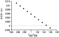
Fig. 4 illustrates the effect of the blue/red transmittance ratio of an exemplary LGP on color shift. As shown, the color shift Δ y increases approximately linearly as the blue light (450nm) transmittance decreases relative to the red light (630nm) transmittance. When the blue light transmittance reaches a value similar to the red light transmittance (e.g., the transmittance ratio is close to 1), the color shift Δ y is similarly close to 0. Fig. 5 presents a transmittance spectrum used to produce the correlation shown in fig. 4. Table I below provides details regarding light transmittance curves A-J.
Table I: curve of light transmittance
| Absorption Peak Displacement (Δ A) | Color shift (Δ y) | |
| A | 0.5 | 0.0111 |
| B | 0.4 | 0.0098 |
| C | 0.3 | 0.0084 |
| D | 0.2 | 0.0071 |
| E | 0.1 | 0.0057 |
| F | 0.0 | 0.0044 |
| G | -0.1 | 0.003 |
| H | -0.2 | 0.0017 |
| I | -0.3 | 0.0003 |
| J | -0.4 | -0.001 |
Since the polymer film may only account for a small fraction of the total thickness of the LGP, the blue/red transmittance ratio may be slightly lower than that shown in FIG. 4 (due to the relatively thin film) without significantly affecting the color shifting properties of the overall LGP. However, it may still be desirable to reduce blue light absorption and/or provide a more uniform absorption distribution throughout the visible wavelength range. In some embodiments, the polymer film may be selected to avoid the use of chromophores that absorb at wavelengths > 400nm, such as > 430nm or > 450 nm. In certain embodiments, the polymer film may be selected such that the concentration of blue light absorbing chromophore is less than about 5ppm, such as less than about 1ppm, less than about 0.5ppm, or less than about 0.1ppm, including all ranges and subranges therebetween. Alternatively, the polymer film may be modified to compensate for blue light absorption, for example by the addition of one or more dyes, pigments and/or brighteners which absorb at the yellow wavelength (e.g., -570-. However, processing the polymer material to have absorption at both blue and yellow wavelengths may reduce the overall light transmission of the film, thereby reducing the overall light transmission of the LGP. Thus, in certain embodiments, it may be advantageous to select and/or modify polymeric materials to reduce blue light absorption and thereby increase the overall light transmission of the film as an alternative. In some embodiments, the materials for the transparent substrate and the polymer film can be selected to have complementary optical absorption profiles, e.g., at a specified wavelength, such as blue wavelengths, the optical absorption of the glass substrate can balance or cancel the optical absorption of the polymer film such that the entire LGP does not exhibit any color shift.
According to various embodiments, the polymer film 120 can also be selected to have a refractive index dispersion that balances the interfacial fresnel reflection in the blue and red spectral regions such that the color shift along the length of the LGP is minimized. As shown in fig. 6, the glass substrate (G) may have substantially different refractive index dispersion compared to the polymer materials (P1-P4). The refractive index dispersion n (λ) for a given material can be modeled using the following equation:

where λ is the specified wavelength, a is the cauchy constant, and B and C are the coefficients of the specified material, determined by fitting equations to refractive indices measured at known wavelengths.
The mismatch in refractive index at a given wavelength can produce fresnel reflections at the glass-polymer interface of the LGP. In some embodiments, the degree of refractive index mismatch can be adjusted such that the wavelength-dependent Fresnel reflection coefficients of the layers minimize the net blue/red ratio variation of light propagating along the length of the LGP. For example, if the blue light reflectance is significantly higher than the red light reflectance, the blue light may be more strongly confined to the glass substrate and the light extraction features are less likely to extract the blue light.
Fig. 7 shows a simplified fresnel analysis of a glass substrate in which the polymer layers have different cauchy constants (a) and refractive index ranges. Fig. 7 illustrates that balancing the fresnel reflectivity of the glass-polymer interface over the wavelength range of interest minimizes the overall color shift. If the reflectivity is balanced between blue and red light, the color of the LGP will remain the same as the light repeatedly bounces along the length of the LGP. However, if blue light couples into the ink binder more efficiently than red light, the blue light will eventually deplete in the LGP, causing a yellow shift. In some embodiments, the LGP may have balanced interfacial fresnel reflections at 450nm (blue) and 650nm (red). For example, the difference in 45 Fresnel reflections at the substrate-polymer film interface may be less than about 0.04%, such as less than 0.035%, less than 0.03%, less than 0.025%, less than 0.02%, less than 0.015%, less than 0.005%, or less than 0.001%, including all ranges and subranges therebetween, for wavelengths between about 450-650 nm. Other relevant dispersion characteristics are described in co-pending U.S. provisional application No. 62/348,465 entitled "glazing articles COMPRISING LIGHT EXTRACTION FEATURES" (GLASS ARTICLES compact LIGHT EXTRACTION FEATURES) filed on 10.6.2016, the entire contents of which are incorporated herein by reference.
In certain embodiments, the substrate 110, the polymer film 120, the LGP 100, 100', 100 ", and/or the adhesive layer (if present) may be transparent or substantially transparent. As used herein, the term "transparent" means that the substrate, film, LGP or adhesive has a light transmittance of greater than about 80% in the visible region of the spectrum (420-750 nm) over a transmission length of 1mm or less. For example, in the visible range, exemplary transparent materials can have a light transmission of greater than about 85%, such as greater than about 90%, greater than about 95%, or greater than about 99%, including all ranges and subranges therebetween. In certain embodiments, an exemplary transparent material may have a light transmittance in the Ultraviolet (UV) region (100-400 nm) of greater than about 50%, such as greater than about 55%, greater than about 60%, greater than about 65%, greater than about 70%, greater than about 75%, greater than about 80%, greater than about 85%, greater than about 90%, greater than about 95%, or greater than about 99%, including all ranges and subranges therebetween.
In some embodiments, an exemplary transparent glass or polymer may comprise less than about 1ppm of each of Co, Ni, and Cr. In some embodiments, the concentration of Fe is < about 50ppm, less than < about 20ppm, or < about 10 ppm. In other embodiments, Fe +30Cr +35Ni < about 60ppm, Fe +30Cr +35Ni < about 40ppm, Fe +30Cr +35Ni < about 20ppm, or Fe +30Cr +35Ni < about 10 ppm. According to other embodiments, an exemplary transparent glass or polymer material may comprise a color shift ay <0.015, or in some embodiments, a color shift < 0.008.
The color shift can be characterized by: the change in x and y chromaticity coordinates of light extracted along the length L of an LGP illuminated with a standard white LED such as the Nichia (Nichia) NFSW157D-E was measured using the CIE 1931 color measurement standard. The nominal color point (color point) of the LED is chosen to be y 0.28 and x 0.29. For glass light guide plates, the color shift Δ y may be reported as Δ y ═ y (L)2)-y(L1) Wherein L is2And L1Is a Z position emitted away from the source along the panel or substrate direction, where L2-L10.5 m. An exemplary light guide plate has Δ y<0.05,Δy<0.01,Δy<0.005,Δy<0.003, or Δ y<0.001. If the LGP has no light extraction features, it can pass through at each measurement point L1And L2A small area of light extraction features is added for characterization.
The light scattering properties of the LGP can also be affected by the nominal refractive indices of the substrate and the polymeric material and the binder (if present). According to various embodiments, the nominal refractive index of the transparent substrate may be in the range of about 1.3 to about 1.8, such as about 1.35 to about 1.7, about 1.4 to about 1.65, about 1.45 to about 1.6, or about 1.5 to about 1.55, including all ranges and subranges therebetween. In some embodiments, the nominal refractive index of the polymeric material may be greater than the nominal refractive index of the substrate. In other embodiments, the nominal refractive index of the polymeric material may be substantially similar to the nominal refractive index of the substrate. If present, the adhesive layer may similarly have a nominal refractive index that is substantially similar to the nominal refractive index of the substrate and/or polymer film. As used herein, the term "nominal" refractive index refers to the refractive index near the peak of the human eye response (e.g., about 550 nm). As used herein, the term "substantially similar" means that two numerical values are approximately equal, for example within about 10% of each other, such as within about 5% of each other, or in some cases within about 2% of each other. For example, where the refractive index is 1.5, the substantially similar refractive index may be in the range of about 1.35 to about 1.65.
According to various non-limiting embodiments, the LGP (glass + polymer) may have a lower degree of light attenuation (e.g., due to absorption and/or scattering). For example, the total attenuation α' of LGP can be expressed as: α' ═ d1/D)*α1+(d2/D)*α2Wherein d is1Denotes the total thickness of the transparent substrate, d2Denotes the total thickness of the polymer film, D denotes the total thickness of the LGP (D ═ D)1+d2),α1Represents the attenuation value, alpha, of the transparent substrate2Representing the attenuation value of the polymer film. In some embodiments, the total attenuation α' may be less than about 5dB/m over the wavelength range of about 420-750 nm. For example, α' may be less than about 4dB/m, less than about 3dB/m, less than about 2dB/m, less than about 1dB/m, less than about 0.5dB/m, less than about 0.2dB/m, or less, including all ranges and subranges therebetween, such as about 0.2dB/m to about 5 dB/m.
The total attenuation of the LGP can be a function of, for example, the thickness of the polymer film and/or the ratio of the polymer film thickness to the total LGP thickness (d)2a/D) change. Thus, the polymer film thickness and/or the transparent substrate thickness may be varied to obtain a desired attenuation value. For example, (d)2/D) may be in the range of from about 1/2 to about 1/50, such as from about 1/3 to about 1/40, from about 1/5 to about 1/30, or from about 1/10 to about 1/20, including all ranges and subranges therebetween.
The LGPs disclosed herein may be used in various display devices, including but not limited to LCDs. According to aspects of the present disclosure, a display device may include at least one LGP disclosed herein connected to at least one light source that may emit blue, UV, or near UV light (e.g., about 100-500 nm). In some embodiments, the light source may be a Light Emitting Diode (LED). As an example of some components, the optical components of an exemplary LCD may further include a reflector, a diffuser, one or more prismatic films, one or more linear or reflective polarizers, a Thin Film Transistor (TFT) array, a liquid crystal layer, and one or more color filters. The LGPs disclosed herein may also be used in a variety of lighting devices, such as light fixtures or solid state lighting devices.
Method
Also disclosed herein is a method for forming a light guide plate, the method comprising: a layer of polymeric material is applied on a major surface of the transparent substrate and shaped to produce a plurality of microstructures patterned with a plurality of light extraction features. According to various embodiments, the method may include applying a layer of polymeric material on a major surface of the transparent substrate opposite the light emitting surface. In certain embodiments, the layer of polymeric material may be applied by screen printing. Shaping the polymeric material may be performed by, for example, microreplication, UV embossing, thermal embossing, or permanent embossing. The methods disclosed herein may also include one or more steps of forming a forming mold. The step of shaping the polymeric material may comprise applying a shaping mould to the layer of polymeric material.
Referring again to fig. 2, in various embodiments, the polymeric film 120 can be applied to the major surface 170 of the transparent substrate 110 by various methods including, for example, molding, printing, and/or lamination techniques. For example, a layer of polymeric material may be printed (e.g., screen printed, ink jet printed, slot coated, micro-printed, etc.), extruded, or otherwise coated onto a transparent substrate, and then embossed or embossed with a desired surface pattern. Alternatively, the polymeric material may be embossed or embossed in a desired pattern while the transparent substrate is coated with the polymeric material. These molding processes may be referred to as "microreplication," in which a mold is first formed in a desired pattern and then a polymeric material is pressed into the mold to create a negative replica of the shape of the mold. During or after imprinting, the polymer material may be UV-cured or thermally cured, which may be referred to as "UV embossing" and "thermal embossing". Alternatively, the polymer film may be applied using a thermal embossing technique, wherein the polymer material is first heated to a temperature above its glass transition point, and then embossed and cooled. In other non-limiting embodiments, the polymeric material may be applied as a film, for example laminated to the transparent substrate 110 with an intermediate adhesive layer.
Fig. 8A-D illustrate an exemplary method of forming a light guide plate that includes forming a molding die and then imprinting a polymeric material with the die. In fig. 8A, a first template 180 may be shaped or otherwise provided with a microstructure pattern 181. As shown in fig. 8B, first template 180 may be damaged, e.g., laser damaged, to produce a modified template 182 comprising light extraction features 183. As shown in fig. 8C, the second template may then be imprinted with the modified template 182 to produce a shaped mold 184. The molding die 184 may then be brought into contact with a layer of polymeric material coated on the transparent substrate 110 to produce the light guide plate 100 shown in fig. 8D, the light guide plate 100 comprising a polymeric film 120, the polymeric film 120 comprising a plurality of microstructures 130 patterned with a plurality of light extraction features 135.
Fig. 9A-H illustrate another exemplary method of forming a light guide plate that includes forming a molding die and then imprinting a polymeric material with the die. In fig. 9A, a first template 180 may be shaped or otherwise provided with a microstructure pattern 181. As shown in fig. 9B, the molding template may be imprint-molded with the first template 180 to form a negative template 185 comprising an inverted microstructure pattern 186. Referring to fig. 9C, a first material 187 is then applied to the negative template 185, for example deposited in the inverted microstructure pattern 186. At least a portion of the first material 187 may then be removed as shown, forming an inverse template 188 having an inverted microstructure pattern 186 and a temporary inverted light extraction pattern 189. For example, the first material 187 can comprise a photoresist material that can be selectively exposed to UV radiation 190 through a mask 191, as shown in fig. 9D, resulting in irradiated portions 192 and unexposed portions 193. As shown in fig. 9E, the unexposed portions 193 are then removed using photolithographic and/or etching techniques. Referring to fig. 9F, an intermediate template 194 may be imprinted with the inverted template 188, the intermediate template 194 having the microstructure pattern 181 and the light extraction pattern 183. The final target may then be imprinted with the intermediate template 194, resulting in the forming mold 184' shown in FIG. 9G. The molding die 184 'may then be brought into contact with a layer of polymeric material coated on the transparent substrate 110 to produce the light guide plate 100' shown in fig. 9H, the light guide plate 100 'comprising a polymeric film 120, the polymeric film 120 comprising a plurality of microstructures 130 patterned with a plurality of light extraction features 135'.
Also disclosed herein is a method for forming a light guide plate, the method comprising: a layer of polymeric material is applied on at least one major surface of the glass substrate and the polymeric material is modified to produce a plurality of light extraction features. In some embodiments, applying the layer of polymeric material may include adding a liquid resin to the substrate surface followed by UV or thermal curing of the resin to form a polymeric film. In other embodiments, applying the layer of polymeric material may include laminating the polymeric film to the substrate with an intermediate adhesive layer. After the polymer layer is applied, the polymer material may be modified, for example, by thermal and/or laser embossing, to create a plurality of light extraction features. The polymeric material may also optionally be shaped by, for example, microreplication, UV embossing, thermal embossing, or permanent embossing to create a plurality of microstructures.
Fig. 10 shows an exemplary LGP comprising a glass substrate laminated to a PET film (25 μm) by an optically clear adhesive (25 μm). The PET film was laser imprinted to produce an array of light extraction features. Although the exemplary light extraction features are shown as a periodic array, it should be understood that non-periodic arrays such as gradient patterns are also possible. For example, the light extraction features may be patterned to increase their density relative to increasing distance from the light source, as shown in FIG. 1C.
The methods disclosed herein can produce light extraction features 135, 135', 135 "of different shapes and sizes. For example, referring to fig. 11A-C, the method of fig. 4 can be performed, such as laser damaging the first template, to produce light extraction features having a profile that is graphically depicted. Scanning the laser light relative to the LGP in a raster pattern, or with a beam deflection system for more complex geometries, can produce an array of individual light extraction features. Exemplary lasers include, but are not limited to, Nd: YAG lasers, CO2A laser, etc. According to the required lightExtracting the feature profile changes the laser's operating parameters such as laser power, pulse duration, pulse energy, and other variables. In some embodiments, the pulse duration may be in the range of about 1 to about 1000 microseconds (μ β), such as about 5 to about 500 μ β, about 10 μ β to about 200 μ β, about 20 μ β to about 100 μ β, or about 30 μ β to about 50 μ β, including all ranges and subranges therebetween. The laser power may also be in the range of about 1 to about 100 watts (W), such as about 5 to about 50W, or about 10 to about 35W, including all ranges and subranges therebetween. The laser energy can be, for example, in the range of about 0.01 to about 100 millijoules (mJ), such as about 0.1 to about 10mJ, about 0.5 to about 5mJ, or about 1mJ to about 2mJ, including all ranges and subranges therebetween.
As shown in fig. 11A, a laser can be used to create a cratered light extraction feature, which can have a substantially parabolic cross-section, as shown in fig. 12A (see dashed lines). Alternatively, as shown in FIGS. 11B-C, a laser may be used to create conical light extraction features, which may have a substantially triangular cross-section, as shown in FIG. 12B (see dashed lines). Alternatively, the method described in fig. 9 can be performed, for example using photolithographic techniques, to produce truncated conical light extraction features, which can have a substantially trapezoidal cross-section, as shown in fig. 12C (see dashed lines). Of course, the light extraction features 135, 135', 135 "may have any other shape, cross-section, or combination thereof, all of which are intended to fall within the scope of the present disclosure. For example, in non-limiting embodiments, laser embossing can be used to create slit or grid shaped light extraction features in the polymer film that facilitate confining light propagating in the LGP to one or more channels. Such channels may be used in place of or in addition to microstructures to improve 1D or 2D dimming capability, such that only one (or more) of the light sources used contributes to the brightness of light in a given channel.
According to various embodiments, the transparent substrate may comprise a glass having a first glass transition temperature Tg1The first glass transition temperature Tg1Above the second glass transition temperature T of the polymer filmg2. For example, the difference in glass transition temperature (T)g1-Tg2) May be at least about 100 ℃, such as in the range of about 100 ℃ to about 800 ℃, about 200 ℃ to about 700 ℃, about 300 ℃ to about 600 ℃, or about 400 ℃ to about 500 ℃, including all ranges and subranges therebetween. This temperature difference allows the polymeric material to be molded onto the transparent substrate without melting or otherwise adversely affecting the transparent substrate during the molding process. In other embodiments, the transparent substrate may have a first melting temperature Tm1And/or a first viscosity v1Wherein the first melting temperature Tm1Above the second melting temperature T of the polymer filmm2A first viscosity v at a given processing temperature1Greater than the second viscosity v of the polymer film2。
It should be understood that the various embodiments disclosed may involve specific features, elements or steps which are described in connection with particular embodiments. It will also be understood that certain features, elements, or steps, although described in connection with a particular embodiment, may be interchanged or combined with alternative embodiments in various combinations or permutations not shown.
It is also to be understood that the words "a", "an", or "an" as used herein mean "at least one" and should not be limited to "only one" unless explicitly stated to the contrary. Thus, for example, reference to "a light source" includes examples having two or more such "light sources" unless the context clearly indicates otherwise. Similarly, "plurality" or "array" means "more than one". Thus, "a plurality of light scattering features" includes two or more such features, such as three or more such features, and so forth; "microstructure array" includes two or more such microstructures, such as three or more such microstructures, and the like.
Ranges may be expressed herein as from "about" one particular value, and/or to "about" another particular value. When such a range is expressed, examples include from the one particular value and/or to the other particular value. Similarly, when values are expressed as approximations, by use of the antecedent "about," it will be understood that the particular value forms another aspect. It will be further understood that the endpoints of each of the ranges are significant both in relation to the other endpoint, and independently of the other endpoint.
As used herein, the terms "substantially", "essentially" and variations thereof are intended to indicate that the feature is equivalent or substantially equivalent to a value or description. For example, a "substantially planar" surface is intended to designate a planar or substantially planar surface. Also, "substantially similar" is intended to indicate that two values are equal or approximately equal. In some embodiments, "substantially similar" may refer to values that differ from each other by about 10%, such as values that differ from each other by about 5% or values that differ from each other by about 2%.
Unless otherwise stated, it is not intended that any method described herein be construed as requiring that its steps be performed in a particular order. Thus, where a method claim does not actually recite an order to be followed by its steps or it does not otherwise specifically imply that the steps are to be limited to a specific order in the claims or specification, it is not intended that any particular order be implied.
Although the transition term "comprising" may be used to disclose various features, elements or steps of a particular embodiment, it should be understood that this implies that alternative embodiments may be included which may be described using the transition term consisting of, or consisting essentially of. Thus, for example, implied alternative embodiments to an apparatus comprising a + B + C include embodiments in which the apparatus consists of a + B + C and embodiments in which the apparatus consists essentially of a + B + C.
It will be apparent to those skilled in the art that various modifications and variations can be made in the present disclosure without departing from the spirit and scope of the disclosure. Since numerous modifications, combinations, sub-combinations and variations of the disclosed embodiments incorporating the spirit and substance of the disclosure may occur to persons skilled in the art, the disclosure should be construed to include everything within the scope of the appended claims and their equivalents.
The following examples are intended to be non-limiting and exemplary only, with the scope of the invention being defined by the claims.
Examples
With methyl Methacrylate Styrene (MS) or corning IrisTMGlass as a transparent substrate, light guide plates (692.2x 1212.4x 2mm) having various configurations were prepared. Microstructures and/or light extraction features are provided on one or both surfaces of the substrate as shown in table I below. When present, the polymer film matches the refractive index of the transparent substrate. An LED light source (120mm) was attached to the edge surface of the LGP. The configuration of example 1 is shown in FIG. 13A, and the configurations of examples 4 and 5 are shown in FIGS. 13B-C. The average surface luminance, luminance uniformity and color shift (Δ x, Δ y) were measured for each sample. The results of these measurements are listed in table I below. Fig. 14A-E show images of the light beams produced by each configuration. Finally, the normalized luminous flux from the LGP was measured as a function of distance from the LED centerline and plotted in FIG. 15.
Table I: LGP construction and measurements


Pattern 1: a light emitting surface; pattern 2: opposite main surface
As shown in table I above, the LGPs of examples 4-5 (containing patterned microstructures on the major surface opposite the light-emitting surface) exhibited comparable optical performance compared to the MS and glass LGPs (examples 1 and 3) having microstructures on the light-emitting surface and extraction features on the opposite major surface. The images shown in fig. 14A-E also reflect comparable local dimming efficiencies for these embodiments, where each of examples 1 and 3-5 exhibited a full width at half maximum (FWHM) value of 230mm (curve a in fig. 15), which was significantly narrower than the FHWM of 300mm for example 2, which example 2 had no microstructured surface (curve B in fig. 15).
With the methods disclosed herein, a single pre-fabricated mold can be utilized to provide both micro-structural and light extraction features at the surface of an LGP, which is simpler and/or more cost effective than the step of micro-structuring and printing the extraction features. Furthermore, microstructures and extraction features can be formed on a single surface of the LGP, enabling additional features to be formed on the opposite surface of the LGP. Finally, an LGP comprising a patterned microstructured surface as described above can have comparable optical performance and/or local dimming efficiency as compared to an LGP having microstructures on one surface and extraction features on the opposite surface.
Claims (34)
1. A light guide plate, comprising:
(a) a transparent substrate having an edge surface, a first major surface that emits light, and an opposing second major surface; and
(b) a polymeric film disposed on the second major surface of the transparent substrate, wherein the polymeric film comprises a plurality of microstructures patterned with a plurality of light extraction features, wherein the light extraction features are in the shape of slits or grids,
wherein a polymer film is laminated to a transparent substrate with an intermediate adhesive layer,
wherein the light guide plate has a color displacement Δ y less than 0.05, an
Wherein the transparent substrate is a glass substrate.
2. The light guide plate according to claim 1, wherein the glass substrate comprises, on a mole% oxide basis:
50-90 mol% SiO2,
0-20 mol% Al2O3,
0-20 mol% B2O3,
0-20 mol% P2O5And are and
0-25 mol% RxO,
Wherein x is 2 and R is selected from the group consisting of Li, Na, K, Rb, Cs and combinations thereof; or x is 1 and R is selected from the group consisting of Zn, Mg, Ca, Sr, Ba, and combinations thereof.
3. The light guide plate according to claim 1, wherein the transparent substrate contains less than 1ppm of each of Co, Ni and Cr.
4. The light guide plate according to claim 1, wherein the polymer film has a thickness d2In the range of 5 μm to 500 μm.
5. The light guide plate according to claim 1, wherein the polymer film comprises a UV-curable or a thermally-curable polymer.
6. The light guide plate according to claim 1, further comprising a second polymeric film disposed on the first major surface of the transparent substrate, the second polymeric film comprising a plurality of microstructures and/or a plurality of light extraction features.
7. The light guide plate of claim 1, wherein the plurality of microstructures comprises a periodic or aperiodic array of prisms, rounded prisms, or cylindrical lenses.
8. The light guide plate of claim 1, wherein at least one microstructure of the plurality of microstructures has an aspect ratio of 0.1 to 3.
9. The light guide plate according to claim 1, wherein at least one light extraction feature of the plurality of light extraction features has a dimension of less than 100 μ ι η.
10. A light guide assembly comprising at least one light source optically connected to the light guide plate of claim 1.
11. A display device, lighting device, or electronic device comprising the light guide plate of claim 1 or the light guide assembly of claim 10.
12. A method of forming a light guide plate, comprising:
(a) applying a layer of polymeric material to a major surface of a transparent substrate;
(b) shaping a polymeric material to produce a plurality of microstructures patterned with a plurality of light extraction features, wherein the light extraction features are in the shape of slits or grids,
wherein applying the layer of polymeric material comprises laminating a polymeric film to the major surface with an intermediate adhesive layer,
wherein the light guide plate has a color displacement Δ y less than 0.05, an
Wherein the transparent substrate is a glass substrate.
13. The method of claim 12, wherein the surface is a major surface opposite a light emitting surface of the transparent substrate.
14. The method of claim 12, wherein applying a layer of polymeric material comprises screen printing.
15. The method of claim 12, wherein shaping the polymeric material comprises microreplication, UV embossing, thermal embossing, or permanent embossing.
16. The method of claim 12, further comprising manufacturing a forming die by:
(a) laser damaging a first template comprising a microstructure pattern to produce a modified template comprising a light extraction pattern,
(b) and imprinting a second template with the modified template to form a molding die.
17. The method of claim 16, wherein shaping the polymeric material comprises applying a shaping mold to the layer of polymeric material.
18. The method of claim 12, further comprising creating a forming die by:
(a) imprinting a microstructure pattern into a molding template to form a negative template comprising an inverted microstructure pattern;
(b) applying a first material to a negative template;
(c) removing at least a portion of the first material to form a reverse template having a reverse microstructure pattern and a temporary reverse light extraction pattern;
(d) stamping the second template with a reverse template to form an intermediate template; and
(e) the third template is imprinted with the intermediate template to form a molding die.
19. The method of claim 18, wherein the first material is a photoresist material, a portion of which is selectively removed by a photolithographic technique.
20. The method of claim 18, wherein shaping the polymeric material comprises applying a shaping mold to the layer of polymeric material.
21. A light guide plate, comprising:
(a) a glass substrate having an edge surface, a first major surface that emits light, and an opposing second major surface; and
(b) a polymeric film disposed on at least one of the first major surface and the second major surface of the glass substrate, wherein the polymeric film comprises a plurality of light extraction features, wherein the light extraction features are in the shape of slits or grids,
wherein the polymer film is laminated to the glass substrate with an intermediate adhesive layer, and
wherein the light guide plate has a color displacement Δ y smaller than 0.05.
22. The light guide plate according to claim 21, wherein the polymer film has a thickness in a range of 5 μm to 500 μm.
23. The light guide plate according to claim 21, wherein the polymer film comprises a UV-curable or a thermally-curable polymer.
24. The light guide plate of claim 21, wherein the polymer film further comprises a plurality of microstructures.
25. The light guide plate of claim 24, wherein the plurality of microstructures comprises a periodic or aperiodic array of prisms, rounded prisms, or cylindrical lenses.
26. The light guide plate according to claim 21, wherein the polymer film has a nominal refractive index equal to the nominal refractive index of the glass substrate.
27. A light guide assembly comprising at least one light source optically connected to the light guide plate of claim 21.
28. The light guide assembly of claim 27, wherein the plurality of light extraction features are patterned and have an increased density relative to an increased distance from the at least one light source.
29. A display device, lighting device, or electronic device comprising the light guide plate of claim 21 or the light guide assembly of claim 28.
30. A method of forming a light guide plate, comprising:
(a) applying a layer of polymeric material to at least one major surface of a glass substrate; and
(b) modifying a polymer material to produce a plurality of light extraction features, wherein the light extraction features are in the shape of slits or grids,
wherein applying the layer of polymeric material comprises laminating a polymeric film to the at least one major surface with an intermediate adhesive layer, an
Wherein the light guide plate has a color displacement Δ y smaller than 0.05.
31. The method of claim 30, wherein applying the layer of polymeric material includes applying a liquid resin to the at least one major surface and UV or thermal curing the liquid resin.
32. The method of claim 30, wherein modifying the polymeric material comprises forming a pattern of light extraction features by laser embossing and/or hot embossing.
33. The method of claim 30, further comprising shaping the polymeric material with microreplication, UV relief, thermal relief, or permanent relief to create a plurality of microstructures.
34. The method of claim 33, wherein the plurality of microstructures comprises a periodic or aperiodic array of prisms, rounded prisms, or cylindrical lenses.
Applications Claiming Priority (3)
| Application Number | Priority Date | Filing Date | Title |
|---|---|---|---|
| US201662440029P | 2016-12-29 | 2016-12-29 | |
| US62/440,029 | 2016-12-29 | ||
| PCT/US2017/066923 WO2018125624A1 (en) | 2016-12-29 | 2017-12-18 | Microstructured and patterned light guide plates and devices comprising the same |
Publications (2)
| Publication Number | Publication Date |
|---|---|
| CN110140009A CN110140009A (en) | 2019-08-16 |
| CN110140009B true CN110140009B (en) | 2022-02-25 |
Family
ID=60937960
Family Applications (1)
| Application Number | Title | Priority Date | Filing Date |
|---|---|---|---|
| CN201780081835.6A Active CN110140009B (en) | 2016-12-29 | 2017-12-18 | Microstructured and patterned light guide plates and devices incorporating same |
Country Status (7)
| Country | Link |
|---|---|
| US (1) | US11022745B2 (en) |
| EP (1) | EP3563084A1 (en) |
| JP (1) | JP7046953B2 (en) |
| KR (1) | KR102534127B1 (en) |
| CN (1) | CN110140009B (en) |
| TW (1) | TW201838812A (en) |
| WO (1) | WO2018125624A1 (en) |
Families Citing this family (9)
| Publication number | Priority date | Publication date | Assignee | Title |
|---|---|---|---|---|
| KR20190015566A (en) * | 2016-06-10 | 2019-02-13 | 코닝 인코포레이티드 | Glass articles comprising light extraction features |
| KR102450088B1 (en) * | 2016-11-18 | 2022-10-05 | 코닝 인코포레이티드 | Microstructured light guide plate and device comprising same |
| FI128882B (en) * | 2017-12-22 | 2021-02-15 | Dispelix Oy | Optical waveguide and diffractive waveguide display |
| WO2020128707A1 (en) * | 2018-12-18 | 2020-06-25 | 3M Innovative Properties Company | Polymeric film having structured surface |
| US20200324694A1 (en) * | 2019-04-11 | 2020-10-15 | GM Global Technology Operations LLC | Edge-lit reading lamp including an anti-glare plate and a diffuser plate for reducing visible blue light |
| TWI723563B (en) | 2019-10-02 | 2021-04-01 | 明基材料股份有限公司 | Light bar structure |
| TWI714445B (en) * | 2020-01-22 | 2020-12-21 | 力晶積成電子製造股份有限公司 | Microlens strcuture and manufacturing method therefore |
| TWI765313B (en) * | 2020-08-10 | 2022-05-21 | 瑞儀光電股份有限公司 | Backlight module and display device therewith |
| FR3121236B1 (en) * | 2021-03-29 | 2024-02-09 | Optinvent | OPTICAL GUIDE AND CORRESPONDING MANUFACTURING METHOD |
Citations (4)
| Publication number | Priority date | Publication date | Assignee | Title |
|---|---|---|---|---|
| CN1797122A (en) * | 2004-12-31 | 2006-07-05 | Lg.菲利浦Lcd株式会社 | Backlight unit and liquid crystal display device having the same |
| CN101105606A (en) * | 2007-08-09 | 2008-01-16 | 友达光电股份有限公司 | Back light module group |
| CN203422542U (en) * | 2013-09-16 | 2014-02-05 | 陈文翰 | Liquid crystal display structure and electronic equipment |
| CN105705470A (en) * | 2013-11-08 | 2016-06-22 | 旭硝子株式会社 | Glass plate, light-guiding panel unit, planar light-emitting device, and liquid crystal display device |
Family Cites Families (56)
| Publication number | Priority date | Publication date | Assignee | Title |
|---|---|---|---|---|
| US6440880B2 (en) * | 1993-10-29 | 2002-08-27 | 3M Innovative Properties Company | Pressure-sensitive adhesives having microstructured surfaces |
| DE69504370T2 (en) * | 1994-11-29 | 1999-05-12 | Minnesota Mining & Mfg | TRANSPARENT DECORATIVE ITEM WITH AN ETCHED APPEARANCE AND PRISMATIC IMAGE |
| US5674790A (en) * | 1995-12-15 | 1997-10-07 | Corning Incorporated | Strengthening glass by ion exchange |
| US20100302479A1 (en) * | 1996-03-21 | 2010-12-02 | Aronson Joseph T | Optical article |
| JP2000036207A (en) | 1998-05-11 | 2000-02-02 | Meitaku System:Kk | Surface light source system |
| JPH11339527A (en) | 1998-05-22 | 1999-12-10 | Nichia Chem Ind Ltd | Forming method for light emitting device, liquid crystal display device, and light guide plate |
| US6752505B2 (en) * | 1999-02-23 | 2004-06-22 | Solid State Opto Limited | Light redirecting films and film systems |
| US7364341B2 (en) * | 1999-02-23 | 2008-04-29 | Solid State Opto Limited | Light redirecting films including non-interlockable optical elements |
| FR2802308B1 (en) | 1999-12-09 | 2002-03-08 | Gc Comm | LASER MACHINING METHOD AND DEVICE FOR LIGHT GUIDES, LIGHT GUIDES OBTAINED AND BACKLIGHT SCREENS INCORPORATING THESE GUIDES |
| US6777871B2 (en) * | 2000-03-31 | 2004-08-17 | General Electric Company | Organic electroluminescent devices with enhanced light extraction |
| JP2002116441A (en) * | 2000-10-06 | 2002-04-19 | Hitachi Ltd | Back light, method for manufacturing the same and liquid crystal display device which uses the same |
| US6703780B2 (en) * | 2001-01-16 | 2004-03-09 | General Electric Company | Organic electroluminescent device with a ceramic output coupler and method of making the same |
| KR100432438B1 (en) * | 2001-01-18 | 2004-05-22 | 주식회사 송산 | Prism Diffuser |
| JP2002350849A (en) * | 2001-05-25 | 2002-12-04 | Citizen Electronics Co Ltd | Front light of liquid crystal display device |
| JP3785093B2 (en) * | 2001-12-28 | 2006-06-14 | アルプス電気株式会社 | Light guide plate, manufacturing method therefor, lighting device, and liquid crystal display device |
| US7169722B2 (en) * | 2002-01-28 | 2007-01-30 | Guardian Industries Corp. | Clear glass composition with high visible transmittance |
| US6900941B2 (en) * | 2002-05-16 | 2005-05-31 | Eastman Kodak Company | Light diffuser with colored variable diffusion |
| US6818276B2 (en) * | 2002-10-24 | 2004-11-16 | Eastman Kodak Company | Light management film with colorant receiving layer |
| US20040234724A1 (en) * | 2003-05-22 | 2004-11-25 | Eastman Kodak Company | Immisible polymer filled optical elements |
| US8033706B1 (en) * | 2004-09-09 | 2011-10-11 | Fusion Optix, Inc. | Lightguide comprising a low refractive index region |
| WO2007002317A1 (en) * | 2005-06-23 | 2007-01-04 | Fusion Optix, Inc. | Enhanced diffusing plates, films and backlights |
| JP4316559B2 (en) * | 2005-11-30 | 2009-08-19 | 株式会社ナノクリエート | Light guide plate and manufacturing method thereof |
| KR100751519B1 (en) * | 2006-05-08 | 2007-08-23 | 미래나노텍(주) | Optical sheet and back light assembly of luquid crystal display equipped with the prism sheet |
| JP2009538516A (en) * | 2006-05-25 | 2009-11-05 | アイ2アイシー コーポレイション | Extraction of light with a preferred radiation pattern from a light emitting medium |
| US20080232135A1 (en) * | 2006-05-31 | 2008-09-25 | 3M Innovative Properties Company | Light guide |
| TWI328706B (en) * | 2006-08-18 | 2010-08-11 | Chimei Innolux Corp | Backlight module and liquid crystal display device |
| US7780330B2 (en) * | 2007-05-16 | 2010-08-24 | Rohm And Haas Electronics Materials Llc | Elongated illuminators configuration for LCD displays |
| US7991257B1 (en) * | 2007-05-16 | 2011-08-02 | Fusion Optix, Inc. | Method of manufacturing an optical composite |
| US20090040771A1 (en) * | 2007-08-08 | 2009-02-12 | Rohm And Haas Denmark Finance A/S | Thin light guiding plate and methods of manufacturing |
| WO2009051203A1 (en) * | 2007-10-19 | 2009-04-23 | Mitsubishi Rayon Co., Ltd., | Light guide member, method for producing the same and surface light source device using the same |
| US8619363B1 (en) * | 2007-11-06 | 2013-12-31 | Fusion Optix, Inc. | Light redirecting element comprising a forward diffracting region and a scattering region |
| DE102007062089A1 (en) * | 2007-12-21 | 2009-07-02 | Giesecke & Devrient Gmbh | Method for creating a microstructure |
| DE102007061979A1 (en) * | 2007-12-21 | 2009-06-25 | Giesecke & Devrient Gmbh | security element |
| US8851734B2 (en) * | 2008-03-27 | 2014-10-07 | Skc Haas Display Films Co., Ltd. | Light guiding film having light extraction features |
| DE102008031325A1 (en) * | 2008-07-02 | 2010-01-07 | Giesecke & Devrient Gmbh | Security element and method for its production |
| JP2010026280A (en) * | 2008-07-22 | 2010-02-04 | Hitachi Maxell Ltd | Liquid crystal display device |
| KR101040552B1 (en) * | 2008-11-06 | 2011-06-16 | 엘지전자 주식회사 | Optical Film, Backlight Unit And Liquid Crystal Display Device Comprising The Same |
| KR20100121861A (en) * | 2009-05-11 | 2010-11-19 | 삼성전자주식회사 | Light emitting unit and back light unit having the same |
| KR101683938B1 (en) * | 2009-06-02 | 2016-12-07 | 쓰리엠 이노베이티브 프로퍼티즈 컴파니 | Light redirecting film and display using this film |
| US20110244187A1 (en) * | 2010-04-06 | 2011-10-06 | Modilis Holdings Llc | Internal Cavity Optics |
| US8995059B2 (en) * | 2011-03-30 | 2015-03-31 | 3M Innovative Properties Company | Hybrid light redirecting and light diffusing constructions |
| US20140140091A1 (en) * | 2012-11-20 | 2014-05-22 | Sergiy Victorovich Vasylyev | Waveguide illumination system |
| US8944662B2 (en) * | 2012-08-13 | 2015-02-03 | 3M Innovative Properties Company | Diffractive luminaires |
| US8934173B2 (en) * | 2012-08-21 | 2015-01-13 | Svv Technology Innovations, Inc. | Optical article for illuminating building interiors with sunlight |
| US20140056029A1 (en) * | 2012-08-21 | 2014-02-27 | Shenzhen China Star Optoelectronics Technology Co. Ltd. | Backlight module |
| JP2015533228A (en) | 2012-10-08 | 2015-11-19 | コーニング インコーポレイテッド | Method and apparatus for providing improved display components |
| KR20150042937A (en) * | 2013-10-14 | 2015-04-22 | 삼성디스플레이 주식회사 | Optical sheet, methods of manufacturing the same and display devices including the same |
| US20150140156A1 (en) * | 2013-11-20 | 2015-05-21 | Thomas W. Palone | Non-deformable patterned template |
| KR102396551B1 (en) * | 2013-12-19 | 2022-05-12 | 코닝 인코포레이티드 | Textured surfaces for display applications |
| US10288792B2 (en) * | 2014-01-29 | 2019-05-14 | Corning Incorporated | Laser featured glass for display illumination |
| JP6575100B2 (en) * | 2015-03-25 | 2019-09-18 | 大日本印刷株式会社 | Light guide member, surface light source device, and display device |
| CN107533189B (en) * | 2015-04-24 | 2019-12-10 | 3M创新有限公司 | graded diffuser |
| KR20190015566A (en) | 2016-06-10 | 2019-02-13 | 코닝 인코포레이티드 | Glass articles comprising light extraction features |
| US20190146139A1 (en) | 2016-06-10 | 2019-05-16 | Corning Incorporated | Microstructured and patterned light guide plates and devices comprising the same |
| CN106094095A (en) * | 2016-08-12 | 2016-11-09 | 广州创维平面显示科技有限公司 | A kind of backlight module and liquid crystal display thereof |
| TWI655462B (en) * | 2018-07-04 | 2019-04-01 | Benq Materials Corporation | Polarizer |
-
2017
- 2017-12-18 JP JP2019534959A patent/JP7046953B2/en active Active
- 2017-12-18 US US16/474,460 patent/US11022745B2/en active Active
- 2017-12-18 KR KR1020197022319A patent/KR102534127B1/en active IP Right Grant
- 2017-12-18 WO PCT/US2017/066923 patent/WO2018125624A1/en unknown
- 2017-12-18 EP EP17826103.8A patent/EP3563084A1/en active Pending
- 2017-12-18 CN CN201780081835.6A patent/CN110140009B/en active Active
- 2017-12-29 TW TW106146453A patent/TW201838812A/en unknown
Patent Citations (5)
| Publication number | Priority date | Publication date | Assignee | Title |
|---|---|---|---|---|
| CN1797122A (en) * | 2004-12-31 | 2006-07-05 | Lg.菲利浦Lcd株式会社 | Backlight unit and liquid crystal display device having the same |
| CN101105606A (en) * | 2007-08-09 | 2008-01-16 | 友达光电股份有限公司 | Back light module group |
| CN203422542U (en) * | 2013-09-16 | 2014-02-05 | 陈文翰 | Liquid crystal display structure and electronic equipment |
| CN105705470A (en) * | 2013-11-08 | 2016-06-22 | 旭硝子株式会社 | Glass plate, light-guiding panel unit, planar light-emitting device, and liquid crystal display device |
| US10082616B2 (en) * | 2013-11-08 | 2018-09-25 | AGC Inc. | Glass plate, light guide plate unit, planar light-emitting device, and liquid crystal display device |
Also Published As
| Publication number | Publication date |
|---|---|
| TW201838812A (en) | 2018-11-01 |
| KR20190099060A (en) | 2019-08-23 |
| US20190339440A1 (en) | 2019-11-07 |
| CN110140009A (en) | 2019-08-16 |
| WO2018125624A1 (en) | 2018-07-05 |
| JP2020504424A (en) | 2020-02-06 |
| EP3563084A1 (en) | 2019-11-06 |
| KR102534127B1 (en) | 2023-05-18 |
| JP7046953B2 (en) | 2022-04-04 |
| US11022745B2 (en) | 2021-06-01 |
Similar Documents
| Publication | Publication Date | Title |
|---|---|---|
| CN110140009B (en) | Microstructured and patterned light guide plates and devices incorporating same | |
| US20190146139A1 (en) | Microstructured and patterned light guide plates and devices comprising the same | |
| US11092733B2 (en) | Microstructured light guide plates and devices comprising the same | |
| WO2017214482A1 (en) | Microstructured light guide plates and devices comprising the same | |
| CN111094842A (en) | Direct type backlight unit with 2D local dimming | |
| WO2018144720A1 (en) | Light guide assemblies comprising optical manipulation features | |
| TWI798359B (en) | Lcd backlight unit comprising a solvent free micro-replication resin | |
| KR20190044302A (en) | Microstructured light guide plates and methods of manufacture |
Legal Events
| Date | Code | Title | Description |
|---|---|---|---|
| PB01 | Publication | ||
| PB01 | Publication | ||
| SE01 | Entry into force of request for substantive examination | ||
| SE01 | Entry into force of request for substantive examination | ||
| GR01 | Patent grant | ||
| GR01 | Patent grant |