CN110045883B - Light beam direction control touch panel device - Google Patents
Light beam direction control touch panel device Download PDFInfo
- Publication number
- CN110045883B CN110045883B CN201811346137.7A CN201811346137A CN110045883B CN 110045883 B CN110045883 B CN 110045883B CN 201811346137 A CN201811346137 A CN 201811346137A CN 110045883 B CN110045883 B CN 110045883B
- Authority
- CN
- China
- Prior art keywords
- touch panel
- direction control
- beam direction
- electrode
- electrodes
- Prior art date
- Legal status (The legal status is an assumption and is not a legal conclusion. Google has not performed a legal analysis and makes no representation as to the accuracy of the status listed.)
- Active
Links
Images


Classifications
-
- G—PHYSICS
- G06—COMPUTING; CALCULATING OR COUNTING
- G06F—ELECTRIC DIGITAL DATA PROCESSING
- G06F3/00—Input arrangements for transferring data to be processed into a form capable of being handled by the computer; Output arrangements for transferring data from processing unit to output unit, e.g. interface arrangements
- G06F3/01—Input arrangements or combined input and output arrangements for interaction between user and computer
- G06F3/03—Arrangements for converting the position or the displacement of a member into a coded form
- G06F3/041—Digitisers, e.g. for touch screens or touch pads, characterised by the transducing means
- G06F3/0416—Control or interface arrangements specially adapted for digitisers
-
- G—PHYSICS
- G02—OPTICS
- G02F—OPTICAL DEVICES OR ARRANGEMENTS FOR THE CONTROL OF LIGHT BY MODIFICATION OF THE OPTICAL PROPERTIES OF THE MEDIA OF THE ELEMENTS INVOLVED THEREIN; NON-LINEAR OPTICS; FREQUENCY-CHANGING OF LIGHT; OPTICAL LOGIC ELEMENTS; OPTICAL ANALOGUE/DIGITAL CONVERTERS
- G02F1/00—Devices or arrangements for the control of the intensity, colour, phase, polarisation or direction of light arriving from an independent light source, e.g. switching, gating or modulating; Non-linear optics
- G02F1/29—Devices or arrangements for the control of the intensity, colour, phase, polarisation or direction of light arriving from an independent light source, e.g. switching, gating or modulating; Non-linear optics for the control of the position or the direction of light beams, i.e. deflection
-
- G—PHYSICS
- G06—COMPUTING; CALCULATING OR COUNTING
- G06F—ELECTRIC DIGITAL DATA PROCESSING
- G06F3/00—Input arrangements for transferring data to be processed into a form capable of being handled by the computer; Output arrangements for transferring data from processing unit to output unit, e.g. interface arrangements
- G06F3/01—Input arrangements or combined input and output arrangements for interaction between user and computer
- G06F3/03—Arrangements for converting the position or the displacement of a member into a coded form
- G06F3/041—Digitisers, e.g. for touch screens or touch pads, characterised by the transducing means
- G06F3/0412—Digitisers structurally integrated in a display
-
- G—PHYSICS
- G06—COMPUTING; CALCULATING OR COUNTING
- G06F—ELECTRIC DIGITAL DATA PROCESSING
- G06F3/00—Input arrangements for transferring data to be processed into a form capable of being handled by the computer; Output arrangements for transferring data from processing unit to output unit, e.g. interface arrangements
- G06F3/01—Input arrangements or combined input and output arrangements for interaction between user and computer
- G06F3/03—Arrangements for converting the position or the displacement of a member into a coded form
- G06F3/041—Digitisers, e.g. for touch screens or touch pads, characterised by the transducing means
- G06F3/0416—Control or interface arrangements specially adapted for digitisers
- G06F3/04166—Details of scanning methods, e.g. sampling time, grouping of sub areas or time sharing with display driving
-
- G—PHYSICS
- G06—COMPUTING; CALCULATING OR COUNTING
- G06F—ELECTRIC DIGITAL DATA PROCESSING
- G06F3/00—Input arrangements for transferring data to be processed into a form capable of being handled by the computer; Output arrangements for transferring data from processing unit to output unit, e.g. interface arrangements
- G06F3/01—Input arrangements or combined input and output arrangements for interaction between user and computer
- G06F3/03—Arrangements for converting the position or the displacement of a member into a coded form
- G06F3/041—Digitisers, e.g. for touch screens or touch pads, characterised by the transducing means
- G06F3/044—Digitisers, e.g. for touch screens or touch pads, characterised by the transducing means by capacitive means
- G06F3/0445—Digitisers, e.g. for touch screens or touch pads, characterised by the transducing means by capacitive means using two or more layers of sensing electrodes, e.g. using two layers of electrodes separated by a dielectric layer
-
- G—PHYSICS
- G06—COMPUTING; CALCULATING OR COUNTING
- G06F—ELECTRIC DIGITAL DATA PROCESSING
- G06F3/00—Input arrangements for transferring data to be processed into a form capable of being handled by the computer; Output arrangements for transferring data from processing unit to output unit, e.g. interface arrangements
- G06F3/01—Input arrangements or combined input and output arrangements for interaction between user and computer
- G06F3/03—Arrangements for converting the position or the displacement of a member into a coded form
- G06F3/041—Digitisers, e.g. for touch screens or touch pads, characterised by the transducing means
- G06F3/044—Digitisers, e.g. for touch screens or touch pads, characterised by the transducing means by capacitive means
- G06F3/0446—Digitisers, e.g. for touch screens or touch pads, characterised by the transducing means by capacitive means using a grid-like structure of electrodes in at least two directions, e.g. using row and column electrodes
-
- G—PHYSICS
- G09—EDUCATION; CRYPTOGRAPHY; DISPLAY; ADVERTISING; SEALS
- G09G—ARRANGEMENTS OR CIRCUITS FOR CONTROL OF INDICATING DEVICES USING STATIC MEANS TO PRESENT VARIABLE INFORMATION
- G09G3/00—Control arrangements or circuits, of interest only in connection with visual indicators other than cathode-ray tubes
- G09G3/20—Control arrangements or circuits, of interest only in connection with visual indicators other than cathode-ray tubes for presentation of an assembly of a number of characters, e.g. a page, by composing the assembly by combination of individual elements arranged in a matrix no fixed position being assigned to or needed to be assigned to the individual characters or partial characters
- G09G3/34—Control arrangements or circuits, of interest only in connection with visual indicators other than cathode-ray tubes for presentation of an assembly of a number of characters, e.g. a page, by composing the assembly by combination of individual elements arranged in a matrix no fixed position being assigned to or needed to be assigned to the individual characters or partial characters by control of light from an independent source
- G09G3/3433—Control arrangements or circuits, of interest only in connection with visual indicators other than cathode-ray tubes for presentation of an assembly of a number of characters, e.g. a page, by composing the assembly by combination of individual elements arranged in a matrix no fixed position being assigned to or needed to be assigned to the individual characters or partial characters by control of light from an independent source using light modulating elements actuated by an electric field and being other than liquid crystal devices and electrochromic devices
- G09G3/344—Control arrangements or circuits, of interest only in connection with visual indicators other than cathode-ray tubes for presentation of an assembly of a number of characters, e.g. a page, by composing the assembly by combination of individual elements arranged in a matrix no fixed position being assigned to or needed to be assigned to the individual characters or partial characters by control of light from an independent source using light modulating elements actuated by an electric field and being other than liquid crystal devices and electrochromic devices based on particles moving in a fluid or in a gas, e.g. electrophoretic devices
-
- G—PHYSICS
- G02—OPTICS
- G02F—OPTICAL DEVICES OR ARRANGEMENTS FOR THE CONTROL OF LIGHT BY MODIFICATION OF THE OPTICAL PROPERTIES OF THE MEDIA OF THE ELEMENTS INVOLVED THEREIN; NON-LINEAR OPTICS; FREQUENCY-CHANGING OF LIGHT; OPTICAL LOGIC ELEMENTS; OPTICAL ANALOGUE/DIGITAL CONVERTERS
- G02F2201/00—Constructional arrangements not provided for in groups G02F1/00 - G02F7/00
- G02F2201/12—Constructional arrangements not provided for in groups G02F1/00 - G02F7/00 electrode
-
- G—PHYSICS
- G09—EDUCATION; CRYPTOGRAPHY; DISPLAY; ADVERTISING; SEALS
- G09G—ARRANGEMENTS OR CIRCUITS FOR CONTROL OF INDICATING DEVICES USING STATIC MEANS TO PRESENT VARIABLE INFORMATION
- G09G2300/00—Aspects of the constitution of display devices
- G09G2300/02—Composition of display devices
- G09G2300/023—Display panel composed of stacked panels
-
- G—PHYSICS
- G09—EDUCATION; CRYPTOGRAPHY; DISPLAY; ADVERTISING; SEALS
- G09G—ARRANGEMENTS OR CIRCUITS FOR CONTROL OF INDICATING DEVICES USING STATIC MEANS TO PRESENT VARIABLE INFORMATION
- G09G2320/00—Control of display operating conditions
- G09G2320/06—Adjustment of display parameters
- G09G2320/068—Adjustment of display parameters for control of viewing angle adjustment
-
- G—PHYSICS
- G09—EDUCATION; CRYPTOGRAPHY; DISPLAY; ADVERTISING; SEALS
- G09G—ARRANGEMENTS OR CIRCUITS FOR CONTROL OF INDICATING DEVICES USING STATIC MEANS TO PRESENT VARIABLE INFORMATION
- G09G2354/00—Aspects of interface with display user
-
- G—PHYSICS
- G09—EDUCATION; CRYPTOGRAPHY; DISPLAY; ADVERTISING; SEALS
- G09G—ARRANGEMENTS OR CIRCUITS FOR CONTROL OF INDICATING DEVICES USING STATIC MEANS TO PRESENT VARIABLE INFORMATION
- G09G2358/00—Arrangements for display data security
Abstract
The present invention relates to a beam direction control touch panel device, comprising: an upper beam direction control electrode and an upper touch panel electrode disposed on a lower surface of the upper transparent substrate; a lower touch panel electrode disposed on an upper surface of the lower transparent substrate; an electrophoresis element interposed between the upper beam direction control electrode and the lower touch panel electrode; a light-transmitting region surrounded by the electrophoretic element and interposed between the upper transparent substrate and the lower transparent substrate; and a controller, each of the upper beam direction control electrodes including an opening overlapping the light-transmitting region, the controller providing a driving potential to the lower touch panel electrode in a capacitance measurement for detecting a touch position, and providing the driving potential to the upper beam direction control electrode based on the driving potential provided to the lower touch panel electrode.
Description
Technical Field
The present invention relates to a beam direction control touch panel device.
Background
In recent years, in the context of widespread use of smartphones and tablet devices, touch panels are increasingly widely regarded as user interfaces with high usability. Touch panels are used for display units of various electronic devices. In smartphones, ATM, on-board entertainment displays, etc., viewing angle control devices are used so that the displayed content is not easily seen by others than the user.
When the touch panel and the viewing angle controlling device are separately mounted on the display panel, the total thickness of the display device will increase due to the thickness of each component. In a structure in which the viewing angle control device is interposed between the touch panel and the display panel, the distance between the touch panel and the display panel becomes large, which deteriorates operability. In addition, since there will be more interfaces with an air layer in the display device, surface reflection of external light may deteriorate visibility.
Patent document 1 (WO 2006/030745) discloses a display device equipped with a touch panel that can control a viewing angle. Specifically, patent document 1 discloses a display device using a first transparent electrode film for a touch panel, the first transparent electrode film being a component of an SW-LCD that controls a viewing angle, the display device having a position detection device configured to detect currents flowing from a plurality of positions on the first transparent electrode film when an object touches a surface of the first transparent electrode film, and to detect a touch position of the object based on a detection result.
On the other hand, patent document 2 (japanese patent application laid-open publication No. 2016-62091) discloses a beam direction control device configured to electrically control a viewing angle by using an electrophoretic element.
Disclosure of Invention
The touch panel of patent document 1 adopts a surface electrostatic capacitance method, and thus it is difficult to realize a multi-touch function. If the touch panel and the viewing angle control device capable of electrically controlling the viewing angle are integrally formed and share a common substrate, the total thickness of the display device can be reduced, and a display device having excellent visibility and usability of the touch panel can be provided. In order to achieve this, a technology of integrating a touch panel having a multi-touch function and a viewing angle control device that can electrically control a viewing angle to share a common substrate is required.
The light beam direction control touch panel device of the present invention includes: an upper transparent substrate; a lower transparent substrate; a plurality of upper beam direction control electrodes and a plurality of upper touch panel electrodes alternately disposed on a lower surface of the upper transparent substrate in a first direction; a plurality of lower touch panel electrodes disposed on an upper surface of the lower transparent substrate and facing the upper beam direction control electrodes; a plurality of electrophoretic elements interposed between the plurality of upper beam direction control electrodes and the plurality of lower touch panel electrodes, the plurality of electrophoretic elements respectively including colored electrophoretic particles and a dispersion medium; a plurality of light-transmitting regions interposed between the upper transparent substrate and the lower transparent substrate, the plurality of light-transmitting regions being surrounded by the electrophoretic element; and a controller, the plurality of upper beam direction control electrodes each including an opening that positionally overlaps the light-transmitting region, the controller configured to: providing a driving potential to the plurality of lower touch panel electrodes in capacitance measurement for detecting touch positions, thereby forming electric fields from the plurality of lower touch panel electrodes to the plurality of upper touch panel electrodes via the openings; and supplying a driving potential to the plurality of upper beam direction control electrodes according to the driving potential supplied to the plurality of lower touch panel electrodes, thereby switching between a dispersed state and a concentrated state of the colored electrophoretic particles in the plurality of electrophoretic elements.
It is to be understood that both the foregoing general description and the following detailed description are exemplary and explanatory only and are not restrictive of the invention.
According to an embodiment of the present invention, it is possible to provide a beam direction control touch panel having a touch panel integrally formed with a viewing angle control device that can electrically control a viewing angle so as to share a common substrate, and having a multi-touch function.
Drawings
The invention may be understood from the following description taken in conjunction with the accompanying drawings in which:
fig. 1 is a sectional view schematically showing a structural example of a display device according to embodiment 1;
fig. 2 is a plan view schematically showing a structural example of an upper electrode according to embodiment 1;
fig. 3 is a plan view schematically showing a structural example of a lower electrode according to embodiment 1;
fig. 4 is a cross-sectional view showing an example of a cross-sectional structure of the beam direction control touch panel in a wide view angle state, taken along line AA' of fig. 2 and 3;
fig. 5 is a sectional view showing an example of a sectional structure of the beam direction control touch panel taken along line BB' of fig. 2 and 3;
fig. 6 is a cross-sectional view showing an example of a cross-sectional structure of the beam direction control touch panel taken along the line CC' of fig. 2 and 3;
Fig. 7 is a perspective view schematically showing a structural example of a beam direction control touch panel according to embodiment 1;
fig. 8 is a block diagram schematically showing an example of the logical structure of a control system for controlling a touch panel in the beam direction according to embodiment 1;
fig. 9 is a diagram schematically showing waveforms of driving signals supplied to the respective electrodes in a wide viewing angle state;
fig. 10A shows an example of waveforms of driving potentials (driving signals) supplied to the lower electrode in the mutual capacitance mode and the wide viewing angle mode according to embodiment 1;
fig. 10B shows an example of waveforms of driving potentials (driving signals) supplied to the upper electrodes in the mutual capacitance mode and the wide viewing angle mode according to embodiment 1;
fig. 11A shows an example of waveforms of driving potentials (driving signals) supplied to the lower electrode in the self-capacitance mode and the wide viewing angle mode according to embodiment 1;
fig. 11B shows an example of waveforms of driving potentials (driving signals) supplied to the upper electrode in the self-capacitance mode and the wide viewing angle mode according to embodiment 1;
fig. 12 is a cross-sectional view showing an example of a cross-sectional structure of a light beam direction control touch panel in a narrow view angle state according to embodiment 1;
Fig. 13 is a diagram schematically showing waveforms of driving signals supplied to the respective electrodes in a narrow viewing angle state according to embodiment 1;
fig. 14A shows an example of waveforms of driving potentials (driving signals) supplied to the lower electrode in the mutual capacitance mode and the narrow viewing angle mode according to embodiment 1;
fig. 14B shows an example of waveforms of driving potentials (driving signals) supplied to the upper electrodes in the mutual capacitance mode and the narrow viewing angle mode according to embodiment 1;
fig. 15A shows an example of waveforms of driving potentials (driving signals) supplied to the lower electrode in the self-capacitance mode and the narrow viewing angle mode according to embodiment 1;
fig. 15B shows an example of waveforms of driving potentials (driving signals) supplied to the upper electrode in the self-capacitance mode and the wide viewing angle mode according to embodiment 1;
fig. 16 is a diagram schematically showing waveforms of driving signals supplied to the respective electrodes in a wide viewing angle state according to embodiment 2;
fig. 17 shows an example of waveforms of driving potentials (driving signals) supplied to the lower electrode in the mutual capacitance mode and the wide viewing angle mode according to embodiment 2;
fig. 18A shows an example of waveforms of driving potentials (driving signals) supplied to the lower electrode in the self-capacitance mode and the wide viewing angle mode according to embodiment 2;
Fig. 18B shows an example of waveforms of driving potentials (driving signals) supplied to the upper electrode in the self-capacitance mode and the wide viewing angle mode according to embodiment 2;
fig. 19 is a plan view schematically showing a structural example of an upper electrode according to embodiment 3;
fig. 20 is a cross-sectional view showing an example of a cross-sectional structure of the beam direction control touch panel in a wide view angle state, taken along line AA' of fig. 19;
fig. 21 is a sectional view showing an example of a sectional structure of the beam direction control touch panel taken along line BB' of fig. 19;
fig. 22 is a sectional view showing an example of a sectional structure of the beam direction control touch panel taken along the line CC' of fig. 19;
fig. 23 is a cross-sectional view showing an example of a cross-sectional structure of a light beam direction control touch panel in a wide view angle state according to embodiment 3;
fig. 24 is a plan view schematically showing a structural example of upper electrode 6 according to embodiment 4;
fig. 25 is a plan view schematically showing a structural example of a lower electrode according to embodiment 4;
fig. 26 is a sectional view showing an example of a sectional structure of the beam direction control touch panel in a wide view angle state taken along line AA' of fig. 24 and 25; and
Fig. 27 is a sectional view showing an example of a sectional structure of the light beam direction control touch panel in a wide view angle state taken along line BB' of fig. 24 and 25.
Detailed Description
Hereinafter, embodiments of the present invention will be described in detail with reference to the accompanying drawings. These embodiments of the present invention are merely examples for implementing the present invention and should not be construed as limiting the technical scope of the present invention. Like structures are denoted by like reference numerals throughout the drawings. The size and shape of the illustrated components and structures need not be true for ease of illustration.
The beam direction control touch panel disclosed below includes an upper transparent substrate, a lower transparent substrate, and an electrophoretic element disposed between the upper transparent electrode and the lower transparent electrode. The electrophoretic element includes colored electrophoretic particles having surface charges and light shielding characteristics, and a translucent dispersion medium. The beam direction control touch panel has a narrow viewing angle mode and a wide viewing angle mode. In the narrow viewing angle mode, the colored electrophoretic particles are dispersed in a dispersion medium. On the other hand, in the wide viewing angle mode, the colored electrophoretic particles are concentrated at a specific position.
An upper electrode is provided on a lower surface of the upper transparent substrate (or in other words, a surface facing the lower transparent substrate). The upper electrode includes an upper touch panel electrode for detecting a touch position and an upper beam direction control electrode for controlling a beam direction. The upper beam direction control electrode has an opening formed therein.
A lower electrode is provided on an upper surface of the lower transparent substrate (or in other words, a surface facing the upper transparent substrate). The lower electrode includes a lower touch panel electrode that faces the upper beam direction control electrode and receives a signal (potential) that enables the touch panel to function. The lower electrode further includes a lower beam direction control electrode facing the upper touch panel electrode and configured to control a beam direction.
The electrophoresis element is sandwiched between the upper electrode and the lower electrode. The controller supplies a driving potential to each touch panel electrode in capacitance measurement for detecting a touch position, and supplies a potential to the beam direction control electrode according to the driving potential. In this way, the state of the colored electrophoretic particles can be maintained to achieve a desired viewing angle pattern while detecting the touch position.
The lower touch panel electrode is supplied with a signal (potential) to realize a touch panel function. In this state, if the object touches the upper transparent substrate, an electric field is formed from the lower touch panel electrode to the upper touch panel electrode via the opening of the upper beam direction control electrode facing the lower touch panel electrode. The touch panel function is enabled by the electric field.
As described above, each touch panel electrode also serves as a beam direction control electrode. Therefore, it is necessary to supply a potential to each beam direction control electrode according to the potential of each touch panel electrode to appropriately control the electrophoretic element.
In order to make each touch panel electrode double as a touch panel part and a light control panel part, the light beam direction control touch panel adopts a projection type electrostatic capacitance method (projection electrostatic capacity method). In a touch panel of the projected capacitance method, a touch position of an object is detected by recognizing a change in capacitance between an electrode and the object.
< Structure >
Fig. 1 is a sectional view schematically showing a structural example of a display device. Fig. 2 is a plan view schematically showing a structural example of the upper electrode. Fig. 3 is a plan view schematically showing a structural example of the lower electrode. The display device includes a display panel 5 and a beam direction control touch panel 1 disposed in front of the display panel 5. The display panel 5 may be of any type. Examples of the display panel 5 include a liquid crystal display panel and an OLED (organic light emitting diode) display panel.
In this specification, a side closer to a user viewing an image on the display panel 5 is referred to as an upper side, or in other words, a side toward which a light beam of the image travels is referred to as an upper side, and an opposite side is referred to as a rear side or a lower side. In addition, directions perpendicular to the main surfaces of the display panel 5 and the light flux direction control touch panel 1 are Z-axis directions, and two directions perpendicular to each other and horizontal to the main surfaces are an X-axis direction (first direction) and a Y-axis direction (second direction), respectively. The Z-axis direction is the direction in which the display panel 5 and the beam direction control touch panel 1 are stacked.
The light flux direction control touch panel 1 has a touch panel function and a function of controlling the direction of a light flux passing through the light flux direction control touch panel 1 among light fluxes from the display panel 5. The beam direction control touch panel 1 can allow an image of the display panel 5 to pass therethrough, switching between a wide viewing angle mode and a narrow viewing angle mode. A state (mode) in which the range of the output direction from the light flux direction control touch panel 1 is wide is referred to as a wide viewing angle state (wide viewing angle mode), and a state (mode) in which the range of the output direction is narrow is referred to as a narrow viewing angle state (narrow viewing angle mode).
In the example of fig. 1, the beam direction control touch panel 1 is in a wide viewing angle state. In the beam direction control touch panel 1, the state of the colored electrophoretic particles (colored charged particles) is changed, thereby adjusting the range of the output direction of light passing through the light transmitting region 15 and the dispersion medium.
The beam direction control touch panel 1 is adhered to the front surface (upper surface) of the display panel 5 by, for example, an adhesive layer. The adhesive layer between the beam direction controlling touch panel 1 and the display panel 5 may be omitted. Alternatively, an air gap or any optical film may be provided between the beam direction control touch panel 1 and the display panel 5.
The beam direction control touch panel 1 includes an upper transparent substrate 11 and a lower transparent substrate 17. The lower surface of the lower transparent substrate 17 faces the display panel 5, and the upper surface of the lower transparent substrate 17 faces the lower surface of the upper transparent substrate. The upper transparent substrate 11 and the lower transparent substrate 17 are each formed of a light-transmitting material such as glass, PET (polyethylene terephthalate), PC (polycarbonate), or PEN (polyethylene naphthalate). The upper transparent substrate 11 and the lower transparent substrate 17 are each an inflexible insulator or a flexible insulator.
The beam direction control touch panel 1 further includes an upper electrode 6 provided on the lower surface of the upper transparent substrate 11 and a lower electrode 7 provided on the upper surface of the lower transparent substrate 17. As shown in fig. 2, the upper electrode 6 is constituted by a plurality of upper touch panel electrodes 12 and a plurality of upper beam direction control electrodes 18. As shown in fig. 3, the lower electrode 7 is constituted by a plurality of lower touch panel electrodes 13 and a plurality of lower beam direction control electrodes 16. The upper touch panel electrode 12, the upper beam direction control electrode 18, the lower touch panel electrode 13, and the lower beam direction control electrode 16 are transparent electrodes, and are made of, for example, ITO (indium tin oxide), znO, or IGZO.
The plurality of lower beam direction control electrodes 16 (lower beam direction control electrode patterns) extend in the X-axis direction on the lower transparent substrate 17, respectively, and are arranged at regular intervals in the Y-axis direction. For example, each of the lower beam direction control electrodes 16 has a shape in which a plurality of diamond (or square) electrode pieces are connected to each other, the plurality of electrode pieces being arranged in the same orientation in the X-axis direction (e.g., such that each vertex faces the X-axis direction or the Y-axis direction).
The plurality of lower touch panel electrodes 13 (lower touch panel electrode patterns) extend in the X-axis direction on the lower transparent substrate 17, respectively, and are arranged at regular intervals in the Y-axis direction. For example, as in the case of the lower beam direction control electrode 16, each lower touch panel electrode 13 has a shape in which a plurality of diamond-shaped (or square-shaped) electrode pieces are connected to each other, the plurality of electrode pieces being arranged in the same orientation in the X-axis direction (for example, such that each vertex faces the X-axis direction or the Y-axis direction). As described in detail later, the lower touch panel electrode 13 also functions as a beam direction control electrode.
The lower beam direction control electrodes 16 and the lower touch panel electrodes 13 are alternately arranged in the Y-axis direction. For example, each lower beam direction control electrode 16 and each lower touch panel electrode 13 adjacent to each other are arranged with a gap therebetween. The gap between the lower beam direction control electrode 16 and the lower touch panel electrode 13 may be filled with an insulating material (e.g., silicon nitride), or remain unfilled. As described in detail later, the lower touch panel electrode 13 also functions as a beam direction control electrode.
The plurality of upper touch panel electrodes 12 (upper touch panel electrode patterns) extend in the Y-axis direction on the upper transparent substrate 11, respectively, and are arranged at regular intervals in the X-axis direction. For example, each upper touch panel electrode 12 has a shape in which a plurality of diamond-shaped (or square-shaped) electrode pieces are connected to each other, the plurality of electrode pieces being arranged in the same orientation in the Y-axis direction (e.g., such that each vertex faces the X-axis direction or the Y-axis direction). In this embodiment, each electrode piece of the upper touch panel electrode 12 faces a corresponding electrode piece of the lower beam direction control electrode 16. For example, the electrode sheets facing each other have substantially the same shape and substantially the same size. As described in detail later, the upper touch panel electrode 12 also functions as a beam direction control electrode.
The plurality of upper beam direction control electrodes 18 (upper beam direction control electrode patterns) extend in the Y-axis direction on the upper transparent substrate 11, respectively, and are arranged at regular intervals in the X-axis direction. For example, in the same manner as the upper touch panel electrode 12, each upper beam direction control electrode 18 has a shape in which a plurality of diamond-shaped (or square-shaped) electrode pieces are connected to each other, the plurality of electrode pieces being arranged in the same orientation in the Y-axis direction (e.g., such that each vertex faces the X-axis direction or the Y-axis direction). In this embodiment, each electrode piece of the upper beam direction control electrode 18 faces a corresponding electrode piece of the lower touch panel electrode 13. For example, the electrode sheets facing each other have substantially the same shape and substantially the same size.
The upper beam direction control electrodes 18 and the upper touch panel electrodes 12 are alternately arranged in the X-axis direction. For example, each upper beam direction control electrode 18 and each upper touch panel electrode 12 adjacent to each other are arranged with a gap therebetween. The gap between the upper beam direction control electrode 18 and the upper touch panel electrode 12 may be filled with an insulating material (e.g., silicon nitride), or remain unfilled.
An opening 181 is formed in the upper beam direction control electrode 18. In the example of fig. 2, each electrode piece of the upper beam direction control electrode 18 has a plurality of openings 181 of a rectangular shape in which the Y-axis direction is the length direction. The shape of the opening 181 is not limited to a rectangular shape, and the opening 181 may be formed in any shape.
The beam direction control touch panel 1 includes a beam direction control layer between the upper transparent substrate 11 and the lower transparent substrate 17. The beam direction control layer is composed of a plurality of electrophoretic elements 14 and a plurality of light-transmitting regions 15. The electrophoretic elements 14 and the light-transmitting regions 15 extend in the Y-axis direction, respectively, and are alternately arranged in the X-axis direction.
In the XY plane, the plurality of electrophoretic elements 14 have a stripe pattern in which each electrophoretic element extends in the Y-axis direction and is arranged in the X-axis direction. Also, the plurality of light-transmitting regions 15 have a stripe pattern in which each light-transmitting region extends in the Y-axis direction and is aligned in the X-axis direction.
The height of the light-transmitting region 15 is, for example, 3 μm to 300 μm. The width of the light-transmitting region 15 is, for example, 1 μm to 150 μm, and the pitch of the light-transmitting region 15 is, for example, 0.25 μm to 40 μm. The widths of the upper touch panel electrode 12, the upper beam direction control electrode 18, the lower touch panel electrode 13, and the lower beam direction control electrode 16 are, for example, 5 μm to 10 μm if the material is metal, and are, for example, about 100 μm if the material is ITO. The pitches of the upper touch panel electrode 12, the upper beam direction control electrode 18, the lower touch panel electrode 13, and the lower beam direction control electrode 16 are, for example, several millimeters (specifically, about 5 mm).
Each of the electrophoretic elements 14 includes electrophoretic particles contained in a space formed between the light-transmitting regions 15, and a dispersion medium (electrophoretic element material). The electrophoretic particles are coloured and the colour is for example black. The dispersion medium is formed of a transparent liquid material.
Each electrophoretic element is sandwiched between an upper electrode 6 and a lower electrode 7. In the example of fig. 1, the upper electrode 6 and the lower electrode 7 contact an electrophoretic element material made of electrophoretic particles and a dispersion medium. An insulating layer may be formed between the electrophoretic element material and one or both of the upper electrode 6 and the lower electrode 7. The insulating layer is made of, for example, silicon oxide or silicon nitride.
In the example of fig. 1, the beam direction control touch panel 1 is in a wide viewing angle state. For example, the wide viewing angle state is achieved by concentrating the electrophoretic particles near one of the electrodes (or in other words, the lower electrode 7) sandwiching the electrophoretic element 14. In this case, most of the electrophoretic element 14 includes only a transparent dispersion medium, which allows light to pass through the electrophoretic element 14. As a result, the light beam having a wide range of output angles in the X-axis direction passes through the light beam direction control touch panel 1.
In the wide viewing angle state, the relative potential (potential difference V) of the lower electrode 7 with respect to the upper electrode 6 has a polarity opposite to the charge of the electrophoretic particles. This causes the electrophoretic particles to concentrate near the lower electrode 7.
For example, when the charge of the electrophoretic particles is negative (-), the lower electrode 7 and the upper electrode 6 are applied with a potential such that the lower electrode 7 has a positive polarity. For example, when the charge of the electrophoretic particles is positive (+) the lower electrode 7 and the upper electrode 6 are applied such that the lower electrode 7 has a potential of a negative polarity. In the following description, the charge of the electrophoretic particles is negative. If the charge of the electrophoretic particles is positive, the same structure can be applied by reversing the polarity of the lower electrode 7.
On the other hand, in the narrow viewing angle state, the electrophoretic particles in each electrophoretic element 14 are dispersed in a dispersion medium. The dispersed electrophoretic particles absorb light from the display panel 5, which causes the electrophoretic element 14 to block light from the display panel 5. As a result, the light beam having a narrower range of output angles in the X-axis direction passes through the light beam direction control touch panel 1.
In the narrow viewing angle state, the electric potentials of the upper electrode 6 and the lower electrode 7 sandwiching each electrophoretic element 14 are maintained the same. In this way, the electrophoretic particles remain dispersed in the dispersion medium. The upper electrode 6 is configured to receive a specific signal for a touch panel function. How the potentials of the upper electrode 6 and the lower electrode 7 are controlled is described in detail below.
Fig. 4 is a sectional view showing an example of a sectional structure of the beam direction control touch panel 1 in a wide view angle state taken along the line A-A' of fig. 2 and 3. Fig. 5 is a sectional view showing an example of a sectional structure of the beam direction control touch panel 1 taken along a line BB' of fig. 2 and 3. Fig. 6 is a sectional view showing an example of a sectional structure of the beam direction control touch panel 1 taken along a line CC' of fig. 2 and 3.
The opening 181 formed in the upper beam direction control electrode 18 is formed to overlap in position with the light transmitting region 15. Preferably, the opening 181 does not overlap the electrophoretic element 14. Therefore, it is preferable that the width (in the X-axis direction) of the opening 181 is smaller than the width of the light transmitting region 15. All the electrophoretic elements 14 are sandwiched by at least one upper touch panel electrode 12 or upper beam direction control electrode 18 and at least one lower touch panel electrode 13 or lower beam direction control electrode 16.
Fig. 7 is a perspective view schematically showing a structural example of the light beam direction control touch panel 1. For convenience of explanation, the upper transparent substrate 11 and the lower transparent substrate 17 are not shown in fig. 7. The lower touch panel electrode 13 is controlled to have a higher potential than the upper beam direction control electrode 18 facing the lower touch panel electrode 13. The lower beam direction control electrode 16 is controlled to have a higher potential than the upper touch panel electrode 12 facing the lower beam direction control electrode 16. In this way, an electric field is formed from the lower touch panel electrode 13 to the non-opening region of the upper beam direction control electrode 18 and an electric field is formed from the lower beam direction control electrode 16 to the upper touch panel electrode 12, thereby realizing a beam direction control function.
In this state, if the object touches the upper transparent substrate 11, an electric field is formed from the lower touch panel electrode 13 to the upper touch panel electrode 12 via the opening 181 of the upper beam direction control electrode 18. The touch panel function is enabled by the electric field.
< control >
Next, how the beam direction control touch panel 1 controls the beam direction will be described. As described above, the beam direction control touch panel 1 has a touch panel function and a beam direction control function. The upper touch panel electrode 12 is supplied with a signal (potential) to realize a touch panel function. As described above, the upper touch panel electrode 12 also functions as a beam direction control electrode. Therefore, it is necessary to provide the lower touch panel electrode 13 and the lower beam direction control electrode 16 with potentials for appropriately controlling the electrophoretic element 14 in accordance with the potentials of the upper touch panel electrode 12.
The beam direction control touch panel 1 of the present invention adopts a projected electrostatic capacitance method. In a touch panel of the projected capacitance method, a touch position of an object is detected by recognizing a change in capacitance between an electrode and the object.
The capacitance detection method of the projected capacitance method includes a self capacitance detection method and a mutual capacitance detection method. The touch panel of the self-capacitance detection method includes a plurality of X electrodes (the lower touch panel electrode 13 of the present embodiment) and a plurality of Y electrodes (the upper touch panel electrode 12 of the present embodiment).
In the self-capacitance detection method, the X electrode (the lower touch panel electrode 13 of the present embodiment) and the Y electrode (the upper touch panel electrode 12 of the present embodiment) are independently driven so that a change in electrostatic capacitance value at each electrode is detected. When an object approaches an electrode, the electrostatic capacitance of the electrode increases. In the self-capacitance method, an X electrode and a Y electrode having increased electrostatic capacitance are detected, respectively, to thereby detect the position of an object.
The touch panel of the mutual capacitance method includes a transmitting electrode (X electrode, for example, the lower touch panel electrode 13 of the present embodiment) as a driving electrode and a receiving electrode (Y electrode, for example, the upper touch panel electrode 12 of the present embodiment) as a detecting electrode. A capacitance is formed at each intersection of the drive electrode and the detection electrode (cross capacitance). If an object is present near the crossover capacitance, a portion of the electric field at the crossover moves to the object. As a result, the cross capacitance decreases. In the mutual capacitance method, the position of an object is detected by detecting the intersection where the mutual capacitance change occurs and the magnitude thereof.
Fig. 8 is a block diagram schematically showing a logical structure example of a control system of the beam direction control touch panel 1. The beam direction control touch panel 1 includes a main controller 21 and a controller 22. The controller 22 includes a touch coordinate calculator 23, a viewing angle controller 24, a timing controller 25, an upper touch panel electrode driver 26, an upper beam direction control electrode driver 27, a lower touch panel electrode driver 28, and a lower beam direction control electrode driver 29.
Each unit in the controller 22 and the main controller 21 includes a processor operating according to a program and/or logic circuits having a specific function, respectively. The touch coordinate calculator 23, the viewing angle controller 24, the timing controller 25, the upper touch panel electrode driver 26, the upper beam direction control electrode driver 27, the lower touch panel electrode driver 28, and the lower beam direction control electrode driver 29 may be respectively constituted by separate circuits, or some or all of them may share the same circuit (including a processor).
For example, the main controller 21 controls the touch coordinate calculator 23, the viewing angle controller 24, and the timing controller 25. Specifically, for example, the main controller 21 obtains the touch coordinates output by the touch coordinate calculator 23. For example, the main controller 21 controls the viewing angle controller 24 to switch between the respective viewing angle modes (wide viewing angle mode/narrow viewing angle mode). For example, the main controller 21 controls the timing controller 25 to switch between the touch detection modes (self capacitance mode/mutual capacitance mode).
In the mutual capacitance method, the touch coordinate calculator 23 calculates touch coordinates of an object based on a driving signal received from the upper touch panel electrode 12 and a reception signal received from the timing controller 25. In the self capacitance method, the touch coordinate calculator 23 calculates touch coordinates of an object based on the reception signals received from the upper touch panel electrode 12 and the lower touch panel electrode 13 and the reception signal received from the timing controller 25.
The viewing angle controller 24 notifies the timing controller 25 of the viewing angle mode. The timing controller 25 issues timing signals to the upper touch panel electrode driver 26, the upper beam direction control electrode driver 27, the lower touch panel electrode driver 28, and the lower beam direction control electrode driver 29 based on the viewing angle mode and the touch detection mode.
Based on the timing signals, the upper touch panel electrode driver 26, the upper beam direction control electrode driver 27, the lower touch panel electrode driver 28, and the lower beam direction control electrode driver 29 respectively emit driving signals (potentials) to the corresponding electrodes. In the self capacitance mode and the mutual capacitance mode, the lower touch panel electrode driver 28 receives the reception signal of the lower touch panel electrode 13 and sends the signal to the touch coordinate calculator 23. In the self-capacitance mode, the upper touch panel electrode driver 26 receives the reception signal of the upper touch panel electrode 12 and sends the signal to the touch coordinate calculator 23.
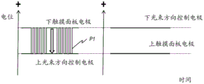
Fig. 9 is a diagram schematically showing waveforms of driving signals supplied to each electrode in a wide viewing angle state. For example, the upper touch panel electrode 12 and the upper beam direction control electrode 18 are applied with a constant reference potential (such as a ground potential). The lower beam direction control electrode 16 is applied with a constant potential higher than the reference potential.
For example, the lower touch panel electrode 13 is applied with a rectangular wave touch panel drive signal having a pulse P1 in a negative direction with respect to the potential supplied to the lower beam direction control electrode 16. The average potential of the rectangular wave is higher than the reference potential. During the period in which the pulse is output, the upper beam direction control electrode 18 may be in a floating state (floating state) so that the electric field is more easily concentrated on the upper beam direction control electrode 18.
In the example of fig. 9, the lower beam direction control electrode 16 is maintained at a higher potential than the upper touch panel electrode 12 facing the lower beam direction control electrode 16, and the lower touch panel electrode 13 is maintained at a higher potential than the upper beam direction control electrode 18 facing the lower touch panel electrode 13. In this way, the electrophoretic particles of the electrophoretic element 14 are concentrated on the lower electrode 7, and a wide viewing angle state can be achieved.
When the pulse P1 is ON (ON) (when a pulse in the negative direction is output), the potential of the lower touch panel electrode 13 is the same as the potential of the upper beam direction control electrode 18 facing the lower touch panel electrode 13, and therefore, if the pulse width is large, the electrophoretic particles can be dispersed therebetween. Therefore, in order to maintain the wide viewing angle state, the pulse width of the pulse P1 must be made sufficiently small so that the electrophoretic particles cannot follow. Specifically, for example, the pulse width is 1 μs to 30 μs. (pulse P1 is provided to charge the electrostatic capacitance, but the charging time is determined by the resistance of the sensor pattern and the resistance of the wiring, the respective capacitances, and the driving voltage. The pulse width used mainly is several microseconds (e.g., 1 μs to 3 μs)).
That is, the duty ratio of the pulse on state (output state) in the entire rectangular wave is equal to or smaller than a predetermined value (the pulse width of P1 is set to be sufficiently shorter than the time (several seconds) for driving the electrophoretic element 14, for example, the duty ratio is 1% or smaller), and the output of the touch panel pulse is terminated before the electrophoretic particles move to the extent that the viewing angle mode changes.
Fig. 10A shows an example of waveforms of driving potentials (driving signals) supplied to the lower electrode 7 in the mutual capacitance mode and the wide viewing angle mode. Fig. 10B shows an example of waveforms of driving potentials (driving signals) supplied to the upper electrode 6 in the mutual capacitance mode and the wide viewing angle mode.
Hereinafter, the lower touch panel electrode 13 is also referred to as an x_1 electrode, an x_2 electrode, and an x_3 electrode … in this order from the positive Y-axis direction, and the lower beam direction control electrode 16 is also referred to as an x2_1 electrode, an x2_2 electrode, and an x2_3 electrode in this order from the positive Y-axis direction. Likewise, the upper touch panel electrode 12 is also referred to as a y_1 electrode, a y_2 electrode, and a y_3 electrode in this order from the negative X-axis direction, and the upper beam direction control electrode 18 is also referred to as a y2_1 electrode, a y2_2 electrode, and a y2_3 electrode in this order from the negative X-axis direction.
After receiving the notification of the mutual capacitance mode from the main controller 21 and the notification of the wide view mode from the view controller 24, the timing controller 25 sequentially selects the lower touch panel electrode 13. The timing controller 25 measures the capacitance of each upper touch panel electrode 12 while supplying a driving potential to the selected lower touch panel electrode 13. The timing controller 25 may measure the capacitance of the lower touch panel electrode 12 by sequentially selecting one by one, or the capacitance between all the upper touch panel electrodes 12 and the selected lower touch panel electrode 13. The touch coordinate calculator 23 calculates touch coordinates based on the measured capacitances.
In the example of fig. 10A, the timing controller 25 selects the lower touch panel electrode 13 in the order of the x_1 electrode, the x_2 electrode, and the x_3 electrode. As shown in fig. 10A, an AC signal is sequentially supplied to the selected lower touch panel electrode 13 to perform capacitance measurement. In the example of fig. 10A, the driving signal supplied to the lower touch panel electrode 13 is a rectangular wave that emits a pulse in the negative direction from a prescribed high potential ("high" in fig. 10A).
The pulses are output in the same order as the selected electrodes, and the pulse output periods of each lower touch panel electrode 13 do not overlap with each other. Moreover, as described above, the pulse width is too short to allow the electrophoretic particles to follow. The driving potential waveform for capacitance measurement may be of any shape as long as it is suitable for touch detection of the beam direction control touch panel 1.
The y_1 electrode, the y_2 electrode, and the y_3 electrode as the upper touch panel electrode 12 are supplied with a constant low potential ("low" in fig. 10B). The x2_1 electrode, the x2_2 electrode, and the x2_3 electrode as the lower beam direction control electrode 16 are supplied with a constant high potential ("high" in fig. 10A), and the y2_1 electrode, the y2_2 electrode, and the y2_3 electrode as the upper beam direction control electrode 18 are supplied with a constant low potential ("low" in fig. 10B).
In this way, as described above, the lower beam direction control electrode 16 is maintained at a higher potential than the upper touch panel electrode 12 facing the lower beam direction control electrode 16, and the lower touch panel electrode 13 is maintained at a higher potential than the upper beam direction control electrode 18 facing the lower touch panel electrode 13. In this way, the electrophoretic particles of the electrophoretic element 14 are concentrated on the lower electrode 7, and a wide viewing angle state can be achieved.
Fig. 11A shows an example of waveforms of driving potentials (driving signals) supplied to the lower electrode 7 in the self-capacitance mode and the wide viewing angle mode. Fig. 11B shows an example of waveforms of driving potentials (driving signals) supplied to the upper electrode 6 in the self-capacitance mode and the wide viewing angle mode.
After receiving the notification of the self-capacitance mode from the main controller 21 and the notification of the wide view mode from the view controller 24, the timing controller 25 measures the capacitances of all the upper touch panel electrodes 12 and all the lower touch panel electrodes 13 while supplying the driving potentials to all the upper touch panel electrodes 12 and all the lower touch panel electrodes 13. Alternatively, the timing controller 25 may be configured to sequentially select each of the upper touch panel electrodes 12 and each of the lower touch panel electrodes 13, and supply a driving signal to the selected electrodes to measure capacitance. The touch coordinate calculator 23 calculates touch coordinates based on the measured capacitances.
In the example of fig. 11A, an AC signal is supplied to the lower touch panel electrode 13 and the lower beam direction control electrode 16 at the same time. In the example of fig. 11A, the driving signal supplied to each lower touch panel electrode 13 and each lower beam direction control electrode 16 is a rectangular wave that emits a pulse from a prescribed high potential ("high" in fig. 11A) in the negative direction. The driving potential waveform for capacitance measurement may be of any shape as long as it is suitable for touch detection of the beam direction control touch panel 1.
The driving signal supplied to each upper touch panel electrode 12 and each upper beam direction control electrode 18 is a rectangular wave that emits a pulse in the negative direction from a prescribed low potential ("low" in fig. 11B). The rectangular wave has the same shape as the rectangular wave represented by the drive signals supplied to the lower touch panel electrode 13 and the lower beam direction control electrode 16. That is, in those rectangular waves, the pulse height, pulse width, and timing of pulse rise are all the same.
In the self-capacitance mode, all the electrodes are supplied with rectangular waves of the same shape, and therefore, the potential difference between the respective electrodes facing each other does not change in the periods of outputting pulses and not outputting pulses. This allows the pulse width to be longer than that of the mutual capacitance mode (for example, as in the mutual capacitance mode, the pulse width is set to about 1 to 30 μs, but the pulse width may be longer than that of the mutual capacitance mode).
In this way, as described above, the lower beam direction control electrode 16 is maintained at a higher potential than the upper touch panel electrode 12 facing the lower beam direction control electrode 16, and the lower touch panel electrode 13 is maintained at a higher potential than the upper beam direction control electrode 18 facing the lower touch panel electrode 13. In this way, the electrophoretic particles of the electrophoretic element 14 are concentrated on the lower electrode 7, and a wide viewing angle state can be achieved.
Fig. 12 is a cross-sectional view showing an example of a cross-sectional structure of the light beam direction control touch panel 1 in a narrow view angle state. For convenience of explanation, in the example of fig. 12, the lower surface (XY plane) of the upper electrode 6 and the upper surface (XY plane) of the lower electrode 7 are drawn on the XZ plane, and the upper transparent substrate 11 and the lower transparent substrate 17 are not shown.
Fig. 13 is a diagram schematically showing waveforms of driving signals supplied to each electrode in a narrow viewing angle state. For example, the upper touch panel electrode 12, the lower beam direction control electrode 16, and the upper beam direction control electrode 18 are applied with a constant reference potential (such as a ground potential). For example, the lower touch panel electrode 13 is applied with a rectangular wave touch panel drive signal having a pulse P2 in a positive direction with respect to a constant reference potential.
When the pulse P2 is ON (output state), the potential of the lower touch panel electrode 13 is higher than the potential of the upper beam direction control electrode 18 facing the lower touch panel electrode 13, and thus, if the pulse width is large, the electrophoretic particles can be concentrated ON the lower touch panel electrode 13. Therefore, in order to maintain the narrow viewing angle state, the pulse width needs to be made sufficiently short so that the electrophoretic particles cannot follow.
Specifically, for example, the pulse width is 1 μs to 30 μs. That is, the duty ratio of the pulse OFF state of the entire rectangular wave (when the reference low potential is maintained) is set to a high level, and the output of the pulse for the touch panel ends before the electrophoretic particles move to a degree that affects the viewing angle mode.
As described above, the lower beam direction control electrode 16 is maintained at the same potential as the upper touch panel electrode 12 facing the lower beam direction control electrode 16, and the lower touch panel electrode 13 is maintained at the same potential as the upper beam direction control electrode 18 facing the lower touch panel electrode 13. In this way, the electrophoretic particles of the electrophoretic element 14 are substantially uniformly dispersed in the dispersion medium, and a narrow viewing angle state can be achieved.
As shown in fig. 12, in this state, if the object touches the upper transparent substrate 11, a part of the electric field formed from the lower touch panel electrode 13 to the upper touch panel electrode 12 through the opening 181 of the upper beam direction control electrode 18 is carried away by the object, which causes a change in capacitance. This makes touch panel functions viable.
Fig. 14A shows an example of waveforms of driving potentials (driving signals) supplied to the lower electrode 7 in the mutual capacitance mode and the narrow viewing angle mode. Fig. 14B shows an example of waveforms of driving potentials (driving signals) supplied to the upper electrode 6 in the mutual capacitance mode and the narrow viewing angle mode.
After receiving the notification of the mutual capacitance mode from the main controller 21 and the notification of the narrow view mode from the view controller 24, the timing controller 25 sequentially selects the lower touch panel electrode 13. The timing controller 25 measures the capacitance of each upper touch panel electrode 12 while supplying a driving potential to the selected lower touch panel electrode 13. The timing controller 25 may measure the capacitance of the upper touch panel electrodes 12 by sequentially selecting one by one, or the capacitance between all the upper touch panel electrodes 12 and the selected lower touch panel electrode 13. The touch coordinate calculator 23 calculates touch coordinates based on the measured capacitances.
In the example of fig. 14A, the timing controller 25 selects the lower touch panel electrode 13 in the order of the x_1 electrode, the x_2 electrode, and the x_3 electrode. As shown in fig. 14A, an AC signal is sequentially supplied to the selected lower touch panel electrode 13 to perform capacitance measurement. In the example of fig. 14A, the driving signal supplied to the lower touch panel electrode 13 is a rectangular wave that emits a pulse in the positive direction from a prescribed low potential ("low" in fig. 14A).
The pulses are output in the same order as the selected electrodes, and the pulse output periods of the respective lower touch panel electrodes 13 do not overlap with each other. Moreover, as described above, the pulse width is too short to allow the electrophoretic particles to follow. The driving potential waveform for capacitance measurement may be of any shape as long as it is suitable for touch detection of the beam direction control touch panel 1.
The y_1 electrode, the y_2 electrode, and the y_3 electrode as the upper touch panel electrode 12, the x2_1 electrode, the x2_2 electrode, and the x2_3 electrode as the lower beam direction control electrode 16, and the y2_1 electrode, the y2_2 electrode, and the y2_3 electrode as the upper beam direction control electrode 18 are supplied with constant low potentials ("low" in fig. 14A and 14B).
Thus, as described above, the lower beam direction control electrode 16 is maintained at the same potential as the upper touch panel electrode 12 facing the lower beam direction control electrode 16, and the lower touch panel electrode 13 is maintained at the same potential as the upper beam direction control electrode 18 facing the lower touch panel electrode 13. In this way, the electrophoretic ions of the electrophoretic element 14 are substantially uniformly dispersed in the dispersion medium, and a narrow viewing angle state can be achieved.
Fig. 15A shows an example of waveforms of driving potentials (driving signals) supplied to the lower electrode 7 in the self-capacitance mode and the narrow viewing angle mode. Fig. 15B shows an example of waveforms of driving potentials (driving signals) supplied to the upper electrode 6 in the self-capacitance mode and the wide viewing angle mode.
After receiving the notification of the self-capacitance mode from the main controller 21 and the notification of the narrow view mode from the view controller 24, the timing controller 25 measures the capacitances of all the upper touch panel electrodes 12 and all the lower touch panel electrodes 13 while supplying the driving potentials to all the upper touch panel electrodes 12 and all the lower touch panel electrodes 13. Alternatively, the timing controller 25 may be configured to sequentially select each of the upper touch panel electrodes 12 and each of the lower touch panel electrodes 13, and supply a driving signal to the selected electrodes to measure capacitance. The touch coordinate calculator 23 calculates touch coordinates based on the measured capacitances.
In the example shown in fig. 15A and 15B, the lower touch panel electrode 13, the lower beam direction control electrode 16, the upper touch panel electrode 12, and the upper beam direction control electrode 18 are simultaneously supplied with AC signals. In the example of fig. 15A and 15B, the driving signals supplied to each lower touch panel electrode 13, each lower beam direction control electrode 16, each upper touch panel electrode 12, and each upper beam direction control electrode 18 are rectangular waves that emit pulses from a prescribed low potential ("low" in fig. 15A) toward the positive direction. The driving potential waveform for capacitance measurement may be of any shape as long as it is suitable for touch detection of the beam direction control touch panel 1.
In the self-capacitance mode, all the electrodes are supplied with rectangular waves of the same shape, and therefore, the potential difference between the electrodes facing each other does not change in the periods of outputting pulses and not outputting pulses. This allows the pulse width to be longer than that of the mutual capacitance mode (for example, as in the mutual capacitance mode, the pulse width is set to about 1 to 30 μs, but the pulse width may be longer than that of the mutual capacitance mode).
Thus, as described above, the lower beam direction control electrode 16 is maintained at the same potential as the upper touch panel electrode 12 facing the lower beam direction control electrode 16, and the lower touch panel electrode 13 is maintained at the same potential as the upper beam direction control electrode 18 facing the lower touch panel electrode 13. In this way, the electrophoretic particles of the electrophoretic element 14 are substantially uniformly dispersed in the dispersion medium, and a narrow viewing angle state can be achieved.
As described above, in the light flux direction control touch panel 1 of the present embodiment, the projected capacitive touch panel and the viewing angle control device capable of electrically controlling the viewing angle are integrally formed and share the same substrate. In this way, a beam direction control touch panel having a multi-touch function can be realized. Also, since the thickness of the beam direction control touch panel 1 is reduced, the distance between the touch portion and the display panel 5 can be smaller. This reduces the difference between the display viewed through the touch panel and the actual display on the display panel, which improves the usability of the panel. Since there are fewer interfaces in the beam direction control touch panel 1, a decrease in transmittance is suppressed, and visibility is improved.
The X electrode and the Y electrode of the touch panel function are disposed on the upper electrode 6 and the lower electrode 7, respectively (or in other words, the two electrodes are disposed on different planes), and thus, it is not necessary to form a bridge (bridge) between the X electrode and the Y electrode. This makes it possible to reduce the number of manufacturing steps, and as a result, the manufacturing cost can be reduced.
Since the lower electrode 7 is disposed on the lower transparent substrate 17, noise from the display panel 5 to the upper transparent substrate 11 can be reduced.
The beam direction control touch panel 1 of the present embodiment is different from embodiment 1 in the driving method in the wide viewing angle mode. The driving method in the narrow viewing angle mode is the same as that of embodiment 1.
Fig. 16 is a diagram schematically showing waveforms of driving signals supplied to each electrode in a wide viewing angle state. For example, embodiment 2 differs from embodiment 1 in that: the lower touch panel electrode 13 is applied with a rectangular wave touch panel drive signal having a pulse P3 in a positive direction with respect to the potential supplied to the lower beam direction control electrode 16.
Even when the pulse P3 is in the ON (condition in which the pulse is being output), the lower touch panel electrode 13 is maintained at a higher potential than the upper beam direction control electrode 18 facing the lower touch panel electrode 13. Accordingly, the pulse width in the wide viewing angle mode of this embodiment may be larger than that of the mutual capacitance mode of embodiment 1 (for example, the pulse width is 1 μs to 30 μs).
Fig. 17 shows an example of waveforms of driving potentials (driving signals) supplied to the lower electrode 7 in the mutual capacitance mode and the wide viewing angle mode. After receiving the notification of the mutual capacitance mode from the main controller 21 and the notification of the wide view mode from the view controller 24, the timing controller 25 sequentially selects the lower touch panel electrode 13.
The timing controller 25 measures the capacitance of each upper touch panel electrode 12 while supplying a driving potential to the selected lower touch panel electrode 13. The timing controller 25 may measure the capacitance of the upper touch panel electrodes 12 by sequentially selecting one by one, or measure the capacitance between all the upper touch panel electrodes 12 and the selected lower touch panel electrode 13. The touch coordinate calculator 23 calculates touch coordinates based on the measured capacitances.
In the example of fig. 17, the timing controller 25 selects the lower touch panel electrode 13 in the order of the x_1 electrode, the x_2 electrode, and the x_3 electrode. As shown in fig. 17, AC signals are sequentially supplied to the selected lower touch panel electrodes 13 to perform capacitance measurement. In the example of fig. 17, the driving signal supplied to the lower touch panel electrode 13 is a rectangular wave that emits a pulse in the positive direction from a prescribed high potential ("high" in fig. 17). The pulses are output in the same order as the selected electrodes, and the pulse output periods of the respective lower touch panel electrodes 13 do not overlap with each other. The driving potential waveform for capacitance measurement may be of any shape as long as it is suitable for touch detection of the beam direction control touch panel 1.
In the mutual capacitance mode and the wide viewing angle state of the present embodiment, the waveform of the driving potential (driving signal) supplied to the upper electrode 6 is the same as that of fig. 10B of embodiment 1, and thus is not shown in the figure.
In this way, as described above, the lower beam direction control electrode 16 is maintained at a higher potential than the upper touch panel electrode 12 facing the lower beam direction control electrode 16, and the lower touch panel electrode 13 is maintained at a higher potential than the upper beam direction control electrode 18 facing the lower touch panel electrode 13. In this way, the electrophoretic particles of the electrophoretic element 14 are concentrated on the lower electrode 7, and a wide viewing angle state can be achieved.
Fig. 18A shows an example of waveforms of driving potentials (driving signals) supplied to the lower electrode 7 in the self-capacitance mode and the wide viewing angle mode. Fig. 18B shows an example of waveforms of driving potentials (driving signals) supplied to the upper electrode 6 in the self-capacitance mode and the wide viewing angle mode.
After receiving the notification of the self-capacitance mode from the main controller 21 and the notification of the wide view mode from the view controller 24, the timing controller 25 measures the capacitances of all the upper touch panel electrodes 12 and all the lower touch panel electrodes 13 while supplying the driving potentials to all the upper touch panel electrodes 12 and all the lower touch panel electrodes 13. Alternatively, the timing controller 25 may be configured to sequentially select each of the upper touch panel electrodes 12 and each of the lower touch panel electrodes 13, and supply a driving signal to the selected electrodes to measure capacitance. The touch coordinate calculator 23 calculates touch coordinates based on the measured capacitances.
In the example of fig. 18A, an AC signal is supplied to the lower touch panel electrode 13 and the lower beam direction control electrode 16 at the same time. In the example of fig. 18A, the driving signal supplied to each lower touch panel electrode 13 and each lower beam direction control electrode 16 is a rectangular wave that emits a pulse in the positive direction from a prescribed high potential ("high" in fig. 18A). The driving potential waveform for capacitance measurement may be of any shape as long as it is suitable for touch detection of the beam direction control touch panel 1.
The driving signal supplied to each upper touch panel electrode 12 and each upper beam direction control electrode 18 is a rectangular wave that emits a pulse in the positive direction from a prescribed low potential ("low" in fig. 18B). The rectangular wave has the same shape as the rectangular wave represented by the drive signals supplied to the lower touch panel electrode 13 and the lower beam direction control electrode 16.
In this way, as described above, the lower beam direction control electrode 16 is maintained at a higher potential than the upper touch panel electrode 12 facing the lower beam direction control electrode 16, and the lower touch panel electrode 13 is maintained at a higher potential than the upper beam direction control electrode 18 facing the lower touch panel electrode 13. In this way, the electrophoretic particles of the electrophoretic element 14 are concentrated on the lower electrode 7, and a wide viewing angle state can be achieved.
In the mutual capacitance mode of the present embodiment, the electric field size of the touch panel (the potential difference between the lower touch panel electrode 13 and the upper touch panel electrode 12 when a pulse is output) is larger in the wide viewing angle than in the narrow viewing angle mode. That is, between the wide view angle mode and the narrow view angle mode, although the magnitude of the electrostatic capacitance of the touch panel is the same, periods required to charge the electrostatic capacitance are different from each other.
As shown in the following equation 1, as the voltage becomes higher, the period required for the electrostatic capacitance to be charged to the prescribed voltage is longer. Accordingly, the main controller 21 determines the charging time of the electrostatic capacitance and the measurement timing of the electrostatic capacitance so that the charge amount in the wide view mode is the same as in the narrow view mode based on, for example, the following equation 2, and the main controller 21 supplies the information of the charging time and timing to the timing controller 25.
e C (t)=E-E·e -t/RC .. (equation 1) (e C Is the voltage of the capacitor, E is the voltage applied to the electrode, t is the charging time, R is the resistance, and C is the electrostatic capacitance).
q(t)=CE-CE -t/RC .. (equation 2) (q is the voltage of the capacitor, E is the voltage applied to the electrode, t is the charge time, R is the resistance, and C is the electrostatic capacitance).
The beam direction control touch panel 1 of the present embodiment is different from the beam direction control touch panel 1 of embodiment 1 in that: an opening is also formed in the upper touch panel electrode 12. Fig. 19 is a plan view schematically showing a structural example of the upper electrode 6 of the present embodiment. An opening 121 is formed in the upper touch panel electrode 12. In the example of fig. 19, each electrode piece of the upper touch panel electrode 12 has a plurality of openings 121 in a rectangular shape in which the Y-axis direction is the length direction. The shape of the opening 121 is not limited to a rectangular shape, and the opening 121 may be formed in any shape.
Fig. 20 is a sectional view showing an example of a sectional structure of the light beam direction control touch panel 1 in a wide view angle state taken along a line AA' of fig. 19. Fig. 21 is a sectional view showing an example of a sectional structure of the beam direction control touch panel 1 taken along the line BB' of fig. 19. Fig. 22 is a sectional view showing an example of a sectional structure of the beam direction control touch panel 1 taken along the line CC' of fig. 19.
The opening 121 formed in the upper touch panel electrode 12 is formed to overlap in position with the light-transmitting region 15. Preferably, the opening 121 does not overlap the electrophoretic element 14. Therefore, it is preferable that the width (in the X-axis direction) of the opening 121 is smaller than the width of the light-transmitting region 15. All the electrophoretic elements 14 are sandwiched by at least one upper touch panel electrode 12 or at least one upper beam direction control electrode 18 and at least one lower touch panel electrode 13 or at least one lower beam direction control electrode 16.
Fig. 23 is a sectional view showing an example of a sectional structure of the light flux direction control touch panel 1 in a wide view angle state. For convenience of explanation, in the example of fig. 23, the lower surface (XY plane) of the upper electrode 6 and the upper surface (XY plane) of the lower electrode 7 are drawn on the XZ plane, and the upper transparent substrate 11 and the lower transparent substrate 17 are not shown.
In fig. 23, the lower touch panel electrode 13 is controlled to have a higher potential than the upper beam direction control electrode 18 facing the lower touch panel electrode 13. The lower beam direction control electrode 16 is controlled to have a higher potential than the upper touch panel electrode 12 facing the lower beam direction control electrode 16. In this way, an electric field is formed from the lower touch panel electrode 13 to the non-opening area of the upper beam direction control electrode 18, and an electric field is formed from the lower beam direction control electrode 16 to the upper touch panel electrode 12, thereby realizing a beam direction control function.
In this state, if the object touches the upper transparent substrate 11, a part of the electric field formed from the lower touch panel electrode 13 to the upper touch panel electrode 12 through the opening 181 of the upper beam direction control electrode 18 is carried away by the object, which causes a change in capacitance. In addition, a part of the electric field formed from the lower beam direction control electrode 16 to the upper beam direction control electrode 18 through the opening 121 of the upper touch panel electrode 12 is carried away by the object, which causes a change in capacitance. The touch panel functions are enabled by these electric fields.
That is, in the beam direction control touch panel 1 of the present embodiment, not only the upper touch panel electrode 12 and the lower touch panel electrode 13, but also the upper beam direction control electrode 18 and the lower beam direction control electrode 16 function as both the touch panel electrode and the beam direction control electrode. This improves the resolution of the touch panel.
Specifically, in the present embodiment, in the mutual capacitance mode, both the lower touch panel electrode 13 and the lower beam direction control electrode 16 function as transmitting electrodes (driving electrodes), and both the upper touch panel electrode 12 and the upper beam direction control electrode 18 function as receiving electrodes (driving electrodes).
Therefore, in this embodiment, in the mutual capacitance mode, the timing controller 25 sequentially selects each lower touch panel electrode 13 and each lower beam direction control electrode 16. The timing controller 25 measures the capacitance of each of the upper touch panel electrode 12 and the upper beam direction control electrode 18, while the timing controller 25 supplies the drive potential to the selected lower touch panel electrode 13 and lower beam direction control electrode 16.
In the mutual capacitance mode, the timing controller 25 may measure capacitance by sequentially selecting each upper touch panel electrode 12 and each upper beam direction control electrode 18, or measure capacitance between all upper touch panel electrodes 12 and upper beam direction control electrodes 18 and the selected lower touch panel electrodes 13 and the selected lower beam direction control electrodes 16. The touch coordinate calculator 23 calculates touch coordinates based on the measured capacitances.
In the mutual capacitance mode, both the lower touch panel electrode 13 and the lower beam direction control electrode 16 can be used as emission electrodes by sequentially supplying pulses sequentially supplied to the x_1 electrode, the x_2 electrode, and the x_3 electrode in embodiment 1 and embodiment 2 (fig. 10A, 14A, and 17) to the x_1, the x2_1, the x_2, the x2_2, the x_3, and the x2_3 electrodes. The drive potential supplied to the upper touch panel electrode 12 and the upper beam direction control electrode 18 is the same as that of embodiment 1.
In the self-capacitance mode, both the lower touch panel electrode 13 and the lower beam direction control electrode 16 function as X electrodes, and both the upper touch panel electrode 12 and the upper beam direction control electrode 18 function as Y electrodes.
In the self-capacitance mode, the timing controller 25 measures the capacitances of all the upper touch panel electrodes 12 and all the upper beam direction control electrodes 18 and all the lower touch panel electrodes 13 and all the lower beam direction control electrodes 16, while supplying driving potentials to all the upper touch panel electrodes 12 and all the upper beam direction control electrodes 18 and all the lower touch panel electrodes 13 and all the lower beam direction control electrodes 16.
Alternatively, the timing controller 25 may be configured to sequentially select each of the upper touch panel electrode 12, the upper beam control electrode 18, the lower touch panel electrode 13, and the lower beam direction control electrode 16, and supply a driving signal to the selected electrode to measure the capacitance thereof. The touch coordinate calculator 23 calculates touch coordinates based on the measured capacitances. The driving potential supplied to each electrode in the self-capacitance mode is the same as that of embodiment mode 1 and embodiment mode 2.
In the present embodiment, the upper touch panel electrode 12 and the upper beam direction control electrode 18 may be regarded as the same, and therefore, the upper touch panel electrode driver 26 and the upper beam direction control electrode driver 27 may be integrally formed as one functional portion. Also, the lower touch panel electrode 13 and the lower beam direction control electrode 16 may be regarded as the same, and therefore, the lower touch panel electrode driver 28 and the lower beam direction control electrode driver 29 may be integrally formed as one functional part.
Embodiment 4
The beam direction control touch panel 1 of the present embodiment is different from embodiment 1 in the arrangement and shape of electrodes in the upper electrode 6 and the lower electrode 7.
Fig. 24 is a plan view schematically showing a structural example of the upper electrode 6 of the present embodiment. The upper electrode 6 includes a plurality of upper touch panel electrodes 12 and a plurality of upper beam direction control electrodes 18. The plurality of upper touch panel electrodes 12 each extend in the Y-axis direction and are arranged at regular intervals in the X-axis direction. For example, each upper touch panel electrode 12 has a rectangular shape in which the Y-axis direction is the length direction.
The plurality of upper beam direction control electrodes 18 each extend in the Y-axis direction and are arranged at intervals in the X-axis direction. For example, each upper beam direction control electrode 18 has a rectangular shape in which the Y-axis direction is the length direction. At least one opening 181 is formed in the upper beam direction control electrode 18. For example, the opening 181 has a rectangular shape in which the Y-axis direction is the longitudinal direction.
The upper touch panel electrodes 12 and the upper beam direction control electrodes 18 are alternately arranged in the X-axis direction. The gap between the upper beam direction control electrode 18 and the upper touch panel electrode 12 may be filled with an insulating material (e.g., silicon nitride), or remain unfilled.
Fig. 25 is a plan view schematically showing a structural example of the lower electrode 7 of the present embodiment. The lower electrode 7 includes a plurality of lower touch panel electrodes 13. The plurality of lower touch panel electrodes 13 extend in the X-axis direction on the lower transparent substrate 17, respectively, and are arranged at regular intervals in the Y-axis direction. Each of the lower touch panel electrodes 13 has a rectangular shape in which the X-axis direction is the length direction. For example, the gaps between the respective lower touch panel electrodes 13 may be filled with an insulating material (such as silicon nitride), or remain unfilled.
Fig. 26 is a sectional view showing an example of a sectional structure of the light beam direction control touch panel 1 in a wide view angle state taken along the line AA' of fig. 24 and 25. Fig. 27 is a sectional view showing an example of a sectional structure of the light beam direction control touch panel 1 in a wide view angle state taken along a line BB' of fig. 24 and 25.
The opening 181 formed in the upper beam direction control electrode 18 is formed to overlap in position with the light transmitting region 15. Preferably, the opening 181 does not overlap the electrophoretic element 14. Therefore, it is preferable that the width (in the X-axis direction) of the opening 181 is smaller than the width of the light transmitting region 15.
All the electrophoretic elements 14 are sandwiched by at least one upper touch panel electrode 12 or at least one upper beam direction control electrode 18 and at least one lower touch panel electrode 13. The electrophoresis element 14 is perpendicular to the lower touch panel electrode 13 on the XY plane.
As shown in fig. 27, the lower touch panel electrode 13 is controlled to have a higher potential than the upper beam direction control electrode 18 and the upper touch panel electrode 12 facing the lower touch panel electrode 13. In this way, an electric field is formed from the lower touch panel 13 to the non-opening area of the upper beam direction control electrode 18, and an electric field is formed from the lower touch panel electrode 13 to the upper touch panel electrode 12, thereby realizing the beam direction control function.
In this state, if the object touches the upper transparent substrate 11, an electric field is formed from the lower touch panel electrode 13 to the upper touch panel electrode 12 via the opening 181 of the upper beam direction control electrode 18. The touch panel function is enabled by the electric field. The driving potential supplied to each electrode in the self-capacitance mode is the same as that of embodiment mode 1 and embodiment mode 2, and the description thereof will not be repeated.
Similar to the embodiment shown in fig. 19, in the beam direction control touch panel 1 of the present embodiment, an opening may be formed in the upper touch panel electrode 12. In this way, not only the upper beam direction control electrode 18 and the lower touch panel electrode 13, but also the upper touch panel electrode 12 and the lower touch panel electrode 13 function as both the touch panel electrode and the beam direction control electrode. This improves the resolution of the touch panel.
The embodiments of the present invention have been described above, but the present invention is not limited to these embodiments. Each of the elements of the above-described embodiments may be readily modified, added or changed by those skilled in the art without departing from the scope of the present invention. A portion of the structure of one embodiment may be replaced with the structure of another embodiment, or the structure of one embodiment may be added to the structure of another embodiment.
Claims (10)
1. A beam direction control touch panel device comprising:
an upper transparent substrate;
a lower transparent substrate;
a plurality of upper beam direction control electrodes and a plurality of upper touch panel electrodes alternately disposed on a lower surface of the upper transparent substrate along a first direction;
a plurality of lower touch panel electrodes disposed on an upper surface of the lower transparent substrate and facing the upper beam direction control electrodes;
a plurality of electrophoretic elements interposed between the plurality of upper beam direction control electrodes and the plurality of lower touch panel electrodes, each of the plurality of electrophoretic elements including colored electrophoretic particles and a dispersion medium;
A plurality of light-transmitting regions interposed between the upper transparent substrate and the lower transparent substrate, the plurality of light-transmitting regions being surrounded by the electrophoretic element; and
the controller is used for controlling the operation of the controller,
wherein the plurality of upper beam direction control electrodes respectively comprise openings overlapped with the light transmission area in position,
wherein the controller is configured to:
providing a driving potential to the plurality of lower touch panel electrodes in capacitance measurement for detecting touch positions, thereby forming electric fields from the plurality of lower touch panel electrodes to the plurality of upper touch panel electrodes via the openings; and
and providing a driving potential to the plurality of upper beam direction control electrodes according to the driving potential provided to the plurality of lower touch panel electrodes, thereby switching between a dispersed state and a concentrated state of the colored electrophoretic particles in the plurality of electrophoretic elements.
2. The beam direction control touch panel device according to claim 1,
wherein the controller is configured to: in the wide viewing angle mode of operation,
maintaining the colored electrophoretic particles in the plurality of electrophoretic elements in the concentrated state; and is also provided with
And supplying a potential to the plurality of upper beam direction control electrodes, the potential having a constant difference from a driving potential supplied to the plurality of lower touch panel electrodes.
3. The beam direction control touch panel device according to claim 1,
wherein the controller is configured to: in the mode of the narrow viewing angle,
maintaining the colored electrophoretic particles in the plurality of electrophoretic elements in the dispersed state; and is also provided with
The same electric potential is supplied to the plurality of upper beam direction control electrodes and the plurality of lower touch panel electrodes.
4. The beam direction control touch panel device according to claim 1, wherein the opening does not overlap with the electrophoresis element in position.
5. The beam direction control touch panel device according to claim 1, wherein the controller supplies a driving potential to the plurality of lower touch panel electrodes, the driving potential being represented by a rectangular wave including a pulse from a reference potential, and
wherein the pulse width of the pulse is too small to allow the electrophoretic particles of the electrophoretic element to follow.
6. The beam direction control touch panel device according to claim 1,
wherein the controller is configured to:
in the wide viewing angle mode of operation,
maintaining the colored electrophoretic particles in the plurality of electrophoretic elements in the concentrated state; and supplying a potential to the plurality of upper beam direction control electrodes, the potential having a constant difference from a driving potential supplied to the plurality of lower touch panel electrodes, an
In the mode of the narrow viewing angle,
maintaining the colored electrophoretic particles in the plurality of electrophoretic elements in the dispersed state; and the same electric potential is supplied to the plurality of upper beam direction control electrodes and the plurality of lower touch panel electrodes,
wherein when capacitances of the plurality of lower touch panel electrodes are being charged, potential differences between the plurality of lower touch panel electrodes and the plurality of upper touch panel electrodes are different in the wide view angle mode and the narrow view angle mode, and
wherein the controller determines a capacitance charging time such that an amount of charge in the plurality of lower touch panel electrodes is the same in the wide view angle mode and the narrow view angle mode.
7. The beam direction control touch panel device according to claim 1, further comprising: a plurality of lower beam direction control electrodes disposed on an upper surface of the lower transparent substrate such that the lower beam direction control electrodes and the lower touch panel electrodes are alternately disposed along a second direction perpendicular to the first direction, the plurality of lower beam direction control electrodes facing the upper touch panel electrodes,
Wherein the plurality of electrophoretic elements are sandwiched by the plurality of upper touch panel electrodes and the plurality of lower beam direction control electrodes, and
wherein the controller is configured to supply a driving potential to the plurality of lower beam direction control electrodes in accordance with the driving potential supplied to the plurality of upper touch panel electrodes, thereby switching between a dispersed state and a concentrated state of the colored electrophoretic particles in the plurality of electrophoretic elements.
8. The beam direction control touch panel device according to claim 7, wherein the plurality of upper touch panel electrodes respectively include openings that positionally overlap the light-transmitting region, and
wherein driving potentials are supplied to the plurality of lower beam direction control electrodes in capacitance measurement for detecting touch positions, thereby forming electric fields from the plurality of lower beam direction control electrodes to the plurality of upper beam direction control electrodes via the openings of the plurality of upper touch panel electrodes.
9. The beam direction control touch panel device according to claim 7, wherein the plurality of electrophoretic elements extend in the second direction and are arranged in the first direction,
Wherein the plurality of lower touch panel electrodes, the plurality of lower beam direction control electrodes, the plurality of upper touch panel electrodes, and the plurality of upper beam direction control electrodes have a structure in which a plurality of electrode sheets are connected to each other, respectively,
wherein each electrode piece of the plurality of lower touch panel electrodes faces one of electrode pieces of the plurality of upper beam direction control electrodes,
wherein each electrode piece of the plurality of lower beam direction control electrodes faces one of the electrode pieces of the plurality of upper touch panel electrodes,
wherein the plurality of lower touch panel electrodes and the plurality of lower beam direction control electrodes extend in the first direction and are arranged in the second direction, and
wherein the plurality of upper touch panel electrodes and the plurality of upper beam direction control electrodes extend in the second direction and are arranged in the first direction.
10. The beam direction control touch panel device according to claim 1,
wherein the plurality of electrophoretic elements extend in a second direction perpendicular to the first direction and are arranged in the first direction,
wherein the plurality of lower touch panel electrodes, the plurality of upper touch panel electrodes, and the plurality of upper beam direction control electrodes have rectangular shapes, respectively,
Wherein the plurality of lower touch panel electrodes extend in the first direction and are arranged in the second direction, and
wherein the plurality of upper touch panel electrodes and the plurality of upper beam direction control electrodes extend in the second direction and are arranged in the first direction.
Applications Claiming Priority (2)
| Application Number | Priority Date | Filing Date | Title |
|---|---|---|---|
| JP2017-225028 | 2017-11-22 | ||
| JP2017225028A JP6966033B2 (en) | 2017-11-22 | 2017-11-22 | Ray direction control touch panel device |
Publications (2)
| Publication Number | Publication Date |
|---|---|
| CN110045883A CN110045883A (en) | 2019-07-23 |
| CN110045883B true CN110045883B (en) | 2023-05-02 |
Family
ID=66534266
Family Applications (1)
| Application Number | Title | Priority Date | Filing Date |
|---|---|---|---|
| CN201811346137.7A Active CN110045883B (en) | 2017-11-22 | 2018-11-13 | Light beam direction control touch panel device |
Country Status (3)
| Country | Link |
|---|---|
| US (1) | US10788924B2 (en) |
| JP (1) | JP6966033B2 (en) |
| CN (1) | CN110045883B (en) |
Families Citing this family (1)
| Publication number | Priority date | Publication date | Assignee | Title |
|---|---|---|---|---|
| CN108427219B (en) * | 2018-06-01 | 2020-12-04 | 京东方科技集团股份有限公司 | Display panel, display device and control method thereof |
Citations (2)
| Publication number | Priority date | Publication date | Assignee | Title |
|---|---|---|---|---|
| JP2012256286A (en) * | 2011-06-10 | 2012-12-27 | Seiko Epson Corp | Input device and input system |
| CN105900045A (en) * | 2013-09-27 | 2016-08-24 | 森赛尔股份有限公司 | Touch sensor detector system and method |
Family Cites Families (16)
| Publication number | Priority date | Publication date | Assignee | Title |
|---|---|---|---|---|
| US6184856B1 (en) * | 1998-09-16 | 2001-02-06 | International Business Machines Corporation | Transmissive electrophoretic display with laterally adjacent color cells |
| WO2006030745A1 (en) | 2004-09-17 | 2006-03-23 | Sharp Kabushiki Kaisha | Display, viewing angle controller, and electronic apparatus |
| US20070085837A1 (en) * | 2005-10-17 | 2007-04-19 | Eastman Kodak Company | Touch input device with display front |
| KR101320500B1 (en) * | 2008-11-20 | 2013-10-22 | 엘지디스플레이 주식회사 | Touch type electrophoretic display device |
| JP5332589B2 (en) * | 2008-12-19 | 2013-11-06 | セイコーエプソン株式会社 | Electrophoretic display device driving method, electrophoretic display device, and electronic apparatus |
| US20120146943A1 (en) * | 2009-09-03 | 2012-06-14 | Koninklijke Philips Electronics N.V. | Touch sensing output device |
| KR20120010795A (en) * | 2010-07-27 | 2012-02-06 | 삼성전기주식회사 | Electronic paper associated with touch panel |
| US20120062503A1 (en) * | 2010-09-14 | 2012-03-15 | Motorola-Mobility, Inc. | Device for integrating capactive touch with electrophoretic displays |
| JP6443691B2 (en) * | 2014-02-17 | 2018-12-26 | Tianma Japan株式会社 | OPTICAL ELEMENT AND MANUFACTURING METHOD THEREOF, DISPLAY DEVICE, ELECTRONIC DEVICE, AND LIGHTING DEVICE HAVING OPTICAL ELEMENT |
| JP6185889B2 (en) * | 2014-07-04 | 2017-08-23 | 株式会社ジャパンディスプレイ | Display device and driving method thereof |
| CN105425502B (en) | 2014-09-12 | 2019-11-05 | Nlt科技股份有限公司 | Optical element and the display device using the optical element, electronic equipment, lighting device |
| CN105425501B (en) * | 2014-09-12 | 2019-07-30 | Nlt科技股份有限公司 | Optical element and the display device using the optical element, electronic equipment, lighting device |
| JP6566304B2 (en) | 2014-09-12 | 2019-08-28 | Tianma Japan株式会社 | OPTICAL ELEMENT AND DISPLAY DEVICE, ELECTRONIC DEVICE, AND LIGHTING DEVICE USING THE SAME |
| JP6601660B2 (en) * | 2014-09-12 | 2019-11-06 | Tianma Japan株式会社 | OPTICAL ELEMENT AND DISPLAY DEVICE, ELECTRONIC DEVICE, AND LIGHTING DEVICE USING SAME |
| JP7036312B2 (en) * | 2017-09-29 | 2022-03-15 | 天馬微電子有限公司 | Ray direction control touch panel device and display device |
| JP6966032B2 (en) * | 2017-11-16 | 2021-11-10 | Tianma Japan株式会社 | Ray direction control touch panel device |
-
2017
- 2017-11-22 JP JP2017225028A patent/JP6966033B2/en active Active
-
2018
- 2018-11-13 CN CN201811346137.7A patent/CN110045883B/en active Active
- 2018-11-21 US US16/197,724 patent/US10788924B2/en active Active
Patent Citations (2)
| Publication number | Priority date | Publication date | Assignee | Title |
|---|---|---|---|---|
| JP2012256286A (en) * | 2011-06-10 | 2012-12-27 | Seiko Epson Corp | Input device and input system |
| CN105900045A (en) * | 2013-09-27 | 2016-08-24 | 森赛尔股份有限公司 | Touch sensor detector system and method |
Also Published As
| Publication number | Publication date |
|---|---|
| US10788924B2 (en) | 2020-09-29 |
| JP2019096066A (en) | 2019-06-20 |
| JP6966033B2 (en) | 2021-11-10 |
| US20190155440A1 (en) | 2019-05-23 |
| CN110045883A (en) | 2019-07-23 |
Similar Documents
| Publication | Publication Date | Title |
|---|---|---|
| CN109582172B (en) | Light distribution controllable touch panel device and display device | |
| KR102489827B1 (en) | Display device | |
| US9176586B2 (en) | Touch panel device with tactile sense presenting function | |
| KR101663763B1 (en) | Display device with touch screen | |
| KR101841060B1 (en) | Method of detecting touch position, touch substrate and display device having the same | |
| KR102350084B1 (en) | Touch panel and display device using the same | |
| JP7261097B2 (en) | Beam direction control device and electronic equipment | |
| US11693503B2 (en) | Display device | |
| US10126865B2 (en) | Touch control display panel and display device | |
| US11169643B2 (en) | Touch panel and touch panel device | |
| CN104020899A (en) | Single-layer capacitive touch device and panel module thereof | |
| US20120075235A1 (en) | Method of determining touch coordinate and touch panel assembly for performing the same | |
| CN110045883B (en) | Light beam direction control touch panel device | |
| CN109799931B (en) | Light distribution controllable touch panel device | |
| JP6001764B2 (en) | Touch detection module and contact touch detection method in the touch detection module | |
| US10976861B2 (en) | Detection device and display device | |
| US10691278B1 (en) | Reduced line count touch panel for mutual capacitance measurements | |
| KR20200077987A (en) | Touch screen panel and touch screen integrated display Device | |
| KR101790452B1 (en) | Input device |
Legal Events
| Date | Code | Title | Description |
|---|---|---|---|
| PB01 | Publication | ||
| PB01 | Publication | ||
| SE01 | Entry into force of request for substantive examination | ||
| SE01 | Entry into force of request for substantive examination | ||
| GR01 | Patent grant | ||
| GR01 | Patent grant |