CN110010552B - s-contact for silicon-on-insulator - Google Patents
s-contact for silicon-on-insulator Download PDFInfo
- Publication number
- CN110010552B CN110010552B CN201910222017.4A CN201910222017A CN110010552B CN 110010552 B CN110010552 B CN 110010552B CN 201910222017 A CN201910222017 A CN 201910222017A CN 110010552 B CN110010552 B CN 110010552B
- Authority
- CN
- China
- Prior art keywords
- contact
- conductive
- semiconductor device
- region
- semiconductor substrate
- Prior art date
- Legal status (The legal status is an assumption and is not a legal conclusion. Google has not performed a legal analysis and makes no representation as to the accuracy of the status listed.)
- Active
Links
Images


Classifications
-
- H—ELECTRICITY
- H10—SEMICONDUCTOR DEVICES; ELECTRIC SOLID-STATE DEVICES NOT OTHERWISE PROVIDED FOR
- H10D—INORGANIC ELECTRIC SEMICONDUCTOR DEVICES
- H10D87/00—Integrated devices comprising both bulk components and either SOI or SOS components on the same substrate
-
- H—ELECTRICITY
- H10—SEMICONDUCTOR DEVICES; ELECTRIC SOLID-STATE DEVICES NOT OTHERWISE PROVIDED FOR
- H10D—INORGANIC ELECTRIC SEMICONDUCTOR DEVICES
- H10D84/00—Integrated devices formed in or on semiconductor substrates that comprise only semiconducting layers, e.g. on Si wafers or on GaAs-on-Si wafers
- H10D84/80—Integrated devices formed in or on semiconductor substrates that comprise only semiconducting layers, e.g. on Si wafers or on GaAs-on-Si wafers characterised by the integration of at least one component covered by groups H10D12/00 or H10D30/00, e.g. integration of IGFETs
- H10D84/82—Integrated devices formed in or on semiconductor substrates that comprise only semiconducting layers, e.g. on Si wafers or on GaAs-on-Si wafers characterised by the integration of at least one component covered by groups H10D12/00 or H10D30/00, e.g. integration of IGFETs of only field-effect components
- H10D84/83—Integrated devices formed in or on semiconductor substrates that comprise only semiconducting layers, e.g. on Si wafers or on GaAs-on-Si wafers characterised by the integration of at least one component covered by groups H10D12/00 or H10D30/00, e.g. integration of IGFETs of only field-effect components of only insulated-gate FETs [IGFET]
- H10D84/85—Complementary IGFETs, e.g. CMOS
-
- H—ELECTRICITY
- H10—SEMICONDUCTOR DEVICES; ELECTRIC SOLID-STATE DEVICES NOT OTHERWISE PROVIDED FOR
- H10D—INORGANIC ELECTRIC SEMICONDUCTOR DEVICES
- H10D62/00—Semiconductor bodies, or regions thereof, of devices having potential barriers
- H10D62/10—Shapes, relative sizes or dispositions of the regions of the semiconductor bodies; Shapes of the semiconductor bodies
- H10D62/113—Isolations within a component, i.e. internal isolations
- H10D62/115—Dielectric isolations, e.g. air gaps
-
- H—ELECTRICITY
- H10—SEMICONDUCTOR DEVICES; ELECTRIC SOLID-STATE DEVICES NOT OTHERWISE PROVIDED FOR
- H10D—INORGANIC ELECTRIC SEMICONDUCTOR DEVICES
- H10D64/00—Electrodes of devices having potential barriers
- H10D64/60—Electrodes characterised by their materials
- H10D64/62—Electrodes ohmically coupled to a semiconductor
-
- H—ELECTRICITY
- H10—SEMICONDUCTOR DEVICES; ELECTRIC SOLID-STATE DEVICES NOT OTHERWISE PROVIDED FOR
- H10D—INORGANIC ELECTRIC SEMICONDUCTOR DEVICES
- H10D84/00—Integrated devices formed in or on semiconductor substrates that comprise only semiconducting layers, e.g. on Si wafers or on GaAs-on-Si wafers
- H10D84/01—Manufacture or treatment
- H10D84/0123—Integrating together multiple components covered by H10D12/00 or H10D30/00, e.g. integrating multiple IGBTs
- H10D84/0126—Integrating together multiple components covered by H10D12/00 or H10D30/00, e.g. integrating multiple IGBTs the components including insulated gates, e.g. IGFETs
- H10D84/0149—Manufacturing their interconnections or electrodes, e.g. source or drain electrodes
-
- H—ELECTRICITY
- H10—SEMICONDUCTOR DEVICES; ELECTRIC SOLID-STATE DEVICES NOT OTHERWISE PROVIDED FOR
- H10D—INORGANIC ELECTRIC SEMICONDUCTOR DEVICES
- H10D84/00—Integrated devices formed in or on semiconductor substrates that comprise only semiconducting layers, e.g. on Si wafers or on GaAs-on-Si wafers
- H10D84/01—Manufacture or treatment
- H10D84/0123—Integrating together multiple components covered by H10D12/00 or H10D30/00, e.g. integrating multiple IGBTs
- H10D84/0126—Integrating together multiple components covered by H10D12/00 or H10D30/00, e.g. integrating multiple IGBTs the components including insulated gates, e.g. IGFETs
- H10D84/0151—Manufacturing their isolation regions
-
- H—ELECTRICITY
- H10—SEMICONDUCTOR DEVICES; ELECTRIC SOLID-STATE DEVICES NOT OTHERWISE PROVIDED FOR
- H10D—INORGANIC ELECTRIC SEMICONDUCTOR DEVICES
- H10D84/00—Integrated devices formed in or on semiconductor substrates that comprise only semiconducting layers, e.g. on Si wafers or on GaAs-on-Si wafers
- H10D84/01—Manufacture or treatment
- H10D84/02—Manufacture or treatment characterised by using material-based technologies
- H10D84/03—Manufacture or treatment characterised by using material-based technologies using Group IV technology, e.g. silicon technology or silicon-carbide [SiC] technology
- H10D84/038—Manufacture or treatment characterised by using material-based technologies using Group IV technology, e.g. silicon technology or silicon-carbide [SiC] technology using silicon technology, e.g. SiGe
-
- H—ELECTRICITY
- H10—SEMICONDUCTOR DEVICES; ELECTRIC SOLID-STATE DEVICES NOT OTHERWISE PROVIDED FOR
- H10D—INORGANIC ELECTRIC SEMICONDUCTOR DEVICES
- H10D86/00—Integrated devices formed in or on insulating or conducting substrates, e.g. formed in silicon-on-insulator [SOI] substrates or on stainless steel or glass substrates
- H10D86/01—Manufacture or treatment
-
- H—ELECTRICITY
- H10—SEMICONDUCTOR DEVICES; ELECTRIC SOLID-STATE DEVICES NOT OTHERWISE PROVIDED FOR
- H10D—INORGANIC ELECTRIC SEMICONDUCTOR DEVICES
- H10D86/00—Integrated devices formed in or on insulating or conducting substrates, e.g. formed in silicon-on-insulator [SOI] substrates or on stainless steel or glass substrates
- H10D86/201—Integrated devices formed in or on insulating or conducting substrates, e.g. formed in silicon-on-insulator [SOI] substrates or on stainless steel or glass substrates the substrates comprising an insulating layer on a semiconductor body, e.g. SOI
Landscapes
- Thin Film Transistor (AREA)
Abstract
公开了用于绝缘体上硅的s接触(s‑contact)。描述了用于使用电阻式结构改善防止电荷注入器件层中的系统、方法和装置。可以使用更简单的制造方法和更少的制造步骤来制作这样的电阻式结构,即s接触部。对于金属氧化物半导体(MOS)场效应晶体管(FET),可以将s接触部制作成直接连接或电阻式连接至晶体管的所有区,包括源极区、漏极区和栅极。
An s-contact for silicon-on-insulator is disclosed. Systems, methods, and apparatus are described for improving prevention of charge injection into device layers using resistive structures. Such a resistive structure, ie, the s-contact, can be fabricated using simpler fabrication methods and fewer fabrication steps. For a Metal Oxide Semiconductor (MOS) Field Effect Transistor (FET), the s-contact can be made to connect directly or resistively to all regions of the transistor, including the source, drain and gate.
Description
本申请是申请日为2016年10月10日、申请号为201610885245.6、发明名称为“用于绝缘体上硅的s接触”的发明专利申请的分案申请。This application is a divisional application of an invention patent application with an application date of October 10, 2016, an application number of 201610885245.6, and an invention title of "s-contact for silicon-on-insulator".
技术领域technical field
本文中描述的各实施方式一般涉及用于在器件的制造阶段期间防止绝缘体上硅(SOI)器件充电的系统、方法和设备。Embodiments described herein generally relate to systems, methods, and apparatus for preventing charging of silicon-on-insulator (SOI) devices during stages of fabrication of the devices.
背景技术Background technique
半导体器件的制造阶段可以包括:使半导体器件经受电势梯度或者在半导体器件的表面上感应出电荷的过程。在一些情况下,与这样的过程相关联的高能带电粒子(离子)进而可以进入半导体器件的层中,并且在这样的层内被俘获。层内被俘获的电荷进而会对半导体器件的工作特性产生不利影响,例如相应阈值电压的高变化,并且在极端情况下可以造成器件的内部结构/层的破裂,从而导致器件无功能。The fabrication stages of a semiconductor device may include the process of subjecting the semiconductor device to a potential gradient or inducing charges on the surface of the semiconductor device. In some cases, energetic charged particles (ions) associated with such processes can in turn enter into layers of a semiconductor device and become trapped within such layers. Trapped charges within the layers can in turn adversely affect the operating characteristics of the semiconductor device, such as high variations in the corresponding threshold voltage, and in extreme cases can cause rupture of the internal structure/layers of the device, resulting in a non-functional device.
已经设计出用于提供在例如等离子体蚀刻阶段期间注入到半导体器件的各层内的电荷的放电路径的各种方法和设备。这样的半导体器件可以包括金属氧化物半导体(MOS)场效应晶体管(FET),并且特别是在绝缘体上硅(SOI)衬底和蓝宝石上硅(SOS)衬底上制造的MOSFET。Various methods and apparatus have been devised for providing a discharge path for charge injected into various layers of a semiconductor device during, for example, a plasma etch phase. Such semiconductor devices may include metal oxide semiconductor (MOS) field effect transistors (FETs), and particularly MOSFETs fabricated on silicon-on-insulator (SOI) and silicon-on-sapphire (SOS) substrates.
具体地,用于向在低电阻率衬底上制造的SOI器件的层提供放电路径的方法和设备使用有源二极管和/或结二极管的组合。使用这样的二极管以不影响配备该放电路径的半导体器件的正常操作。在使用高电阻率衬底制造SOI器件的情况下,会期望提供更简单、更紧凑但仍有效的放电路径。In particular, methods and apparatus for providing discharge paths to layers of SOI devices fabricated on low-resistivity substrates use a combination of active diodes and/or junction diodes. Such a diode is used so as not to affect the normal operation of the semiconductor device equipped with the discharge path. In the case of SOI devices fabricated using high resistivity substrates, it would be desirable to provide a simpler, more compact yet effective discharge path.
发明内容Contents of the invention
根据本公开内容的第一方面,提出了一种器件,该器件包括:高电阻率半导体衬底;覆于衬底上的绝缘层;覆于绝缘层上的有源层,该有源层包括器件的有源区和隔离区;形成在有源层的隔离部分中的晶体管,该晶体管包括漏极区、源极区、以及栅极沟道区;以及第一导电结构,其将(a)漏极接触部或源极接触部以及(b)栅极接触部中的一个接触部电阻式连接至半导体衬底,该第一导电结构包括:第一导线,其将(a)与(b)中的该一个接触部连接至第一导电接触部,第一导电接触部在有源层的位于有源层的隔离部分外部的区域处延伸穿过有源层,并且穿过绝缘层,以与半导体衬底形成接触。According to a first aspect of the present disclosure, a device is proposed, the device comprising: a high-resistivity semiconductor substrate; an insulating layer overlying the substrate; an active layer overlying the insulating layer, the active layer comprising an active region and an isolation region of the device; a transistor formed in the isolation portion of the active layer, the transistor including a drain region, a source region, and a gate channel region; and a first conductive structure that will (a) One of the drain contact or the source contact and (b) the gate contact is resistively connected to the semiconductor substrate, the first conductive structure comprising: a first conductive line connecting (a) and (b) The one of the contacts is connected to a first conductive contact extending through the active layer at a region of the active layer outside the isolated portion of the active layer and through the insulating layer to communicate with the The semiconductor substrates are contacted.
根据本公开内容的第二方面,提出了一种器件,该器件包括:高电阻率半导体衬底;覆于衬底上的富陷阱层;覆于富陷阱层上的绝缘层;覆于绝缘层上的有源层,其包括器件的有源区和隔离区;形成在有源层的隔离部分中的晶体管,该晶体管包括漏极区、源极区、以及栅极沟道区;以及第一导电结构,其将(a)漏极接触部或源极接触部以及(b)栅极接触部中的一个接触部电阻式连接至半导体衬底,该第一导电结构包括:第一导线,其将(a)与(b)中的该一个接触部连接至第一导电接触部,第一导电接触部在有源层的位于有源层的隔离部分外部的区域处延伸穿过有源层,进一步延伸穿过绝缘层并且穿透富陷阱层,以与半导体衬底形成电阻式接触。According to a second aspect of the present disclosure, a device is provided, the device comprising: a high-resistivity semiconductor substrate; a trap-rich layer overlying the substrate; an insulating layer overlying the trap-rich layer; overlying the insulating layer An active layer on the active layer, which includes an active region and an isolation region of the device; a transistor formed in the isolated portion of the active layer, the transistor includes a drain region, a source region, and a gate channel region; and a first A conductive structure resistively connecting one of (a) the drain contact or the source contact and (b) the gate contact to the semiconductor substrate, the first conductive structure comprising: a first conductive line, connecting the one contact of (a) and (b) to a first conductive contact extending through the active layer at a region of the active layer outside the isolated portion of the active layer, Further extending through the insulating layer and penetrating the trap-rich layer to form resistive contact with the semiconductor substrate.
根据本公开内容的第三方面,提出了一种用于向绝缘体上硅(SOI)晶体管器件提供放电路径的方法,该方法包括:(i)在高电阻率衬底上形成有源层,该有源层经由覆于高电阻率衬底上的绝缘层与高电阻率衬底隔离;(ii)在有源层的隔离部分内形成晶体管器件的有源区,该有源区包括晶体管器件的源极区、漏极区、以及栅极沟道区;(iii)形成第一导电结构,其将晶体管器件的(a)漏极接触部或源极接触部以及(b)栅极接触部中的至少一个接触部电阻式连接至高电阻率衬底,第一导电结构通过下述操作被形成:形成第一导线,其将(a)和(b)中的该至少一个接触部连接至第一导电接触部;使第一导电接触部在有源层的位于有源层的隔离部分外部的区域处延伸穿过有源层,并且穿过绝缘层以与高电阻率半导体衬底形成电阻式接触;以及(iv)基于第一导电结构的形成,向晶体管器件提供第一放电路径。According to a third aspect of the present disclosure, there is provided a method for providing a discharge path to a silicon-on-insulator (SOI) transistor device, the method comprising: (i) forming an active layer on a high-resistivity substrate, the The active layer is isolated from the high-resistivity substrate by an insulating layer overlying the high-resistivity substrate; (ii) an active region of the transistor device is formed within the isolated portion of the active layer, the active region comprising the transistor device a source region, a drain region, and a gate channel region; (iii) forming a first conductive structure that connects (a) the drain or source contact and (b) the gate contact of the transistor device At least one contact of is resistively connected to a high-resistivity substrate, and a first conductive structure is formed by forming a first wire that connects the at least one contact of (a) and (b) to the first a conductive contact; extending a first conductive contact through the active layer at a region of the active layer outside the isolated portion of the active layer and through the insulating layer to make resistive contact with the high-resistivity semiconductor substrate and (iv) providing a first discharge path to the transistor device based on the formation of the first conductive structure.
附图说明Description of drawings
附图并入本文中并且构成本说明书的一部分,附图示出本公开内容的一个或更多个实施方式,并且连同示例实施方式的描述一起用于说明本公开内容的原理和实施。The accompanying drawings, which are incorporated in and constitute a part of this specification, illustrate one or more implementations of the disclosure, and together with the description of example implementations, serve to explain the principles and implementations of the disclosure.
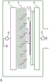
图1示出了布置在等离子体蚀刻室内的半导体衬底。FIG. 1 shows a semiconductor substrate arranged within a plasma etching chamber.
图2A示出了绝缘体上硅(SOI)晶体管器件的顶视图。Figure 2A shows a top view of a silicon-on-insulator (SOI) transistor device.
图2B示出了沿图2A的线AA的图2A的绝缘体上硅(SOI)晶体管器件的截面视图。SOI晶体管器件被示出为包括形成在有源层中的有源区以及在绝缘层顶部处制造的栅极多晶硅层的栅极多晶硅结构。2B shows a cross-sectional view of the silicon-on-insulator (SOI) transistor device of FIG. 2A along line AA of FIG. 2A . An SOI transistor device is shown as a gate polysilicon structure comprising an active region formed in an active layer and a gate polysilicon layer fabricated on top of an insulating layer.
图3A示出了用于向SOI晶体管器件的有源层和栅极多晶硅层提供放电路径的现有技术的实施方式。Figure 3A illustrates a prior art embodiment for providing a discharge path to the active layer and gate polysilicon layer of an SOI transistor device.
图3B示出了当器件在处理室内时图3A的现有技术器件的示意性表示。FIG. 3B shows a schematic representation of the prior art device of FIG. 3A when the device is within a processing chamber.
图3C示出了在器件的正常操作期间图3A的现有技术器件的示意性表示。Figure 3C shows a schematic representation of the prior art device of Figure 3A during normal operation of the device.
图4A示出了向SOI晶体管器件提供的根据本公开内容的一个实施方式的双s接触。s接触向SOI晶体管器件的有源层(源极区)和栅极多晶硅层提供放电路径。Figure 4A illustrates a dual s-contact provided to an SOI transistor device according to one embodiment of the present disclosure. The s-contact provides a discharge path to the active layer (source region) and gate polysilicon layer of the SOI transistor device.
图4B示出了向SOI晶体管器件提供的根据本公开内容的一个实施方式的双s接触。s接触向SOI晶体管器件的有源层(漏极区)和栅极多晶硅层提供放电路径。Figure 4B illustrates a dual s-contact provided to an SOI transistor device according to one embodiment of the present disclosure. The s-contact provides a discharge path to the active layer (drain region) and gate polysilicon layer of the SOI transistor device.
图4C至图4D示出了具有向晶体管器件的一个区域提供的根据本公开内容的一个实施方式的一个s接触的SOI晶体管器件。晶体管器件的其它区域可以电阻式耦接至向其它晶体管器件提供的s接触。4C-4D illustrate SOI transistor devices having an s-contact according to an embodiment of the present disclosure provided to a region of the transistor device. Other regions of the transistor devices may be resistively coupled to s-contacts provided to other transistor devices.
图4E示出了根据本公开内容的一个实施方式的各自具有一个s接触的两个相邻的晶体管器件。Figure 4E shows two adjacent transistor devices each having one s-contact according to one embodiment of the disclosure.
图4F示出了根据本公开内容的一个实施方式的与第一晶体管器件相关联的s接触与第二晶体管器件的电阻式耦接。FIG. 4F illustrates resistive coupling of an s-contact associated with a first transistor device to a second transistor device, according to one embodiment of the disclosure.
图4G至图4H示出了向SOI晶体管器件提供的根据本公开内容的一个实施方式的双s接触,其中s接触穿透晶体管器件的有源区。4G to 4H illustrate the provision of dual s-contacts according to one embodiment of the present disclosure to SOI transistor devices, where the s-contact penetrates through the active region of the transistor device.
图4I示出了向包括富陷阱层的SOI晶体管提供的根据本公开内容的一个实施方式的双s接触。FIG. 41 shows a double s-contact according to one embodiment of the present disclosure provided to an SOI transistor including a trap-rich layer.
图4J示出了当器件在处理室内时图4A的器件的示意性表示。FIG. 4J shows a schematic representation of the device of FIG. 4A when the device is within a processing chamber.
图4K示出了在器件的正常操作期间图4A的器件的示意性表示。Figure 4K shows a schematic representation of the device of Figure 4A during normal operation of the device.
图4L示出了当器件在处理室内时图4B的器件的示意性表示。FIG. 4L shows a schematic representation of the device of FIG. 4B when the device is within the processing chamber.
图4M示出了在器件的正常操作期间图4B的器件的示意性表示。Figure 4M shows a schematic representation of the device of Figure 4B during normal operation of the device.
图5A至图5B示出了根据本发明的配备有多个s接触的SOI晶体管器件的顶视图。5A-5B show top views of SOI transistor devices equipped with multiple s-contacts according to the present invention.
具体实施方式Detailed ways
贯穿本说明书,描述了实施方式和变型,用于示出本发明构思的用途和实现方式的目的。所说明的描述应当被理解为呈现本发明构思的示例,而不是限制本文所公开的构思的范围。Throughout this specification, embodiments and modifications have been described, for the purpose of illustrating uses and implementations of the inventive concept. The illustrated description should be understood as presenting an example of the inventive concepts, not as limiting the scope of the concepts disclosed herein.
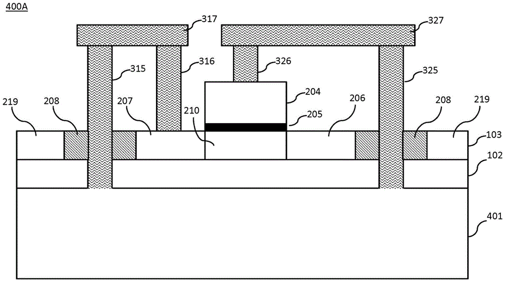
在本公开内容中描述了提供从顶上制造有绝缘(电绝缘)层的半导体器件的层的放电路径的设备和方法。根据本公开内容的各个实施方式的放电路径是纯电阻式路径,并且因此与现有技术实施方式相比结构更简单并且包括更少的制造步骤。这样的纯电阻式放电路径可以被提供给下述半导体器件:该半导体器件包括经由绝缘层与在下面的高电阻率衬底隔离的有源层。这样的示例性半导体器件为SOI MOSFET晶体管(例如,稍后描述的图4A的400A),其包括在晶体管的有源层(103)与高电阻率衬底(401)之间的绝缘掩埋氧化物层(BOX)(102),其中有源层(103)包括晶体管的栅极沟道(210)周围的晶体管的漏极(206)区和源极(207)区。在一些实施方式中,栅极沟道(210)通过作为栅极多晶硅层的一部分的相应的栅极多晶硅结构(204)来限定。Apparatus and methods for providing a discharge path from layers of a semiconductor device fabricated on top of an insulating (electrically insulating) layer are described in this disclosure. The discharge path according to various embodiments of the present disclosure is a purely resistive path and is therefore structurally simpler and includes fewer manufacturing steps than prior art embodiments. Such a purely resistive discharge path may be provided for a semiconductor device comprising an active layer isolated from an underlying high-resistivity substrate via an insulating layer. Such an exemplary semiconductor device is a SOI MOSFET transistor (e.g., 400A of FIG. 4A described later), which includes an insulating buried oxide between the active layer (103) of the transistor and the high-resistivity substrate (401). Layer (BOX) (102), wherein the active layer (103) includes a drain (206) region and a source (207) region of the transistor surrounding a gate channel (210) of the transistor. In some embodiments, the gate channel (210) is defined by a corresponding gate polysilicon structure (204) that is part of the gate polysilicon layer.
如本文中所使用的,表述“有源层”用于指示覆于掩埋氧化物层(BOX)(例如,102)上并且通过始于原始硅层的各种CMOS处理步骤而获得的层(例如,103)。有源层可以包括有源器件的有源区(例如,206、207、210、219)以及隔离区(例如,208)。在一些实施方式中,隔离区可以用于隔离有源层的相邻有源区。在一些实施方式中,有源层可以包括在有源层的区内创建的无源部件,例如电阻器。通常,电流流过的有源层的区可以被称为有源层的有源区。As used herein, the expression "active layer" is used to denote a layer (eg , 103). The active layer may include active regions (eg, 206, 207, 210, 219) of active devices and isolation regions (eg, 208). In some embodiments, isolation regions may be used to isolate adjacent active regions of the active layer. In some implementations, the active layer may include passive components, such as resistors, created within regions of the active layer. In general, a region of the active layer through which current flows may be referred to as an active region of the active layer.
如本文中所使用的,表述“栅极多晶硅层”用于指示形成有限定不同半导体器件的栅极沟道(例如,图2B的210)的栅极多晶硅结构(例如,图2B的204)的层(例如,图1的104)。栅极多晶硅层可以包括与不同的半导体器件相关联的连续和不连续的栅极多晶硅结构。As used herein, the expression "gate polysilicon layer" is used to refer to the layer of gate polysilicon structure (e.g., 204 of FIG. layer (eg, 104 of FIG. 1 ). The gate polysilicon layer may include continuous and discontinuous gate polysilicon structures associated with different semiconductor devices.
根据本公开内容的s接触可以通过将诸如有源层的有源区和栅极多晶硅层的栅极多晶硅结构的这样的层的区电阻式连接至其上制造层的高电阻率半导体衬底,提供至有源层和至栅极多晶硅层的电阻式放电路径。The s-contact according to the present disclosure may resistively connect regions of such layers as the active region of the active layer and the gate polysilicon structure of the gate polysilicon layer to the high-resistivity semiconductor substrate on which the layers are fabricated, A resistive discharge path is provided to the active layer and to the gate polysilicon layer.
如本文中所使用的,根据本公开内容的各个实施方式,半导体器件中的s接触是下述电阻式路径(例如,图4A至图4B的(315、316、317)或者(325、326、327)的组合):其提供半导体器件的层(例如,如图4A至图4B中所描绘的层103的区206、207或者层104的区204)的表面处的接触点与半导体器件的高电阻率衬底(例如,图4A至图4B的401)的表面处的接触点之间的电阻式导电路径。本领域技术人员将知道提供根据本公开内容的s接触的许多制造方法。As used herein, according to various embodiments of the present disclosure, an s-contact in a semiconductor device is a resistive path (eg, (315, 316, 317) or (325, 326, 327)): It provides a contact point at the surface of a layer of a semiconductor device (for example,
根据本公开内容的各个实施方式,用于s接触的材料可以是任何低电阻率导电材料,例如多晶硅和各种金属(例如,钨、铜等)。根据本公开内容的s接触可以具有相同材料,或包括若干材料,提供s接触(例如,图4A至图4B的(315、316、317)或(325、326、327))的分段构造。According to various embodiments of the present disclosure, the material used for the s-contact may be any low-resistivity conductive material, such as polysilicon and various metals (eg, tungsten, copper, etc.). The s-contacts according to the present disclosure may be of the same material, or comprise several materials, providing a segmented configuration of the s-contacts (eg ( 315 , 316 , 317 ) or ( 325 , 326 , 327 ) of FIGS. 4A-4B ).
根据本公开内容的实施方式,s接触穿透半导体器件的有源层(例如,图4A的103)的隔离区(例如,图4A的208),并且穿透半导体器件的绝缘层(例如,图4A的BOX层102)以到达并接触高电阻率衬底(例如,图4A的401)。在SOI器件的情况下,隔离区(208)可以是浅沟槽隔离(STI)区。应注意,通过穿透有源层(103)的隔离区(208),s接触在除了位于层(例如,层103或层104)的表面处的接触点之外的所有点处保持与半导体器件的有源区(例如,图4A的206、207、210)隔离。According to an embodiment of the present disclosure, the s-contact penetrates the isolation region (eg, 208 of FIG. 4A ) of the active layer (eg, 103 of FIG. 4A ) of the semiconductor device, and penetrates the insulating layer (eg, 103 of FIG. 4A BOX layer 102) to reach and contact the high-resistivity substrate (eg, 401 of FIG. 4A ). In the case of SOI devices, the isolation region (208) may be a shallow trench isolation (STI) region. It should be noted that by penetrating the isolation region (208) of the active layer (103), the s-contact remains connected to the semiconductor device at all points except the point of contact at the surface of the layer (e.g.,
根据本公开内容的又一实施方式,s接触在可以与器件的其它有源区(例如,图4A至图4I的206、207、210)隔离的有源层的有源区(例如,图4A至图4I的219)处穿透半导体器件的有源层(例如,图4A至图4I的103),并且穿透半导体器件的绝缘层(例如,图4A至图4I的BOX层102)以到达并且接触高电阻率衬底(例如,图4A至图4I的401)。可以经由隔离区(例如,图4A至图4I的208,其可以是STI区)提供有源层(103)内的有源区(206、207、210)的隔离。According to yet another embodiment of the present disclosure, the s-contact is in an active region (eg, FIG. 4A to 219 of FIG. 4I) to penetrate the active layer of the semiconductor device (for example, 103 of FIG. 4A to FIG. 4I), and penetrate the insulating layer of the semiconductor device (for example,
根据本公开内容的又一实施方式,可以针对同一半导体器件提供多个s接触(例如,图4A至图4B的(315、316、317)和(325、326、327))。这样的多个s接触可以被提供给半导体器件的形成在有源层(103)中的有源区(包括器件的漏极区(206)和/或源极区(207)),以及被提供给器件的形成在栅极多晶硅层(104)中的栅极多晶硅结构(204)。According to yet another embodiment of the present disclosure, multiple s-contacts (eg ( 315 , 316 , 317 ) and ( 325 , 326 , 327 ) of FIGS. 4A-4B ) may be provided for the same semiconductor device. Such a plurality of s-contacts may be provided to the active region of the semiconductor device formed in the active layer (103), including the drain region (206) and/or source region (207) of the device, and provided A gate polysilicon structure (204) is formed in the gate polysilicon layer (104) for the device.
根据本公开内容的又一实施方式,多个器件被形成在高电阻率衬底(401)上,并且多个s接触被提供给与所述多个器件相关联的有源层的有源区以及栅极多晶硅层的栅极多晶硅结构。According to yet another embodiment of the present disclosure, a plurality of devices are formed on a high-resistivity substrate (401), and a plurality of s-contacts are provided to active regions of active layers associated with the plurality of devices And the gate polysilicon structure of the gate polysilicon layer.
根据本公开内容的又一实施方式,与第一器件直接连接的s接触还可以提供至与第一器件电阻式耦接的其它器件的放电路径。第一器件和其它器件例如可以是电路的一部分,并且这样的电路的互连可以提供其它器件的一个或更多个有源区/栅极多晶硅结构与直接连接至s接触的第一器件的有源区/栅极多晶硅结构之间的电阻式耦接,从而有效地提供至其它器件的一个或更多个有源区/栅极多晶硅结构的电阻式放电路径。因此,包括多个器件(例如,晶体管)的电路可以被共享数目的s接触保护,其中经由多个器件的电阻式互相连接来提供共享。这可以有效保护多个器件的全部有源区和全部栅极多晶硅结构。换言之,电路的晶体管器件的任何有源区和栅极多晶硅结构具有至s接触的直接连接,或者经由电路互连被电阻式耦接至s接触。参照图4A,s接触(315、316、317)的导电接触部(316)与器件(400A)的有源区(207)直接连接。换言之,器件400A的有源区(207)具有至s接触(315、316、317)的直接连接,并且s接触被视为与器件(400A)相关联。According to yet another embodiment of the present disclosure, the s-contact directly connected to the first device may also provide a discharge path to other devices resistively coupled to the first device. The first device and other devices may, for example, be part of a circuit, and the interconnection of such a circuit may provide one or more active region/gate polysilicon structures of other devices with the active region of the first device directly connected to the s-contact. The resistive coupling between the source/gate polysilicon structures effectively provides a resistive discharge path to one or more active region/gate polysilicon structures of other devices. Thus, a circuit comprising multiple devices (eg, transistors) may be protected by a shared number of s-contacts, where sharing is provided via resistive interconnection of the multiple devices. This can effectively protect the entire active area and the entire gate polysilicon structure of multiple devices. In other words, any active regions and gate polysilicon structures of transistor devices of the circuit have a direct connection to the s-contact, or are resistively coupled to the s-contact via a circuit interconnect. Referring to Figure 4A, the conductive contact (316) of the s-contact (315, 316, 317) is directly connected to the active region (207) of the device (400A). In other words, the active region ( 207 ) of
根据本公开内容的另一实施方式,s接触经由第一导电接触部(例如,图4A的316和326)与半导体器件的区域(例如,204、206、207)接触,并且经由第二导电接触部(例如,图4A的315和325)与高电阻率衬底(401)接触,其中第一导电接触部和第二导电接触部经由导线(例如,图4A的317和327)导电连接。根据本公开内容的实施方式,导线是半导体器件的金属层的一部分。According to another embodiment of the present disclosure, the s-contact is in contact with a region (eg, 204, 206, 207) of the semiconductor device via a first conductive contact (eg, 316 and 326 of FIG. 4A ), and via a second conductive contact parts (eg, 315 and 325 of FIG. 4A ) are in contact with the high-resistivity substrate (401), wherein the first and second conductive contacts are conductively connected via wires (eg, 317 and 327 of FIG. 4A ). According to an embodiment of the present disclosure, the wire is part of a metal layer of a semiconductor device.
根据本公开内容的另一实施方式,在高电阻率衬底(401)与BOX层(102)之间可以设置富陷阱层(例如,图4I的402)。本领域技术人员容易理解通过在SOI器件中包括富陷阱层所提供的的益处,其描述在本公开内容的范围之外。在设置有富陷阱层的情况下,s接触(例如,图4I的325、326、327)还可以穿通富陷阱层(402)以与高电阻率衬底(401)(直接)接触,或者s接触(例如,315、316、317)可以穿透富陷阱层(402)足够深以通过富陷阱层的厚度的剩余部分与高电阻率衬底(401)进行电阻式接触。According to another embodiment of the present disclosure, a trap-rich layer (eg, 402 of FIG. 4I ) may be provided between the high-resistivity substrate ( 401 ) and the BOX layer ( 102 ). Those skilled in the art will readily appreciate the benefits provided by including a trap-rich layer in an SOI device, the description of which is outside the scope of this disclosure. In the case where a trap-rich layer is provided, the s-contact (for example, 325, 326, 327 of FIG. The contacts (eg, 315, 316, 317) may penetrate the trap-rich layer (402) deep enough to make resistive contact with the high-resistivity substrate (401 ) through the remainder of the thickness of the trap-rich layer.
如本文中所使用的,高电阻率衬底是具有在3000欧姆·厘米至20000欧姆·厘米或者更大的范围内的电阻率的衬底。可以通过对衬底的掺杂来控制衬底的电阻率,其中更轻的掺杂提供更高的衬底电阻率。如本领域技术人员所公知的,标准的SOI工艺使用具有1000欧姆·厘米以下的低电阻率的衬底。假使导电接触部(315、325)的小的横截面(例如,0.35μm×0.35μm)与高电阻率衬底(401)接触,由于随着电流向小的接触部聚集而产生的分布电阻以及由于因衬底(401)的轻度掺杂而产生的界面的非欧姆形状,在导电接触部(315、325)与高电阻率衬底(401)之间的有效接触电阻在0.2至20G欧姆的范围内。As used herein, a high resistivity substrate is a substrate having a resistivity in the range of 3000 Ohm·cm to 20000 Ohm·cm or greater. The resistivity of the substrate can be controlled by doping the substrate, with lighter doping providing higher substrate resistivity. As known to those skilled in the art, standard SOI processes use substrates with low resistivities below 1000 ohm·cm. If the small cross-section (for example, 0.35 μm x 0.35 μm) of the conductive contact (315, 325) is in contact with the high-resistivity substrate (401), due to the distributed resistance generated as the current gathers to the small contact and The effective contact resistance between the conductive contacts (315, 325) and the high resistivity substrate (401) is in the range of 0.2 to 20G ohms due to the non-ohmic shape of the interface due to light doping of the substrate (401) In the range.
如在本公开内容的下面部分中所呈现的,根据本公开内容的各种实施方式的s接触可以通过经由导线连接两个导电接触部来提供,其中通过穿通半导体器件的绝缘层以及可选地穿通富陷阱层,第一导电接触部连接至半导体器件的有源层或栅极多晶硅层,并且第二导电接触部连接至半导体器件的高电阻率衬底。此外,s接触进而可以经由公共电路的电阻式互连被电阻式耦接至不同的半导体器件的有源层或栅极多晶硅层。如上所述,可以经由分别连接至有源层的有源区和连接至栅极多晶硅层的栅极多晶硅结构的导电接触部来制造至有源层和栅极多晶硅层的连接。As presented in the following sections of the present disclosure, s-contacts according to various embodiments of the present disclosure may be provided by connecting two conductive contacts via wires, by punching through the insulating layer of the semiconductor device and optionally Through the trap-rich layer, the first conductive contact is connected to the active layer or the gate polysilicon layer of the semiconductor device, and the second conductive contact is connected to the high-resistivity substrate of the semiconductor device. Furthermore, the s-contacts may in turn be resistively coupled to active layers or gate polysilicon layers of different semiconductor devices via a resistive interconnection of a common circuit. As mentioned above, connections to the active layer and the gate polysilicon layer may be made via conductive contacts of the gate polysilicon structure connected to the active region of the active layer and to the gate polysilicon layer, respectively.
本文中所描述的实施方式是通过N型MOSFET器件来例示的。本领域普通技术人员将容易理解,可以通过适当地应用不同类型的掺杂方案而将本文中所公开的发明构思应用于其它类型的半导体器件,例如P型MOSFET器件。根据本发明的实施方式还可以应用于扩展的漏极器件,例如横向扩散金属氧化物半导体(LDMOS)器件,以及包括有源层与高电阻率衬底之间的绝缘层的其它的门控晶体管或者器件。Embodiments described herein are exemplified by N-type MOSFET devices. Those of ordinary skill in the art will readily understand that the inventive concepts disclosed herein can be applied to other types of semiconductor devices, such as P-type MOSFET devices, by appropriately applying different types of doping schemes. Embodiments in accordance with the present invention may also be applied to extended drain devices, such as laterally diffused metal-oxide-semiconductor (LDMOS) devices, and other gated transistors that include an insulating layer between an active layer and a high-resistivity substrate or device.
具有根据本公开内容的各种实施方式的s接触的半导体器件可以包括形成在绝缘体上硅(SOI)上的半导体器件,包括场效应晶体管(FET)。FET器件可以包括互补金属氧化物半导体(CMOS)、金属氧化物半导体场效应晶体管(MOSFET)以及其它类型的场效应晶体管(FET)器件。Semiconductor devices having s-contacts according to various embodiments of the present disclosure may include semiconductor devices formed on silicon-on-insulator (SOI), including field effect transistors (FETs). FET devices may include complementary metal oxide semiconductor (CMOS), metal oxide semiconductor field effect transistor (MOSFET), and other types of field effect transistor (FET) devices.
在根据本公开内容的一个示例性实施方式中,s接触可以包括方形或矩形的导电接触部。如将在本公开内容的后面部分中所描述的,s接触可以提供在半导体器件的顶层的区域至高电阻率衬底之间的低电阻率导电路径,因此提供针对在制造过程期间注入的电荷的放电路径。In one exemplary embodiment according to the present disclosure, the s-contact may include a square or rectangular conductive contact. As will be described later in this disclosure, s-contacts can provide a low-resistivity conductive path between regions of the top layer of a semiconductor device to a high-resistivity substrate, thus providing protection against charge injected during the fabrication process. discharge path.
对于根据本公开内容的SOI MOSFET晶体管的示例性实施方式,可以向晶体管的源极区和/或漏极区提供一个或更多个s接触。替选地或者另外地,可以向晶体管的栅极多晶硅结构提供一个或更多个s接触。For example embodiments of SOI MOSFET transistors according to the present disclosure, one or more s-contacts may be provided to the source and/or drain regions of the transistor. Alternatively or additionally, one or more s-contacts may be provided to the gate polysilicon structure of the transistor.
对于包括具有相应有源区和栅极多晶硅结构的多个互连的SOI MOSFET晶体管的电路的示例性实施方式,可以向电路的一些或所有晶体管的有源区提供一个或更多个s接触,并且可以向电路的一些或所有晶体管的栅极多晶硅结构提供一个或更多个s接触。在一个示例性实施方式中,电路互连可以提供从第一晶体管的有源区和/或栅极多晶硅结构至第二晶体管的s接触的电阻式耦接,因此提供了至第一晶体管的放电路径。For an exemplary embodiment of a circuit comprising a plurality of interconnected SOI MOSFET transistors with corresponding active regions and gate polysilicon structures, one or more s-contacts may be provided to the active regions of some or all transistors of the circuit, And one or more s-contacts may be provided to the gate polysilicon structure of some or all transistors of the circuit. In one exemplary embodiment, the circuit interconnect may provide a resistive coupling from the active region and/or gate polysilicon structure of the first transistor to the s-contact of the second transistor, thus providing a discharge to the first transistor path.
根据本公开内容的另一实施方式,在半导体器件中s接触的数目和相应空间布置可以被设置为限制在电荷注入过程(例如,等离子体蚀刻)期间跨越半导体器件的任意两个点的电势。给定已知的衬底的高电阻率值以及在电荷注入过程期间通过s接触的感应电流,可以导出限制这样的电势差的s接触的数目。这可以在模拟软件的帮助下来执行。本领域技术人员应理解,由于根据本发明的s接触的纯电阻性质,在同s接触的添加相关联的半导体器件工作期间的泄露电流与在器件的制造期间提供对s接触的保护的量之间存在权衡。According to another embodiment of the present disclosure, the number and corresponding spatial arrangement of s-contacts in a semiconductor device may be set to limit the potential across any two points of the semiconductor device during a charge injection process (eg, plasma etching). Given the known high resistivity value of the substrate and the induced current through the s-contact during the charge injection process, the number of s-contacts that limits such a potential difference can be derived. This can be performed with the help of simulation software. Those skilled in the art will appreciate that due to the purely resistive nature of the s-contact according to the present invention, the leakage current during operation of the semiconductor device associated with the addition of the s-contact is related to the amount of protection provided to the s-contact during fabrication of the device. There is a trade-off between.
图1示出了放置在示例性高能制造处理室(100)内的半导体衬底(101)。半导体衬底(101)包括:有源硅层(103),其包括具有相应导电接触部的有源部件的有源区;以及(栅极)多晶硅层(104),其包括具有在多晶硅层(104)上的相应导电接触部的栅极多晶硅结构。有源层(103)覆在绝缘层(102)上,绝缘层(102)防止在有源层(103)与衬底(101)之间的传导。衬底(101)位于室的在与底部电势(190)连接的底电极(160)上。室的顶电极(150)连接至可变供给(180)。在示例性处理室(100)内,半导体衬底(101)能够经受以下事件:其可以在半导体衬底(101)上产生电势梯度或感生电荷,从而导致注入电荷保持被俘获在层(103)、(104)内或者在这样的层之间的界面处,以及在衬底的处理阶段期间产生在这样的层与衬底(101)之间的大的电势差。这些层内被俘获的电荷可以不利地影响有源部件的工作特征(例如,阈值电压的改变、泄露特性的改变等),同时在这些层与衬底之间的大的电势差可以潜在地损坏有源层的有源部件,使得它们无功能。通过经由在半导体层(103)和(104)的表面处的接触部向耦接至底电极(160)的底部电势(190)提供放电路径,可以防止(例如,消除)电荷注入到这样的半导体层中。Figure 1 illustrates a semiconductor substrate (101) placed within an exemplary high energy manufacturing process chamber (100). The semiconductor substrate (101) comprises: an active silicon layer (103) comprising active regions of active components with corresponding conductive contacts; and a (gate) polysilicon layer (104) comprising 104) on the gate polysilicon structure of the corresponding conductive contact. The active layer (103) overlies the insulating layer (102), and the insulating layer (102) prevents conduction between the active layer (103) and the substrate (101). The substrate (101) is located on the bottom electrode (160) of the chamber which is connected to the bottom potential (190). The top electrode (150) of the chamber is connected to a variable supply (180). Within the exemplary processing chamber (100), the semiconductor substrate (101) can be subjected to events that can create a potential gradient or induce charge across the semiconductor substrate (101), causing the injected charge to remain trapped in the layer (103 ), (104) or at the interface between such layers, and during the processing phase of the substrate generate large potential differences between such layers and the substrate (101). Trapped charges within these layers can adversely affect the operating characteristics of active components (e.g., changes in threshold voltage, changes in leakage characteristics, etc.), while large potential differences between these layers and the substrate can potentially damage active components. Active components of the source layer, rendering them non-functional. By providing a discharge path to the bottom potential (190) coupled to the bottom electrode (160) via contacts at the surfaces of the semiconductor layers (103) and (104), charge injection into such semiconductor layers can be prevented (eg eliminated) layer.
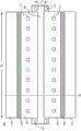
图2A示出N型SOI MOSFET器件(200)的顶视图,其可以是形成在覆于半导体衬底(101)上的有源层中的有源部件的一部分。器件(200)的栅极指(204)被示出为位于源极区(207)与漏极区(206)之间。栅极指(204)具有长度LG和宽度WG。在一个方面,栅极指可以经由栅极多晶硅结构(204)来制造,被形成在多晶硅层(104)内,这可以阻断用于掺杂MOSFET的相邻源极区和漏极区的掺杂剂离子注入。本领域技术人员容易认识到多指SOI器件可以具有电耦接的多个这样的指状件,其中每个指状件可以包括具有相应栅极接触部(213)的相应栅极多晶硅结构(204),具有相应漏极接触部(212)的漏极区(206),以及具有相应源极接触部(211)的源极区(207)。在一些实施方式中,相邻指状件可以共享相应漏极区和/或源极区。替选地,对应于多个晶体管器件的多个指状件可以共用相同的公共半导体衬底(101)并且相对于彼此电隔离。器件(200)的有源区(206、207)相对于形成在半导体衬底(101)上的其它有源区(219)的隔离可以经由隔离区(208)来提供。普通技术人员将认识到图2A的标记区域以外的区域可以包括有源区(219)或隔离区(208)。Figure 2A shows a top view of an N-type SOI MOSFET device (200), which may be part of an active component formed in an active layer overlying a semiconductor substrate (101). The gate fingers (204) of the device (200) are shown positioned between the source region (207) and the drain region (206). Gate fingers (204) have a length LG and a width WG. In one aspect, the gate fingers can be fabricated via a gate polysilicon structure (204), formed within the polysilicon layer (104), which can block the doping used to dope the adjacent source and drain regions of the MOSFET. Dopant ion implantation. Those skilled in the art will readily recognize that a multi-finger SOI device may have a plurality of such fingers electrically coupled, wherein each finger may include a respective gate polysilicon structure (204) with a respective gate contact (213). ), a drain region (206) with a corresponding drain contact (212), and a source region (207) with a corresponding source contact (211). In some implementations, adjacent fingers may share respective drain and/or source regions. Alternatively, multiple fingers corresponding to multiple transistor devices may share the same common semiconductor substrate (101) and be electrically isolated with respect to each other. Isolation of the active regions (206, 207) of the device (200) from other active regions (219) formed on the semiconductor substrate (101) may be provided via the isolation region (208). One of ordinary skill will recognize that regions other than the marked region of FIG. 2A may include active regions (219) or isolation regions (208).
图2B示出了沿图2A的线AA的N型SOI MOSFET器件(200)的截面视图。如图2B的截面视图所示,SOI MOSFET包括形成在衬底(101)顶上的层结构,其包括层(102)、(103)、(204)和(205)。在一个方面,形成器件的栅极多晶硅结构的层(204)被示出为放置在绝缘栅氧化硅层(205)上方。在一个方面,在层(204)下方的本体区(210)掺杂有P型掺杂剂(P本体),并且源极(207)区和漏极(206)区重注入有N型掺杂剂(N+)。如在附图中所示,区域(206)、(207)和(210)是有源层(103)的置于绝缘掩埋氧化物(BOX)层(103)的部分。另外,如图2A和图2B所示,器件(200)被示出为通过浅沟槽隔离(STI)区(208)与有源层(103)内的相邻区域(其可以包含包括其它指状件/晶体管的相邻电路,未示出)隔离,浅沟槽隔离(STI)区(208)为非导电型。由于BOX层(102)的绝缘性质,没有在如图2A和图2B中所描绘的SOI MOSFET中提供在层(103)、(204)和(205)与半导体衬底(101)之间的导电路径,因此器件(200)在高电势制造过程期间易于电荷注入。Figure 2B shows a cross-sectional view of the N-type SOI MOSFET device (200) along line AA of Figure 2A. As shown in the cross-sectional view of Figure 2B, the SOI MOSFET comprises a layer structure formed on top of a substrate (101), comprising layers (102), (103), (204) and (205). In one aspect, a layer (204) forming a gate polysilicon structure of the device is shown placed over an insulating gate silicon oxide layer (205). In one aspect, the body region (210) below the layer (204) is doped with P-type dopants (P body), and the source (207) and drain (206) regions are re-implanted with N-type dopants agent (N+). As shown in the figure, regions (206), (207) and (210) are portions of the active layer (103) that are disposed in an insulating buried oxide (BOX) layer (103). Additionally, as shown in FIGS. 2A and 2B , the device ( 200 ) is shown as being connected to adjacent regions within the active layer ( 103 ) (which may include other references) via a shallow trench isolation (STI) region ( 208 ). Neighboring circuits of devices/transistors, not shown), the shallow trench isolation (STI) region (208) is non-conductive. Due to the insulating nature of the BOX layer (102), no electrical conduction between the layers (103), (204) and (205) and the semiconductor substrate (101) is provided in SOI MOSFETs as depicted in Figures 2A and 2B. path, so the device (200) is susceptible to charge injection during the high potential fabrication process.
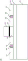
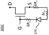
图3A示出了SOI MOSFET器件(300)的现有技术实施方式,其提供了在栅极多晶硅结构(204)上的接触部(326)与半导体衬底(101)之间的第一放电路径以及在器件(300)的源极区(207)上的接触部(316)与半导体衬底(101)之间的第二放电路径。本领域技术人员将认识到图3A没有示出SOI MOSFET的精确截面,这是由于到栅极多晶硅结构(204)的接触部(326)通常具有与接触部(316)到源极区(207)的截面平面不同的截面平面。Figure 3A shows a prior art implementation of a SOI MOSFET device (300) providing a first discharge path between a contact (326) on a gate polysilicon structure (204) and a semiconductor substrate (101) And a second discharge path between the contact (316) on the source region (207) of the device (300) and the semiconductor substrate (101). Those skilled in the art will recognize that FIG. 3A does not show the exact cross-section of the SOI MOSFET since the contact (326) to the gate polysilicon structure (204) typically has the same contact (316) to the source region (207) The cross-section planes are different from the cross-section planes.
如在图3A中所描绘的现有技术实施方式中可以看出,第一放电路径包括导电接触部(326)、导线(327)、导电接触部(325)、N型掺杂区(345)和半导体衬底(101)。导电接触部(325,326)和导线(327)可以由金属(如铜或钨)制成。此外,埋置在半导体衬底(101)内的N型掺杂区(345)以及与区(345)接触的衬底(101)的P型掺杂区创建了结型二极管。因此,第一放电路径使栅极多晶硅层(204)经由结型二极管耦接至半导体衬底(101)。As can be seen in the prior art embodiment depicted in Figure 3A, the first discharge path includes a conductive contact (326), a wire (327), a conductive contact (325), an N-type doped region (345) and a semiconductor substrate (101). The conductive contacts (325, 326) and wires (327) may be made of metal such as copper or tungsten. Furthermore, the N-type doped region (345) buried within the semiconductor substrate (101) and the P-type doped region of the substrate (101) in contact with the region (345) create a junction diode. Therefore, the first discharge path couples the gate polysilicon layer (204) to the semiconductor substrate (101) via a junction diode.
在图3A中所描绘的现有技术器件(300)的第二放电路径包括导电接触部(316)、导线(317)、导电接触部(315)、P型掺杂区(340)和半导体衬底(101)。与第一放电路径类似,导电接触部(315,316)和导线(317)可以由金属(如铜或钨)制成。The second discharge path of the prior art device (300) depicted in FIG. 3A includes a conductive contact (316), a wire (317), a conductive contact (315), a P-type doped region (340) and a semiconductor substrate Bottom (101). Similar to the first discharge path, the conductive contacts (315, 316) and wires (317) may be made of metal such as copper or tungsten.
应当注意,现有技术器件(300)的第一放电路径和第二放电路径使导电接触部(315)和(325)分别经由区域(340)和(345)耦接至半导体衬底(101)。因此在图3A所描绘的现有技术实施方式中不存在这种接触部与半导体衬底(101)之间的直接接触。It should be noted that the first and second discharge paths of the prior art device (300) couple the conductive contacts (315) and (325) to the semiconductor substrate (101) via regions (340) and (345), respectively . There is therefore no direct contact between such contacts and the semiconductor substrate (101 ) in the prior art embodiment depicted in FIG. 3A .
当将现有技术器件(300)放置在处理室(100)中时,通过第一放电路径的元件(345)和(101)形成的结型二极管允许电荷(例如电子)从多晶硅层(104)的栅极多晶硅结构(204)向底电极板流动,半导体衬底(101)耦接到该底电极板。类似地,第二放电路径允许电荷从有源层(103)的源极区(207)至底部电极板流动,半导体衬底(101)耦接到底部电极板。本领域技术人员将认识到结型二极管对于处理室的内部产生的电流可能泄露,因此电荷可以沿任一方向流动。When the prior art device (300) is placed in the processing chamber (100), the junction diode formed by the elements (345) and (101) of the first discharge path allows charges (e.g. electrons) to flow from the polysilicon layer (104) The gate polysilicon structure (204) flows towards the bottom electrode plate to which the semiconductor substrate (101) is coupled. Similarly, the second discharge path allows charge to flow from the source region (207) of the active layer (103) to the bottom electrode plate to which the semiconductor substrate (101) is coupled. Those skilled in the art will recognize that junction diodes can be leaky to currents generated inside the chamber, so charge can flow in either direction.
在图3A中所描绘的现有技术器件(300)中,半导体衬底(101)具有低电阻率,并且因此可以提供衬底(101)内部的任意两个区包括区(340)和(345)之间的低电阻导电路径。因此,需要通过现有技术器件(300)的区(345,101)形成的结型二极管,例如,以使在器件的正常操作期间不允许在栅极接触部(326)与源极接触部(316)之间的导电路径(例如,经由半导体衬底(101)在导电接触部(315)与(325)之间提供的低电阻率路径)。In the prior art device (300) depicted in FIG. 3A, the semiconductor substrate (101) has low resistivity, and thus any two regions inside the substrate (101) including regions (340) and (345) can be provided. ) between low resistance conductive paths. Therefore, there is a need for a junction diode formed by the regions (345, 101) of the prior art device (300), for example, such that during normal operation of the device no contact between the gate contact (326) and the source contact ( 316) (eg, a low-resistivity path provided between the conductive contacts (315) and (325) via the semiconductor substrate (101)).
图3B和图3C示意性表示了采用配置(300B)和配置(300C)的现有技术器件(300),在配置(300B)中器件在处理室(100)内,在配置(300C)中器件在正常操作期间。这些图示出了两个配置(300B)和(300C)中的每个配置的晶体管器件(300)和相应导电路径。电阻器δR2表示(325,326,327)的组合(低)电阻,电阻器δR1表示(315,316,317)的组合(低)电阻,项(375)表示由(345)和(101)的相邻区形成的结型二极管,δr0表示器件(300)的区(340)与区(345)之间的低电阻率路径的电阻,并且(δr1,δr2)表示区(340,345)中的每个与处理腔的底电极(其提供低参考电位,诸如地)之间的低电阻率路径的电阻。本领域技术人员将理解,电阻(δr0,δr1,δr2)由低电阻率半导体衬底(101)来提供。Figures 3B and 3C schematically illustrate a prior art device (300) in a configuration (300B) and a configuration (300C) in which the device is inside the chamber (100) and in a configuration (300C) in which the device during normal operation. These figures show the transistor device ( 300 ) and corresponding conductive paths for each of the two configurations ( 300B) and ( 300C ). Resistor δR2 represents the combined (low) resistance of (325,326,327), resistor δR1 represents the combined (low) resistance of (315,316,317), item (375) represents the junction diode formed by the adjacent regions of (345) and (101) , δr0 represents the resistance of the low-resistivity path between region (340) and region (345) of device (300), and (δr1, δr2) represents the connection between each of regions (340, 345) and the bottom electrode of the processing chamber (which A resistor that provides a low-resistivity path between a low reference potential, such as ground. Those skilled in the art will appreciate that the resistances (δr0, δr1, δr2) are provided by the low-resistivity semiconductor substrate (101).
进一步参考图3C,如上所述,由于现有技术实施方式器件(300)的衬底(101)的低电阻率性质,所以需要二极管(375)以便不通过源极提供栅极的电流负荷。本领域的技术人员将注意到所需的二极管(375)仅在栅极电压VG高于源极电压VS的晶体管器件(300)操作的期间阻挡器件的栅极(G)与源极(S)之间的电流流动,从而使二极管(375)置于反向偏置情况。因此,现有技术实施方式假设在器件(300)的正常操作期间栅极电压不低于源极电压,由于这样的条件使二极管(375)置于正向偏置情况,并防止期望的器件的负偏置(VG<VS)。Referring further to Fig. 3C, as mentioned above, due to the low resistivity nature of the substrate (101) of the prior art embodiment device (300), a diode (375) is required in order not to provide the current load of the gate through the source. Those skilled in the art will note that the required diode (375) blocks the gate (G) and source (S) of the device only during the period of operation of the transistor device (300) where the gate voltage VG is higher than the source voltage VS. Current flows between , thereby placing the diode (375) in a reverse biased condition. Therefore, prior art embodiments assume that the gate voltage does not fall below the source voltage during normal operation of the device (300), since such a condition places the diode (375) in a forward biased condition and prevents the desired Negative bias (VG<VS).
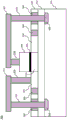
图4A示出了根据本公开内容的设置有s接触的SOI MOSFET器件(400A)的示例性实施方式。第一s接触(326,327,325)提供形成在多晶硅层(104)中的栅极多晶硅结构(204)上的接触部(326)与半导体衬底(401)之间的第一放电路径,并且第二s接触(316,317,315)提供形成于器件(400A)的有源区(103)中的源极区(207)上的接触部(316)与半导体衬底(401)之间的第二放电路径。通过使用高电阻率半导体衬底(401),s接触以及由此根据本发明的器件(400A)的第一放电路径和第二放电路径可能缺乏有源器件(例如,关于上述图3A至图3C所描绘的现有技术实施方式描述的二极管(375))并且可以保持纯电阻。因此,可以以根据本发明的器件的更简单的结构和更少的制造步骤来维持高能过程期间的保护功效。Figure 4A shows an exemplary embodiment of a SOI MOSFET device (400A) provided with s-contacts according to the present disclosure. The first s-contact (326, 327, 325) provides a first discharge path between the contact (326) formed on the gate polysilicon structure (204) in the polysilicon layer (104) and the semiconductor substrate (401), and the second s-contact The contacts (316, 317, 315) provide a second discharge path between the contact (316) formed on the source region (207) in the active region (103) of the device (400A) and the semiconductor substrate (401). By using a high-resistivity semiconductor substrate (401), the s-contact and thus the first and second discharge paths of the device (400A) according to the present invention may lack active devices (eg, with respect to FIGS. 3A-3C described above The depicted prior art embodiment describes a diode (375)) and may remain purely resistive. Thus, the protective efficacy during high-energy processes can be maintained with a simpler structure and fewer manufacturing steps of the device according to the invention.
如可以在根据图4A所描绘的公开内容的实施方式中看到的,第一放电路径(s接触)包括与栅极多晶硅结构(204)形成接触的导电接触部(326)、导线(327)以及与半导体衬底(401)形成直接接触的导电接触部(325)(与图3A所描绘的现有技术实施方式相反,其中接触是间接的并且通过创造结型二极管的耦接区(345))。类似地,第二放电路径(s接触)包括与源极区(207)形成接触的导电接触部(316)、导线(317)以及与半导体衬底(401)形成直接接触的导电接触部(315)。在本公开内容的示例性实施方式中,导电接触部(315,316,325,326)和导线(317,327)可以由如铜或钨的金属制成。在根据本公开内容的替选实施方式中,这样的接触部可以由包括其它金属和多晶硅的任意低电阻率导电材料制成。As can be seen in an embodiment of the disclosure as depicted in FIG. 4A , the first discharge path (s-contact) includes a conductive contact (326) making contact with the gate polysilicon structure (204), a wire (327) and a conductive contact (325) that makes direct contact with the semiconductor substrate (401) (in contrast to the prior art embodiment depicted in FIG. ). Similarly, the second discharge path (s-contact) includes a conductive contact (316) in contact with the source region (207), a wire (317), and a conductive contact (315) in direct contact with the semiconductor substrate (401). ). In an exemplary embodiment of the present disclosure, the conductive contacts (315, 316, 325, 326) and wires (317, 327) may be made of a metal such as copper or tungsten. In alternative embodiments according to the present disclosure, such contacts may be made of any low resistivity conductive material including other metals and polysilicon.
根据本公开内容的另外的实施方式,s接触可以电阻式耦接至其它器件的区域(例如,源极、漏极、栅极多晶硅),因而有效为这样的区域提供注入电荷的放电路径。According to further embodiments of the present disclosure, s-contacts may be resistively coupled to other device regions (eg, source, drain, gate polysilicon), thus effectively providing such regions with a discharge path for injected charges.
进一步参考图4A,本领域的技术人员易于认识到,根据本公开内容的第一放电路径和第二放电路径(s接触)两者是纯电阻式路径,并且因此可以允许来自路径两端的对称的电荷流。这意味着本发明提供注入电荷的放电路径,而与由图1的源极(180,190)提供的电势梯度的极性无关。此外,器件的正常操作期间的放电路径(以及由此在器件的源极与栅极之间)的去耦由提供接触部(315)与(325)之间的高电阻路径的半导体衬底(401)的高电阻率性质来提供。这意味着与图3A至图3C所描绘的现有技术实施方式相反,本发明在器件的正常操作期间允许器件的栅极相对于源极任意偏置,包括根据本发明的器件的负偏置(VG<VS)。本领域的技术人员将理解,如负偏置的这样的灵活性在一些RF开关实现中可以提供例如较高的输入/输出隔离。With further reference to FIG. 4A , those skilled in the art will readily recognize that both the first and second discharge paths (s-contacts) according to the present disclosure are purely resistive paths and thus may allow symmetrical charge flow. This means that the present invention provides a discharge path for the injected charges irrespective of the polarity of the potential gradient provided by the sources (180, 190) of FIG. 1 . Furthermore, the decoupling of the discharge path (and thus between the source and gate of the device) during normal operation of the device is provided by the semiconductor substrate ( 401) to provide high resistivity properties. This means that in contrast to the prior art implementation depicted in Figures 3A-3C, the present invention allows arbitrary biasing of the gate of the device with respect to the source during normal operation of the device, including negative biasing of the device according to the present invention (VG<VS). Those skilled in the art will appreciate that such flexibility as negative biasing may provide, for example, higher input/output isolation in some RF switch implementations.
根据本公开内容的另外的实施方式,如图4B所描绘的,以在如上所述的两条路径的(经由高电阻率路径的)相同的去耦等级,可以将第二放电路径提供至晶体管器件的漏极区而不是源极区。According to a further embodiment of the present disclosure, a second discharge path may be provided to the transistor as depicted in FIG. 4B at the same level of decoupling (via the high resistivity path) of both paths as described above The drain region of the device rather than the source region.
根据本公开内容的另外的实施方式,可以提供与源极区(207)、漏极区(206)和栅极多晶硅结构(204)中的每个分离且共存的s接触(放电路径)。本实施方式表示由图4A和4B示出的实施方式的组合。稍后描述的图5A和图5B示出了这样的组合。According to further embodiments of the present disclosure, separate and co-existing s-contacts (discharge paths) may be provided with each of the source region (207), drain region (206) and gate polysilicon structure (204). The present embodiment represents a combination of the embodiments shown in FIGS. 4A and 4B . 5A and 5B described later show such a combination.
根据本发明的半导体器件可以设置有一个、两个或更多个s接触,每个s接触具有至器件的漏极/源极区和/或栅极多晶硅结构的直接连接。图4A至图4B示出了根据本公开内容的具有各自直接连接(直接连接)至器件的漏极/源极区以及栅极多晶硅结构的s接触的半导体器件。图4C至图4D示出了根据本公开内容的具有直接连接至器件的栅极多晶硅结构(204)(图4C)的s接触(325,326,327)或者器件的漏极/源极区(206/207)(图4D)的s接触(315,316,317)的半导体器件(400C,400D)。如上所述,尽管半导体器件(400C,400D)不包括到器件的有源区(例如,206,207)和器件的栅极多晶硅结构两者的s接触的直接连接,但是可以向半导体器件(400C,400D)提供至具有到不同半导体器件的直接连接的s接触的电阻式耦接(连接)。A semiconductor device according to the invention may be provided with one, two or more s-contacts, each s-contact having a direct connection to the drain/source region and/or gate polysilicon structure of the device. 4A-4B illustrate a semiconductor device having s-contacts each directly connected (directly connected) to the device's drain/source region and gate polysilicon structure in accordance with the present disclosure. 4C-4D illustrate s-contacts (325, 326, 327) with direct connection to the device's gate polysilicon structure (204) (FIG. 4C) or the device's drain/source regions ( 206/207) (FIG. 4D) of the s-contacts (315, 316, 317) of the semiconductor device (400C, 400D). As mentioned above, although the semiconductor device (400C, 400D) does not include a direct connection to the s-contact of both the device's active region (e.g., 206, 207) and the device's gate polysilicon structure, it is possible to , 400D) provide resistive coupling (connection) to s-contacts with direct connections to different semiconductor devices.
图4E示出了制造在同一高电阻率半导体衬底(401)上的图4C和图4D的两个半导体器件(400C,400D)的示例性配置。如图4E中可以看到的那样,s接触(325,326,327)以及(315,316,317)中的每个在层(103)的隔离区(208)处穿透该层,该隔离区隔离两个半导体器件的有源区(例如,205,206,207)。在图4E中描绘的根据本公开内容的示例性实施方式中,两个s接触被示出为穿透同一(连续的)隔离区(208)。本领域技术人员将知道不将这样的示例性实施方式认为限制发明人认为是其发明的内容,因为例如隔离区(208)不必是连续区域,并且每个s接触可以穿透不同的且非连续的隔离区。Figure 4E shows an exemplary configuration of the two semiconductor devices (400C, 400D) of Figures 4C and 4D fabricated on the same high-resistivity semiconductor substrate (401). As can be seen in Figure 4E, each of the s-contacts (325, 326, 327) and (315, 316, 317) penetrates the layer (103) at an isolated region (208) of the layer, the isolated Regions isolate the active regions (eg, 205, 206, 207) of the two semiconductor devices. In an exemplary embodiment according to the present disclosure depicted in FIG. 4E, two s-contacts are shown penetrating the same (contiguous) isolation region (208). Those skilled in the art will appreciate that such exemplary embodiments are not to be considered limiting of what the inventors consider their invention, since, for example, the isolation region (208) need not be a contiguous region, and each s-contact may penetrate a different and non-contiguous quarantine area.
根据本公开内容的另一示例性实施方式,如图4F中所描绘的那样,与两个不同半导体器件(400C,400D)相关联的s接触可以在不同的(非连续的)隔离区(208)处穿透层(103)。图4F中描绘的根据本公开内容的示例性实施方式示出了用于(例如经由元件425,426,427,219,415,417)将第一器件(400C)的有源区(206)电阻式耦接至s接触(315,316,317)的一个示例性配置,其中s接触(315,316,317)直接连接至第二器件(400D)的有源区,第一器件和第二器件具有由隔离区(208)分隔的其相应的有源区(206,207,210)。According to another exemplary embodiment of the present disclosure, as depicted in FIG. 4F, s-contacts associated with two different semiconductor devices (400C, 400D) may be in different (non-contiguous) isolation regions (208 ) at the penetrating layer (103). An exemplary embodiment according to the present disclosure depicted in FIG. 4F shows an active region ( 206 ) resistive An exemplary configuration in which the s-contact (315, 316, 317) is coupled directly to the active region of the second device (400D), the first device and the second device have their respective active regions (206, 207, 210) separated by isolation regions (208).
如图4F中描绘的示例性实施方式中可以看到的那样,器件(400C)的漏极区(206)经由导电接触部(425)、导线(427)和导电接触部(426)连接至形成在层(103)内的有源区(219)。有源区(219)进而在导电接触部(426)与导电接触部(415)之间提供电阻式导电路径。最终,导电接触部(415)经由导线(417)被电阻式耦接至s接触(315,316,317)的导电接触部(315),由此在第一器件(400C)的源极区(206)与第二器件(400D)的s接触(315,316,317)之间提供电阻式耦接。As can be seen in the exemplary embodiment depicted in FIG. 4F , the drain region ( 206 ) of the device ( 400C ) is connected via a conductive contact ( 425 ), a wire ( 427 ) and a conductive contact ( 426 ) to the formed An active region (219) within layer (103). The active region (219) in turn provides a resistive conductive path between the conductive contact (426) and the conductive contact (415). Finally, the conductive contact (415) is resistively coupled to the conductive contact (315) of the s-contact (315, 316, 317) via a wire (417), whereby in the source region ( 206) to provide a resistive coupling between the s-contacts (315, 316, 317) of the second device (400D).
进一步参照图4F,尽管出于清楚原因未示出有源区(219),但有源区(219)可以包括可在两个接触部(426)与(415)之间提供电阻式导电路径的任何有源或无源部件。这可以包括例如一个或更多个电阻器、一个或更多个晶体管以及相关互连的组合,这些组合起来提供两个导电接触部(426)与(415)之间的电阻式导电路径(因此相对于电流对称),由此将第一器件(400C)的有源区(206)电阻式耦接至下述s接触,该s接触直接连接至第二器件(400D)的有源区(207)。本领域技术人员将理解,可以提供类似的配置用于将第一器件的栅极多晶硅区电阻式耦接至下述s接触,该s接触直接连接至第二器件的区域(例如,栅极多晶硅结构),这两个装置经由一个或更多个隔离区(208)被分隔开。With further reference to Figure 4F, although the active region (219) is not shown for reasons of clarity, the active region (219) may include a any active or passive components. This may include, for example, a combination of one or more resistors, one or more transistors, and associated interconnects that combine to provide a resistive conductive path between the two conductive contacts (426) and (415) (thus symmetric with respect to current flow), thereby resistively coupling the active region (206) of the first device (400C) to an s-contact directly connected to the active region (207) of the second device (400D) ). Those skilled in the art will appreciate that a similar arrangement can be provided for resistively coupling a gate polysilicon region of a first device to an s-contact that is directly connected to a region of a second device (e.g., the gate polysilicon structure), the two devices are separated via one or more isolation regions (208).
在以上呈现的根据本公开内容的各种示例性实施方式中,s接触在形成在层(103)中的隔离区(208)处穿透层(103)。根据本公开内容的另外的示例性实施方式,s接触可以在层(103)的有源区(例如,电流可以流动的有源层(103)的区)以及形成在层(103)中的无源部件例如电阻器处穿透,这些有源区可以包括晶体管器件的漏极区和源极区。图4G和图4H示出了根据本公开内容的示例性实施方式,其中s接触在层(103)的不同于隔离区(208)的有源区(219)处穿透该层。可以提供基于图4C至图4F中的每个的类似实施方式,其中s接触穿透层(103)的有源区(219)而非层(103)的隔离区(208)。In various exemplary embodiments according to the present disclosure presented above, the s-contact penetrates the layer (103) at the isolation region (208) formed in the layer (103). According to further exemplary embodiments of the present disclosure, s-contacts may be formed in the active region of the layer (103) (for example, the region of the active layer (103) where current source components such as resistors, these active regions may include drain and source regions of transistor devices. Figures 4G and 4H illustrate an exemplary embodiment according to the present disclosure, wherein the s-contact penetrates the layer (103) at an active region (219) different from the isolation region (208) of the layer. A similar embodiment based on each of Figures 4C-4F can be provided, where the s-contact penetrates the active region (219) of the layer (103) instead of the isolation region (208) of the layer (103).
图4I示出了制造在具有叠加的富陷阱层(402)的高电阻率半导体衬底(401)上的根据本公开内容的一个实施方式的半导体器件(400I)。如图4I中可以看到的那样,富陷阱层(402)被布置在高电阻率衬底(401)与BOX层(102)之间。在设置了富陷阱层的情况下,s接触(例如,图4I的325,326,327)可以进一步穿透富陷阱层(402)以与高电阻率衬底(401)形成(直接)接触。这在图4I中被描绘,在图4I中示出了s接触(325,326,327)的导电接触部(325)穿透富陷阱层(402)的整个厚度以到达并接触高电阻率半导体衬底(401)。替选地,因为富陷阱层可以是导电的,所以s接触(例如,图4H的315,316,317)可以穿透富陷阱层(402)足够深以通过富陷阱层的剩余厚度部分与高电阻率衬底(401)形成电阻式接触。这在图4I中可以看出,在图4I中,s接触(315,316,317)的导电接触部(315)在深度ε处穿透富陷阱层(402),并且不与高电阻率半导体衬底(401)形成直接接触。导电接触部(315)穿透富陷阱层(402)的深度ε足以提供穿过富陷阱层(402)的剩余深度至高电阻率半导体衬底(401)的期望电阻的电阻式耦接(接触)。在一些实施方式中,大致等于零的深度ε可以足以提供期望的电阻式接触。本领域技术人员将认识到,以上参照图4A至图4H描述的s接触的各种实施方式中的任意实施方式也可以提供用于下述情况:如图4I所描绘的,富陷阱层被设置在高电阻率衬底(401)与BOX层(102)之间。应当注意,富陷阱层(402)的电阻率大体上与衬底(401)的电阻率为同一大小量级。Figure 4I shows a semiconductor device (400I) according to an embodiment of the present disclosure fabricated on a high-resistivity semiconductor substrate (401) with an overlying trap-rich layer (402). As can be seen in Figure 4I, a trap-rich layer (402) is disposed between the high-resistivity substrate (401) and the BOX layer (102). Where a trap-rich layer is provided, the s-contacts (eg, 325, 326, 327 of FIG. 4I ) can further penetrate the trap-rich layer (402) to make (direct) contact with the high-resistivity substrate (401 ). This is depicted in FIG. 41 , which shows that the conductive contact ( 325 ) of the s-contact ( 325 , 326 , 327 ) penetrates the entire thickness of the trap-rich layer ( 402 ) to reach and contact the high-resistivity semiconductor. Substrate (401). Alternatively, because the trap-rich layer can be conductive, the s-contacts (e.g., 315, 316, 317 of FIG. A resistive substrate (401) forms a resistive contact. This can be seen in Figure 4I where the conductive contact (315) of the s-contact (315, 316, 317) penetrates the trap-rich layer (402) at depth ε and does not contact the high-resistivity semiconductor The substrate (401) makes direct contact. The conductive contact (315) penetrates the trap-rich layer (402) to a depth ε sufficient to provide a resistive coupling (contact) of a desired resistance through the remaining depth of the trap-rich layer (402) to the high-resistivity semiconductor substrate (401) . In some embodiments, a depth ε approximately equal to zero may be sufficient to provide the desired resistive contact. Those skilled in the art will appreciate that any of the various embodiments of the s-contact described above with reference to FIGS. Between the high resistivity substrate (401) and the BOX layer (102). It should be noted that the resistivity of the trap-rich layer (402) is substantially on the same order of magnitude as the resistivity of the substrate (401).
图4J和图4K示意性地表示采用配置(400J)和配置(400K)的本发明的器件(400A),在配置(400J)中器件在处理室(100)内,以及在配置(400K)中器件在正常操作期间。这些图示出了晶体管器件(400A)以及针对由相关联的s接触提供的两个配置(400J)和(400K)中的每个的相应导电路径。电阻器δR2表示s接触(325,326,327)的组合(低)电阻,电阻器δR1表示s接触(315,316,317)的组合(低)电阻,电阻器r0表示接触部(315)与(325)之间的高电阻率路径的电阻,以及电阻器(r1,r2)表示接触部(315,325)中的每个与处理室的底电极(其提供低参考电势,如地)之间的电阻式导电路径的电阻。本领域技术人员将理解,电阻(r0,r1,r2)由高电阻率半导体衬底(401)来提供。Figures 4J and 4K schematically represent a device (400A) of the present invention in a configuration (400J) and a configuration (400K) in which the device is in the processing chamber (100) and in a configuration (400K) device during normal operation. These figures show a transistor device (400A) and corresponding conductive paths for each of the two configurations (400J) and (400K) provided by the associated s-contacts. Resistor δR2 represents the combined (low) resistance of the s-contacts (325, 326, 327), resistor δR1 represents the combined (low) resistance of the s-contacts (315, 316, 317), and resistor r0 represents the combined (low) resistance of the contacts (315) and The resistance of the high-resistivity path between (325), and resistors (r1, r2) represent the connection between each of the contacts (315, 325) and the bottom electrode of the processing chamber (which provides a low reference potential, such as ground). The resistance of the resistive conduction path between. Those skilled in the art will appreciate that the resistances (r0, rl, r2) are provided by the high resistivity semiconductor substrate (401).
图4L和图4M示意性地表示采用配置(400L)和配置(400M)的本发明的器件(400B),在配置(400L)中器件在处理室(100)内,以及在配置(400M)中器件在正常操作期间。这些图示出了晶体管器件(400B)以及针对由相关联的s接触提供的两个配置(400L)和(400M)中的每个的相应导电路径。电阻器δR2表示s接触(325,326,327)的组合(低)电阻,电阻器δR1表示s接触(315,316,317)的组合(低)电阻,电阻器r0表示接触部(315)与(325)之间的高电阻率路径的电阻,以及电阻器(r1,r2)表示接触部(315,325)中的每个与处理室的底电极(其提供低参考电势,如地)之间的电阻式导电路径的电阻。本领域技术人员将理解,电阻(r0,r1,r2)由高电阻率半导体衬底(401)来提供。4L and 4M schematically represent a device (400B) of the present invention in a configuration (400L) and a configuration (400M), in which the device is in a processing chamber (100) and in a configuration (400M) device during normal operation. These figures show a transistor device (400B) and corresponding conductive paths for each of the two configurations (400L) and (400M) provided by the associated s-contacts. Resistor δR2 represents the combined (low) resistance of the s-contacts (325, 326, 327), resistor δR1 represents the combined (low) resistance of the s-contacts (315, 316, 317), and resistor r0 represents the combined (low) resistance of the contacts (315) and The resistance of the high-resistivity path between (325), and resistors (r1, r2) represent the connection between each of the contacts (315, 325) and the bottom electrode of the processing chamber (which provides a low reference potential, such as ground). The resistance of the resistive conduction path between. Those skilled in the art will appreciate that the resistances (r0, rl, r2) are provided by the high resistivity semiconductor substrate (401).
根据本公开内容的另一实施方式,提供给晶体管器件(例如400A,400B)的s接触的数目可以根据跨越在电荷注入过程(如等离子刻蚀)期间晶体管器件的任何两个点的期望的上限电势。仿真软件可以基于半导体衬底(401)的高电阻率值以及在电荷注入过程期间通过s接触的感应电流来提供器件中的s接触的这样的数目和布置。例如,通过增加s接触的数目,可以提供在电荷注入过程期间跨越半导体衬底(401)的期望的较小电压降,由此这会减小图4C至图4F的r1和r2的有效(等效)电阻值。此外,可以优化接触部(315)与(325)之间的距离,使得在器件的正常操作期间获得第一s接触与第二s接触之间的期望电阻隔离,并且因此有效地调节图4J至图4M的电阻器r0的电阻值(例如,栅极与源极之间和/或栅极与漏极之间的有效/等效电阻值,以大于规定最小值)。According to another embodiment of the present disclosure, the number of s-contacts provided to a transistor device (eg, 400A, 400B) may be based on a desired upper limit across any two points of the transistor device during a charge injection process (eg, plasma etching). electric potential. The simulation software can provide such number and arrangement of s-contacts in the device based on the high resistivity value of the semiconductor substrate (401 ) and the induced current through the s-contacts during the charge injection process. For example, by increasing the number of s-contacts, a desired smaller voltage drop across the semiconductor substrate (401) during the charge injection process can be provided, thereby reducing the effective (etc. effective) resistance value. Furthermore, the distance between the contacts (315) and (325) can be optimized such that the desired resistive isolation between the first s-contact and the second s-contact is obtained during normal operation of the device, and thus effectively adjusts FIGS. The resistance value of the resistor r0 of FIG. 4M (eg, the effective/equivalent resistance value between the gate and the source and/or between the gate and the drain, to be greater than a prescribed minimum value).
图5A示出了根据本发明的装备有多个s接触(510)的SOI晶体管器件(例如,图4A,4B,4I的400A,400B,400I)的简化顶视图。在根据图5A所描绘的本公开内容的示例性实施方式中,对源极区(207)、漏极区(206)和栅极多晶硅结构(204)中的每个设置两个s接触(510)。如图5A中看到的,s接触(510)可以共用相应区域(源极,漏极,栅极)的接触部(211,212,213),并且经由s接触的导电线路(317,327)提供至高电阻率半导体衬底(401)的电阻式导电路径,导电线路(317,327)在器件的有源区(206,207)上方并跨越器件的有源区(206,207)到达隔离区(例如(208),其中导线(317,327)与导电接触部(315,325)形成接触)上方。进而,导电接触部(315,325)穿透隔离区(208)和绝缘层(BOX)(102)到达高电阻率半导体衬底(401),并且与高电阻率半导体衬底(401)形成直接接触。在高电阻率半导体衬底(401)与BOX层(102)之间存在富陷阱层(例如图4I的402)的情况下,导电接触部(315,325)还穿透富陷阱层以完全或部分地与衬底(401)形成直接接触来提供到衬底(401)的电阻式耦接。Figure 5A shows a simplified top view of an SOI transistor device (eg, 400A, 400B, 400I of Figures 4A, 4B, 4I) equipped with multiple s-contacts (510) in accordance with the present invention. In an exemplary embodiment of the present disclosure depicted according to FIG. 5A, two s-contacts (510) are provided for each of the source region (207), drain region (206) and gate polysilicon structure (204). ). As seen in Figure 5A, the s-contacts (510) can share the contacts (211, 212, 213) of the corresponding regions (source, drain, gate), and the conductive traces (317, 327) of the s-contacts Provides a resistive conductive path to a high-resistivity semiconductor substrate (401), conductive traces (317, 327) over and across active regions (206, 207) of the device to isolation regions (eg (208), where the wires (317, 327) make contact with the conductive contacts (315, 325)). Furthermore, the conductive contact portion (315, 325) penetrates the isolation region (208) and the insulating layer (BOX) (102) to reach the high-resistivity semiconductor substrate (401), and forms a direct contact with the high-resistivity semiconductor substrate (401). touch. In the case that there is a trap-rich layer (such as 402 in FIG. Direct contact is partially made with the substrate (401) to provide resistive coupling to the substrate (401).
图5B示出了根据本发明的装备有多个s接触(510)的SOI晶体管器件(例如图4G至图4H的400G,400H)的简化顶视图。相较于根据图5A所描绘的本公开内容的示例性实施方式,图5B所描绘的SOI器件的s接触可以在经由隔离区(208)与器件的有源区(206,207)隔离的有源区(219)处经由导电接触部(315,325)穿透器件的包含器件的有源区(206,207)的顶层。隔离区(219)可以是分立晶体管、电阻器或任何其它器件的有源区。替选地,一个或更多个接触部(315,325)不穿透有源区(219),而是与有源区(219)形成电阻式接触,有源区转而经由s接触(图5B未示出)被电阻式耦接到半导体(401),如在图4F中所描绘的那样。Figure 5B shows a simplified top view of an SOI transistor device (eg, 400G, 400H of Figures 4G-4H) equipped with multiple s-contacts (510) in accordance with the present invention. Compared to the exemplary embodiment of the present disclosure depicted in FIG. 5A, the s-contact of the SOI device depicted in FIG. The top layer of the device comprising the active region (206, 207) of the device is penetrated at the source region (219) via conductive contacts (315, 325). The isolation region (219) may be the active region of a discrete transistor, resistor, or any other device. Alternatively, the one or more contacts (315, 325) do not penetrate the active region (219), but form resistive contact with the active region (219), which in turn is via s-contact (Fig. 5B not shown) is resistively coupled to the semiconductor (401), as depicted in FIG. 4F.
根据本公开内容的各实施方式的使用s接触的晶体管器件的示例性和非限制性应用可以包括通用模拟电路、RF开关、功率放大器(PA)、低噪声放大器(LNA)、模数转换器(ADC)、压控振荡器(VCO)、以及频率从DC到100GHz及超过100GHz的范围内的电压参考电路。一般地,根据本公开内容的教导的s接触可以用于在SOI衬底上使用CMOS技术制造的任何半导体器件。Exemplary and non-limiting applications of transistor devices using s-contacts according to various embodiments of the present disclosure may include general analog circuits, RF switches, power amplifiers (PAs), low noise amplifiers (LNAs), analog-to-digital converters ( ADC), Voltage Controlled Oscillator (VCO), and voltage reference circuits with frequencies ranging from DC to 100GHz and beyond. In general, s-contacts according to the teachings of this disclosure can be used for any semiconductor device fabricated using CMOS technology on an SOI substrate.
应当注意,虽然使用N型SOI MOSFET的示例性情况提供了根据本公开内容的各种示例性实施方式,但是这样的示例性情况主要是为了清楚的目的提供的。根据本发明的s接触的各种实施方式可以同样适用于其它晶体管类型和其它晶体管技术,特别是源极区和/或漏极区向下延伸至能够防止在例如等离子体蚀刻过程期间高能电荷的导电路径的绝缘层,如SOI器件的“BOX”层。It should be noted that while various exemplary embodiments in accordance with the present disclosure are provided using an exemplary case of an N-type SOI MOSFET, such exemplary case is provided primarily for the sake of clarity. Various embodiments of the s-contact according to the invention may be equally applicable to other transistor types and other transistor technologies, in particular that the source and/or drain regions are extended down to prevent high-energy charges during, for example, a plasma etching process. Insulating layer for conductive paths, such as the "BOX" layer of SOI devices.
可以包括各种实施方式的新颖设备和系统的应用包括在高速计算机中使用的电子电路,通信及信号处理电路,调制解调器,单处理器模块或多处理器模块,单个嵌入式处理器或多个嵌入式处理器,数据交换机以及包括多层、多芯片模块的专用模块。这样的设备和系统还可以被包括作为各种电子系统内的子系统,例如电视、蜂窝电话、个人计算机(例如,膝上型计算机、台式计算机、手持式计算机、平板计算机等)、工作站、无线电、视频播放器、音频播放器(例如,MP3播放器)、车辆、医疗装置(例如,心脏监测器、血压监测器等)以及其它的子部件。一些实施方式可以包括多种方法。Applications that may include the novel devices and systems of various embodiments include electronic circuits used in high-speed computers, communication and signal processing circuits, modems, single or multiprocessor modules, single embedded processors or multiple embedded processors, data switches, and application-specific modules including multi-layer, multi-chip modules. Such devices and systems may also be included as subsystems within various electronic systems, such as televisions, cellular telephones, personal computers (e.g., laptops, desktops, handhelds, tablets, etc.), workstations, wireless , video players, audio players (eg, MP3 players), vehicles, medical devices (eg, heart monitors, blood pressure monitors, etc.), and other subcomponents. Some implementations may include multiple methods.
以除了本文所描述的顺序以外的顺序执行本文所描述的活动也是可行的。可以以重复、串行或并行的方式来执行关于本文所确定的方法描述的各种活动。It is also possible to perform the activities described herein in an order other than that described herein. Various activities described with respect to the methods identified herein can be performed in a repetitive, serial, or parallel fashion.
形成本文的一部分的附图以说明而非限制的方式示出可实施主题的具体实施方式。所示的实施方式被充分详细地描述以使本领域技术人员能够实践本文所公开的教导。可以使用其它实施方式并且可以由其推导出其它实施方式,使得可以在不脱离本公开内容的范围的情况下进行结构和逻辑替换和改变。因此,具体实施方式不应被认为是限制性的并且各种实施方式的范围仅由所附权利要求书以及这些权利要求有权享有的全范围的等同物来限定。The drawings forming a part hereof show, by way of illustration and not limitation, specific embodiments in which the subject matter may be practiced. The illustrated embodiments are described in sufficient detail to enable those skilled in the art to practice the teachings disclosed herein. Other embodiments may be utilized and derived therefrom, such that structural and logical substitutions and changes may be made without departing from the scope of the present disclosure. Accordingly, the specific embodiments should not be considered limiting and the scope of various embodiments is defined only by the appended claims, along with the full scope of equivalents to which such claims are entitled.
如果实际上披露多于一个,仅为了方便起见,本发明主题的这样的实施方式在本文中可以单独地或统称为术语“发明”,并且不意将本申请的范围主动限制为任何单个发明或发明构思。因此,尽管本文说明和描述了具体实施方式,但是计算以实现相同目的的任何布置可以被所示的具体实施方式代替。本公开内容旨在涵盖各种实施方式的任何及所有修改或变型。在查看上面的描述时,本文中未具体描述的上述实施方式的组合和其它实施方式对本领域技术人员而言是明显的。If more than one is actually disclosed, such embodiments of the inventive subject matter may be referred to herein individually or collectively by the term "invention" for convenience only and are not intended to actively limit the scope of this application to any single invention or invention. idea. Therefore, while specific embodiments are illustrated and described herein, any arrangement calculated to achieve the same purpose may be replaced by the specific embodiments shown. This disclosure is intended to cover any and all adaptations or variations of various embodiments. Combinations of the above embodiments, and other embodiments not specifically described herein, will be apparent to those of skill in the art upon reviewing the above description.
提供本公开内容的摘要以符合37C.F.R.§1.72(b),要求摘要使得读者能够快速地确定本技术公开的性质。应当理解提交的摘要不用来解释或限制权利要求的范围或含义。在前面的详细描述中,为了精简本公开内容的目的,各种特征在单个实施方式中组合在一起。这种公开方法不应被理解为需要比每个权利要求中明确阐述的特征更多的特征。而是,可以以少于所公开的单个实施方式的所有特征来建立发明主题。因此,所附权利要求由此被结合到具体实施方式中,其中每个权利要求独立地作为单独的实施方式。The Abstract of the Disclosure is provided to comply with 37 C.F.R. §1.72(b), requiring the Abstract to enable the reader to quickly ascertain the nature of the technical disclosure. It is submitted with the understanding that it will not be used to interpret or limit the scope or meaning of the claims. In the foregoing Detailed Description, various features are grouped together in a single implementation for the purpose of streamlining the disclosure. This method of disclosure is not to be interpreted as requiring more features than are expressly recited in each claim. Rather, inventive subject matter may be built up in less than all features of a single disclosed embodiment. Thus the following claims are hereby incorporated into the Detailed Description, with each claim standing on its own as a separate embodiment.
Claims (27)
Priority Applications (1)
| Application Number | Priority Date | Filing Date | Title |
|---|---|---|---|
| CN201910222017.4A CN110010552B (en) | 2015-12-09 | 2016-10-10 | s-contact for silicon-on-insulator |
Applications Claiming Priority (4)
| Application Number | Priority Date | Filing Date | Title |
|---|---|---|---|
| US14/964,412 | 2015-12-09 | ||
| US14/964,412 US9837412B2 (en) | 2015-12-09 | 2015-12-09 | S-contact for SOI |
| CN201910222017.4A CN110010552B (en) | 2015-12-09 | 2016-10-10 | s-contact for silicon-on-insulator |
| CN201610885245.6A CN106972028B (en) | 2015-12-09 | 2016-10-10 | s-contact for silicon-on-insulator |
Related Parent Applications (1)
| Application Number | Title | Priority Date | Filing Date |
|---|---|---|---|
| CN201610885245.6A Division CN106972028B (en) | 2015-12-09 | 2016-10-10 | s-contact for silicon-on-insulator |
Publications (2)
| Publication Number | Publication Date |
|---|---|
| CN110010552A CN110010552A (en) | 2019-07-12 |
| CN110010552B true CN110010552B (en) | 2023-07-14 |
Family
ID=57124196
Family Applications (2)
| Application Number | Title | Priority Date | Filing Date |
|---|---|---|---|
| CN201610885245.6A Active CN106972028B (en) | 2015-12-09 | 2016-10-10 | s-contact for silicon-on-insulator |
| CN201910222017.4A Active CN110010552B (en) | 2015-12-09 | 2016-10-10 | s-contact for silicon-on-insulator |
Family Applications Before (1)
| Application Number | Title | Priority Date | Filing Date |
|---|---|---|---|
| CN201610885245.6A Active CN106972028B (en) | 2015-12-09 | 2016-10-10 | s-contact for silicon-on-insulator |
Country Status (5)
| Country | Link |
|---|---|
| US (8) | US9837412B2 (en) |
| CN (2) | CN106972028B (en) |
| DE (1) | DE112016005679T5 (en) |
| TW (2) | TWI716465B (en) |
| WO (1) | WO2017099871A1 (en) |
Families Citing this family (31)
| Publication number | Priority date | Publication date | Assignee | Title |
|---|---|---|---|---|
| US9837412B2 (en) | 2015-12-09 | 2017-12-05 | Peregrine Semiconductor Corporation | S-contact for SOI |
| US9837965B1 (en) | 2016-09-16 | 2017-12-05 | Peregrine Semiconductor Corporation | Standby voltage condition for fast RF amplifier bias recovery |
| US9847348B1 (en) | 2016-12-20 | 2017-12-19 | Peregrine Semiconductor Corporation | Systems, methods and apparatus for enabling high voltage circuits |
| US9899484B1 (en) * | 2016-12-30 | 2018-02-20 | Texas Instruments Incorporated | Transistor with source field plates under gate runner layers |
| US10409727B2 (en) | 2017-03-31 | 2019-09-10 | Intel Corporation | System, apparatus and method for selective enabling of locality-based instruction handling |
| US10283463B2 (en) * | 2017-04-11 | 2019-05-07 | International Business Machines Corporation | Terahertz detector comprised of P-N junction diode |
| US10672726B2 (en) * | 2017-05-19 | 2020-06-02 | Psemi Corporation | Transient stabilized SOI FETs |
| US10276371B2 (en) | 2017-05-19 | 2019-04-30 | Psemi Corporation | Managed substrate effects for stabilized SOI FETs |
| US10348293B2 (en) | 2017-06-19 | 2019-07-09 | Psemi Corporation | Timing controller for dead-time control |
| US10116297B1 (en) | 2017-06-19 | 2018-10-30 | Psemi Corporation | DC-coupled high-voltage level shifter |
| US10319854B1 (en) | 2017-12-05 | 2019-06-11 | Psemi Corporation | High voltage switching device |
| US20190386104A1 (en) | 2017-12-31 | 2019-12-19 | Skyworks Solutions, Inc. | Switch body connections to achieve soft breakdown |
| CN110164978B (en) * | 2018-02-14 | 2022-06-21 | 联华电子股份有限公司 | Semiconductor device and method for manufacturing the same |
| US10580903B2 (en) | 2018-03-13 | 2020-03-03 | Psemi Corporation | Semiconductor-on-insulator transistor with improved breakdown characteristics |
| US20190288006A1 (en) | 2018-03-13 | 2019-09-19 | Psemi Corporation | Backside Charge Control for FET Integrated Circuits |
| US10573674B2 (en) | 2018-07-19 | 2020-02-25 | Psemi Corporation | SLT integrated circuit capacitor structure and methods |
| US10658386B2 (en) | 2018-07-19 | 2020-05-19 | Psemi Corporation | Thermal extraction of single layer transfer integrated circuits |
| US10672806B2 (en) * | 2018-07-19 | 2020-06-02 | Psemi Corporation | High-Q integrated circuit inductor structure and methods |
| US20200043946A1 (en) | 2018-07-31 | 2020-02-06 | Psemi Corporation | Low Parasitic Capacitance RF Transistors |
| CN111092086B (en) * | 2018-10-24 | 2022-04-19 | 世界先进积体电路股份有限公司 | Semiconductor device and method for manufacturing the same |
| US11031320B2 (en) * | 2018-11-30 | 2021-06-08 | Taiwan Semiconductor Manufacturing Co., Ltd. | Structures and methods for reducing process charging damages |
| US11004972B2 (en) * | 2019-06-12 | 2021-05-11 | Globalfoundries Singapore Pte. Ltd. | Semiconductor device having conducting member for electrically coupling gate structure to underlying substrate of SOI structure |
| US10777636B1 (en) | 2019-06-12 | 2020-09-15 | Psemi Corporation | High density IC capacitor structure |
| US11374022B2 (en) | 2019-06-14 | 2022-06-28 | Psemi Corporation | Distributed FET back-bias network |
| US11804435B2 (en) | 2020-01-03 | 2023-10-31 | Skyworks Solutions, Inc. | Semiconductor-on-insulator transistor layout for radio frequency power amplifiers |
| US11271077B2 (en) * | 2020-03-03 | 2022-03-08 | Globalfoundries U.S. Inc. | Trap-rich layer in a high-resistivity semiconductor layer |
| CN116741830A (en) * | 2022-03-11 | 2023-09-12 | 意法半导体有限公司 | MOS transistor on SOI structure |
| KR102839538B1 (en) * | 2022-04-29 | 2025-07-29 | 가부시키가이샤 무라타 세이사쿠쇼 | Controlling the back-gate effect through doping |
| TWI875026B (en) * | 2022-06-09 | 2025-03-01 | 新加坡商發明創新暨合作實驗室有限公司 | Metal-oxide-semiconductor field-effect transistor structure with low leakage current and reserved gate length |
| US20250063822A1 (en) | 2023-08-17 | 2025-02-20 | Psemi Corporation | Contact Structures for Dual-Thickness Active Area SOI FETS |
| CN119545835A (en) * | 2024-11-12 | 2025-02-28 | 武汉新芯集成电路股份有限公司 | Semiconductor device and method for manufacturing the same |
Citations (1)
| Publication number | Priority date | Publication date | Assignee | Title |
|---|---|---|---|---|
| CN103247684A (en) * | 2012-02-13 | 2013-08-14 | 台湾积体电路制造股份有限公司 | Insulated gate bipolar transistor structure having low substrate leakage |
Family Cites Families (62)
| Publication number | Priority date | Publication date | Assignee | Title |
|---|---|---|---|---|
| KR100562539B1 (en) * | 1997-12-19 | 2006-03-22 | 어드밴스드 마이크로 디바이시즈, 인코포레이티드 | S.O.I. structure compatible with bulk CMOS structure |
| US6121659A (en) * | 1998-03-27 | 2000-09-19 | International Business Machines Corporation | Buried patterned conductor planes for semiconductor-on-insulator integrated circuit |
| JP4125119B2 (en) * | 2000-11-02 | 2008-07-30 | コーニンクレッカ フィリップス エレクトロニクス エヌ ヴィ | Integrated circuit with output driver |
| US6452234B1 (en) | 2000-11-27 | 2002-09-17 | Advanced Micro Devices, Inc. | How to improve the ESD on SOI devices |
| JP2004207271A (en) * | 2002-12-20 | 2004-07-22 | Nec Electronics Corp | SOI substrate and semiconductor integrated circuit device |
| DE10319497B4 (en) * | 2003-04-30 | 2010-06-02 | Advanced Micro Devices, Inc., Sunnyvale | A method of fabricating an SOI field effect transistor element having an ohmic substrate contact |
| JP3954532B2 (en) | 2003-06-13 | 2007-08-08 | 沖電気工業株式会社 | Manufacturing method of SOI semiconductor device and SOI semiconductor device |
| US8071438B2 (en) * | 2003-06-24 | 2011-12-06 | Besang Inc. | Semiconductor circuit |
| JP3962729B2 (en) | 2004-06-03 | 2007-08-22 | 株式会社東芝 | Semiconductor device |
| US7157683B2 (en) | 2004-07-16 | 2007-01-02 | Micron Technology, Inc. | Method, apparatus and system providing configurable current source device for image sensors |
| JP4725095B2 (en) * | 2004-12-15 | 2011-07-13 | ソニー株式会社 | Back-illuminated solid-state imaging device and manufacturing method thereof |
| US7622357B2 (en) * | 2006-05-25 | 2009-11-24 | International Business Machines Corporation | Semiconductor device structures with backside contacts for improved heat dissipation and reduced parasitic resistance |
| US7414289B2 (en) | 2006-07-17 | 2008-08-19 | Advanced Micro Devices, Inc. | SOI Device with charging protection and methods of making same |
| US7718503B2 (en) | 2006-07-21 | 2010-05-18 | Globalfoundries Inc. | SOI device and method for its fabrication |
| JP5259211B2 (en) * | 2008-02-14 | 2013-08-07 | ルネサスエレクトロニクス株式会社 | Semiconductor device |
| KR101017809B1 (en) * | 2008-03-13 | 2011-02-28 | 주식회사 하이닉스반도체 | Semiconductor device and manufacturing method thereof |
| US7842580B2 (en) | 2008-05-19 | 2010-11-30 | International Business Machines Corporation | Structure and method for buried inductors for ultra-high resistivity wafers for SOI/RF SiGe applications |
| US7843005B2 (en) * | 2009-02-11 | 2010-11-30 | International Business Machines Corporation | SOI radio frequency switch with reduced signal distortion |
| US8133774B2 (en) | 2009-03-26 | 2012-03-13 | International Business Machines Corporation | SOI radio frequency switch with enhanced electrical isolation |
| US8048753B2 (en) | 2009-06-12 | 2011-11-01 | Globalfoundries Inc. | Charging protection device |
| JP5550444B2 (en) | 2010-05-17 | 2014-07-16 | ルネサスエレクトロニクス株式会社 | Manufacturing method of semiconductor device |
| US8466054B2 (en) | 2010-12-13 | 2013-06-18 | Io Semiconductor, Inc. | Thermal conduction paths for semiconductor structures |
| US9553013B2 (en) | 2010-12-24 | 2017-01-24 | Qualcomm Incorporated | Semiconductor structure with TRL and handle wafer cavities |
| EP3734645B1 (en) | 2010-12-24 | 2025-09-10 | Qualcomm Incorporated | Trap rich layer for semiconductor devices |
| US8636592B2 (en) * | 2011-03-24 | 2014-01-28 | International Business Machines Corporation | Intelligent screen selection |
| US20120313173A1 (en) | 2011-06-07 | 2012-12-13 | Rf Micro Devices, Inc. | Method for isolating rf functional blocks on silicon-on-insulator (soi) substrates |
| JP2012256649A (en) * | 2011-06-07 | 2012-12-27 | Renesas Electronics Corp | Semiconductor device, semiconductor wafer, and manufacturing methods of those |
| TWI529939B (en) | 2012-02-08 | 2016-04-11 | 新力股份有限公司 | High frequency semiconductor device and its manufacturing method |
| JP2013168487A (en) * | 2012-02-15 | 2013-08-29 | Renesas Electronics Corp | Semiconductor device manufacturing method and semiconductor device |
| US9160328B2 (en) | 2012-07-07 | 2015-10-13 | Skyworks Solutions, Inc. | Circuits, devices, methods and applications related to silicon-on-insulator based radio-frequency switches |
| US9059269B2 (en) | 2013-01-10 | 2015-06-16 | International Business Machines Corporation | Silicon-on-insulator heat sink |
| JP6271841B2 (en) | 2013-02-13 | 2018-01-31 | ラピスセミコンダクタ株式会社 | Semiconductor device, method for manufacturing semiconductor device, and system equipped with semiconductor device |
| US9640531B1 (en) * | 2014-01-28 | 2017-05-02 | Monolithic 3D Inc. | Semiconductor device, structure and methods |
| US9437771B2 (en) * | 2013-05-14 | 2016-09-06 | Fermi Research Alliance, Llc | Monolithic active pixel radiation detector with shielding techniques |
| US20150129967A1 (en) | 2013-11-12 | 2015-05-14 | Stmicroelectronics International N.V. | Dual gate fd-soi transistor |
| JP2015115884A (en) | 2013-12-13 | 2015-06-22 | ルネサスエレクトロニクス株式会社 | Semiconductor device |
| US9799557B2 (en) * | 2014-01-22 | 2017-10-24 | Taiwan Semiconductor Manufacturing Co., Ltd. | Semiconductor device structure with metal ring on silicon-on-insulator (SOI) substrate |
| KR102360695B1 (en) | 2014-01-23 | 2022-02-08 | 글로벌웨이퍼스 씨오., 엘티디. | High resistivity soi wafers and a method of manufacturing thereof |
| US10297586B2 (en) | 2015-03-09 | 2019-05-21 | Monolithic 3D Inc. | Methods for processing a 3D semiconductor device |
| US20150228714A1 (en) * | 2014-02-13 | 2015-08-13 | Rfaxis, Inc. | Isolation methods for leakage, loss and non-linearity mitigation in radio-frequency integrated circuits on high-resistivity silicon-on-insulator substrates |
| TWI656631B (en) * | 2014-03-28 | 2019-04-11 | 日商半導體能源研究所股份有限公司 | Imaging device |
| KR102373263B1 (en) * | 2014-05-30 | 2022-03-10 | 가부시키가이샤 한도오따이 에네루기 켄큐쇼 | Semiconductor device and method for manufacturing the same |
| US20160035899A1 (en) | 2014-07-30 | 2016-02-04 | Qualcomm Incorporated | Biasing a silicon-on-insulator (soi) substrate to enhance a depletion region |
| US9515181B2 (en) | 2014-08-06 | 2016-12-06 | Qualcomm Incorporated | Semiconductor device with self-aligned back side features |
| US20160141226A1 (en) | 2014-11-14 | 2016-05-19 | International Business Machines Corporation | Device connection through a buried oxide layer in a silicon on insulator wafer |
| WO2016081363A1 (en) | 2014-11-18 | 2016-05-26 | Sunedison Semiconductor Limited | A system-on-chip on a semiconductor-on-insulator wafer and a method of manufacturing |
| WO2016183146A1 (en) | 2015-05-12 | 2016-11-17 | Skyworks Solutions, Inc. | Silicon-on-insulator devices having contact layer |
| US9455187B1 (en) | 2015-06-18 | 2016-09-27 | International Business Machines Corporation | Backside device contact |
| US9514987B1 (en) | 2015-06-19 | 2016-12-06 | International Business Machines Corporation | Backside contact to final substrate |
| US9721969B2 (en) | 2015-06-30 | 2017-08-01 | Globalfoundries Singapore Pte. Ltd. | Creation of wide band gap material for integration to SOI thereof |
| US9546090B1 (en) | 2015-08-14 | 2017-01-17 | Globalfoundries Singapore Pte. Ltd. | Integrated MEMS-CMOS devices and methods for fabricating MEMS devices and CMOS devices |
| US9711521B2 (en) | 2015-08-31 | 2017-07-18 | Taiwan Semiconductor Manufacturing Co., Ltd. | Substrate fabrication method to improve RF (radio frequency) device performance |
| JP6572075B2 (en) | 2015-09-24 | 2019-09-04 | ラピスセミコンダクタ株式会社 | Semiconductor device and manufacturing method of semiconductor device |
| US9472512B1 (en) * | 2015-10-14 | 2016-10-18 | Globalfoundries Singapore Pte. Ltd. | Integrated circuits with contacts through a buried oxide layer and methods of producing the same |
| US9837412B2 (en) | 2015-12-09 | 2017-12-05 | Peregrine Semiconductor Corporation | S-contact for SOI |
| US9899415B1 (en) | 2016-08-17 | 2018-02-20 | International Business Machines Corporation | System on chip fully-depleted silicon on insulator with rf and mm-wave integrated functions |
| US9847348B1 (en) | 2016-12-20 | 2017-12-19 | Peregrine Semiconductor Corporation | Systems, methods and apparatus for enabling high voltage circuits |
| US10672726B2 (en) | 2017-05-19 | 2020-06-02 | Psemi Corporation | Transient stabilized SOI FETs |
| US10276371B2 (en) | 2017-05-19 | 2019-04-30 | Psemi Corporation | Managed substrate effects for stabilized SOI FETs |
| US10658386B2 (en) | 2018-07-19 | 2020-05-19 | Psemi Corporation | Thermal extraction of single layer transfer integrated circuits |
| US10777636B1 (en) | 2019-06-12 | 2020-09-15 | Psemi Corporation | High density IC capacitor structure |
| US11710180B2 (en) | 2021-08-27 | 2023-07-25 | International Business Machines Corporation | Reinforcement learning for credit limit optimizer |
-
2015
- 2015-12-09 US US14/964,412 patent/US9837412B2/en active Active
-
2016
- 2016-09-30 TW TW105131544A patent/TWI716465B/en active
- 2016-09-30 DE DE112016005679.6T patent/DE112016005679T5/en active Pending
- 2016-09-30 TW TW109146693A patent/TWI763218B/en active
- 2016-09-30 WO PCT/US2016/054982 patent/WO2017099871A1/en not_active Ceased
- 2016-10-10 CN CN201610885245.6A patent/CN106972028B/en active Active
- 2016-10-10 CN CN201910222017.4A patent/CN110010552B/en active Active
-
2017
- 2017-04-14 US US15/488,367 patent/US10438950B2/en active Active
- 2017-11-28 US US15/824,990 patent/US20180158822A1/en not_active Abandoned
-
2019
- 2019-09-24 US US16/580,088 patent/US10763257B2/en active Active
-
2020
- 2020-08-19 US US16/997,619 patent/US11387235B2/en active Active
-
2022
- 2022-07-06 US US17/858,739 patent/US11735589B2/en active Active
-
2023
- 2023-08-09 US US18/447,200 patent/US12100707B2/en active Active
-
2024
- 2024-09-23 US US18/893,839 patent/US20250015082A1/en active Pending
Patent Citations (1)
| Publication number | Priority date | Publication date | Assignee | Title |
|---|---|---|---|---|
| CN103247684A (en) * | 2012-02-13 | 2013-08-14 | 台湾积体电路制造股份有限公司 | Insulated gate bipolar transistor structure having low substrate leakage |
Also Published As
| Publication number | Publication date |
|---|---|
| US20210035973A1 (en) | 2021-02-04 |
| US11387235B2 (en) | 2022-07-12 |
| CN106972028B (en) | 2019-04-19 |
| US20180158822A1 (en) | 2018-06-07 |
| US9837412B2 (en) | 2017-12-05 |
| US11735589B2 (en) | 2023-08-22 |
| US12100707B2 (en) | 2024-09-24 |
| TWI716465B (en) | 2021-01-21 |
| DE112016005679T5 (en) | 2018-08-23 |
| US10438950B2 (en) | 2019-10-08 |
| TW201731064A (en) | 2017-09-01 |
| US20170338230A1 (en) | 2017-11-23 |
| US20240088151A1 (en) | 2024-03-14 |
| CN110010552A (en) | 2019-07-12 |
| TW202125764A (en) | 2021-07-01 |
| TWI763218B (en) | 2022-05-01 |
| US20200091148A1 (en) | 2020-03-19 |
| US20250015082A1 (en) | 2025-01-09 |
| CN106972028A (en) | 2017-07-21 |
| US20230065101A1 (en) | 2023-03-02 |
| WO2017099871A1 (en) | 2017-06-15 |
| US20170170177A1 (en) | 2017-06-15 |
| US10763257B2 (en) | 2020-09-01 |
Similar Documents
| Publication | Publication Date | Title |
|---|---|---|
| CN110010552B (en) | s-contact for silicon-on-insulator | |
| US8338915B2 (en) | Circuit configuration and manufacturing processes for vertical transient voltage suppressor (TVS) and EMI filter | |
| US8896093B2 (en) | Circuit configuration and manufacturing processes for vertical transient voltage suppressor (TVS) and EMI filter | |
| US9748346B2 (en) | Circuit configuration and manufacturing processes for vertical transient voltage suppressor (TVS) and EMI filter | |
| CN106409825A (en) | Semiconductor Device and Radio Frequency Module Formed on High Resistivity Substrate | |
| JP6183996B2 (en) | Semiconductor device and driver circuit having drain and isolation structure interconnected through diode circuit and method of manufacturing the same | |
| JP6222825B2 (en) | SEMICONDUCTOR DEVICE AND DRIVER CIRCUIT HAVING ACTIVE ELEMENT AND ISOLATED STRUCTURE INTERCONNECTED THROUGH DIODE CIRCUIT AND METHOD FOR MANUFACTURING THE SAME | |
| CN106257671B (en) | Semiconductor device and radio frequency module formed on high-resistance substrate | |
| TWI587402B (en) | High voltage semiconductor device and method for manufacturing the same | |
| US9196610B1 (en) | Semiconductor structure and electrostatic discharge protection circuit | |
| US9153570B2 (en) | ESD tolerant I/O pad circuit including a surrounding well | |
| CN104979340B (en) | Semiconductor structure and electrostatic discharge protection circuit | |
| CN107146814A (en) | High voltage semiconductor device and method for manufacturing the same | |
| US9608097B2 (en) | Insulated gate bipolar transistor amplifier circuit | |
| TWI582947B (en) | Semiconductor structure and electrostatic discharge protection circuit | |
| TWI655746B (en) | Diode and diode string circuit | |
| TWI479636B (en) | Semiconductor structure and method for manufacturing the same | |
| JP2007158094A (en) | Input protection circuit device |
Legal Events
| Date | Code | Title | Description |
|---|---|---|---|
| PB01 | Publication | ||
| PB01 | Publication | ||
| SE01 | Entry into force of request for substantive examination | ||
| SE01 | Entry into force of request for substantive examination | ||
| GR01 | Patent grant | ||
| GR01 | Patent grant |