CN1090813C - Method for producing semiconductor devices, and crystal growth promoters - Google Patents
Method for producing semiconductor devices, and crystal growth promoters Download PDFInfo
- Publication number
- CN1090813C CN1090813C CN95121314A CN95121314A CN1090813C CN 1090813 C CN1090813 C CN 1090813C CN 95121314 A CN95121314 A CN 95121314A CN 95121314 A CN95121314 A CN 95121314A CN 1090813 C CN1090813 C CN 1090813C
- Authority
- CN
- China
- Prior art keywords
- metallic element
- surfactant
- semiconductor device
- film
- silicon
- Prior art date
- Legal status (The legal status is an assumption and is not a legal conclusion. Google has not performed a legal analysis and makes no representation as to the accuracy of the status listed.)
- Expired - Fee Related
Links
Images


Abstract
To accurately control the dosage of introduced metal element which promotes amorphous silicon in crystallization by a method wherein solution which contains metal element that promotes silicon in crystallization and surface-active agent is applied onto the surface of an amorphous silicon film, and the amorphous silicon film is thermally treated to be crystallized. A silicon oxide film 102 is formed as a base film on a glass substrate 101 through a sputtering method. An amorphous silicon film 103 is formed thereon through a CVD method, and solution composed of nickel acetate solution which contains Ni element and 1vol% of surface-active agent whose main component is higher alcohol nonionic surface-active agent is applied onto the amorphous silicon film 103 to form a solution film 104. The amorphous silicon film 103 is formed into a crystalline silicon film 105 by thermal treatment. By this setup, metal element which is introduced to promote amorphous silicon in crystallization coming into contact with the amorphous silicon film 103 is capable of being accurately controlled in dosage.
Description
The present invention relates in technology with formation crystallization shape silicon thin film on the substrate of insulating surface.
In recent years, adopt and on glass substrate, to form silicon thin film and to make the technology of thin-film transistor known.Especially, it is noticeable especially these thin-film transistors to be used for the technology of active-matrix liquid crystal display device.These liquid crystal display devices are configured to matrix, and each pixel has disposed thin-film transistor, as switch element, control the electric charge that is kept in each pixel by thin-film transistor.These active matrix shape liquid crystal display devices are showing that than simple matrix type liquid crystal device device is superior aspect demonstration dynamic image and the chromatic image.
At present, the main flow that form thin-film transistor on glass substrate is to adopt amorphous silicon film.Owing to just can form amorphous silicon film according to the operation of under about 200 ℃ to 300 ℃ temperature, being carried out usually, form amorphous silicon film simply so can on the low glass substrate of thermal endurance, form.
Yet, adopt the thin-film transistor of this amorphous silicon film to have the problem of poor performance.Therefore, qualitative picture just need have more high performance thin-film transistor if desired.
In addition, though adopt the thin-film transistor of amorphous silicon film can be used as the thin-film transistor in the pixel region of active-matrix liquid crystal display device to be configured, but because its poor performance can not be used for constituting the peripheral drive circuit of drive arrangements at the thin-film transistor of pixel region.Therefore peripheral drive circuit has such problem, and promptly they must have complicated structure, so that will be by for wiring such as for example TAB external integrated being connected with drive circuit.
As a kind of means of these defectives that solve the thin-film transistor that adopts amorphous silicon film, known method is to adopt crystallization shape silicon fiml.Adopt the thin-film transistor of crystallization shape silicon fiml to drive quickly, when the transistor of crystallization shape silicon fiml is used for active matrix-type liquid crystal display device, can show qualitative picture than the transistor that adopts amorphous silicon film.In addition, owing to adopt the thin-film transistor of crystallization shape silicon fiml to can be used to constitute peripheral drive circuit, thereby it is without any need for the traditional structure of the complexity that driver IC is arranged, its production process is also just much simple.
As the means that form crystallization shape silicon fiml, known method is to make the amorphous silicon film crystallization by heating.For liquid crystal display device, therefore the necessary energy of these devices visible emitting must adopt light-transmissive substrates.In view of these necessity and economic viewpoint, the general glass substrate that adopts cheapness.Yet, if adopt glass substrate, because its poor heat resistance will appear at the problem that can not form the crystallization shape silicon fiml with necessary characteristic on the glass substrate.In order to address this problem, can adopt quartz substrate.Yet quartz substrate costs an arm and a leg (more expensive more than 10 times than glass substrate at least), and in view of production cost, these quartz substrate are unpractical.
According to traditional technology, it is more than 600 ℃ that heating makes the required temperature of amorphous silicon film crystallization., it is 593 ℃ as the deformation point of the healthy and free from worry 7059 type substrates of glass substrate usually.Therefore, when this glass heats under 600 ° of temperature, will significantly be out of shape or shrink.For example, when under 600 ℃ of temperature, carrying out crystallization and thermal treatment, be necessary for heating time more than 24 hours.Therefore, if under this condition to tens * tens cm
2Large-size glass substrate when heat-treating, its distortion just seems and can not ignore.
In liquid crystal display device, liquid crystal must place between the glass substrate of the some μ m in a pair of interval.Therefore in this device, if the order of magnitude of glass substrate distortion μ m, the image of demonstration will be inhomogeneous or undesirable color occurred.Therefore, the distortion of glass substrate must minimize as far as possible.
In order to solve above-mentioned these problems, just need heat the technology that makes the amorphous silicon film crystallization, the not high at least deformation point that forms the glass substrate of amorphous silicon film thereon of said temperature under the minimum temperature as much as possible.One of them of this class technology disclosed in applicant's oneself Japan Patent No.6-244103.According to disclosed technology in the above-mentioned document, can promote the minor metallic element (for example Ni) of crystallization of silicon to keep contacting with the amorphous silicon film surface of wanting crystallization, and amorphous silicon film was heated 10 hours or following under about 550 ℃ temperature, the amorphous silicon film crystallization is become crystallization shape silicon fiml.
Yet above-mentioned employing metallic element makes the technology of amorphous silicon film crystallization that great technical barrier be arranged.This is because be difficult to control the amount of the metallic element that will introduce.If the amount of the metallic element of introducing is very few, metallic element just can not show the effect of the crystallization that promotion wants.On the other hand, if the metallic element amount of introducing is too much, silicon fiml will form silicide (Silicidated), thereby makes semi-conductive characteristic variation.
The problem that the amount that adopts the solution of containing metal element can solve the metallic element that will introduce can not accurately be controlled.For example, if handle contains the surface that the nickel acetate solution of the Ni element of scheduled volume is coated onto amorphous silicon film, just the Ni element of requirement can be introduced amorphous silicon film.This technology is disclosed in the previous U.S. Patent application No.08/329 that the applicant submitted on October 25th, 1994,644.
Yet, the inventor's various experiments show, with the solution of metallic element metallic element is introduced the method for amorphous silicon film, its favourable part is accurately to control the amount of the metallic element that will introduce silicon fiml, thereby can obtain to have the thin-film transistor of high mobility and high switching speed; The disadvantage of said method then is, flows through the higher by (OFF) electric current of the thin-film transistor that obtained.Cut-off current is the electric current that is flow through between transistor source and drain electrode when thin-film transistor is in cut-off state.
To be connected to active-matrix liquid crystal display spare the thin-film transistor of pixel capacitors in, the mobile meeting of cut-off current causes serious problem.The problems referred to above are, if it is big to flow through the cut-off current that is configured in the thin-film transistor on the pixel capacitors, pixel capacitors just can not be in one period scheduled time delivered charge, thereby cause the image plane flicker, or make image diffusion.
According to the inventor's experience, above-mentioned big cut-off current is caused by underlying cause.Usually, the surface of silicon fiml is hydrophobic.Therefore, if handle contains the surface that the liquid phase of the metallic element that can promote crystallization of silicon is coated onto amorphous silicon film, can produce repulsion between the molecule of the metallic element compound in the liquid phase and the amorphous silicon film surface.As a result, the compound of metallic element will accumulate in some place microcosmic.This state can be added to hydrophobic, solid surfaces with water, causes a kind of situation of formation water droplet on solid comparable.
Because the result who assembles, the metallic element aggregation keeps contacting with the amorphous silicon film surface.If with the silicon fiml heating of above-mentioned aggregation is arranged on such surface, promote the metallic element of crystallization of silicon will be diffused in the amorphous silicon film, gather together simultaneously.
Therefore microcosmic ground says that metallic element will be positioned at the silicon fiml of crystallization partly.So the zone at metallic element place forms metal silicide partly.By observe under the situation that metallic element Ni is arranged TEM (transmission electron microscope) photo of the silicon fiml of institute's crystallization verified this point.
If being in the active layer that crystallization shape silicon fiml under this state is used for making thin-film transistor, the silicide portions between source electrode and drain electrode will play a part current path partly.As a result, electric charge will move between source electrode and drain electrode through the silicide path.
Because introducing the metallic element in order to promote crystallization of silicon of amorphous silicon film gathers together in the above described manner partly, the metallic element aggregation that is produced has formed silicide partly after silicon fiml heat treatment, thereby in the source/drain region forms current path (a little charge can move by above-mentioned path), has produced the big cut-off current that flows through thin-film transistor.
Disclosed herein the purpose of this invention is to provide the method for amount that a kind of accurate control will be introduced the metallic element of amorphous silicon film, this metallic element is the crystallization that will promote silicon, and keeps in touch with the amorphous silicon film of wanting crystallization.
Another object of the present invention provides a kind of thin-film transistor of the cut-off current minimum that has crystallization shape silicon fiml and flow through, and wherein crystallization shape silicon fiml crystallization under the situation that the metallic element that can promote crystallization of silicon is arranged obtains.
According to main feature of the present invention, make the silicon fiml surface active, make the solution that contains the metallic element that can promote crystallization can be configured to equably contact with silicon fiml.Therefore, can be in metallic element be evenly distributed in silicon fiml and do not form under bunch group's the situation and make the silicon fiml crystallization.
According to the present invention, a kind of method of making semiconductor device comprises the following steps:
On a glass substrate, form an amorphous silicon film;
The solution that will contain the metallic element that can promote crystallization of silicon is coated onto the surface of described amorphous silicon film; And
Thereby the amorphous silicon film heating with described metallic element is made its crystallization in the temperature range from 450 ℃ to this substrate distortion point,
Described method is characterised in that described solution comprises a kind of surfactant, and this surfactant comprises aliphatic carboxylic acid C
nH
2n+1COOH (wherein n representative is by 5 to 11 integer), and
Described surfactant evaporates by described heating.
According to the present invention, a kind of method of making semiconductor device comprises the following steps
On a glass substrate, form a silicon fiml;
The solution that will contain the metallic element that can promote crystallization of silicon is coated onto the surface of described silicon fiml, and
In the temperature range of deformation point from 450 ℃ to this substrate, the silicon fiml with described metallic element is heated,
Described method is characterised in that described solution comprises a kind of surfactant, and this surfactant comprises aliphatic carboxylic acid C
nH
2n+1COOH (wherein n representative is by 5 to 11 integer), and
Described surfactant evaporates by described heating.
According to the present invention, a kind of method of making semiconductor device comprises the following steps:
On a glass substrate, form an amorphous silicon film that comprises silicon;
Make one of described amorphous silicon film to select the surface to contact with a kind of solution that comprises the metallic element that can promote crystallization of silicon; And
Thereby the amorphous silicon film heating with described metallic element is made its crystallization in the temperature range from 450 ℃ to this substrate distortion point,
Described method is characterised in that described solution comprises a kind of surfactant, and this surfactant comprises aliphatic carboxylate C
nH
2n+1COONH
3R (wherein, n representative is by 5 to 11 integer, and R represents a hydrogen atom or have the alkyl of 5 to 10 carbon atoms), and
Described surfactant evaporates by described heating.
According to the present invention, a kind of method of making semiconductor device comprises the following steps:
On a tool glass substrate, form a silicon fiml;
Make one of described silicon fiml to select the surface to contact with a kind of solution that comprises the metallic element that can promote crystallization of silicon; And
In the temperature range of deformation point, to having the semiconductor film heating of described metallic element from 450 ℃ to this substrate;
Described method is characterised in that described solution comprises a kind of surfactant, and this surfactant comprises aliphatic carboxylate C
nH
2n+1COONH
3R (wherein, n representative is by 5 to 11 integer, and R represents a hydrogen atom or have the alkyl of 5 to 10 carbon atoms), and
Described surfactant evaporates by described heating.
According to the present invention, a kind of method of making semiconductor device comprises the following steps:
On a glass substrate, form an amorphous silicon film;
A surface of described amorphous silicon film is contacted with a kind of metallic element of crystallization of silicon that can promote, the effect by surfactant spreads out described metallic element, and
Thereby the amorphous silicon film heating with described metallic element and described surfactant is made its crystallization in the temperature range from 450 ℃ to substrate distortion point,
Described method is characterised in that described surfactant comprises aliphatic amine C
mH
2m+1NH
2(wherein m representative is by an integer of 7 to 14), and
Described surfactant evaporates by described heating.
According to the present invention, a kind of method of making semiconductor device comprises the following steps:
On a glass substrate, form a silicon fiml;
A surface of described silicon fiml is contacted with a kind of metallic element of crystallization of silicon that can promote, utilize the effect of surfactant and described metallic element is spread out; And
By 450 ℃ in the temperature range of the deformation point of this substrate, to having the silicon fiml heating of described metallic element and described surfactant;
Described method is characterised in that described surfactant comprises aliphatic amine C
mH
2m+1NH
2(wherein m representative is by an integer of 7 to 14), and
Described surfactant evaporates by described heating.
According to the present invention, the method for device is partly led in a kind of manufacturing, comprises the following steps:
On a glass substrate, form an amorphous silicon film;
The amorphous silicon film surface is contacted with the metallic element that can promote crystallization of silicon, and the described surface of this film is activated by surfactant simultaneously; And
Thereby the amorphous silicon film heating with described metallic element and described surfactant is made its crystallization in the temperature range from 450 ℃ to substrate distortion point,
Described method is characterised in that by making described surfactant and this metallic element adapted that described metallic element is distributed in the surface of silicon fiml, and
Described surfactant comprises aliphatic alcohol C
nH
2n+1OH (wherein n representative is by an integer of 6 to 12), and
Described surfactant evaporates by described heating.
According to the present invention, a kind of method of making semiconductor device comprises the following steps:
Silicon fiml of formation on a glass substrate '
The surface of described silicon fiml is contacted with the metallic element that can promote crystallization of silicon, and the described surface of this silicon fiml is activated by surfactant simultaneously; And
In temperature range, to having the semiconductor film heating of described metallic element and described surfactant by 450 ℃ of deformation points at the bottom of this substrate;
Described method is characterised in that by making described surfactant and this metallic element adapted, and described metallic element is distributed in the surface of silicon fiml,
Described surfactant comprises aliphatic alcohol C
nH
2n+1OH (wherein n representative is by an integer of 6 to 12), and
Described surfactant evaporates by described heating.
According to the present invention, a kind of method of making semiconductor device comprises the following steps:
On a glass substrate, form an amorphous silicon film;
Having under the situation of surfactant, can promote the metallic element of crystallization of silicon to introduce in the surface of described amorphous silicon film; And
Amorphous silicon film with described metallic element and described surfactant is heated, thereby makes its crystallization in temperature range from 450 ℃ to substrate distortion point,
Described method is characterised in that surfactant prevents metallic element local gathering in the silicon fiml surface,
Described surfactant mainly comprises a kind of higher alcohol type tween, and
Described surfactant evaporates by described heating.
According to the present invention, a kind of method of making semiconductor device comprises the following steps:
On a glass substrate, form a silicon fiml;
Having under the situation of surfactant, can promote the metallic element of crystallization of silicon to introduce in the surface of described silicon fiml, this surfactant mainly comprises higher alcohol type tween; And
By 450 ℃ in the temperature range of the deformation point of this substrate, to having the semiconductor film heating of described metallic element and described surfactant;
Described surfactant prevents metallic element local gathering in the silicon fiml surface,
Described surfactant evaporates by described heating.
According to the present invention, a kind of method of making semiconductor device comprises the following steps:
On a glass substrate, form a silicon fiml;
Prepare a kind of solution, it comprises a kind of material and a kind of surfactant that is used to promote described silicon fiml crystallization; And
Described solution is coated onto the surface of described amorphous silicon film,
In the temperature range of selecting to substrate distortion from 450 ℃, the described silicon fiml with described material and described surfactant is heated,
Described method is characterised in that described surfactant uses C from comprising
nH
2n+1The aliphatic carboxylic acid that COOH represents, use C
nH
2n+1COONH
3The aliphatic carboxylate that R represents, use C
mH
2m+1NH
2The expression aliphatic amine and use C
nH
2n+1Select in the group of the aliphatic alcohol that OH represents, and
Described surfactant evaporates by described heating.
Specifically, utilization contains the solution (for example nickel acetate solution) of the metallic element that can promote crystallization of silicon, metallic element (typically being Ni) is introduced in the surface of the amorphous silicon film that forms on the substrate with insulating surface of glass for example etc., thereafter the silicon fiml heating is made it crystallization.
In these cases, nickel acetate solution is coated onto formed amorphous silicon film surface on glass substrate, thereby metallic element is introduced amorphous silicon film.Need not, in this state, metallic element only keeps contacting with the amorphous silicon film surface.When heating, metallic element is diffused in the amorphous silicon film, thereby makes the amorphous silicon film crystallization.
According to basic characteristics of the present invention, in the solution that contains metallic element, add surfactant.In view of the above, metallic element can spread as much as possible, prevents that simultaneously metallic element from partly accumulating in the surface of silicon fiml.
In said structure, also can replace amorphous silicon film with crystallization shape silicon fiml.In this case, the state of silicon fiml can be silicon fiml all be crystallization shape or the part be crystallization shape, perhaps also can be the mixture that silicon fiml comprises crystallization shape component and amorphous component.For crystallization shape silicon fiml, by introducing metallic element to it and, can improving its degree of crystallinity to its heating.If crystallization shape silicon fiml contains amorphous component, still keep unbodied zone or the component can be by crystallization.
Foregoing invention comprises not only metallic element is introduced on the substrate with insulating surface in the formed amorphous silicon film, and metallic element is introduced the insulated substrate surface, forms amorphous silicon film then on substrate.Under latter event, be coated onto on the substrate with insulating surface with the solution that contains above-mentioned metallic element containing surfactant, form amorphous silicon film then thereon, heat, thereby can make the silicon fiml crystallization.
In foregoing invention, can promote the metallic element of crystallization of silicon to comprise more than one metallic elements of from Fe, Co, Ni, Ru, Rh, Pd, Os, Ir, Pt, Cu and Au, selecting.
In above-mentioned metallic element, the effect of Ni is effective especially.For the Ni element, can adopt its aqueous solution, contain the solution etc. of the organic solvent of Ni.Here related speech " contains " represents that it had both contained the compound of Ni, also contains the Ni that only is dispersed in wherein.
Not only Ni has been done restriction, the solvent that contains metallic element can be from the polar solvent such as water, alcohol, acid and ammonia.
When needs are added to polar solvent to Ni, it is introduced as nickel compound, and this nickel compound is generally chosen from nickelous bromide, nickel acetate, nickel oxalate, nickelous carbonate, nickel chloride, nickel iodide, nickel nitrate, nickelous sulfate, nickel formate, nickel acetylacetonate, 4-cyclohexyl butyric acid nickel, nickel oxide and nickel hydroxide.
The solvent that contains catalyst elements also can be from choosing such as the non-polar solven of benzene,toluene,xylene, carbon tetrachloride, chloroform and ether.
In this case, Ni is as the compound of nickel and introduce solvent.The compound of this nickel is generally chosen from nickel acetylacetonate and 2 ethyl hexanoic acid nickel.
Under with the situation of nickel simple substance as metallic element, it must be dissolved in acid, forms its solution.
Also can adopt the emulsion or similar composition that contain with Ni, Ni not exclusively is dissolved in wherein, but the powder of Ni simple substance or compound is scattered in this decentralized medium equably.
Heat treated temperature is preferably more than 450 ℃.This is because heat-treat not being higher than under 450 ℃ the temperature, just can not reach actual crystallization.Adopting under the situation of glass substrate, wishing that heat treatment heat-treats under the temperature of the deformation point that is not higher than glass substrate.This is because if heat-treat under the temperature more than the deformation point, and glass substrate is significantly distortion just.
The surfactant that will adopt in invention disclosed herein can be the surfactant that consists essentially of as the hydrocarbon chain with 10 to 20 carbon atoms of hydrophobic group.
For example, can adopt from following one group of surfactant select at least a.This group surfactant comprises aliphatic carboxylic acid, aliphatic carboxylate, aliphatic amine, aliphatic alcohol, and surfactant mixes with the blended liquid phase of hydrofluoric acid, ammonium fluoride solution and water.
As aliphatic carboxylic acid, recorded and narrated and used C
nH
2n+1The carboxylic acid of COOH (wherein n represents 5 to 11 integer) expression.As the aliphatic carboxylate, recorded and narrated and used C
nH
2n+1COONH
3The carboxylate of R (wherein n represents 5 to 11 integer, and R represents hydrogen atom or the alkyl of 5 to 10 carbon atoms is arranged) expression.As aliphatic amine, recorded and narrated and used C
mH
2n+1NH
2The aliphatic amine of general formula (m represents 7 to 14 integer in the formula) expression.As aliphatic alcohol, record and narrate in using C
nH
2n+1The aliphatic alcohol of OH general formula (n represents 6 to 12 integer in the formula) expression.
As the instantiation that is used for surfactant of the present invention, they have been put down in writing in time tabulation 1 to 3.When metallic element adhered on the amorphous silicon film surface, following surfactant worked to above-mentioned metallic element to a great extent, and it is scatter
Table 1
| C 7F 15COONH 4Perfluoro alkyl sulfonic acid ammonium A perfluoro alkyl sulfonic acid ammonium B perfluoroalkyl betaine RfCH 2CH 2(CH 2CH 2O)xH C 9F 17SO 2N(C 2H 4O) nH R perfluoroalkyl trimethylammonium perfluoro carboxylic acid C 8F 17COOH perfluoroalkyl poly ammonia ethene ethanol fluorinated alkyl esters perfluoroalkyl adduct A perfluoroalkyl adduct B ammonium perfluoroalkylcarbox,late A ammonium perfluoroalkylcarbox,late B ammonium perfluoroalkylcarbox,late C C9F 17NC 3H 7 CH 2COONH 4 RfCH 2CH 2SCH 2CH 2N(CH 3) 3 CH 3SO 4 RfN +H 4I - RfCH 2CH 2S?CH 2CH 2CO 2NH 4 |
Table 2
| The soft alkyl benzene sulphonate ammonium of DBSA ammonium disulfonic acid alkyl diphenyl ether dialkyl group sulfo-ammonium succinate monostearate macrogol ester polycarboxylic acids ammonium oleic acid polyoxyethylene polyoxyethylene nonylplenyl ether acetic acid octadecylamine stearylamine acetate dimethyl alkyl (coconut) betaine polyoxyethylene alkylphenyl group ether ammonium sulfate dodecyltriethanolamine sulfate RCOO (CH2CH 2)O nH C 3H 7COOH C 13H 27COOH C 4H 9COOH polyoxyethylene alkylphenyl group ether Wool wax alcohols,ethoxylated ethanol ether | Dodecyltrimethyl ammonium chloride C 11H 23CO(CH 2CH 2) nThe polyxyethylated ester Wool wax alcohols,ethoxylated of H polyoxyethylene higher alcohol monoglyceride lanolin ethanol C5H 11NH 2C 6H 13NH 2Three n-octylamine Wool wax alcohols,ethoxylated fatty acid ester acetate coconut amines |
Table 3
| C 9H 17NH 2C 9H 17COOH C 10H 21NH 2C 10H 21OH C 14H 29NH 4C 14H 29COOH C 13H 37NH 2C 13H 37OH C 20H 41NH 2C 7H 15COOH C 9H 17NH 2C 10H 21NH 2C 14H 29NH 2C 18H 37NH 2C 20H 41NH 2(C 10H 21) 2NH C 14H 27NH 2C 8H 17COOH C 8H 17NH 2C 8H 17COOH C 8H 17OH | C 14H 27NH 2C 10H 21COOH C 14H 27NH 2C 10H 21OH C 12H 25NH 2C 7H 15COOH |
During metallic element beyond Ni is adopted in hope, can adopt following compound.For compound as catalyst elements Fe (iron), for example mentioned the material that is called molysite, they for example comprise ferrous bromide (FeBr
26H
2O), ferric bromide (FeBr6H
2O), ferric acetate (Fe (CH
3O
2)
3XH
2O), frerrous chloride (FeCl
24H
2O), iron chloride (FeCl
36H
2O), ferric flouride (F
33H
2O), ferric nitrate (Fe (NO
3)
39H
2O), ferrous phosphate (Fe
2(PO
4)
28H
2O), ferric phosphate (FePO
42H
2O).
For compound as metallic element Co (cobalt), mentioned the material that is called cobalt salt, they for example comprise cobaltous bromide (CoBr
26H
2O), cobalt acetate (Co (C
2H
3O)
24H
2O), cobalt chloride (COCl
26H
2O), cobaltous fluoride (CoF
2XH
2O), cobalt nitrate Co (NO
3)
26H
2O).
For the compound of making in metallic element Ru (ruthenium), mentioned the material that is called ruthenium salt, they comprise for example ruthenic chloride (RuCl
3H
2O).
For compound as metallic element Rh (rhodium), mentioned the material that is called rhodium salt, they comprise for example radium chloride (RhCl
33H
2O).
For compound as metallic element Pd (palladium), mentioned the material that is called palladium salt, they comprise for example palladium bichloride (PdCl
22H
2O).
For compound as metallic element Os (osmium), mentioned the material that is called osmium salt, they comprise for example osmium chloride (OsCl
3).
For compound as metallic element Ir (iridium), mentioned the material that is called iridium salt, they for example comprise iridous chloride (IrCl
33H
2O), iridic chloride (IrCl4).
For the compound of making in metallic element Pt (platinum), mentioned the material that is called platinum salt, they comprise for example platinum chloride (PtCl
45H
2O).
For Cu (copper), mentioned for example crystal aerugo (Cu (CH as metallic element
3COO)
2), copper chloride (CuCl
22H
2O), copper nitrate (Cu (NO
3)
23H
2O).
Au (gold) for as metallic element has mentioned for example chlorauride (AuCl
3XH
2O), gold chloride (AuHCl
44H
2O)
Another aspect of the present invention disclosed herein be characterised in that be added with surfactant, comprise the solution that can promote the metallic element of crystallization of silicon as above-mentioned.This solution can be as the promoter that promotes crystallization of silicon.
As an embodiment who adopts the promoter that promotes crystallization of silicon; Relate to following method.At first, preparation is added with the nickel acetate solution of surfactant, as the crystal growth promoters that promotes the silicon crystal growth.Then, crystal growth promoters is coated onto on the surface of formed amorphous silicon film on the glass substrate.Then the heating of the substrate of this coating has been obtained the crystallization shape silicon that forms thereon.
When hope is introduced the silicon fiml surface to the metallic element that can promote crystallization of silicon, adopt the solution of containing metal element, thereby can control the amount of the metallic element that will introduce.
According to the present invention, by surfactant being added in the solution that contains above-mentioned metallic element, metallic element is distributed in the surface of silicon fiml with the form of atom, prevent the local gathering of the metallic element of being introduced simultaneously.Specifically, can prevent any high local concentrations of the metallic element of introducing.
In this way, can be scattered in the silicon fiml, just can prevent that metallic element from partly putting together, in last silicon fiml, form silicide owing to introduce the metallic element on silicon fiml surface according to the present invention.As a result, just there is not the caused any cut-off current of the silication that concentration of local produced (Silicidation) by metallic element in the made thin-film transistor of the crystallization shape silicon fiml of crystallization owing to the effect of metallic element in employing.
Especially, when the compound (for example nickel acetate solution) of the metallic element that adopts liquid phase, the gathering that usually alleviates metallic element.Therefore, in this case, it is extremely effective adopting surfactant, the change joint compound of metallic element can not gathered together, and it is scatter fully.
Fig. 6 (A) expression is threaded onto the figure (or illustraton of model) of the state that is produced then to the surface that is coated onto amorphous silicon film 600 without the nickel acetate solution of surfactant with spinner.See this state with microscope, with the 601 Ni elements of representing high concentration topical gather together, be present in contiguous amorphous silicon film surface.
Usually, the silicon fiml surface is hydrophobic.Therefore, the solution such as nickel acetate solution is repelled by above-mentioned surface to a great extent.Here it is causes the reason that assemble the part of nickel element 601.Specifically, nickel element will exist with a bunch group like this.
Fig. 6 (B) is the state that crystallization produced of amorphous silicon film is heated, carries out in expression to the state of Fig. 6 (A) a figure.By heat treatment, be adsorbed on the lip-deep Ni element of amorphous silicon film and just be diffused in the silicon fiml.In this process, if the Ni element is present on the surface of amorphous silicon film as its aggregation, the Ni element is distributed to the uneven distribution that will cause the Ni concentration of element in the silicon fiml, the result, as as shown in Fig. 6 (B), the Ni element just is present in after the crystallization in the formed crystallization shape silicon fiml with high concentration topical ground.
Because the zone that the Ni element exists with high concentration topical has formed silication Ni, just formed the path 602 that small amount of current flows through through a plurality of such zones.Small amount of current flows through path 602 will cause cut-off current.
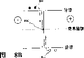
Fig. 8 (A) is present in can be with under Fig. 6 (C) state of specific region (or exist with bunch group) with high concentration to 8 (B) expression Ni element.Exactly, Fig. 8 (A) expression has being with of semiconductor silicon film of N type source/drain region and I type channel formation region.Fig. 8 (B) then represents being with of active layer of N channel-type thin-film transistor.
As shown in Fig. 6 (B) and 6 (C), the concentration of Ni element is partly concentrated, and the part is quite high, and high concentration partly is the form of silicide, so that it has significant impact to silicon fiml aspect electrical property.In this case, will form by the trap level 800 shown in caused Fig. 8 of silicide (A).If so, electronics 801 will combine with hole 802 through trap level.This phenomenon can make cut-off current increase, and mobility is reduced.
Fig. 8 (B) expression has being with of the caused I N-type semiconductor N of nickle silicide trap level.The state of Fig. 8 (B) this semiconductor of expression in electric field.In addition in this case, pass electronics 801 that conduction band moves and pass valence band and combine through the hole that trap level moves.This also is the phenomenon that the motion of the charge carrier that moves freely is slowed down, and also is simultaneously the reason that causes such as the characteristic variation of the semiconductor device of thin-film transistor etc.
Fig. 7 (A) is expression because the nickel acetate solution that is added with surfactant is coated onto the surface of amorphous silicon film 700, then is spin-dried for the figure of the state that is produced with spinner.In this state, owing to the effect of surfactant makes the surface active of amorphous silicon film 700, the Ni element just is adsorbed onto on the surface of amorphous silicon film 700, spreads out from the teeth outwards simultaneously.
Make it crystallization by in this state amorphous silicon film 700 being heat-treated, just reached the state of Fig. 7 (B).Exactly, Fig. 7 (B) expression makes it the state that crystallization obtains by the Ni element being distributed to silicon fiml 700 heat treatments in the silicon fiml.In this state, because the Ni element disperses existence, so can not form any silicide as the part of the scale forming current path.Therefore under the state of Fig. 7 (B), can not form the circuit pathways 602 shown in any for example Fig. 6 (C).If adopt the crystallization shape silicon fiml under Fig. 7 (B) state to make thin-film transistor, just can reduce cut-off current.
Utilize following example more at large to describe the present invention now, still, these examples are not to be used for limiting the scope of the invention.
The manufacture method of Fig. 1 (A)-1 (C) expression example 1 according to the present invention;
The manufacture method of Fig. 2 (A)-2 (D) expression example 2 according to the present invention;
The manufacture method of Fig. 3 (A)-3 (D) expression example 3 according to the present invention;
The manufacture method of Fig. 4 (A)-4 (D) expression example 4 according to the present invention;
The manufacture method of Fig. 5 (A)-5 (D) expression example 5 according to the present invention;
Fig. 6 (A)-6 (C) respectively is the figure that the nickel acetate solution that is illustrated in no surfactant is coated onto the state of nickel element under the situation on amorphous silicon film surface;
Fig. 7 (A) and 7 (B) respectively are the figures that the nickel acetate solution that is illustrated in surfactant is coated onto the state of nickel element under the situation on amorphous silicon film surface.
Fig. 8 (A)-8 (B) respectively represents the situation that silicon fiml can be with under the situation that nickel element cluster group exists.
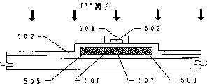
Example 1
This example is will prove in order to make the method for crystallization shape silicon fiml on glass substrate.At first as shown in Fig. 1 (A), utilize sputter or plasma CVD on healthy and free from worry (Corning) 7059 type glass substrate (deformation point is 593 ℃) or healthy and free from worry (Corning) 1737 type glass substrate (deformation point is 667 ℃) 101, to form the passivating film of the thick silicon oxide film 102 of 3000 .Silicon oxide film 102 is the diffusions that will prevent from the impurity of glass substrate.
Secondly, on silicon oxide film 102, form the thick amorphous silicon film 103 of 500 with known plasma CVD or decompression hot CVD method.Obtain state as shown in Fig. 1 (A) by this way.
Then, as as shown in Fig. 1 (B), sample is installed on the spinner 100, the nickel acetate solution of the Ni element that contains 10ppm weight is coated onto on the sample, this solution has added the surfactant of mainly being made up of higher alcohol type tween of 1% volume.
Just formed the liquid film 104 of this solution in this way.Then, the sample of coating like this is spin-dried for, thereby makes the Ni element keep contacting with amorphous silicon film 103 surfaces with spinner 100.
In above-mentioned steps, the nickel concentration in the available solution, liquid film 104 keep with the 103 contacted times of silicon fiml and are spin-dried for the concentration that situation control waits to introduce the Ni element in the amorphous silicon film 103.Especially, just can accurately control the concentration of the Ni element that finally is retained in the silicon fiml by the concentration that changes nickel in the solution.Be retained in Ni element in the silicon fiml concentration be preferably 1 * 10
16-5 * 10
19Cm
-3, 1 * 10
16-5 * 10
18Cm
-3Then better.This concentration of element is defined as the minimum that will be measured by SIMS (secondary ion mass spectrometry (SIMS) view).
After this, as shown in Fig. 1 (C), with amorphous silicon film 103 heating, modification becomes crystallization shape silicon fiml.This heat treatment is carried out in diffusion furnace.Heating condition is to carry out 4 hours under 550 ℃ of temperature.By heat treatment, obtain to finish crystalline form silicon fiml 105.Because 550 ℃ of temperature are lower than the deformation point (593 ℃) of healthy and free from worry 7059 type glass substrate, and heating time is short, so almost can ignore the distortion of substrate.On glass substrate 101, form in this way and finish crystalline form silicon fiml 105.In heat treatment process, the surfactant that is bonded on the amorphous silicon film 103 is evaporated, thereby can not cause any negative influence to acquisition crystallization shape silicon fiml 105.
Be in the temperature departure+/-1 ℃ or following scope in, heat or cool off that to carry out above-mentioned heat treatment in heating furnace be quite desirable with about 15 ℃/minute or following speed.This is because heating rapidly or cooling will cause the phase transformation from amorphous to crystallization shape, destroys uniform crystal growth, causes silicon fiml significantly to peel off and the silicon fiml be full of cracks from substrate.
According to present inventor's understanding, known with the speed more than 15 ℃/minute heating and cooling (especially heating) silicon fiml to make silicon fiml peel off and make the silicon fiml be full of cracks again and again, thereby reduced the practicality of silicon fiml significantly from substrate.
According to these viewpoints, wish that heater is not Fast Heating and the cooling device that for example adopts lamp annealing device (lamp-anneding device) etc., but can be the resistance heating device that can carry out accurate temperature control.
Before or after heat treatment, perhaps before and after the heat treatment, silicon fiml can be exposed under the laser beam.Especially it is quite useful making crystallization shape silicon fiml be subjected to laser beam lithography after heat treatment, because the amorphous composition that still is retained in the silicon fiml for heat treatment institute crystallization can so just can not obtain senior crystallization shape silicon fiml by the exposure crystallization.
Example 2
This example is to prove that utilization makes the method for thin-film transistor according to the crystal type silicon fiml 105 that method obtained of example 1.At first, the sample of preparation example as shown in Fig. 1 (C).Make the crystallization film have certain pattern, form the active layer 201 of thin-film transistor.As shown in Fig. 2 (A).
Secondly as shown in Fig. 2 (B), utilize plasma VCD form 1000 thick will be as the silicon oxide film 202 of gate insulating film.Then form the thick aluminium film that contains scandium of 6000 thereon, be processed into certain pattern then, form grid 203 by the electron beam vapor deposition.Grid 203 stands anodic oxidation in electrolyte, simultaneously it as anode, thereby form the thick alumina layer of 2000 204.Play mask in this alumina layer 204 foreign ion injection process afterwards, to form the compensation grid region.
Then, as shown in Fig. 2 (C), mix up by plasma and to carry out P
+The foreign ion of (phosphorus) ion injects.After mixing up operation, carry out the irradiation of KrF excimer laser ray, inject P thereby make
+The regional annealing of ion.Through after this processing, form source area 205, offset gate polar region 206, channel formation region 207 and drain region 208 with self-localization method.
Then, as shown in Fig. 2 (D), utilize plasma VCD to form the interlayer dielectric of the thick silicon oxide film of 7000 209.Form contact hole then, form source electrode 210 and drain electrode 211 with aluminium.At last, sample was heated one hour in 350 ℃ nitrogen atmosphere, just made thin-film transistor.
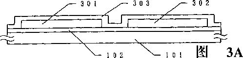
Example 3
This example is to prove that this transistor will be configured in the peripheral drive circuit district or the pixel circuit district of active-matrix liquid crystal display device in order to make the method for thin-film transistor on a substrate.At first as shown in Fig. 1 (C), on glass substrate 101, form crystallization shape silicon layer 105.Identical in the details of forming process and the example 1.Secondly as shown in Fig. 3 (A), sample is processed into certain pattern, forms active layer 301 and 302.Active layer 301 is used to constitute the thin-film transistor of peripheral circuit region, 302 thin-film transistors that are used to be disposed at pixel region of active layer.Then form 1000 , play the silicon oxide film 303 of gate insulating film effect with plasma CVD.
Then, utilize the electron beam vapor deposition to form the thick film of mainly forming of 6000 by aluminium.This film is processed into certain pattern, forms grid 304 and 305.These grids 304 and 305 are the process anodic oxidation in electrolyte, thereby all forms the thick oxide layer of 2000 306 and 307.In this way, reach the state shown in Fig. 3 (B).
Moreover, as shown in Fig. 3 (C), mix up with plasma and to carry out P
+The foreign ion of ion injects.Then sample is exposed under laser beam and the strong ray, forms source area 308 and 312, compensation grid region 309 and 313, channel formation region 310 and 314 and drain region 311 and 315 with self-localization method.
Then, utilize plasma CVD to form film between the insulating barrier of the thick silicon oxide film of 6000 316.So forming will be as the ITO electrode of pixel capacitors.Form contact hole, form source electrode 318 and 320 and drain 319 and 321 with aluminium.In this procedure, the drain electrode that be configured in the thin-film transistor in the pixel region is connected with the pixel capacitors 317 of ITO.In this way, make active-matrix liquid crystal display device.
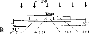
Example 4
This example is will prove a kind ofly optionally the Ni element to be introduced in a part of amorphous silicon film, becomes to give birth to the technology of crystal then along the direction that is parallel to silicon fiml from that part of beginning of introducing the Ni element.Fig. 4 A-4D represents the overview of the process of this example.
At first, utilize sputter or plasma CVD on glass substrate 101, to form the buffer film of the thick silicon oxide film 102 of 3000 .Secondly, on resilient coating, form the thick amorphous silicon film of 500 103 with plasma CVD or decompression hot CVD.
Moreover, form mask 401 with resist.The figure of this resist mask 401 is to make the surface of amorphous silicon film 103 come out with 402 zones of representing.Shape with the zone of 402 represented amorphous silicon film is along the quite long slit-shaped (seeing Fig. 4 (A)) of depth direction among the figure.
Then, as shown in Fig. 4 (B), sample is installed on the spinner 100,, has added the activator of mainly being formed of 1% volume in this solution by higher alcohol type tween with the nickel acetate solution coating that contains 10ppm weight Ni element.In this way, form liquid film 104.
Next with spinner 100 sample is spin-dried for, makes the Ni element keep directly contacting in view of the above with the surperficial of amorphous silicon film 103 of slit-shaped exposed region 402,
Remove resist 401 thereafter.Under this situation, the Ni element shown among Fig. 4 (C) 403 keeps directly contacting with exposed region 402 selectively.So sample is heated to 550 ℃, kept in this state 4 hours.This heat treatment cause along as with the crystal growth of the direction (promptly the edge is parallel to the direction of substrate) on 404 represented film surfaces.As being promoted that with post or needle-like mode crystal growth can reach more than the 100 μ m.
In this example, because surfactant has added the nickel acetate solution that the Ni element is disperseed, in crystal growing process, in fact the Ni element is distributed in the silicon fiml, thus the column of making or acicular crystal growth enrichment.As a result, can make the degree of crystallinity enrichment that will reach.
Therefore, as shown in Fig. 4 D, silicon fiml just has a zone along membrane plane direction generation crystal growth.Under the situation shown in Fig. 4 (D), the Ni element has been introduced along the zone 406 perpendicular to substrate 101 direction generation crystal growths.In zone 405, crystal growth is to take place along the direction that is parallel to substrate 101.Do not arrive zone 407 with 404 crystal growths of representing, therefore zone 407 still keeps amorphous.
Can introduce the metallic element of low concentration along the zone 405 that is parallel to substrate direction promotion crystal growth according to said method.If move on the border that a kind of like this structure that adopts charge carrier to move along crystal growth direction, charge carrier will crystal growths, thereby improved carrier mobility.
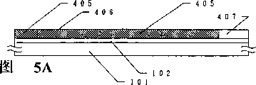
Example 5
This example is will prove a kind ofly to utilize crystal growth along the silicon fiml zone that the in-plane that is parallel to as the film that method obtained of example 4 takes place, the embodiment that forms thin-film transistor.At first, according to the method for Fig. 4 (A) to 4 (D), form crystal growth along being parallel to for example zone 405 (the seeing Fig. 5 (A)) that the substrate direction takes place.
The sample that is under Fig. 5 (A) situation is processed into has certain figure, thus the active layer that be used for thin-film transistor 501 of formation as shown in Fig. 5 (B).Importantly, the zone of formation active layer 501 is made of along the district 405 that the direction that is parallel to the silicon fiml plane takes place crystal growth.This is because the Ni element has directly been introduced zone 406, thereby higher concentration is wherein arranged.In addition, because in zone 406,, therefore, in zone 406, be lower than the mobility of charge carrier rate that moves in the zone 405 along being parallel to the mobility of charge carrier rate that the membrane plane direction moves along promoting crystal growth perpendicular to substrate 406 directions.
In the zone 405 direction of crystal growth almost be connected active layer on the direction of the source area that forms and the drain region route that will form identical also be quite important.Adopt this structure, can make the charge carrier that between source electrode and drain electrode, moves be subjected to the influence on crystal growth border hardly, thereby can improve the mobility of charge carrier rate.
Then, form the thick silicon oxide film that plays the gate insulating film effect 502 of 1000 with plasma CVD.Then, deposited by electron beam evaporation forms the thick film of mainly being made up of aluminium of 6000 .Next, sample is processed into has certain figure, form grid 503.Make it in electrolyte, stand anode treatment, and grid 503 as anode, thereby form the oxide layer 504 of 2000 .
With plasma mix up P thereafter,
+Ion injects sample, then with laser beam irradiation it is carried out annealing in process.Therefore, form source area 505, offset gate polar region 506, channel formation region 507 and drain region 508 (seeing Fig. 5 (C)) with self-localization method.
Next step forms film 509 between the insulating barrier of silicon oxide film 509 of 7000 .So after forming contact hole, form source electrode 510 and drain electrode 511 with aluminium.At last, sample is stood the heat of hydrogenation handle in 350 ℃ nitrogen atmosphere, made the thin-film transistor as shown in Fig. 5 (D).
According to the present invention of above detailed description, adopted the solution of the metallic element that can promote crystallization of silicon being introduced silicon fiml.Thereby can control the amount of the metallic element that will introduce simply.In addition, the silicon fiml of crystallization can have enough degree of crystallinity like this, simultaneously hardware is introduced silicon fiml and be can be controlled to such degree so that to the characteristic of semiconductor of silicon fiml without any negative influence.
According to the present invention, owing to can promote the metallic element of crystallization of silicon to keep contacting with discrete form with the amorphous silicon film surface of wanting silication.Be distributed to metallic element in the silicon fiml formation silicide that in the silicon fiml heat treatment process, can not gather together.
Metallic element is used for constituting under the situation of thin-film transistor with the crystallization shape silicon that above-mentioned discrete form exists therein, the few of silicide area that plays the local path effect of electric current of the transistor that is obtained, thereby, can suppress to flow through the path that produces by silicide area by (OFF) electric current.
Although with reference to embodiment the present invention has been done detailed description, obviously those skilled in the art can make various changes and correction under the premise without departing from the spirit and scope of the present invention.
Claims (39)
1. a method of making semiconductor device comprises the following steps:
On a glass substrate, form an amorphous silicon film;
The solution that will contain the metallic element that can promote crystallization of silicon is coated onto the surface of described amorphous silicon film; And
Thereby the amorphous silicon film heating with described metallic element is made its crystallization in the temperature range from 450 ℃ to this substrate distortion point,
Described method is characterised in that described solution comprises a kind of surfactant, and this surfactant comprises aliphatic carboxylic acid C
nH
2n+1COOH (wherein n representative is by 5 to 11 integer), and
Described surfactant evaporates by described heating.
2. a method of making semiconductor device comprises the following steps
On a glass substrate, form a silicon fiml;
The solution that will contain the metallic element that can promote crystallization of silicon is coated onto the surface of described silicon fiml, and
In the temperature range of deformation point from 450 ℃ to this substrate, the silicon fiml with described metallic element is heated,
Described method is characterised in that described solution comprises a kind of surfactant, and this surfactant comprises aliphatic carboxylic acid C
nH
2n+1COOH (wherein n representative is by 5 to 11 integer), and
Described surfactant evaporates by described heating.
3. a method of making semiconductor device comprises the following steps:
On a glass substrate, form an amorphous silicon film that comprises silicon;
Make one of described amorphous silicon film to select the surface to contact with a kind of solution that comprises the metallic element that can promote crystallization of silicon; And
Thereby the amorphous silicon film heating with described metallic element is made its crystallization in the temperature range from 450 ℃ to this substrate distortion point,
Described method is characterised in that described solution comprises a kind of surfactant, and this surfactant comprises aliphatic carboxylate C
nH
2n+1COONH
3R (wherein, n representative is by 5 to 11 integer, and R represents a hydrogen atom or have the alkyl of 5 to 10 carbon atoms), and
Described surfactant evaporates by described heating.
4. a method of making semiconductor device comprises the following steps:
On a tool glass substrate, form a silicon fiml;
Make one of described silicon fiml to select the surface to contact with a kind of solution that comprises the metallic element that can promote crystallization of silicon; And
In the temperature range of deformation point, to having the semiconductor film heating of described metallic element from 450 ℃ to this substrate;
Described method is characterised in that described solution comprises a kind of surfactant, and this surfactant comprises aliphatic carboxylate C
nH
2n+1COONH
3R (wherein, n representative is by 5 to 11 integer, and R represents a hydrogen atom or have the alkyl of 5 to 10 carbon atoms), and
Described surfactant evaporates by described heating.
5. a method of making semiconductor device comprises the following steps:
On a glass substrate, form an amorphous silicon film;
A surface of described amorphous silicon film is contacted with a kind of metallic element of crystallization of silicon that can promote, the effect by surfactant spreads out described metallic element, and
Thereby the amorphous silicon film heating with described metallic element and described surfactant is made its crystallization in the temperature range from 450 ℃ to substrate distortion point,
Described method is characterised in that described surfactant comprises aliphatic amine C
mH
2m+1NH
2(wherein m representative is by an integer of 7 to 14), and
Described surfactant evaporates by described heating.
6. a method of making semiconductor device comprises the following steps:
On a glass substrate, form a silicon fiml;
A surface of described silicon fiml is contacted with a kind of metallic element of crystallization of silicon that can promote, utilize the effect of surfactant and described metallic element is spread out; And
By 450 ℃ in the temperature range of the deformation point of this substrate, to having the silicon fiml heating of described metallic element and described surfactant;
Described method is characterised in that described surfactant comprises aliphatic amine C
mH
2m+1NH
2(wherein m representative is by an integer of 7 to 14), and
Described surfactant evaporates by described heating.
7. the method for device is partly led in a manufacturing, comprises the following steps:
On a glass substrate, form an amorphous silicon film;
The amorphous silicon film surface is contacted with the metallic element that can promote crystallization of silicon, and the described surface of this film is activated by surfactant simultaneously; And
Thereby the amorphous silicon film heating with described metallic element and described surfactant is made its crystallization in the temperature range from 450 ℃ to substrate distortion point,
Described method is characterised in that by making described surfactant and this metallic element adapted that described metallic element is distributed in the surface of silicon fiml, and
Described surfactant comprises aliphatic alcohol C
nH
2n+1OH (wherein n representative is by an integer of 6 to 12), and
Described surfactant evaporates by described heating.
8. a method of making semiconductor device comprises the following steps:
Silicon fiml of formation on a glass substrate '
The surface of described silicon fiml is contacted with the metallic element that can promote crystallization of silicon, and the described surface of this silicon fiml is activated by surfactant simultaneously; And
In temperature range, to having the semiconductor film heating of described metallic element and described surfactant by 450 ℃ of deformation points at the bottom of this substrate;
Described method is characterised in that by making described surfactant and this metallic element adapted, and described metallic element is distributed in the surface of silicon fiml,
Described surfactant comprises aliphatic alcohol C
nH
2n+1OH (wherein n representative is by an integer of 6 to 12), and
Described surfactant evaporates by described heating.
9. a method of making semiconductor device comprises the following steps:
On a glass substrate, form an amorphous silicon film;
Having under the situation of surfactant, can promote the metallic element of crystallization of silicon to introduce in the surface of described amorphous silicon film; And
Amorphous silicon film with described metallic element and described surfactant is heated, thereby makes its crystallization in temperature range from 450 ℃ to substrate distortion point,
Described method is characterised in that surfactant prevents metallic element local gathering in the silicon fiml surface,
Described surfactant mainly comprises a kind of higher alcohol type tween, and
Described surfactant evaporates by described heating.
10. a method of making semiconductor device comprises the following steps:
On a glass substrate, form a silicon fiml;
Having under the situation of surfactant, can promote the metallic element of crystallization of silicon to introduce in the surface of described silicon fiml, this surfactant mainly comprises higher alcohol type tween; And
By 450 ℃ in the temperature range of the deformation point of this substrate, to having the semiconductor film heating of described metallic element and described surfactant;
Described surfactant prevents metallic element local gathering in the silicon fiml surface,
Described surfactant evaporates by described heating.
11. the method according to the manufacturing semiconductor device of any one in the claim 1 to 10 is characterized in that: the described metallic element of crystallization of silicon that can promote comprises more than one that select from Fe, Co, Ni, Ru, Rh, Pd, Os, Ir, Pt, Cu and Au.
12. the method according to the manufacturing semiconductor device of any one in the claim 1 to 10 is characterized in that: describedly can promote that the metallic element of crystallization of silicon is Ni.
13. the method according to the manufacturing semiconductor device of any one in the claim 1 to 10 is characterized in that: after heating, the concentration of the metallic element that can promote crystallization of silicon that described silicon fiml is contained is 1 * 10
16Cm
-3To 5 * 10
19Cm
-3
14. the method according to the manufacturing semiconductor device of any one in the claim 1 to 10 is characterized in that: after heating, the content of the described metallic element that described silicon fiml is contained is 1 * 10
16Cm
-3To 5 * 10
18Cm
-3
15. the method according to the manufacturing semiconductor device of any one in the claim 1 to 10 is characterized in that: one of them is exposed in laser irradiation or the strong ray described film at least before described heating and afterwards.
16. method according to the manufacturing semiconductor device of any one in the claim 3 to 4, it is characterized in that: the metallic element that can promote crystallization of silicon is introduced the presumptive area of described silicon fiml, and reach along the direction that is parallel to described film by described heating and to adjoin the crystal growth of outer peripheral areas to it from this presumptive area.
17. according to the method for the manufacturing semiconductor device of any one in the claim 1 to 10, it is characterized in that: described metallic element is Ni; And more than one compounds that utilization is selected from nickelous bromide, nickel acetate, nickel oxalate, nickelous carbonate, nickel chloride, nickel iodide, nickel nitrate, nickelous sulfate, nickel formate, nickel acetylacetonate, 4-cyclohexyl butyric acid nickel, nickel oxide, nickel hydroxide and acetate nickel salt are introduced described film to described metal.
18. according to the method for the manufacturing manufacturing semiconductor device of any one in the claim 1 to 10, it is characterized in that: described metallic element is Fe, and utilizes from ferrous bromide (FeBr
26H
2O), ferric bromide (FeBr
36H
2O), ferric acetate (Fe (C
2H
3O
2)
3XH
2O), frerrous chloride (FeCl
24H
2O), iron chloride (FeCl
36H
2O), ferric flouride (FeF
33H
2O), ferric nitrate (Fe (NO
3)
39H
2O), ferrous phosphate (Fe
3(PO
4)
28H
2O) and ferric phosphate (FePO
42H
2O) more than one compounds of selecting in are introduced this film to above-mentioned metallic element.
19. according to the method for the manufacturing semiconductor device of any one in the claim 1 to 10, it is characterized in that: described metallic element is Co, and utilizes from cobaltous bromide (CoBr
26H
2O), cobalt acetate Co (C
2H
3O
2)
24H
2O), cobalt chloride (CoCl
26H
2O), cobaltous fluoride (CoF
2XH
2O) and cobalt nitrate (Co (No
3)
26H
2O) more than one compounds of selecting in are introduced described film to described metallic element.
20. according to the method for the manufacturing semiconductor device of any one in the claim 1 to 10, it is characterized in that: described metallic element is Ru, and utilizes ruthenic chloride (RuCl
3H
2O) described metallic element is introduced described film.
21. according to the method for the manufacturing semiconductor device of any one in the claim 1 to 10, it is characterized in that: described metallic element is Rh, and utilizes radium chloride (RhCl
33H
2O) described metallic element is introduced described film.
22. according to the method for the manufacturing semiconductor device of any one in the claim 1 to 10, it is characterized in that: described metallic element is Pd, and utilizes palladium bichloride (PdCl
22H
2O) described metallic element is introduced described film.
23. the method according to the manufacturing semiconductor device of any one in the claim 1 to 10 is characterized in that; Described metallic element is Os, and utilizes osmium chloride (OsCl
3) described metallic element is introduced described film.
24. according to the method for the manufacturing semiconductor device of any one in the claim 1 to 10, it is characterized in that: described metallic element is Ir, and utilizes from iridous chloride (IrCl
33H
2O) and iridic chloride (IrCl
3) in more than one compounds of selecting described metallic element is introduced described film.
25. according to the method for the manufacturing semiconductor device of any one in the claim 1 to 10, it is characterized in that: described metallic element is Pt, and utilizes platinum chloride (PtCl
45H
2O) described metallic element is introduced described film.
26. according to the method for the manufacturing semiconductor device of any one in the claim 1 to 10, it is characterized in that: described metallic element is Cu, and utilizes from copper acetate (Cu (CH
3OO)
2), copper chloride (CuCl
22H
2O) and copper nitrate (Cu (NO
3)
23H
2O) more than one compounds of selecting in are introduced described film to described metallic element.
27. according to the direction of the manufacturing semiconductor device of any one in the claim 1 to 10, it is characterized in that: described metallic element is Au, and utilizes from gold trichloride (AuCl
3XH
2O) and gold chloride (AuHCl
44H
2O) one or more compounds of selecting in are introduced described film to described metallic element.
28. a method of making semiconductor device comprises the following steps:
On a glass substrate, form a silicon fiml;
Prepare a kind of solution, it comprises a kind of material and a kind of surfactant that is used to promote described silicon fiml crystallization; And
Described solution is coated onto the surface of described amorphous silicon film,
In the temperature range of selecting to substrate distortion from 450 ℃, the described silicon fiml with described material and described surfactant is heated,
Described method is characterised in that described surfactant uses C from comprising
nH
2n+1The aliphatic carboxylic acid that COOH represents, use C
nH
2n+1COONH
3The aliphatic carboxylate that R represents, use C
mH
2m+1NH
2The expression aliphatic amine and use C
nH
2n+1Select in the group of the aliphatic alcohol that OH represents, and
Described surfactant evaporates by described heating.
29. according to the method for the manufacturing semiconductor device of claim 28, it is characterized in that: described surfactant comprises a hydrocarbon chain with 1 to 20 carbon atom as hydrophobic group.
30. the method according to the manufacturing semiconductor device of claim 28 further comprises the following steps:
Described silicon fiml is made the figure of a plurality of semiconductor islands; And
Place therebetween with grid and to form a plurality of grids that adjoin with described semiconductor island.
31. according to the method for the manufacturing semiconductor device of claim 28, it is characterized in that: the solvent of described solution is selected from polar solvent, polar solvent comprises water, alcohol, acid and amine.
32. according to the method for the manufacturing semiconductor device of claim 28, it is characterized in that: the solvent of described solution is selected from non-polar solven, non-polar solven comprises benzene,toluene,xylene, carbon tetrachloride and chloroform.
33. according to the method for the manufacturing semiconductor device of claim 28, it is characterized in that: described semiconductor device is an active-matrix liquid crystal display device.
34. want the method for 28 manufacturing semiconductor device according to right, it is characterized in that: more than one that select among described metallic element Fe, Co, Ni, Ru, Rh, Pd, Os, Ir, Pt, Cu and the Au.
35. the method according to the manufacturing semiconductor device of claim 28 is characterized in that, described surfactant adds described solution with 1% of volume.
36. the method according to the manufacturing semiconductor device of claim 28 is characterized in that further comprising such step: after described heating, with the described silicon fiml of laser irradiation.
37. the method according to the manufacturing semiconductor device of any one side in the claim 1 to 10 further comprises the following steps:
Described silicon fiml is made the figure of a plurality of semiconductor islands; And
Place therebetween with grid and to form a plurality of grids that adjoin with described semiconductor island.
38. according to the method for the manufacturing semiconductor device of any one in the claim 1 to 10, it is characterized in that: described semiconductor device is an active-matrix liquid crystal display device.
39. the method according to the manufacturing semiconductor device of any one in the claim 1 to 8 is characterized in that: surfactant prevents that the metallic element part from accumulating in the surface.
Applications Claiming Priority (2)
| Application Number | Priority Date | Filing Date | Title |
|---|---|---|---|
| JP331608/94 | 1994-12-09 | ||
| JP33160894A JP3418647B2 (en) | 1994-12-09 | 1994-12-09 | Semiconductor device manufacturing method and crystal growth promoter |
Publications (2)
| Publication Number | Publication Date |
|---|---|
| CN1132409A CN1132409A (en) | 1996-10-02 |
| CN1090813C true CN1090813C (en) | 2002-09-11 |
Family
ID=18245564
Family Applications (1)
| Application Number | Title | Priority Date | Filing Date |
|---|---|---|---|
| CN95121314A Expired - Fee Related CN1090813C (en) | 1994-12-09 | 1995-12-09 | Method for producing semiconductor devices, and crystal growth promoters |
Country Status (4)
| Country | Link |
|---|---|
| JP (1) | JP3418647B2 (en) |
| KR (1) | KR100444655B1 (en) |
| CN (1) | CN1090813C (en) |
| TW (1) | TW285778B (en) |
Families Citing this family (6)
| Publication number | Priority date | Publication date | Assignee | Title |
|---|---|---|---|---|
| KR0144643B1 (en) * | 1994-12-28 | 1998-08-17 | 심상철 | Fabrication method of polysilicon thin film by metal coating |
| JPH10228248A (en) | 1996-12-09 | 1998-08-25 | Semiconductor Energy Lab Co Ltd | Active matrix display device and its manufacture |
| US6794229B2 (en) | 2000-04-28 | 2004-09-21 | Semiconductor Energy Laboratory Co., Ltd. | Manufacturing method for semiconductor device |
| CN100337304C (en) * | 2003-08-22 | 2007-09-12 | 友达光电股份有限公司 | Method for forming polycrystalline silicon layer |
| JP2007108785A (en) * | 2006-12-25 | 2007-04-26 | Semiconductor Energy Lab Co Ltd | Semiconductor device |
| CN105632923B (en) * | 2014-10-28 | 2018-11-16 | 中芯国际集成电路制造(上海)有限公司 | The forming method of semiconductor structure |
Citations (2)
| Publication number | Priority date | Publication date | Assignee | Title |
|---|---|---|---|---|
| CN1090426A (en) * | 1992-12-04 | 1994-08-03 | 株式会社半导体能源研究所 | Semiconductor device and manufacture method thereof |
| EP0612102A2 (en) * | 1993-02-15 | 1994-08-24 | Semiconductor Energy Laboratory Co., Ltd. | Crystallized semiconductor layer, semiconductor device using the same and process for their fabrication |
-
1994
- 1994-12-09 JP JP33160894A patent/JP3418647B2/en not_active Expired - Fee Related
-
1995
- 1995-11-30 TW TW84112780A patent/TW285778B/zh not_active IP Right Cessation
- 1995-12-08 KR KR1019950047680A patent/KR100444655B1/en not_active IP Right Cessation
- 1995-12-09 CN CN95121314A patent/CN1090813C/en not_active Expired - Fee Related
Patent Citations (2)
| Publication number | Priority date | Publication date | Assignee | Title |
|---|---|---|---|---|
| CN1090426A (en) * | 1992-12-04 | 1994-08-03 | 株式会社半导体能源研究所 | Semiconductor device and manufacture method thereof |
| EP0612102A2 (en) * | 1993-02-15 | 1994-08-24 | Semiconductor Energy Laboratory Co., Ltd. | Crystallized semiconductor layer, semiconductor device using the same and process for their fabrication |
Also Published As
| Publication number | Publication date |
|---|---|
| JP3418647B2 (en) | 2003-06-23 |
| CN1132409A (en) | 1996-10-02 |
| TW285778B (en) | 1996-09-11 |
| JPH08167572A (en) | 1996-06-25 |
| KR100444655B1 (en) | 2004-11-26 |
Similar Documents
| Publication | Publication Date | Title |
|---|---|---|
| CN1143362C (en) | Method for manufacturing semiconductor device | |
| CN1052110C (en) | Semiconductor, semiconductor device, and method for fabricating the same | |
| CN1052565C (en) | A method for manufacturing a semiconductor device | |
| CN1078384C (en) | Method of fabricating semiconductor device | |
| CN1055786C (en) | Semiconductor device and method for its preparation | |
| CN1146955C (en) | Mfg. method for semiconductor device | |
| CN1079987C (en) | Method for producing semiconductor device | |
| CN1041148C (en) | A method and an apparatus for fabricating a semiconductor device | |
| CN1051877C (en) | Semiconductor device and method for producing the same | |
| CN1135608C (en) | Semiconductor device mfg. method | |
| CN1052567C (en) | A semiconductor device and a method of fabricating the same | |
| CN1156918C (en) | Semicondutor device | |
| CN1160759C (en) | Semiconductor device and its making method | |
| CN1218403C (en) | Semiconductor device and its producing method | |
| CN1320598C (en) | Manufacturing method of semiconductor device | |
| CN1109213A (en) | Method for producing semiconductor film and semiconductor device having the same | |
| CN1118521A (en) | Semiconductor device, method for producing the same, and liquid crystal display including the same | |
| CN1090813C (en) | Method for producing semiconductor devices, and crystal growth promoters | |
| CN1132928A (en) | Semiconductor device and method for fabricating the same | |
| CN1209792C (en) | Polysilicon semiconductor thin film substrate, method for producing the same, semiconductor device, and electronic device | |
| CN1149631C (en) | A method for manufacturing a semiconductor and an apparatus for the same |
Legal Events
| Date | Code | Title | Description |
|---|---|---|---|
| C06 | Publication | ||
| PB01 | Publication | ||
| C10 | Entry into substantive examination | ||
| SE01 | Entry into force of request for substantive examination | ||
| C14 | Grant of patent or utility model | ||
| GR01 | Patent grant | ||
| C17 | Cessation of patent right | ||
| CF01 | Termination of patent right due to non-payment of annual fee |
Granted publication date: 20020911 Termination date: 20121209 |