CN108873285B - High resolution scanning microscopy - Google Patents
High resolution scanning microscopy Download PDFInfo
- Publication number
- CN108873285B CN108873285B CN201810735160.9A CN201810735160A CN108873285B CN 108873285 B CN108873285 B CN 108873285B CN 201810735160 A CN201810735160 A CN 201810735160A CN 108873285 B CN108873285 B CN 108873285B
- Authority
- CN
- China
- Prior art keywords
- pixels
- detector array
- detection
- frame
- detector
- Prior art date
- Legal status (The legal status is an assumption and is not a legal conclusion. Google has not performed a legal analysis and makes no representation as to the accuracy of the status listed.)
- Active
Links
Images


Classifications
-
- G—PHYSICS
- G02—OPTICS
- G02B—OPTICAL ELEMENTS, SYSTEMS OR APPARATUS
- G02B21/00—Microscopes
- G02B21/0004—Microscopes specially adapted for specific applications
- G02B21/002—Scanning microscopes
- G02B21/0024—Confocal scanning microscopes (CSOMs) or confocal "macroscopes"; Accessories which are not restricted to use with CSOMs, e.g. sample holders
- G02B21/0052—Optical details of the image generation
- G02B21/0072—Optical details of the image generation details concerning resolution or correction, including general design of CSOM objectives
-
- G—PHYSICS
- G02—OPTICS
- G02B—OPTICAL ELEMENTS, SYSTEMS OR APPARATUS
- G02B21/00—Microscopes
- G02B21/0004—Microscopes specially adapted for specific applications
- G02B21/002—Scanning microscopes
- G02B21/0024—Confocal scanning microscopes (CSOMs) or confocal "macroscopes"; Accessories which are not restricted to use with CSOMs, e.g. sample holders
- G02B21/0052—Optical details of the image generation
- G02B21/0064—Optical details of the image generation multi-spectral or wavelength-selective arrangements, e.g. wavelength fan-out, chromatic profiling
-
- G—PHYSICS
- G02—OPTICS
- G02B—OPTICAL ELEMENTS, SYSTEMS OR APPARATUS
- G02B21/00—Microscopes
- G02B21/0004—Microscopes specially adapted for specific applications
- G02B21/002—Scanning microscopes
- G02B21/0024—Confocal scanning microscopes (CSOMs) or confocal "macroscopes"; Accessories which are not restricted to use with CSOMs, e.g. sample holders
- G02B21/008—Details of detection or image processing, including general computer control
-
- G—PHYSICS
- G02—OPTICS
- G02B—OPTICAL ELEMENTS, SYSTEMS OR APPARATUS
- G02B21/00—Microscopes
- G02B21/02—Objectives
- G02B21/025—Objectives with variable magnification
-
- G—PHYSICS
- G02—OPTICS
- G02B—OPTICAL ELEMENTS, SYSTEMS OR APPARATUS
- G02B21/00—Microscopes
- G02B21/18—Arrangements with more than one light path, e.g. for comparing two specimens
-
- G—PHYSICS
- G02—OPTICS
- G02B—OPTICAL ELEMENTS, SYSTEMS OR APPARATUS
- G02B21/00—Microscopes
- G02B21/36—Microscopes arranged for photographic purposes or projection purposes or digital imaging or video purposes including associated control and data processing arrangements
- G02B21/361—Optical details, e.g. image relay to the camera or image sensor
-
- G—PHYSICS
- G02—OPTICS
- G02B—OPTICAL ELEMENTS, SYSTEMS OR APPARATUS
- G02B6/00—Light guides; Structural details of arrangements comprising light guides and other optical elements, e.g. couplings
- G02B6/04—Light guides; Structural details of arrangements comprising light guides and other optical elements, e.g. couplings formed by bundles of fibres
- G02B6/06—Light guides; Structural details of arrangements comprising light guides and other optical elements, e.g. couplings formed by bundles of fibres the relative position of the fibres being the same at both ends, e.g. for transporting images
-
- G—PHYSICS
- G02—OPTICS
- G02B—OPTICAL ELEMENTS, SYSTEMS OR APPARATUS
- G02B26/00—Optical devices or arrangements for the control of light using movable or deformable optical elements
- G02B26/08—Optical devices or arrangements for the control of light using movable or deformable optical elements for controlling the direction of light
- G02B26/0816—Optical devices or arrangements for the control of light using movable or deformable optical elements for controlling the direction of light by means of one or more reflecting elements
- G02B26/0825—Optical devices or arrangements for the control of light using movable or deformable optical elements for controlling the direction of light by means of one or more reflecting elements the reflecting element being a flexible sheet or membrane, e.g. for varying the focus
-
- G—PHYSICS
- G02—OPTICS
- G02B—OPTICAL ELEMENTS, SYSTEMS OR APPARATUS
- G02B26/00—Optical devices or arrangements for the control of light using movable or deformable optical elements
- G02B26/08—Optical devices or arrangements for the control of light using movable or deformable optical elements for controlling the direction of light
- G02B26/0816—Optical devices or arrangements for the control of light using movable or deformable optical elements for controlling the direction of light by means of one or more reflecting elements
- G02B26/0833—Optical devices or arrangements for the control of light using movable or deformable optical elements for controlling the direction of light by means of one or more reflecting elements the reflecting element being a micromechanical device, e.g. a MEMS mirror, DMD
Abstract
The invention relates to a microscope and a method for high-resolution scanning microscopy of a sample, the sample being illuminated, a spot of light or a line of light guided scanningly through the sample being imaged as a frame, the spot being diffraction-limited to be imaged as a frame in an imaging ratio and the frame lying stationarily in a detection plane, the frame being detected for a scanning position with a position resolution which, taking into account the imaging ratio, is at least twice the half-value width of the diffraction-limited frame, the diffraction structures of the frame being thus detected, the diffraction structures of the frame being analyzed for each scanning position, an image of the sample being generated, the image having a resolution which exceeds the diffraction limit, a detector array being provided, the detector array having pixels and being larger than the frame, the radiation from the frame of the detection plane being redistributed nonimagically to the pixels of the detector array, redistribution elements being provided, the detection light being at least partially distinguished in terms of its spectral composition, the rays reach pixels of the detector array from the at least two redistribution elements.
Description
The application is a divisional application of an original application with the application date of 2014, 07, 18 and the national application number of 201480055894.2, and the invention name of high-resolution scanning microscopy.
The invention relates to a microscope for high-resolution scanning microscopy of a sample, comprising an illumination device for illuminating the sample, an imaging device for scanning at least one spot or line of light on the sample and for imaging the spot or line of light in an imaging scale as a diffraction-limited, stationary frame in a detection plane, a detector device for detecting the frames in the detection plane for different scanning positions with a position resolution which, taking into account the imaging scale, is at least twice the half-value width of the diffraction-limited frame, and an evaluation device for evaluating the diffraction structure of the frame for the scanning positions from the data of the detector device and for producing an image of the sample, the resolution of which exceeds the diffraction limit. The invention further relates to a method for high-resolution scanning microscopy of a sample, wherein the sample is illuminated, at least one point or line light spot guided scanningly on the sample is imaged as a frame, wherein the point or line light spot is imaged diffraction-limited to the imaging scale as a frame and the frame is stationary in the detection plane, the frame is detected for different scanning positions with a position resolution which, taking into account the imaging scale, is at least twice the half-value width of the diffraction-limited frame, so that the diffraction structures of the frame are detected, the diffraction structures of the frame are analyzed for each scanning position and an image of the sample is generated, the resolution of which exceeds the diffraction limit.
Such microscopic or microscopic methods are known, for example, from the publication Physical Review Letters,104,198101(2010) by C.M muller und j. enderlein, or from the patent document EP 2317362 a1, which also mentions further explanations regarding the prior art.
This achieves an increase in resolution by diffraction-limited imaging of the light spot on the detection plane. Diffraction limited imaging images a spot of light as an airy disk. The diffraction spot is detected in the detection plane in such a way that its structure can be resolved. Thus, the detector supersamples in terms of the imaging efficiency of the microscope. When the spot is imaged, the shape of the Airy spot is distinguished. Resolution enhancement of more than 2 times the diffraction limit is obtained by appropriate diffraction structure analysis, which is described in said document and the disclosure related thereto is fully included herein.
However, it is unavoidable in terms of detection that for each point on the sample that is scanned in this way, a frame must be recorded with a large amount of image information in comparison with a conventional laser scanning microscope (also referred to below as LSM). If the frame structure of one spot is detected, for example, in 16 pixels, each spot does not contain only 16 times the amount of data, but the single pixel on average contains only 1/16 of the intensity of the radiation impinging on the LSM detector in a typical pinhole detection. Since the radiation intensity is inevitably distributed unevenly over the structure of the frame, for example the airy disk, the radiation intensity at the structure edge is in fact even significantly smaller than the average value of 1/n for n pixels.
The problem to be solved is to be able to detect the amount of radiation at high resolution on the detector side. Conventional CCD arrays, which are typically used in microscopes, do not achieve a sufficient signal-to-noise ratio and therefore do nothing to do with even extending the image capturing time, which itself has been considered disadvantageous in applications. APD arrays are also associated with excessively high dark noise and therefore the signal-to-noise ratio obtained is not sufficient even if the measurement duration is extended. For CMOS detectors, it is also disadvantageous in terms of the size of the detector elements, since the diffraction limited frame of the light spot may fall on too few pixels. PMT arrays present similar structural space problems; the pixels at that point are too large as well. The installation space is therefore particularly problematic in that microscopes for high resolution can only be realized with the development effort, such as for example preparation equipment, if they can be integrated into existing LSM structures. Here, however, the determined size of the frame is preset. A large-area detector can only be installed if optics are additionally provided which again extend the image significantly, i.e. by a plurality of orders of magnitude. Such optics make it very costly to obtain diffraction-limited structures without other imaging errors.
Other methods are known in the prior art which avoid the problems in the detection at high resolution. A method is mentioned, for example, in EP 1157297B 1, in which the nonlinear processes are exploited by means of structured illumination. Structured illumination is pushed through the sample in multiple rotational and location positions and images the sample in these different states onto wide-field detectors for which the described limitations do not exist.
Methods for achieving high resolution (i.e. resolution of the image of the sample beyond the diffraction limit) without the limitations of the detector are also known from WO 2006127692 and DE 102006021317. The method, abbreviated PALM, uses a labeling substance which can be activated by means of an optical activation signal. The marking substance can only be excited by the excitation radiation in the activated state to emit certain fluorescent radiation; the unactivated molecules do not emit fluorescent radiation even in the presence of incident excitation radiation. The activating radiation brings the activating substance into a state in which it can be excited to emit light. It is often referred to as a transformed signal. The conversion signal is applied such that at least a proportion of the activated label molecules are spaced apart from adjacent, similarly activated label molecules, such that the activated label molecules are separated in terms of optical resolution of the microscopy or can be separated afterwards. This is called segregation of the activated molecules. For these isolated molecules, the center of their radiation distribution, which is obtained due to the limited resolution, can be determined simply and the position of the molecule can therefore be determined by calculation with a higher precision than what is really allowed by optical imaging. In order to image the entire sample, the PALM method exploits the fact that the probability that a marker molecule is activated by a transition signal at a given varying signal intensity is the same for all marker molecules. This applies the strength of the transformed signal so that the desired isolation is achieved. These method steps are repeated until as many as possible all of the marker molecules are contained once in the subset that has been excited to emit light.
In the present invention, the spot scanned on the sample is imaged stationary into the detection plane. The radiation from the detection plane is redistributed without imaging and directed onto the detector array. The term "unimageable" is used here with respect to the existing frames in the detection plane. Individual face regions of the frame may of course still be imaged according to the imaging theorem. Thus, between the detector array and the redistribution element are imaging optics. However, frames in the probe plane do not remain unchanged at the time of reassignment.
The term "diffraction-limited" is not limited to the diffraction limit according to the abbe principle, but also encompasses those cases in which the theoretical maximum is 20% less due to real inaccessibility or limitation. The frame also has a structure referred to herein as a diffractive structure at this time. It is oversampled.
This principle enables the use of a detector array that is not matched in size to the frame. The detector array is preferably larger or smaller in at least one extension than the frame to be detected. The concept of different geometric designs includes both different extensions of the detector array and different proportions of height and width relating to the extension of the frame in the detection plane. The pixels of the detector array may also be too large for the required resolution. This also allows that the outline of the pixel layout of the detector array is fundamentally different from the outline of the frame in the detection plane. Finally, the detector array has different dimensions in the detection plane than the frames according to the invention. The redistribution in the method or the redistribution elements in the microscope enable the detector array to be selected without regard to size limitations due to the frame and its size and pixel size limitations. In particular, detector rows can be used as detector arrays.
In LSM, the image of the sample is usually formed from a large number of frames, each assigned to a different scanning position, by scanning the sample with a light spot.
The solution according to the invention can also be carried out simultaneously for a plurality of spots in a parallelized form, as is known for laser scanning microscopes. Whereby a plurality of spots on the sample are scanned and the frames of the plurality of spots are stationary side by side in the detection plane. They are then redistributed by a common redistribution element of a size and area corresponding to the detector array or by a plurality of individual redistribution elements and are then directed onto a correspondingly larger individual or plurality of individual detector arrays.
The following exemplary focus describes scanning with one single spot. This is not to be understood as limiting, however, and the features and principles set forth are also applicable to the parallel scanning of a plurality of spot spots in nature and also to the case where line spots are applied. The latter is of course only diffraction-limited transversely to the line extension, so that the features relevant to this description apply only in one direction (transversely to the line extension).
By means of the method according to the invention, the ISM method can be carried out at satisfactory speed and with tolerable equipment expenditure. The invention opens up a wide, hitherto unformed field of application for the high-resolution microscopy principle.
The possibility of implementing a redistribution or redistribution element consists in using a bundle of optical fibres. The optical fibers can preferably be designed as multimode optical fibers. The beam has an entrance which is arranged in the detection plane and in its profile satisfies the extension of the diffraction-limited frame in the detection plane. While the optical fibres are arranged at the outlet in a geometrical layout preset by the detector array and this layout is different from the layout of the inlet. The exit-side end of the optical fiber can be guided directly to the pixels of the detector array. It is particularly advantageous to integrate the exit of the beam in a plug which can be conveniently inserted on a detector row, for example an APD or PMT row.
It is important for understanding the present invention to distinguish between pixels of the detector array and image pixels of the frame that are resolved in the detection plane. Each image pixel is typically assigned to exactly one detector array pixel, but the two differ in their layout. The main feature of the invention is that the rays of the supersampled image pixels, which make up the frame in terms of their size and layout, are taken in the detection plane. In this way, the structure of the frame is resolved, which is a diffractive structure due to the diffraction-limited generation of the frame. The redistribution element has an entrance side on which the image pixels are arranged. The entrance side is in the detection plane. A redistribution element directs radiation on each image pixel to a pixel of the detector array. The process of assigning image pixels to pixels of the detector array does not preserve the image structure and therefore the redistribution elements are not imaged with respect to the frame. The invention can also be characterized in that in a microscope of the type according to the invention, the detector arrangement has a non-imaging redistribution element with an entry side in the detection plane, at which entry side a ray with image pixels is recorded. The redistribution element also has an exit side, at which the radiation acquired at the image pixel is input into a pixel of the detector array, wherein the radiation is redistributed from the entrance side to the exit side without imaging relative to the frame. Similarly, the method according to the invention can be characterized in that, in a method of the type according to the invention, the radiation is recorded in a detection plane with image pixels, which are assigned to the pixels of the detector array without imaging relative to the frame. The detector array differs in the layout and/or size of its pixels from the layout and/or size of the image pixels in the detection plane. Furthermore, the image pixels in the detection plane are provided by the redistribution element in such a way that the diffraction structures of the frame are oversampled or oversampled with respect to the diffraction limit.
It is known for highly sensitive detector arrays that adjacent pixels exhibit interference due to crosstalk in the case of large differences in radiation intensity. To avoid this, an extended design is preferably used in which the optical fibers are guided from the inlet to the outlet in such a way that the optical fibers adjacent at the outlet are also adjacent at the inlet. Since diffraction-limited frames do not show jump-like radiation intensity variations, this design of the redistribution elements automatically ensures that the side-by-side pixels of the detector array have as small a radiation intensity difference as possible, which minimizes crosstalk or crosstalk.
Instead of a redistribution based on optical fibers, it is also possible to provide the redistribution elements with mirrors having mirror elements with different degrees of inclination. Such mirrors can be designed, for example, as segmented mirrors, as DMDs or as adaptive mirrors, wherein for the latter two variants a corresponding adjustment or control ensures the slope of the mirror element. The mirror elements direct radiation from the detection plane to pixels of the detector array, which have a different geometric layout than the mirror elements.
The mirror element displays the image pixels in terms of resolution of the diffractive structure of the frame, as do the ends of the optical fibers within the entrance of the optical fiber bundle. The size of the image pixels, and not (also) the pixel size of the detector array, is decisive for oversampling. A group of individual detectors is also understood here as a detector array, since their layout is always different (i.e. larger) than the image pixels in the detection plane.
For LSM, different objective lenses are used depending on the desired resolution. Switching of the objective lens changes the extension of the frame in the detection plane. It is therefore preferred that the zoom optics are arranged in front of the detection plane in the imaging direction for adapting the size of the frame to the size of the detector arrangement. Such a zoom optics changes the frame size in a percentage range of significantly less than 100%, i.e. much easier than the process of doubling the frame size as explained at the outset as a disadvantage.
The illumination of the sample is preferably performed as scanningly as in a normal LSM, even if it is not necessary. However, this achieves maximum resolution improvement. If the sample is illuminated scanningly, it is expedient if the illumination device and the imaging device have a common scanning device which guides the illumination spot through the sample and at the same time rescans (descannt) the spot coinciding with the illumination spot on which the sample is imaged relative to the detector, so that the frame is stationary in the detection plane. In this configuration, the zoom optics may be built into a common part of the illumination and imaging apparatus. This not only allows the adaptation of the frame to the size of the detector in the detection plane, but additionally also allows the usable illumination radiation to be incident completely into the objective aperture without edge losses, which may vary depending on the choice of objective.
The crosstalk between the adjacent pixels of the detector array, which is dependent on the radiation intensity, can be reduced in the redistribution by means of a suitable arrangement of the optical fibers in the bundle, as already mentioned at the outset. Additionally or alternatively, it is also possible to perform a calibration. For this purpose, each optical fiber is successively irradiated with radiation and interference signals in adjacent pixels are detected. In this way, a calibration matrix is created, by means of which the crosstalk of the side-by-side pixels, which is dependent on the radiation intensity, is corrected in the subsequent sample microscopy.
The resolution of the diffractive structure of the frame additionally allows the determination of the direction of motion of the light spot, along which it is moved when scanning the sample. Although the direction of movement is known in principle from the mechanical mechanism of the scanner (for example the scanning mirror or the movable sample stage), residual inaccuracies caused mechanically occur here. This can be eliminated by analyzing the signals of the individual pixels of the detector array by means of cross-correlation. This is used here to say that the side-by-side image pixels within the sample overlap to some extent due to diffraction-limited imaging of the light spot, but their centers are side-by-side. If the signals of these image pixels are analyzed with cross-correlation, the remaining inaccuracies that remain due to unavoidable tolerances of the scanning mechanical mechanism can be reduced or completely eliminated.
In addition to increasing the resolution, the temporal changes of the fluorescence in the detection volume detected by the light spots are detected by spatially and temporally correlating the signals consisting of the measurement sequences of the individual detector elements (assigned to the image pixels in the detection plane), for example the diffusion coefficients can be determined from the temporal correlation as in fluorescence correlation spectroscopy and the directional diffusion and diffusion barriers can also be visualized by taking into account the spatial correlation between the image pixels. The course of the movement of the fluorescent molecules is also of interest for tracking applications, since at this point the illumination spot should follow the movement of the fluorescent molecules. The arrangement described herein allows for highly accurate determination of the direction of motion during the pixel illumination time. It is therefore preferred as an extended design to detect changes within the sample by determining and analysing changes in the diffraction limited frame over time within a stationary spot of points or lines in the sample.
The method according to the invention also enables the illumination distribution to be modified in the case of scanning illumination, for example by means of a phase filter. The method can thus be implemented very simply, as described in opt.let.,34,3508(2009) of Gong et al.
Thus far, methods have been described in which a control unit carries out the method steps during operation of the microscope.
It goes without saying that the features mentioned above and those yet to be explained below can be used not only in the combination indicated, but also in other combinations or alone, without going beyond the scope of protection of the present invention.
The invention is further elucidated below, for example, on the basis of the appended drawings, which also disclose important features of the invention. In the drawings:
FIG. 1 shows a schematic diagram of a laser scanning microscope for high resolution microscopy;
FIG. 2 shows an enlarged view of the detector arrangement of the microscope of FIG. 1;
fig. 3 and 4 show a top view of a possible embodiment of the detector device 19 in the detection plane;
FIG. 5 shows an expanded design of the microscope of FIG. 1 with zoom optics for adapting the detector field size;
fig. 6 shows a variant of the microscope of fig. 5 with respect to the zoom optics and with respect to an extended design for multicolor imaging;
fig. 7 shows a variant of the microscope of fig. 1, wherein the variant relates to a detector arrangement;
fig. 8 shows a variant of the detector arrangement 19 of fig. 7;
FIG. 9 shows a laser scanning microscope arrangement for high-resolution observation of a sample in two different wavelength ranges by means of doubling of the detector and the fiber bundle;
FIG. 10 schematically illustrates a laser scanning microscope;
FIG. 11 shows a fiber arrangement for simultaneously taking images with improved resolution for two wavelength ranges;
fig. 12 shows a first solution for adapting the optics to different aperture sizes for two wavelength ranges to be detected;
fig. 13 shows a second solution for adapting the optics to different aperture sizes for two wavelength ranges to be detected;
fig. 14 shows a solution for adapting the optics to different aperture sizes for two wavelength ranges to be detected;
fig. 15 shows a variant of a laser scanning microscope;
FIG. 16 shows a sketch for the fiber layout of FIG. 15;
fig. 17 shows a further variant of a laser scanning microscope;
FIG. 18 shows a fiber arrangement for simultaneously taking images at improved resolution for two wavelength ranges and an additional alternative possibility for viewing a sample with finer Airy speckle sampling; and is
Fig. 19 shows a schematic diagram of a detection unit.
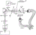
Fig. 1 schematically shows a laser scanning microscope 1, which is designed for microscopic observation of a sample 2. A laser scanning microscope (hereinafter abbreviated LSM)1 is controlled by a controller C and comprises an illumination beam path 3 and an imaging beam path 4. The illumination beam path illuminates a spot in the sample 2 and the imaging beam path 4 images the spot diffraction-limited for detection. The illumination optical path 3 and the imaging optical path 4 share a plurality of elements. But this is less necessary as is the case with scanning illumination of the sample 2. The sample may also be illuminated with a wide field.
The illumination of the sample 2 takes place in the LSM1 by means of the supplied laser radiation 5, which is incident on the mirror 8 via the deflecting mirror 6 and the lens 7, which do not need to be extensive in function. The mirror 8 is used to make the laser beam 5 incident on the emission filter 9 at a reflection angle. For a more intuitive display, only the main axis of the laser beam 5 is shown.
After reflection on the emission filter 9, the laser beam 5 is deflected biaxially by the scanner 10 and focused by means of lenses 11 and 12 via an objective 13 into a spot 14 in the sample 2. The light spot is shown here in the view of fig. 1 as a point, but may also be a line-shaped light spot. The fluorescent radiation excited in the spot 14 reaches the scanner 10 again via the objective 13 and the lenses 11 and 12, after which there is again a stationary light ray in the imaging direction. The light passes through emission filters 9 and 15, whose function is to select the fluorescence radiation in spot 14 in terms of wavelength and in particular to separate it from the illumination radiation of laser radiation 5, which can be used, for example, as excitation radiation. The lens 16 is used to image the spot 14 as a diffraction limited image in its entirety, which is in the detection plane 18. The detection plane 18 is a conjugate plane of the plane in which the spot 14 of the sample 2 lies. The image of the light spot 14 is recorded in a detection plane 18 by a detector device 19, which is explained further below with reference to fig. 2 to 4. What is important here is that the detector device 19 spatially resolves the diffraction-limited image of the light spot 14 in the detection plane 18.
The intensity distribution (gaussian distribution) of the light spot in the detection plane 18 over the detection cross-section is shown as 18a in fig. 1.
The controller C controls all components of the LSM1, in particular the scanner 10 and the detector arrangement 19. The controller takes the data of each frame 17 for different scan positions, analyses its diffraction structure and produces a high resolution overall image of the sample 2.
The LSM1 in fig. 1 is exemplarily shown for one unique light spot, which is scanned over the sample. However, the LSM1 may also be used simultaneously for scanning in line spots, which extend, for example, perpendicular to the drawing plane of fig. 1. It is also possible to design the LSM1 of fig. 1 such that multiple side-by-side spot spots in the sample are scanned. The corresponding frames 17 of the spot are also side by side in the detection plane 18. The detector arrangement 19 is correspondingly designed for detecting the side-by-side frames 17 in the detection plane 18.
The detector arrangement 19 is shown enlarged in fig. 2. The detector arrangement 19 consists of a fiber optic bundle 20, which feeds a detector array 24. The optical fiber bundle 20 is composed of a plurality of individual optical fibers 21. The end of the optical fibre 21 constitutes an optical fibre bundle inlet 22, which is located in the detection plane 18. The respective ends of the optical fibres 21 thus represent pixels by which diffraction-limited images of the spot 14 are taken. Since the light spot 14 is, for example, a point light spot in the embodiment of fig. 1, the image is an airy disk, which extends within the circle shown in fig. 1 and 2 of the detection plane 18. The extension of the bundle inlet 22 is of such a size that the extension of the airy disk is masked. The individual optical fibers 21 in the optical fiber bundle 20 are geometrically arranged at their outlet differently than at the optical fiber bundle inlet 22, i.e. in the form of an elongated plug 23, in which plug 23 the outlet-side ends of the optical fibers 21 are arranged side by side. The plug 23 is designed to be adapted to the geometric arrangement of the detector array, i.e. each outlet-side end of the optical fiber 21 is located directly in front of a pixel 25 of the detector array.
The geometric extent of the redistribution element is very basic, i.e. independent of its implementation, which in fig. 4 is implemented by a fiber bundle, adapted to the extent of the frame (or in the case of a plurality of spot spots of side-by-side frames) on the entry side. The function of the redistribution element is to record the radiation from the detection plane 18 in such a way that the intensity distribution of the frame is oversampled with respect to the diffraction limit as measured according to the scanning theorem, i.e. the redistribution element has pixels (formed by the entrance ends of the optical fibers in the configuration of fig. 3) which are situated in the detection plane 18 and which are at least 2 times smaller than the smallest resolvable structure which results from the diffraction limit taking into account the imaging scale in the detection plane 18.
Of course, the use of the plug 23 is only one of many possibilities to arrange the outlet side end of the optical fibre 21 before the pixel 25. It is equally feasible to use other connections. Individual pixels 25 may also be fused directly to the optical fibres 21. No detector rows need to be used; alternatively, a separate detector may be used for each pixel 25.
Fig. 3 and 4 show possible embodiments of the fiber bundle inlet 22. The optical fibers 21 may be fused to each other at the optical fiber bundle inlet 22. A higher space factor is thereby achieved, i.e. the space between the individual optical fibres 21 at the fibre bundle inlet 22 is minimised. Fusion on the other hand results in some degree of cross-talk between adjacent optical fibers. If it is desired to avoid this, the optical fibres may be bonded. It is also possible to arrange the ends of the optical fibres 21 in a square as shown in figure 4.
Preferably, the individual optical fibers 21 are assigned to individual pixels 25 of the detector array 24 in such a way that the optical fibers 21 lying next to one another at the fiber bundle inlet 22 are also next to one another at the detector array 24. In this way, crosstalk between adjacent pixels 25, which may occur, for example, as a result of scattered radiation or in the signal processing of individual pixels 25, is minimized. If the detector array 24 is a row, a corresponding arrangement can be achieved by determining the order of the individual optical fibers on the detector row by means of a spiral which connects the individual optical fibers one after the other in a plan view of the detection plane 18.
Fig. 3 also shows the dummy fibres 26 at the corners of the layout of the optical fibres 21 at the optical fibre bundle inlet 22. These non-effective fibers are not directed to the pixels 25 of the detector array. The signal intensity required for the signal analysis is no longer present at the position of the non-active fibre. The number of optical fibers 21 and thus the number of pixels 25 in a detector row or detector array can thereby be reduced to such an extent that, for example, operation is possible with 32 pixels. These detector rows are already used in other aspects of laser scanning microscopes, which has the advantage that the signal evaluation electronics need only be provided once in these laser scanning microscopes and it switches between the already existing detector rows and the other detector rows added by the detector arrangement 19.
According to fig. 4, optical fibers having a square basic shape are used for the bundle. The optical fiber also has a high coverage in the detection plane, i.e. effectively converges the radiation.
Fig. 5 shows an expanded design of the LSM1 of fig. 1, in which the zoom optics 27 are arranged in front of the detection plane 18. In the embodiment of fig. 1, the conjugate plane of the detection plane 18 forms an intermediate image plane 28, from which the zoom optics 27 record the radiation and guide it to the detection plane 18. The zoom optics 27 allow an optimal adaptation of the image to the entrance extension of the detector arrangement 19.
Fig. 6 shows a further variant of the laser scanning microscope 1 from fig. 1. On the one hand, the zoom optics are arranged here as zoom optics 29 such that they are in the partial beam path which is traversed by the illumination beam path 3 and the imaging beam path 4. This has the advantage that not only the size of the image can be adapted to the entrance side of the detector device 19, but also the aperture filling of the objective 13 and thus the degree of utilization of the laser beam 5 can be adapted relative to the imaging beam path 4.
Additionally in fig. 6, LSM1 is also designed as a two-channel system in that a beam splitter is arranged downstream of emission filter 9, which splits the radiation into two separate color channels. The corresponding elements of the color channels correspond to the elements arranged after the emission filter 9 in the imaging direction in LSM1 of fig. 1, respectively. Corresponding elements of the color channels are distinguished in the view of fig. 6 by the reference numeral suffixes "a" and "b", i.e., "15 a", "15 b", "16 a", "16 b", "17 a", "17 b", "18 a", "18 b", "19 a", and "19 b".
Of course, implementing two color channels is independent of using the zoom optics 29. The advantage of the combination is, however, that the zoom optics 27, which have to be arranged separately in both color channels and therefore repeatedly present, are only required once. However, the zoom optics 27 can of course also be used in the construction according to fig. 1 and the LSM1 of fig. 6 can also be realized without the zoom optics 29.
Fig. 7 shows a variant of the LSM1 of fig. 1 with regard to the detector arrangement 19.
The detector arrangement 19 has a segmented mirror 30 with individual facets 31. The prism surface 31 corresponds to the end of the optical fiber 21 at the fiber bundle inlet 22 in terms of the resolution of the image. The individual facets 31 differ in their slope with respect to the optical axis on which the radiation is incident. Together with a lens 32 and a miniature lens array 33 and a turning mirror 34 for ray folding only, each prism 31 images a face section of the frame 17 onto a pixel 25 of the detector array 24. Depending on the orientation of the facets 31, the detector array 24 may preferably be a 2D array here, but a detector row is also possible.
Fig. 8 shows an expanded design of the detector arrangement 19 of fig. 7, in which a refractive element 35 is also arranged upstream of the lens 32, which refractive element distributes the radiation particularly well to the detector rows.
As already mentioned, the detector array 24 may be chosen without further restrictions with regard to its geometry. Of course, the redistribution elements in the detector arrangement 19 have to be adapted to the respective detector array. Finally, the individual pixels of the resolved image are no longer preset in terms of their size by the detector array 24, but by elements which redistribute the radiation from the detection plane 18. In airy disc, the diameter of the disc is given in diffraction-limited imaging according to the formula 1.22 λ/NA, where λ is the mean wavelength of the imaged radiation and NA is the numerical aperture of the objective 13. The half width is 0.15. lambda./NA. In order to achieve high resolution, it is sufficient to design the position resolution at the time of detection to be twice the half-value width, i.e., to scan the half-value width twice. Thus, the maximum allowable width of the prism face 31 or the end of the optical fiber 21 at the optical fiber bundle inlet 22 is half the half-value width of the diffraction-limited frame. This of course applies in consideration of the imaging scale formed by the optics situated behind the objective 13. In the simplest case, a pixel array of 4x4 in the detection plane 18 per half-value width is sufficient.
The zoom optics described with reference to fig. 5 and 6, in addition to allowing such an adaptation that the diffraction profile of the diffraction-limited frame 17 of the spot 14 optimally fills the entrance area of the detector arrangement 19, also allows another way of operation when imaging more than one airy disk in the detection plane 18. In measurements where more than one airy disk is imaged on the detector device 19, light from other depth planes of the sample 2 is detected on the outer pixels of the detector device 19. Additional signal strength is obtained during processing of the image without affecting the depth resolution of the LSM 1. Thus, the zoom optics 27 or 29 allow a compromise to be made between depth resolution and the signal-to-noise ratio of the image.
The solutions shown in fig. 1-8 are suitable for obtaining data with improved spatial resolution for one wavelength range. However, for many applications it is desirable to obtain data in multiple wavelengths.
The disadvantage of continuous data acquisition is that, on the one hand, the acquisition time is more than doubled, since, in addition to the acquisition of the images, it also takes time to change the filters and to change the magnification of the image on the fiber bundle.
By doubling the detector arrangement and spectrally separating the signals by means of a dichroic beam splitter, time data for both wavelength ranges can be obtained (see fig. 9). However, sensitive detectors increase the cost of such devices. Furthermore, a computation unit for real-time data recording is required in addition to the additional detector. Finally, two real-time systems need to be controlled simultaneously. That is, this way of doubling the detection unit would bring about significant additional costs.
Fig. 9 shows a laser scanning microscope arrangement for high-resolution observation of samples in two different wavelength ranges by means of a doubling of the detector and the fiber bundle.
The color separator 40 separates the detection light path into two partial light paths having different wavelength ranges.
As already described above, adjustable focusing optics 41 and 42 are provided, respectively, as well as fiber bundles 43 and 44 and multi-channel detectors 45 and 46.
The object of the present invention is to avoid said disadvantages.
The invention is characterized by the features of the independent claims.
Preferred developments are the subject matter of the dependent claims.
The invention is explained in detail below, in particular with reference to the views in fig. 9 to 19.
Reference numerals of fig. 9-19 indicate:
40: color separator
41. 42: adjustable focusing optics
43. 44: fiber bundle
45. 46, 47: multi-channel detector
48. 49: fiber bundle
50. 51: detector region
52: adjustable focusing optics
53. 54: adjustable optical device
55: turnable steering mirror
56: fiber bundle
57. 58, 59: fiber bundle
60. 61, 62: detector region
63: optical demultiplexer/color filter
64. 65: fiber bundle
66. 67, 68: detector region
69: fiber bundle
70: multi-channel detector
71: color separator
72: mirror
The method according to the invention is based on the fact that two wavelength ranges can be detected by a single multi-channel detector, wherein a secondary airy disk scan of the sample signal can be carried out for both wavelength ranges.
As a detector in such an arrangement, as is described, for example, in DE102012204128a1, it is possible to use, for example, a GaAsP detector or a multi-channel detector consisting of 32 individual channels. When calculating high resolution images according to the method of Colin Shepard et al In Optik 80, No.2,53(1982), it is necessary to supersample the Airy spots at least twice In each spatial direction. For this reason, according to the invention, it is proposed to divide the, for example, 32 channels of the detector into two groups, i.e. 16 channels each. The 16 channels are each used to probe the sample signal by corresponding oversampling of the airy disk. The calculation of the 16 channel images for one wavelength range each results in a high resolution image.
In a laser scanning microscope arrangement, the sample signal is spectrally split into two optical paths, for example by means of a dichroic splitter (see fig. 9 for this purpose).
Fig. 10 schematically shows a laser scanning microscope, in which data for two wavelength ranges can be acquired simultaneously by only one detection unit. For this purpose, the sample light is spectrally separated by the color separator 40 and diverted on two fiber bundles 43, 44, which allow a secondary airy spot scan of the signal. The two fiber bundles then divert the light onto a common four-channel detector.
In this case, the imaging optics can image the sample plane onto two fiber bundles for two beam paths of the spectral range, which preferably each consist of 16 channels.
The sample plane is arranged optically conjugate with respect to the plane of the entrance surface of the fiber bundle. The respective fiber bundles conduct light of both wavelength ranges to a common detector. Such a fiber arrangement is schematically shown, for example, in fig. 11.
Fig. 11 shows a fiber arrangement for simultaneously capturing images with improved resolution for two wavelength ranges. In this case, the fibers 1 to 16 in the first plug or fiber bundle 48 (on the left in the drawing) are assigned to a first wavelength range; the fibers 17 to 32 in the second plug or fiber bundle 49 are assigned to a second wavelength range. The two plugs are in an image plane corresponding to the plane of the hole.
The fibers of the two plugs are then brought together in regions 50 and 51, respectively, on the multi-channel detector 47 (in the right part of the figure) in order to guide the light of the two wavelength ranges onto a common detector row with 32 channels.
In order to be able to ensure a stable reconstruction of high-resolution images on the basis of the two 16 detection channels, it is important, on the one hand, to correct for the crosstalk between the individual channels (both via the optical fibers and on or in the detector). This can be done, for example, by calibration measurements, in which a defined amount of light is introduced into each fibre in turn and the signals on all channels are measured. The matrix thus obtained can be reversed in order to assign the intensity distribution on the fibre to the signal measured on the detector.
On the other hand, it must be ensured that the fibers are arranged in two fiber bundles 48, 49 in such a way that a secondary sampling of the airy disk is ensured. The layout shown in fig. 11 is based on a hexagonal layout of round fibers. For the horizontal direction, airy disc can be detected by the fibers 13, 2, 1, 5 and 16. At 60 ° angles to them are fibers 14, 3, 1, 6 and 11; at 120 ° angles are fibers 15, 4,1, 7 and 12. In this way the scanning rule described above is implemented for three orientations. The additional fibers 8, 9 and 10 improve the collection efficiency and thus the signal-to-noise ratio on the one hand and the sampling for the remaining orientations on the other hand.
The described fiber arrangement is not limited to such fiber arrangements with circular diameters; this arrangement can also be specified for hexagonal fibers. This arrangement is also possible for square fibres, which in this case are provided in a square matrix of 4x4 elements. In this case, sampling of 4 fibers for different directions of the airy disk is achieved.
When observing an object through a microscope in a plurality of wavelengths, it is noted that the size of the airy disk depends on the wavelength. The size of the airy disk is proportional to the wavelength. Therefore, in order to optimally sample the airy disk, the imaging needs to be adapted to the fibers for the two wavelength ranges. For this purpose, there are several solutions according to the invention:
one adjustable focusing optic 41, 42 is used for each of the two optical paths in order to achieve optimal sampling for both regions (see also fig. 12). This layout is characterized by maximum flexibility.
Fig. 12 shows a first solution for adapting the optics to different aperture sizes for two wavelength ranges to be detected. In this case, the two detection channels each have a respective adjustable focusing optics 41, 42. This solution allows maximum flexibility.
Alternatively, it is possible to use a part of the scaling system jointly for both wavelength ranges. The optical path assignment is performed after the common use portion of the adjustable focusing optics 52 (see also fig. 13). This layout is similar to the flexibility of the first solution, but it is less costly and more compact.
Fig. 13 shows a second solution for adapting the optics to different aperture sizes for the two wavelength ranges to be detected. In this case, both detection channels have common adjustable focusing optics 52; the adaptation to the hole size is then effected in separate light paths by adjustable optics 53, 54 which are movable along the optical axis.
The flexibility of this solution is similar to the solution described previously in fig. 12.
There are usually typical combinations of wavelength ranges that should be measured simultaneously. This is derived from the typical combination of pigments used to stain biological samples. If the relationship of the center wavelengths for a typical combination is observed, the value λ is derived1/λ21.15. This proportional relationship can be used to further simplify the optical system:
the wavelength separation of the detection light is carried out as shown in fig. 13 after the commonly used adjustable focusing optics 52. The imaging of the longer-wavelength detection channel is then reduced by a factor of, for example, approximately 1.15, so that the airy disk is equal in size on both fiber bundles for both wavelength ranges (see also fig. 13).
Alternatively, fibers are used in both fiber bundles whose diameters (and also their bundle diameters) exactly have a relationship of, for example, 1.15 (see fig. 14). In this way no additional optics may be used in one of the two detection channels.
Fig. 14 shows such a solution for adapting the optics to different aperture sizes for the two wavelength ranges to be detected. In this case, both detection channels have common adjustable focusing optics 52. Adaptation to the pore size is achieved by varying the fiber diameter and the fiber bundle diameter in 43, 44; they have a fixed proportional relationship with each other corresponding to a typical wavelength relationship.
Finally, the possibility also exists of not using additional optics and different fiber diameters. In this case, it is proposed either to select the best sampling for one wavelength range while confirming that the scanning for the second wavelength range is worse, or to adjust the scaling such that the airy disk is about 7.5% too large on one fiber bundle and too small on the second fiber bundle. This effect can be taken into account in the reconstruction, but does not lead to an optimal resolution increase.
Alternatively, the adjustable focusing optics are designed such that they have lateral chromatic aberrations which exactly cancel out the enlargement of the airy disk.
In all the described arrangements, the color separator can be replaced by a corresponding mechanical mechanism, so that the selection of the two wavelength bands can be made more flexible.
In principle, the aforementioned arrangements and variants can also be extended to more than two wavelength ranges. For this purpose, additional color and detector channel assignment is required.
Fig. 15 shows a variant of a laser scanning microscope, in which data for two wavelength ranges can be acquired simultaneously by means of the fiber bundles 43, 44 with a single detection unit, and in which measurements at one wavelength can alternatively be carried out by means of the fiber bundle 56 (depending on whether the tiltable mirror 55 is in the beam path). All three fiber bundles allow for a secondary airy disk scan of the signal. The signals are then diverted to a common multi-channel detector.
Fig. 16 shows a sketch for the fiber layout of fig. 15 for simultaneous image capture with increased resolution for two wavelength ranges, and as a complementary alternative possibility, samples can be observed with finer airy disc sampling or improved signal-to-noise ratio (SNR) depending on the size of the airy disc at the fiber entrance. In this case, the fibers 1 to 16 in the first plug or fiber bundle 57 (43 in fig. 15) are assigned to a first wavelength range on the multi-channel probe 47; the fibers 17 to 32 in the second plug or fiber bundle 59 (44 in fig. 15) are assigned to a second wavelength range. An electrical plug or fiber bundle 59 (56 in fig. 15) having fibers 1 'to 32' is used to alternatively view the sample at one wavelength through the total detection face of the multi-channel detector 47.
All three plugs lie in one image plane. The fibers of all three plugs are then brought together (in the right part of the figure) in order to guide the light of the two wavelength ranges to a common detector row with 32 channels. In this case, the collection is carried out in such a way that 1 'of the fibers 1 and 59 in 57 is assigned to the first detector channel, the fibers 2 and 2' to the second channel, and so on. In this way, measurements can be made selectively in two wavelengths with the same detector or in one wavelength but with finer sampling or improved signal-to-noise ratio.
Fig. 17 shows a further variant of a laser scanning microscope, in which data for two wavelength ranges can be acquired simultaneously by only one detection unit, and in which measurement can alternatively be carried out in one wavelength (depending on whether a movable color separator is in the beam path). All two fiber bundles 43, 44 allow a secondary airy spot scan of the signal. The signals are then diverted to a common multi-channel detector 47. If detection is required for only one wavelength, light from the fiber bundle 1 can be prevented from impinging on the detector by means of a fold-in or movable light filter or color filter 63. Instead, it is possible to use a light filter or color filter 63 (with different transmission properties) so that, when viewing the two wavelength ranges, no light from the fiber bundle 2 impinges on the detector channel illuminated by the fiber bundle 1.
Fig. 18 shows a fiber arrangement for simultaneously taking images at improved resolution for two wavelength ranges, and an additional alternative possibility for observing a sample by finer airy disc sampling. In this case, the fibers 17 to 32 in the first plug (in the left part of the drawing) are assigned to a first wavelength range on the multi-channel probe 47; the fibers 1 to 16 in the second plug are assigned to a second wavelength range on the multi-channel probe 47. Alternatively, the total sample light may be diverted in fig. 12 only to the second plug, e.g. by flipping of the color separator; fibers 1 'to 32' (detector region 68) are used to capture data at one wavelength. The two plugs are in an image plane optically conjugate to the sample plane. The fibers of the two plugs are then brought together (in the right part of the figure) in order to guide the light of the two wavelength ranges to a common detector row with 32 channels. Here, the integration is carried out in such a way that the fibers 17 and 17 'of the fibers 17 and 65 in 64 are assigned to the seventeenth detector channel, the fibers 18 and 18' to the eighteenth channel and so on; the front sixteen detector channels receive signals only through the fibers 1 'to 16'. In this way, it is possible to selectively measure in two wavelengths by means of the same detector or in one wavelength but with finer sampling or improved signal-to-noise ratios.
Fig. 19 shows a schematic diagram of a detection unit for detecting high resolution images for two color channels. Here, the color separation is performed after the fiber bundle 69.
A miniaturized color splitter 71 is installed upstream of the detector matrix or detector row, which respectively loads the detector elements in transmission and the second detector element by double reflection on the splitter mirror and a further mirror 72.
The signal is split into two spectral portions by means of a color splitter 71 and a mirror 72 and distributed to the two detector elements of the multi-channel detector 70. In this example, for example, a high resolution image for a first wavelength range is generated from odd-numbered detector channels and an image for a second wavelength range is generated from even-numbered detector channels.
The variant comprises the following steps:
the following describes different variants of the aforementioned solution according to the invention:
a) if the sensitive surface of the multi-channel detector used is large enough, the fiber bundles can be arranged such that more than one fiber bundle guides the line onto the detector element. In this way, the user may use the detection channel for simultaneous detection of two wavelength ranges as described above, or alternatively provide all detector channels for observing the sample in one wavelength within the second detection channel (e.g., based on observation of more than one airy disk with finer airy disk sampling or improved signal-to-noise ratio). This combined fibre plug layout is shown in the drawings.
b) As an alternative to the above solution, 16 fibers are grouped together in one of the two fiber bundles, while 32 fibers are included in the second fiber bundle. A schematic view of this is shown in fig. 17. The observation of the sample in the two wavelength ranges can also be realized here. For the first wavelength range, fibers 1 'and 16' from a fiber bundle with 32 fibers were used, and fibers 16 to 32 from a fiber bundle with 16 fibers were used for the second wavelength range (see fig. 17).
In this case, in order to ensure that the sample light does not impinge on the detector from the fibers 17 'to 32' when detecting data at both wavelength ranges, it is necessary to incorporate a wave splitter between the fiber exit 17 'to 32' and the detector channels 17 to 32 entering the light path, or to insert a color filter between the fiber end 17, 17 ', … 32, 32' and the corresponding detector channel, which color filter transmits only light of the wavelength range of the fibers 17 to 32 and blocks light from the fibers 17 'to 32'.
c) Another alternative to the foregoing arrangement is based on the use of individual fiber bundles. The spectral separation of the wavelength range is only carried out between the fiber exit and the detector. In this case, beam splitting is carried out after each fiber, corresponding to the wavelength band. The two wavelength bands are then distributed over the two detector elements. The view is shown in fig. 19. It should be noted that the fiber bundle can be adapted to one wavelength or to a compromise between two wavelengths. The adjustable focusing optics are alternatively designed such that they have lateral chromatic aberrations which exactly compensate for the increase in the airy disk. Additional focusing optics are required as necessary to orient the fiber light in alignment with the detector channels.
d) In a further alternative arrangement, two fiber bundles are used, wherein the microscope-side fiber plugs are arranged side by side. One focusing optic satisfies the function of arranging two wavelength bands side by side. This function is produced by an optical element with variable axial lateral chromatic aberration. This can be achieved, for example, by a wedge K with a higher degree of dispersion (arranged in fig. 9, for example, before the adjustable focusing optics 41), which can be moved perpendicular to the optical axis. In this way, light in the first wavelength range is diverted to the fibers 1 to 16, while light in the second wavelength range reaches the fibers 17 to 32 spatially offset. The selection of the wavelength range can be achieved by different wedge angles (a "stepped" wedge or a switchable wedge with different wedge angles, which is moved in the optical path).
Alternatively, the variable axial transverse chromatic aberration can be realized by a laterally displaceable lens section KG, which is arranged in fig. 9 as an example behind the adjustable focusing optics 41, the refractive index and the abbe number of which are selected such that the two wavelength ranges are spatially separated. By moving the wedge in the optical path, a range of wavelengths can be selected. Such an element is known from DE19951482a 1.
In both cases, additional mirrors known in the art may optionally be required in order to divert the light of the two spatially separated wavelength ranges onto the two fiber bundles.
Claims (37)
1. A microscope for high-resolution scanning microscopy of a sample (2) has
-illumination means (3) for illuminating the sample (2),
-imaging means (4) for scanning at least one spot of point or line light (14) on the sample (2) and for imaging the spot or line light (14) in an imaging scale as a diffraction-limited stationary frame (17) in a detection plane (18),
a detector device (19) for detecting the frames (17) in the detection plane (18) with a position resolution for the different scanning positions, which position resolution is at least twice the half-value width of the diffraction-limited frame (17) in at least one extension/dimension, taking into account the imaging scale,
-analysis means (C) for analyzing the diffraction structure of the frame (17) for the scan position from the data of the detector means (19) and for generating an image of the sample (2) with a resolution exceeding the diffraction limit, wherein,
-the detector arrangement (19) has:
-a detector array (24) having pixels (25) and being larger than the frame (17), and
a non-imaging redistribution element (20-21; 30-34; 30-35) which is arranged in front of the detector array (24) and distributes the radiation from the detection plane (18) non-imagewise onto pixels (25) of the detector array (24),
-wherein at least two redistribution elements are provided which are simultaneously loaded by the detection light, and wherein the detection light at least partially differs in its spectral composition and the radiation reaches the pixels of the detector array from the at least two redistribution elements,
-wherein at least one color separator is arranged in the detection beam path for generating at least two partial beam paths having at least partially different spectral characteristics,
-wherein each of said redistribution elements is a fiber bundle, the fiber ends of which terminate at a pixel of the detector array.
2. A microscope as claimed in claim 1, characterised in that the redistribution element comprises a bundle (20) of optical fibres (21) having an entrance (22) and an exit (23) arranged in the detection plane (18), the optical fibres (21) terminating at the exit (23) at pixels (25) of the detector array (24) in a geometrical layout different from the entrance (22).
3. The microscope of claim 2 wherein said optical fiber is a multimode optical fiber.
4. A microscope according to claim 2 or 3 wherein the optical fibres extend from the entrance (22) to the exit (23) such that adjacent optical fibres (21) at the exit (23) are also adjacent at the entrance (22) to minimise radiation intensity dependent cross-talk of side by side pixels (25).
5. A microscope as claimed in claim 1 wherein the redistribution elements comprise mirrors (30) with mirror elements (31) of different inclinations which divert radiation from the detection plane (18) onto pixels (25) of the detector array (24), wherein the pixels (25) of the detector array (24) have a different geometrical layout than the mirror elements (31).
6. A microscope as claimed in claim 1, characterized in that the imaging device (4) has a zoom optics (27) arranged in the imaging direction in front of the detection plane (18) for adapting the size of the frame (17) to the size of the detector device (19).
7. A microscope as claimed in claim 6, characterized in that the illumination device (3) and the imaging device (4) share a scanning device (10) such that the illumination device (3) illuminates the specimen (2) to form a diffraction-limited spot of point or line light (14) thereon, which spot or line light (14) coincides with the spot imaged by the imaging device, wherein the zoom optics (27) are arranged such that they are also part of the illumination device (3).
8. A microscope as claimed in claim 1 characterised in that the detector array (24) is a detector row.
9. The microscope of claim 8 wherein said detector array is an APD or PMT array.
10. A microscope according to claim 5 characterised in that the mirror (30) is a segmented mirror, DMD or adaptive mirror.
11. The microscope of claim 1 wherein the probe light passes from the redistribution element to an adjacent region of the detector array.
12. The microscope of claim 1 wherein at least one pixel of the detector array is loaded with detection light from at least two redistribution elements.
13. A microscope as claimed in claim 1, characterized in that the pixels of the detector array are loaded both with filtered spectrally composed detection light and with spectrally unfiltered detection light.
14. A microscope as claimed in claim 1, characterized in that for spectrally filterless detection more pixels are loaded with detection light than for spectrally filtered detection.
15. A microscope according to claim 14 wherein the pixels subjected to said loading are arranged side by side and/or are loaded with light from at least two redistribution elements.
16. A microscope as claimed in claim 1, characterized in that a switching element is arranged in the detection beam path for initiating the application of the redistribution element by means of the unfiltered detection beam.
17. The microscope of claim 1 wherein at least two fibers of different fiber bundles terminate at a pixel of the detector array.
18. A microscope as claimed in claim 1, characterized in that the dichroic mirror and the deflection element are arranged in the direction of the light rays after the light conductor and before the pixels of the detector array in such a way that adjacent detection pixels are loaded with at least partially different wavelengths.
19. A method for high resolution scanning microscopy of a sample (2), wherein,
-illuminating the sample (2),
imaging at least one point or line spot (14) guided scanningly on the sample (2) as a frame (17), wherein the point or line spot (14) is imaged diffraction-limited to the imaging scale as a frame (17) and the frame (17) is stationary in a detection plane (18),
-detecting the frames (17) with a positional resolution for the different scanning positions, which positional resolution is at least twice the half-value width of the diffraction-limited frames (17) taking into account the imaging scale, thereby detecting the diffractive structure of the frames (17),
-analyzing the diffractive structure of the frame (17) and generating an image of the sample (2) for each scan position, the resolution of the image exceeding the diffraction limit, wherein,
-providing a detector array (24) having pixels (25) and being larger than the frame (17), and
-rays from a frame of the detection plane (18) are redistributed imagewise onto pixels (25) of the detector array (24),
-wherein at least two redistribution elements are provided which are simultaneously loaded by the detection light, and wherein the detection light at least partially differs in its spectral composition and the radiation reaches the pixels of the detector array from the at least two redistribution elements,
-wherein at least one color separator is arranged in the detection beam path for generating at least two partial beam paths having at least partially different spectral characteristics,
-wherein each of said redistribution elements is a fiber bundle, the fiber ends of which terminate at a pixel of the detector array.
20. Method according to claim 19, characterized in that the radiation of the frame (17) is redistributed by means of a bundle (20) of optical fibres (21), said bundle having an entrance (22) and an exit (23) arranged in the detection plane (18), the optical fibres (21) ending at the exit (23) at pixels (25) of the detector array (24) in a geometrical layout different from the entrance (22).
21. The method of claim 20 wherein said optical fiber is a multimode optical fiber.
22. A method as claimed in claim 20 or 21, characterized in that the optical fibres (21) are guided from the inlet (22) to the outlet (23) in such a way that optical fibres (21) adjacent at the outlet (23) are also adjacent at the inlet (22) in order to minimize radiation intensity-dependent crosstalk of side-by-side pixels (25).
23. Method according to claim 19, 20 or 21, characterized in that the bundle (20) of optical fibers (21) and the detector array (24) are calibrated by individually loading each optical fiber (21) with radiation, detecting interference signals in pixels (25) assigned to adjacent optical fibers (21) at the exit opening (23) and establishing a calibration matrix by means of which the radiation intensity-dependent crosstalk of side-by-side pixels (25) is corrected in microscopy of the sample (2).
24. Method according to claim 19, characterized in that the radiation of the frame (17) is redistributed by means of mirrors with mirror elements having different degrees of inclination, wherein the radiation from the detection plane (18) is directed by means of mirrors to the pixels (25) of the detector array (24), and the pixels (25) of the detector array (24) have a different geometrical layout than the mirror elements.
25. The method of claim 19, wherein said detector array (24) is a detector row.
26. The method of claim 25 wherein said detector array is an APD or PMT array.
27. Method according to claim 19, characterized in that the direction of movement of the scanning of the spot or line spot (14) is determined by analyzing the signals of the individual pixels (25) of the detector array (24) by means of cross correlation.
28. Method according to claim 19, characterized in that the change in the sample (2) is detected by determining and analyzing the change over time of the diffraction limited frame (17) for a spot of points or a line spot (14) stationary in the sample (2).
29. The method of claim 24, wherein said mirror (30) is a segmented mirror, a DMD, or an adaptive mirror.
30. The method of claim 28 wherein the probe light passes from the redistribution element to an adjacent region of the detector array.
31. The method of claim 28, wherein at least one pixel of the detector array is loaded with the detection light from the at least two redistribution elements.
32. The method of claim 20, wherein the pixels of the detector array are loaded with both filtered spectrally composed detection light and spectrally unfiltered detection light.
33. The method of claim 20, wherein for detection without spectral filtering more pixels are loaded with detection light than for detection with spectral filtering.
34. A method according to claim 33, wherein the pixels subjected to said loading are arranged side by side and/or the pixels are loaded with light from at least two redistribution elements.
35. The method of claim 20, wherein a switching element is provided in the detection beam path for initiating the loading of the redistribution element with the unfiltered detection beam.
36. The method of claim 20, wherein at least two fibers of different fiber bundles terminate at a pixel of the detector array.
37. A method as claimed in claim 20, characterized in that dichroic mirrors and turning elements are arranged in the direction of the light rays after the light conductor and before the pixels of the detector array in such a way that adjacent detection pixels are loaded with at least partially different wavelengths.
Applications Claiming Priority (5)
| Application Number | Priority Date | Filing Date | Title |
|---|---|---|---|
| DE102013013793 | 2013-08-15 | ||
| DE102013013793.4 | 2013-08-15 | ||
| DE201310019348 DE102013019348A1 (en) | 2013-08-15 | 2013-11-15 | High-resolution scanning microscopy |
| DE102013019348.6 | 2013-11-15 | ||
| CN201480055894.2A CN105612454A (en) | 2013-08-15 | 2014-07-18 | High-resolution scanning microscopy |
Related Parent Applications (1)
| Application Number | Title | Priority Date | Filing Date |
|---|---|---|---|
| CN201480055894.2A Division CN105612454A (en) | 2013-08-15 | 2014-07-18 | High-resolution scanning microscopy |
Publications (2)
| Publication Number | Publication Date |
|---|---|
| CN108873285A CN108873285A (en) | 2018-11-23 |
| CN108873285B true CN108873285B (en) | 2020-11-24 |
Family
ID=52430067
Family Applications (2)
| Application Number | Title | Priority Date | Filing Date |
|---|---|---|---|
| CN201810735160.9A Active CN108873285B (en) | 2013-08-15 | 2014-07-18 | High resolution scanning microscopy |
| CN201480055894.2A Pending CN105612454A (en) | 2013-08-15 | 2014-07-18 | High-resolution scanning microscopy |
Family Applications After (1)
| Application Number | Title | Priority Date | Filing Date |
|---|---|---|---|
| CN201480055894.2A Pending CN105612454A (en) | 2013-08-15 | 2014-07-18 | High-resolution scanning microscopy |
Country Status (6)
| Country | Link |
|---|---|
| US (1) | US10281701B2 (en) |
| EP (1) | EP3033646A1 (en) |
| JP (1) | JP6444406B2 (en) |
| CN (2) | CN108873285B (en) |
| DE (1) | DE102013019348A1 (en) |
| WO (1) | WO2015022147A1 (en) |
Families Citing this family (24)
| Publication number | Priority date | Publication date | Assignee | Title |
|---|---|---|---|---|
| DE102013012609A1 (en) * | 2013-07-26 | 2015-01-29 | Carl Zeiss Microscopy Gmbh | Opto-electronic detector, in particular for high-resolution light scanning microscopes |
| DE102013015933A1 (en) * | 2013-09-19 | 2015-03-19 | Carl Zeiss Microscopy Gmbh | High-resolution scanning microscopy |
| DE102013015932A1 (en) * | 2013-09-19 | 2015-03-19 | Carl Zeiss Microscopy Gmbh | High-resolution scanning microscopy |
| DE102014111167A1 (en) | 2014-08-06 | 2016-02-11 | Carl Zeiss Microscopy Gmbh | High-resolution scanning microscopy with the distinction of at least two wavelength ranges |
| DE102015100695A1 (en) * | 2015-01-19 | 2016-07-21 | Carl Zeiss Ag | Optical arrangement for a laser scanner system |
| DE102015111702A1 (en) | 2015-07-20 | 2017-01-26 | Carl Zeiss Microscopy Gmbh | High-resolution, spectrally selective scanning microscopy of a sample |
| DE102015116435A1 (en) | 2015-09-29 | 2017-03-30 | Carl Zeiss Microscopy Gmbh | High-resolution scanning microscopy with the distinction of at least two spectral ranges |
| JP6635125B2 (en) * | 2015-11-27 | 2020-01-22 | 株式会社ニコン | Microscope, observation method, and image processing program |
| DE102016119262B4 (en) * | 2016-10-10 | 2018-06-07 | MAX-PLANCK-Gesellschaft zur Förderung der Wissenschaften e.V. | A method for spatially high-resolution determination of the location of a singled, excitable light for the emission of luminescent light molecule in a sample |
| JP6784603B2 (en) * | 2017-01-05 | 2020-11-11 | 東レエンジニアリング株式会社 | Spectral measurement method and spectroscopic measurement device |
| DE102017101829A1 (en) * | 2017-01-31 | 2018-08-02 | Carl Zeiss Microscopy Gmbh | Arrangement for increasing the resolution of a laser scanning microscope |
| DE102017203414A1 (en) | 2017-03-02 | 2018-09-06 | Carl Zeiss Microscopy Gmbh | Detector assembly and microscope with such a detector assembly |
| DE102017113683A1 (en) | 2017-06-21 | 2018-12-27 | Carl Zeiss Microscopy Gmbh | High-resolution scanning microscopy with the distinction of at least two wavelength ranges |
| DE102017116982A1 (en) * | 2017-07-27 | 2019-01-31 | Osram Gmbh | LIGHTING DEVICE FOR DISPENSING LIGHT |
| EP3704514A4 (en) * | 2017-10-30 | 2021-04-21 | Shenzhen Xpectvision Technology Co., Ltd. | Dark noise compensation in radiation detector |
| DE102017128773A1 (en) * | 2017-12-04 | 2019-06-06 | Leica Microsystems Cms Gmbh | Detector arrangement for microscopy |
| US11131631B2 (en) * | 2017-12-28 | 2021-09-28 | University Of Notre Dame Du Lac | Super-resolution fluorescence microscopy by stepwise optical saturation |
| EP3518017B1 (en) * | 2018-01-24 | 2020-06-17 | Technische Universität Dresden | Method and optical fibre system for illumination and detection of an object with light |
| DE102018127281A1 (en) * | 2018-10-31 | 2020-04-30 | Carl Zeiss Microscopy Gmbh | Microscope and microscopy method |
| US10545099B1 (en) * | 2018-11-07 | 2020-01-28 | Kla-Tencor Corporation | Ultra-high sensitivity hybrid inspection with full wafer coverage capability |
| DE102018128590A1 (en) * | 2018-11-14 | 2020-05-14 | Carl Zeiss Microscopy Gmbh | Fluctuation-based fluorescence microscopy |
| DE102019100184A1 (en) * | 2019-01-07 | 2020-07-09 | Carl Zeiss Microscopy Gmbh | High resolution scanning microscopy |
| DE102020120114A1 (en) * | 2020-07-30 | 2022-02-03 | Abberior Instruments Gmbh | Detection device for a laser scanning microscope |
| WO2023114213A1 (en) * | 2021-12-13 | 2023-06-22 | The Board Of Trustees Of The Leland Stanford Junior University | Apparatus and method for multiplexed one-photon and nonlinear microscopy and method for biological tissue alignment |
Citations (2)
| Publication number | Priority date | Publication date | Assignee | Title |
|---|---|---|---|---|
| CN202102170U (en) * | 2010-10-20 | 2012-01-04 | 中国科学院西安光学精密机械研究所 | System employing concentric double conical surface mirror for realizing total internal reflection fluorescence microscopy |
| CN102893121A (en) * | 2010-04-26 | 2013-01-23 | 纳米技术公司 | Optical device and method for inspecting structured objects |
Family Cites Families (31)
| Publication number | Priority date | Publication date | Assignee | Title |
|---|---|---|---|---|
| JPS59214818A (en) * | 1983-05-21 | 1984-12-04 | Fuji Photo Film Co Ltd | Image pickup device |
| JPS62218823A (en) * | 1986-03-20 | 1987-09-26 | Fujitsu Ltd | Infrared image pickup device |
| DE19908883A1 (en) | 1999-03-02 | 2000-09-07 | Rainer Heintzmann | Process for increasing the resolution of optical imaging |
| DE19951482C2 (en) | 1999-10-26 | 2003-01-09 | Zeiss Carl Jena Gmbh | fluorescence microscope |
| US7616986B2 (en) * | 2001-05-07 | 2009-11-10 | University Of Washington | Optical fiber scanner for performing multimodal optical imaging |
| WO2003031951A1 (en) * | 2001-10-09 | 2003-04-17 | Ruprecht-Karls-Universität Heidelberg | Far yield light microscopical method, system and computer program product for analysing at least one object having a subwavelength size |
| JP2003283906A (en) * | 2002-03-20 | 2003-10-03 | Nippon Telegr & Teleph Corp <Ntt> | High resolution imaging device |
| US6953927B2 (en) * | 2002-08-09 | 2005-10-11 | California Institute Of Technology | Method and system for scanning apertureless fluorescence microscope |
| DE102004034970A1 (en) * | 2004-07-16 | 2006-02-02 | Carl Zeiss Jena Gmbh | Scanning microscope and use |
| WO2006127692A2 (en) | 2005-05-23 | 2006-11-30 | Hess Harald F | Optical microscopy with phototransformable optical labels |
| EP1889111A2 (en) * | 2005-05-25 | 2008-02-20 | Massachusetts Institute of Technology | Multifocal imaging systems and methods |
| US7247842B1 (en) * | 2005-07-12 | 2007-07-24 | California Institute Of Technology | Method and system for scanning apertureless fluorescence mircroscope |
| US7298476B2 (en) * | 2005-10-14 | 2007-11-20 | Laser Microtech, L.L.C. | Method and system for far-field microscopy to exceeding diffraction-limit resolution |
| EP1954193B1 (en) * | 2005-11-23 | 2013-03-06 | University of Washington | Scanning beam with variable sequential framing using interrupted scanning resonance |
| DE102006021317B3 (en) | 2006-05-06 | 2007-10-11 | MAX-PLANCK-Gesellschaft zur Förderung der Wissenschaften e.V. | Sample`s interesting structure spatial high-resolution imaging method, involves adjusting intensity of signal such that ten percentage of molecules of substance have specific distance to adjacent molecules |
| CN101210969A (en) * | 2006-12-31 | 2008-07-02 | 中国科学院西安光学精密机械研究所 | Peer type high resolution three-dimensional imaging detector |
| US8275226B2 (en) * | 2008-12-09 | 2012-09-25 | Spectral Applied Research Ltd. | Multi-mode fiber optically coupling a radiation source module to a multi-focal confocal microscope |
| JP5340799B2 (en) * | 2009-05-08 | 2013-11-13 | オリンパス株式会社 | Laser scanning microscope |
| EP2317362B1 (en) | 2009-10-28 | 2020-01-15 | Carl Zeiss Microscopy GmbH | Microscopic method and microscope with improved resolution |
| US20130126756A1 (en) * | 2010-01-22 | 2013-05-23 | Cornell University | Fluorescence imaging apparatus and method |
| TWI414817B (en) * | 2010-07-23 | 2013-11-11 | Univ Nat Taipei Technology | Linear chromatic confocal microscope system |
| DE102010060121C5 (en) * | 2010-10-22 | 2023-09-28 | Leica Microsystems Cms Gmbh | SPIM microscope with sequential lightsheet |
| EP2656133B1 (en) * | 2010-12-24 | 2018-04-11 | Huron Technologies International Inc. | Pathology slide scanner |
| JP2012237647A (en) * | 2011-05-11 | 2012-12-06 | Univ Of Tokyo | Multifocal confocal raman spectroscopic microscope |
| JP2012242141A (en) * | 2011-05-16 | 2012-12-10 | Olympus Corp | Optical analysis device and optical analysis method using optical system of confocal microscope or multiphoton microscope |
| TWI434022B (en) * | 2011-11-29 | 2014-04-11 | Univ Nat Taipei Technology | Chromatic confocal microscope system and signal process method of the same |
| DE102012204128B4 (en) | 2012-03-15 | 2023-11-16 | Carl Zeiss Microscopy Gmbh | High-resolution scanning microscopy |
| CN202563160U (en) * | 2012-04-11 | 2012-11-28 | 上海理工大学 | Imaging system which realizes multipath frequency division multiplexing fluorescence confocal microscopy by coaxial optical paths |
| US9575304B2 (en) * | 2012-06-25 | 2017-02-21 | Huron Technologies International Inc. | Pathology slide scanners for fluorescence and brightfield imaging and method of operation |
| DE102013019347A1 (en) * | 2013-08-15 | 2015-02-19 | Carl Zeiss Microscopy Gmbh | High-resolution scanning microscopy |
| DE102013218795A1 (en) * | 2013-09-19 | 2015-03-19 | Carl Zeiss Microscopy Gmbh | Laser scanning microscope and method for correcting aberrations, in particular in high-resolution scanning microscopy |
-
2013
- 2013-11-15 DE DE201310019348 patent/DE102013019348A1/en not_active Ceased
-
2014
- 2014-07-18 EP EP14744023.4A patent/EP3033646A1/en active Pending
- 2014-07-18 CN CN201810735160.9A patent/CN108873285B/en active Active
- 2014-07-18 WO PCT/EP2014/065502 patent/WO2015022147A1/en active Application Filing
- 2014-07-18 CN CN201480055894.2A patent/CN105612454A/en active Pending
- 2014-07-18 JP JP2016533862A patent/JP6444406B2/en active Active
- 2014-08-12 US US14/457,856 patent/US10281701B2/en active Active
Patent Citations (2)
| Publication number | Priority date | Publication date | Assignee | Title |
|---|---|---|---|---|
| CN102893121A (en) * | 2010-04-26 | 2013-01-23 | 纳米技术公司 | Optical device and method for inspecting structured objects |
| CN202102170U (en) * | 2010-10-20 | 2012-01-04 | 中国科学院西安光学精密机械研究所 | System employing concentric double conical surface mirror for realizing total internal reflection fluorescence microscopy |
Also Published As
| Publication number | Publication date |
|---|---|
| DE102013019348A1 (en) | 2015-02-19 |
| EP3033646A1 (en) | 2016-06-22 |
| WO2015022147A1 (en) | 2015-02-19 |
| JP6444406B2 (en) | 2018-12-26 |
| US10281701B2 (en) | 2019-05-07 |
| CN108873285A (en) | 2018-11-23 |
| US20150085099A1 (en) | 2015-03-26 |
| CN105612454A (en) | 2016-05-25 |
| JP2016532154A (en) | 2016-10-13 |
Similar Documents
| Publication | Publication Date | Title |
|---|---|---|
| CN108873285B (en) | High resolution scanning microscopy | |
| US11372223B2 (en) | High-resolution scanning microscopy | |
| US9791686B2 (en) | High-resolution scanning microscopy | |
| CN108139578B (en) | High resolution scanning microscopy for resolving at least two spectral ranges | |
| CN111433652B (en) | Microscope system and method for microscopically imaging with such a microscope system | |
| CN110023811B (en) | Optical assembly for probe light for a microscope, method for microscopic examination and microscope | |
| US7724363B2 (en) | Device for multifocal confocal microscopic determination of spatial distribution and for multifocal fluctuation analysis of fluorescent molecules and structures with flexible spectral detection | |
| CN109844449B (en) | Flow cytometer | |
| US7636158B1 (en) | Optimal coupling of high performance line imaging spectrometer to imaging system | |
| US6703621B2 (en) | Method for the optical acquisition of characteristic sizes of an illuminated sample | |
| US20150077843A1 (en) | High-resolution scanning microscopy | |
| JP2018531433A6 (en) | High resolution scanning microscopy to distinguish between at least two spectral widths | |
| CN110869833A (en) | High resolution scanning microscopy for discriminating between at least two wavelength ranges | |
| US7190514B2 (en) | Confocal scanning microscope | |
| JP5415854B2 (en) | Spectroscopic apparatus and scanning microscope apparatus | |
| EP3236303A1 (en) | Confocal microscope with improved resolution | |
| CN116249891A (en) | Method for detecting emitted light, detection device and laser scanning microscope | |
| JP4633386B2 (en) | Scanning laser microscope and data acquisition method using the same | |
| US20240035978A1 (en) | Multi-spot confocal imaging system with spectral multiplexing | |
| WO2023183516A1 (en) | Detecting fluorophores using scape microscopy |
Legal Events
| Date | Code | Title | Description |
|---|---|---|---|
| PB01 | Publication | ||
| PB01 | Publication | ||
| SE01 | Entry into force of request for substantive examination | ||
| SE01 | Entry into force of request for substantive examination | ||
| GR01 | Patent grant | ||
| GR01 | Patent grant |