CN108698405B - Fluid ejection device - Google Patents
Fluid ejection device Download PDFInfo
- Publication number
- CN108698405B CN108698405B CN201680082235.7A CN201680082235A CN108698405B CN 108698405 B CN108698405 B CN 108698405B CN 201680082235 A CN201680082235 A CN 201680082235A CN 108698405 B CN108698405 B CN 108698405B
- Authority
- CN
- China
- Prior art keywords
- nozzle
- membrane
- fluid
- layer
- channel
- Prior art date
- Legal status (The legal status is an assumption and is not a legal conclusion. Google has not performed a legal analysis and makes no representation as to the accuracy of the status listed.)
- Active
Links
- 239000012530 fluid Substances 0.000 title claims abstract description 248
- 239000012528 membrane Substances 0.000 claims abstract description 180
- 238000005086 pumping Methods 0.000 claims abstract description 50
- 239000000463 material Substances 0.000 claims description 27
- 229920000642 polymer Polymers 0.000 claims description 8
- 239000010410 layer Substances 0.000 description 337
- 235000012431 wafers Nutrition 0.000 description 121
- 239000000758 substrate Substances 0.000 description 55
- 238000000034 method Methods 0.000 description 46
- 238000005530 etching Methods 0.000 description 34
- 238000004519 manufacturing process Methods 0.000 description 23
- XUIMIQQOPSSXEZ-UHFFFAOYSA-N Silicon Chemical compound [Si] XUIMIQQOPSSXEZ-UHFFFAOYSA-N 0.000 description 20
- 229910052710 silicon Inorganic materials 0.000 description 20
- 239000010703 silicon Substances 0.000 description 20
- 238000001020 plasma etching Methods 0.000 description 16
- 230000008569 process Effects 0.000 description 16
- 150000004767 nitrides Chemical class 0.000 description 12
- 238000000206 photolithography Methods 0.000 description 10
- 238000001039 wet etching Methods 0.000 description 9
- 230000010355 oscillation Effects 0.000 description 7
- KWYUFKZDYYNOTN-UHFFFAOYSA-M Potassium hydroxide Chemical compound [OH-].[K+] KWYUFKZDYYNOTN-UHFFFAOYSA-M 0.000 description 6
- UMIVXZPTRXBADB-UHFFFAOYSA-N benzocyclobutene Chemical compound C1=CC=C2CCC2=C1 UMIVXZPTRXBADB-UHFFFAOYSA-N 0.000 description 6
- 238000000227 grinding Methods 0.000 description 6
- 230000000873 masking effect Effects 0.000 description 6
- 238000005498 polishing Methods 0.000 description 6
- VYPSYNLAJGMNEJ-UHFFFAOYSA-N Silicium dioxide Chemical compound O=[Si]=O VYPSYNLAJGMNEJ-UHFFFAOYSA-N 0.000 description 5
- 229910052751 metal Inorganic materials 0.000 description 5
- 239000002184 metal Substances 0.000 description 5
- 229910021421 monocrystalline silicon Inorganic materials 0.000 description 5
- 230000008901 benefit Effects 0.000 description 4
- LIVNPJMFVYWSIS-UHFFFAOYSA-N silicon monoxide Chemical compound [Si-]#[O+] LIVNPJMFVYWSIS-UHFFFAOYSA-N 0.000 description 4
- 229910052814 silicon oxide Inorganic materials 0.000 description 4
- 239000004593 Epoxy Substances 0.000 description 3
- 239000000356 contaminant Substances 0.000 description 3
- 239000012535 impurity Substances 0.000 description 3
- 150000002500 ions Chemical class 0.000 description 3
- 239000007788 liquid Substances 0.000 description 3
- 239000000203 mixture Substances 0.000 description 3
- 230000002829 reductive effect Effects 0.000 description 3
- 239000004065 semiconductor Substances 0.000 description 3
- 229910052581 Si3N4 Inorganic materials 0.000 description 2
- 230000015572 biosynthetic process Effects 0.000 description 2
- 238000012512 characterization method Methods 0.000 description 2
- 238000004891 communication Methods 0.000 description 2
- 239000013078 crystal Substances 0.000 description 2
- 230000001419 dependent effect Effects 0.000 description 2
- 239000004205 dimethyl polysiloxane Substances 0.000 description 2
- 230000000694 effects Effects 0.000 description 2
- 239000012212 insulator Substances 0.000 description 2
- 229910052451 lead zirconate titanate Inorganic materials 0.000 description 2
- TWNQGVIAIRXVLR-UHFFFAOYSA-N oxo(oxoalumanyloxy)alumane Chemical compound O=[Al]O[Al]=O TWNQGVIAIRXVLR-UHFFFAOYSA-N 0.000 description 2
- RVTZCBVAJQQJTK-UHFFFAOYSA-N oxygen(2-);zirconium(4+) Chemical compound [O-2].[O-2].[Zr+4] RVTZCBVAJQQJTK-UHFFFAOYSA-N 0.000 description 2
- 238000000059 patterning Methods 0.000 description 2
- BASFCYQUMIYNBI-UHFFFAOYSA-N platinum Chemical compound [Pt] BASFCYQUMIYNBI-UHFFFAOYSA-N 0.000 description 2
- 229920000435 poly(dimethylsiloxane) Polymers 0.000 description 2
- 229920003229 poly(methyl methacrylate) Polymers 0.000 description 2
- 239000004926 polymethyl methacrylate Substances 0.000 description 2
- 230000004044 response Effects 0.000 description 2
- 239000007921 spray Substances 0.000 description 2
- 229910001928 zirconium oxide Inorganic materials 0.000 description 2
- RYGMFSIKBFXOCR-UHFFFAOYSA-N Copper Chemical compound [Cu] RYGMFSIKBFXOCR-UHFFFAOYSA-N 0.000 description 1
- -1 Polydimethylsiloxane Polymers 0.000 description 1
- 239000004642 Polyimide Substances 0.000 description 1
- RTAQQCXQSZGOHL-UHFFFAOYSA-N Titanium Chemical compound [Ti] RTAQQCXQSZGOHL-UHFFFAOYSA-N 0.000 description 1
- 239000000853 adhesive Substances 0.000 description 1
- 230000001070 adhesive effect Effects 0.000 description 1
- 239000012790 adhesive layer Substances 0.000 description 1
- 230000002411 adverse Effects 0.000 description 1
- 230000002238 attenuated effect Effects 0.000 description 1
- 239000003990 capacitor Substances 0.000 description 1
- 239000000919 ceramic Substances 0.000 description 1
- 230000008859 change Effects 0.000 description 1
- 229910052681 coesite Inorganic materials 0.000 description 1
- 239000012141 concentrate Substances 0.000 description 1
- 239000004020 conductor Substances 0.000 description 1
- 238000010276 construction Methods 0.000 description 1
- 229910052802 copper Inorganic materials 0.000 description 1
- 239000010949 copper Substances 0.000 description 1
- PMHQVHHXPFUNSP-UHFFFAOYSA-M copper(1+);methylsulfanylmethane;bromide Chemical compound Br[Cu].CSC PMHQVHHXPFUNSP-UHFFFAOYSA-M 0.000 description 1
- 229910052906 cristobalite Inorganic materials 0.000 description 1
- 230000008021 deposition Effects 0.000 description 1
- 238000001312 dry etching Methods 0.000 description 1
- PCHJSUWPFVWCPO-UHFFFAOYSA-N gold Chemical compound [Au] PCHJSUWPFVWCPO-UHFFFAOYSA-N 0.000 description 1
- 229910052737 gold Inorganic materials 0.000 description 1
- 239000010931 gold Substances 0.000 description 1
- 230000005484 gravity Effects 0.000 description 1
- AMGQUBHHOARCQH-UHFFFAOYSA-N indium;oxotin Chemical compound [In].[Sn]=O AMGQUBHHOARCQH-UHFFFAOYSA-N 0.000 description 1
- 230000006698 induction Effects 0.000 description 1
- 238000002347 injection Methods 0.000 description 1
- 239000007924 injection Substances 0.000 description 1
- 239000011810 insulating material Substances 0.000 description 1
- HFGPZNIAWCZYJU-UHFFFAOYSA-N lead zirconate titanate Chemical compound [O-2].[O-2].[O-2].[O-2].[O-2].[Ti+4].[Zr+4].[Pb+2] HFGPZNIAWCZYJU-UHFFFAOYSA-N 0.000 description 1
- 230000007246 mechanism Effects 0.000 description 1
- 150000002739 metals Chemical class 0.000 description 1
- 230000000116 mitigating effect Effects 0.000 description 1
- 229920002120 photoresistant polymer Polymers 0.000 description 1
- 229910052697 platinum Inorganic materials 0.000 description 1
- 229920001721 polyimide Polymers 0.000 description 1
- 239000011148 porous material Substances 0.000 description 1
- 238000007639 printing Methods 0.000 description 1
- 230000002441 reversible effect Effects 0.000 description 1
- HBMJWWWQQXIZIP-UHFFFAOYSA-N silicon carbide Chemical compound [Si+]#[C-] HBMJWWWQQXIZIP-UHFFFAOYSA-N 0.000 description 1
- 229910010271 silicon carbide Inorganic materials 0.000 description 1
- 239000000377 silicon dioxide Substances 0.000 description 1
- 239000002356 single layer Substances 0.000 description 1
- 238000005507 spraying Methods 0.000 description 1
- 229910052682 stishovite Inorganic materials 0.000 description 1
- 229910052719 titanium Inorganic materials 0.000 description 1
- 239000010936 titanium Substances 0.000 description 1
- 229910052905 tridymite Inorganic materials 0.000 description 1
- WFKWXMTUELFFGS-UHFFFAOYSA-N tungsten Chemical compound [W] WFKWXMTUELFFGS-UHFFFAOYSA-N 0.000 description 1
- 229910052721 tungsten Inorganic materials 0.000 description 1
- 239000010937 tungsten Substances 0.000 description 1
Images


Classifications
-
- B—PERFORMING OPERATIONS; TRANSPORTING
- B41—PRINTING; LINING MACHINES; TYPEWRITERS; STAMPS
- B41J—TYPEWRITERS; SELECTIVE PRINTING MECHANISMS, i.e. MECHANISMS PRINTING OTHERWISE THAN FROM A FORME; CORRECTION OF TYPOGRAPHICAL ERRORS
- B41J2/00—Typewriters or selective printing mechanisms characterised by the printing or marking process for which they are designed
- B41J2/005—Typewriters or selective printing mechanisms characterised by the printing or marking process for which they are designed characterised by bringing liquid or particles selectively into contact with a printing material
- B41J2/01—Ink jet
- B41J2/135—Nozzles
- B41J2/14—Structure thereof only for on-demand ink jet heads
- B41J2/14201—Structure of print heads with piezoelectric elements
- B41J2/14209—Structure of print heads with piezoelectric elements of finger type, chamber walls consisting integrally of piezoelectric material
-
- B—PERFORMING OPERATIONS; TRANSPORTING
- B41—PRINTING; LINING MACHINES; TYPEWRITERS; STAMPS
- B41J—TYPEWRITERS; SELECTIVE PRINTING MECHANISMS, i.e. MECHANISMS PRINTING OTHERWISE THAN FROM A FORME; CORRECTION OF TYPOGRAPHICAL ERRORS
- B41J2/00—Typewriters or selective printing mechanisms characterised by the printing or marking process for which they are designed
- B41J2/005—Typewriters or selective printing mechanisms characterised by the printing or marking process for which they are designed characterised by bringing liquid or particles selectively into contact with a printing material
- B41J2/01—Ink jet
- B41J2/135—Nozzles
- B41J2/14—Structure thereof only for on-demand ink jet heads
- B41J2/14201—Structure of print heads with piezoelectric elements
- B41J2/14233—Structure of print heads with piezoelectric elements of film type, deformed by bending and disposed on a diaphragm
-
- B—PERFORMING OPERATIONS; TRANSPORTING
- B41—PRINTING; LINING MACHINES; TYPEWRITERS; STAMPS
- B41J—TYPEWRITERS; SELECTIVE PRINTING MECHANISMS, i.e. MECHANISMS PRINTING OTHERWISE THAN FROM A FORME; CORRECTION OF TYPOGRAPHICAL ERRORS
- B41J2/00—Typewriters or selective printing mechanisms characterised by the printing or marking process for which they are designed
- B41J2/005—Typewriters or selective printing mechanisms characterised by the printing or marking process for which they are designed characterised by bringing liquid or particles selectively into contact with a printing material
- B41J2/01—Ink jet
- B41J2/135—Nozzles
- B41J2/14—Structure thereof only for on-demand ink jet heads
-
- B—PERFORMING OPERATIONS; TRANSPORTING
- B41—PRINTING; LINING MACHINES; TYPEWRITERS; STAMPS
- B41J—TYPEWRITERS; SELECTIVE PRINTING MECHANISMS, i.e. MECHANISMS PRINTING OTHERWISE THAN FROM A FORME; CORRECTION OF TYPOGRAPHICAL ERRORS
- B41J2/00—Typewriters or selective printing mechanisms characterised by the printing or marking process for which they are designed
- B41J2/005—Typewriters or selective printing mechanisms characterised by the printing or marking process for which they are designed characterised by bringing liquid or particles selectively into contact with a printing material
- B41J2/01—Ink jet
- B41J2/135—Nozzles
- B41J2/16—Production of nozzles
- B41J2/1607—Production of print heads with piezoelectric elements
- B41J2/161—Production of print heads with piezoelectric elements of film type, deformed by bending and disposed on a diaphragm
-
- B—PERFORMING OPERATIONS; TRANSPORTING
- B41—PRINTING; LINING MACHINES; TYPEWRITERS; STAMPS
- B41J—TYPEWRITERS; SELECTIVE PRINTING MECHANISMS, i.e. MECHANISMS PRINTING OTHERWISE THAN FROM A FORME; CORRECTION OF TYPOGRAPHICAL ERRORS
- B41J2/00—Typewriters or selective printing mechanisms characterised by the printing or marking process for which they are designed
- B41J2/005—Typewriters or selective printing mechanisms characterised by the printing or marking process for which they are designed characterised by bringing liquid or particles selectively into contact with a printing material
- B41J2/01—Ink jet
- B41J2/135—Nozzles
- B41J2/16—Production of nozzles
- B41J2/1621—Manufacturing processes
- B41J2/1623—Manufacturing processes bonding and adhesion
-
- B—PERFORMING OPERATIONS; TRANSPORTING
- B41—PRINTING; LINING MACHINES; TYPEWRITERS; STAMPS
- B41J—TYPEWRITERS; SELECTIVE PRINTING MECHANISMS, i.e. MECHANISMS PRINTING OTHERWISE THAN FROM A FORME; CORRECTION OF TYPOGRAPHICAL ERRORS
- B41J2/00—Typewriters or selective printing mechanisms characterised by the printing or marking process for which they are designed
- B41J2/005—Typewriters or selective printing mechanisms characterised by the printing or marking process for which they are designed characterised by bringing liquid or particles selectively into contact with a printing material
- B41J2/01—Ink jet
- B41J2/135—Nozzles
- B41J2/16—Production of nozzles
- B41J2/1621—Manufacturing processes
- B41J2/1626—Manufacturing processes etching
- B41J2/1628—Manufacturing processes etching dry etching
-
- B—PERFORMING OPERATIONS; TRANSPORTING
- B41—PRINTING; LINING MACHINES; TYPEWRITERS; STAMPS
- B41J—TYPEWRITERS; SELECTIVE PRINTING MECHANISMS, i.e. MECHANISMS PRINTING OTHERWISE THAN FROM A FORME; CORRECTION OF TYPOGRAPHICAL ERRORS
- B41J2/00—Typewriters or selective printing mechanisms characterised by the printing or marking process for which they are designed
- B41J2/005—Typewriters or selective printing mechanisms characterised by the printing or marking process for which they are designed characterised by bringing liquid or particles selectively into contact with a printing material
- B41J2/01—Ink jet
- B41J2/135—Nozzles
- B41J2/16—Production of nozzles
- B41J2/1621—Manufacturing processes
- B41J2/1626—Manufacturing processes etching
- B41J2/1629—Manufacturing processes etching wet etching
-
- B—PERFORMING OPERATIONS; TRANSPORTING
- B41—PRINTING; LINING MACHINES; TYPEWRITERS; STAMPS
- B41J—TYPEWRITERS; SELECTIVE PRINTING MECHANISMS, i.e. MECHANISMS PRINTING OTHERWISE THAN FROM A FORME; CORRECTION OF TYPOGRAPHICAL ERRORS
- B41J2/00—Typewriters or selective printing mechanisms characterised by the printing or marking process for which they are designed
- B41J2/005—Typewriters or selective printing mechanisms characterised by the printing or marking process for which they are designed characterised by bringing liquid or particles selectively into contact with a printing material
- B41J2/01—Ink jet
- B41J2/135—Nozzles
- B41J2/16—Production of nozzles
- B41J2/1621—Manufacturing processes
- B41J2/1631—Manufacturing processes photolithography
-
- B—PERFORMING OPERATIONS; TRANSPORTING
- B41—PRINTING; LINING MACHINES; TYPEWRITERS; STAMPS
- B41J—TYPEWRITERS; SELECTIVE PRINTING MECHANISMS, i.e. MECHANISMS PRINTING OTHERWISE THAN FROM A FORME; CORRECTION OF TYPOGRAPHICAL ERRORS
- B41J2/00—Typewriters or selective printing mechanisms characterised by the printing or marking process for which they are designed
- B41J2/005—Typewriters or selective printing mechanisms characterised by the printing or marking process for which they are designed characterised by bringing liquid or particles selectively into contact with a printing material
- B41J2/01—Ink jet
- B41J2/135—Nozzles
- B41J2/16—Production of nozzles
- B41J2/1621—Manufacturing processes
- B41J2/1632—Manufacturing processes machining
-
- B—PERFORMING OPERATIONS; TRANSPORTING
- B41—PRINTING; LINING MACHINES; TYPEWRITERS; STAMPS
- B41J—TYPEWRITERS; SELECTIVE PRINTING MECHANISMS, i.e. MECHANISMS PRINTING OTHERWISE THAN FROM A FORME; CORRECTION OF TYPOGRAPHICAL ERRORS
- B41J2/00—Typewriters or selective printing mechanisms characterised by the printing or marking process for which they are designed
- B41J2/005—Typewriters or selective printing mechanisms characterised by the printing or marking process for which they are designed characterised by bringing liquid or particles selectively into contact with a printing material
- B41J2/01—Ink jet
- B41J2/135—Nozzles
- B41J2/14—Structure thereof only for on-demand ink jet heads
- B41J2002/14403—Structure thereof only for on-demand ink jet heads including a filter
-
- B—PERFORMING OPERATIONS; TRANSPORTING
- B41—PRINTING; LINING MACHINES; TYPEWRITERS; STAMPS
- B41J—TYPEWRITERS; SELECTIVE PRINTING MECHANISMS, i.e. MECHANISMS PRINTING OTHERWISE THAN FROM A FORME; CORRECTION OF TYPOGRAPHICAL ERRORS
- B41J2/00—Typewriters or selective printing mechanisms characterised by the printing or marking process for which they are designed
- B41J2/005—Typewriters or selective printing mechanisms characterised by the printing or marking process for which they are designed characterised by bringing liquid or particles selectively into contact with a printing material
- B41J2/01—Ink jet
- B41J2/135—Nozzles
- B41J2/14—Structure thereof only for on-demand ink jet heads
- B41J2002/14459—Matrix arrangement of the pressure chambers
-
- B—PERFORMING OPERATIONS; TRANSPORTING
- B41—PRINTING; LINING MACHINES; TYPEWRITERS; STAMPS
- B41J—TYPEWRITERS; SELECTIVE PRINTING MECHANISMS, i.e. MECHANISMS PRINTING OTHERWISE THAN FROM A FORME; CORRECTION OF TYPOGRAPHICAL ERRORS
- B41J2202/00—Embodiments of or processes related to ink-jet or thermal heads
- B41J2202/01—Embodiments of or processes related to ink-jet heads
- B41J2202/12—Embodiments of or processes related to ink-jet heads with ink circulating through the whole print head
Abstract
The fluid ejector includes a nozzle layer, a body, an actuator, and a membrane. The body includes a pumping chamber, a return passage, and a first passage fluidly connecting the pumping chamber with an inlet of the nozzle. The second channel fluidly connects the inlet of the nozzle to the return channel. The actuator is configured to cause fluid to flow out of the pumping chamber such that actuation of the actuator causes fluid to be ejected from the nozzle. The membrane is formed to span and partially block at least one of the first channel, the second channel, or the inlet of the nozzle. The membrane has at least one aperture therethrough such that, in operation of the fluid ejector, fluid flows through the at least one aperture in the membrane.
Description
Technical Field
The present disclosure relates generally to fluid ejection devices.
Background
In some fluid ejection devices, fluid droplets are ejected from one or more nozzles onto a medium. The nozzle is fluidly connected to a fluid path that includes a fluid pumping chamber. The fluid pumping chamber may be actuated by an actuator that causes ejection of a fluid droplet. The medium is movable relative to the fluid ejection device. The ejection of a fluid drop from a particular nozzle is timed with the movement of the media to place the fluid drop at a desired location on the media. Ejecting fluid droplets of uniform size and velocity in the same direction enables uniform deposition of the fluid droplets onto the medium.
Disclosure of Invention
As fluid is ejected from a nozzle of a fluid ejector, the nozzle may become at least partially depleted of fluid such that the nozzle is not ready to eject more droplets. The circulation of fluid through the "leak" flow path to the nozzle can refill the depleted nozzle. If these leakage flow paths have large cross-sectional areas, the depleted nozzles can be quickly refilled after fluid is ejected from the nozzles, which can be more quickly prepared for subsequent fluid ejection. However, a large leakage flow path may make it difficult to obtain a sufficiently high pressure at the nozzle opening for efficient fluid ejection. To achieve rapid nozzle refill and sufficiently high nozzle pressure, an impedance feature may be positioned in the flow path. The impedance feature introduces a fluid impedance in the leakage flow path that is higher at or near the jet resonance frequency than at other frequencies. The jet resonance frequency is the frequency at which the nozzle has a high fluid flow, for example during fluid ejection from the nozzle. Due to the higher fluid impedance introduced by the impedance feature at the jet resonance frequency, the fluid impedance in the fluid path is higher during fluid ejection than at other times (e.g., during refilling), thus enabling a sufficiently high pressure during ejection and still providing rapid refill of the depleted nozzle when no fluid is ejected. The impedance feature may be a membrane having an aperture located in the fluid supply or return path.
Another problem is that the fluid may contain contaminants, such as impurities, that can clog or damage the nozzles. It is useful to have a filter to prevent these contaminants from reaching the nozzle or being sprayed onto the surface. The impedance feature may be a membrane having an aperture located in the fluid supply path.
In a first aspect, a fluid ejector includes a nozzle layer, a body, an actuator, and a membrane. The nozzle layer has an outer surface, an inner surface, and a nozzle extending between the inner and outer surfaces. The nozzle has an inlet at an inner surface to receive a fluid and an outlet at an outer surface for ejecting the fluid. The inner surface of the nozzle layer is secured to the body. The body includes a pumping chamber, a return passage, and a first passage connecting the pumping chamber to an inlet of a nozzle. A second passage fluidly connects the inlet of the nozzle to the return passage. The actuator is configured to cause fluid to flow out of the pumping chamber such that actuation of the actuator causes fluid to be ejected from the nozzle. A membrane is formed across and partially blocks at least one of the first channel, the second channel, or the inlet of the nozzle. The membrane has at least one aperture therethrough such that, in operation of the fluid ejector, fluid flows through the at least one aperture in the membrane.
Implementations may include one or more of the following features.
The membrane and the aperture may be configured such that the first flow path has a first impedance when fluid is ejected from the nozzle and a second impedance when fluid is not ejected from the nozzle. The first impedance may be greater than the second impedance. The membrane may be configured such that the second channel has a maximum impedance at or near the resonant frequency of the nozzle.
The membrane may extend substantially parallel to the outer surface.
A membrane may be formed over the second channel. The second passage may include a first portion between the nozzle inlet and the membrane and a second portion between the membrane and the return passage. The first portion and the second portion may be separated by a membrane, and a hole through the membrane may fluidly connect the first portion to the second portion. The first portion may be located on a side of the membrane remote from the outer surface and the second portion may be located on a side of the membrane proximate to the outer surface. The first portion may be in the body and the second portion may be in the nozzle layer. The first portion may be located on a side of the membrane proximal to the outer surface and the second portion may be located on a side of the membrane distal to the outer surface.
The second channel and the return channel may be separated by a membrane, and a hole through the membrane may fluidly connect the second channel to the return channel. The surface of the membrane remote from the outer surface may be coplanar with the bottom surface of the return channel.
The film may be formed on the nozzle.
The membrane may have a plurality of apertures therethrough. The plurality of apertures may be evenly spaced across the membrane. The plurality of apertures may be configured to provide a filter.
The membrane layer may extend parallel to the outer surface and across the fluid ejector, and the membrane may be provided by a portion of the membrane layer. The film layer may be embedded in the body. The membrane layer may be between the body and the nozzle layer. The cavity may be positioned adjacent to the membrane layer and fluidly separated from the return channel by the membrane layer, or include a supply channel fluidly connected to the pumping chamber. The cavities and a portion of the layer over the cavities may provide a compliant microstructure to reduce cross talk.
A wafer of the first material may be attached to a side of the film layer remote from the outer surface, and a device layer of the first material may be attached to a side of the layer proximate to the outer surface. The membrane may be a second material of a different material composition than the first material. The first material may be monocrystalline silicon. The second material may be silicon oxide.
The membrane may extend substantially parallel to the outer surface. The bore may be spaced from the walls of the first channel, the second channel or the nozzle on all sides of the bore, respectively. The membrane may project inwardly substantially perpendicular to the walls of the first channel, the second channel or the nozzle, respectively. The membrane may be formed from a material having a lower modulus of elasticity than the material forming the walls of the first channel, second channel or nozzle. The membrane may be more flexible than the walls of the first channel, the second channel, or the nozzle, respectively. The holes through the membrane may be narrower than the outlet opening of the nozzle.
The film may be formed of an oxide and may have a thickness between about 0.5 μm and about 5 μm. The membrane may be formed of a polymer and may have a thickness between about 10 μm and about 30 μm.
In another aspect, a fluid ejector includes a substrate and a membrane. The substrate includes: a nozzle having an opening in an outer surface of the substrate; a flow path including a first portion from the pumping chamber to the nozzle and a second portion from the nozzle to the return channel, and an actuator configured to cause fluid to flow out of the pumping chamber such that actuation of the actuator causes ejection of the fluid from the nozzle. A membrane is formed over the second portion of the flow path and is configured to provide an impedance to the flow path that is dependent on the frequency of oscillation of the fluid in the flow path. The membrane has at least one aperture therethrough, and in operation, fluid flows through the at least one aperture in the membrane.
Implementations may include one or more of the following features.
The membrane may be configured to provide a first impedance when fluid is ejected from the nozzle and a second impedance when fluid is not ejected from the nozzle. The first impedance may be greater than the second impedance. The membrane may be configured to provide a maximum impedance to the flow path at or near the resonant frequency of the nozzle.
The first impedance is greater than the second impedance. The film is formed on the second portion of the flow. The membrane is configured to provide an impedance to the flow path that is dependent on the frequency of oscillation of the fluid in the flow path. The membrane may be more flexible than the walls of the flow path. The membrane may extend substantially parallel to the outer surface. The membrane may project inwardly substantially perpendicular to the walls of the flow path.
The compliant microstructure can be adjacent to the compliant microstructure of the return channel or a supply channel fluidly connected to the pumping chamber, and the film layer providing the membrane can separate the cavity from the return channel or the supply channel, respectively.
In another aspect, a fluid ejection method includes: ejecting fluid from a nozzle of a fluid ejector; and refilling the nozzle with fluid from the flow path. The film is formed on the flow path and provides a first impedance to the flow path when fluid is ejected from the nozzle and a second impedance when fluid is not ejected from the nozzle. The membrane has at least one aperture therethrough.
Implementations may include one or more of the following features.
The refill nozzle may include flowing the fluid in the flow path through at least one aperture defined by the membrane. The flow path may fluidly connect the nozzle to the return channel. The flow path may fluidly connect the nozzle to the pumping chamber. Ejecting fluid from the nozzle may include actuating an actuator to eject fluid from a pumping chamber fluidly connected with the nozzle.
In another aspect, a method of manufacturing a fluid ejector includes: forming a nozzle in a nozzle layer, the nozzle layer having a first surface, wherein the nozzle has an outlet opening for ejecting a fluid; forming a film on a second surface of the nozzle layer, the second surface being on a side of the nozzle layer remote from the first surface; forming at least one hole through the membrane; and attaching a side of the membrane remote from the nozzle layer to a wafer having a pumping chamber and a return channel such that at least one hole in the membrane provides a constriction in the channel between the pumping chamber and the nozzle or in a second channel between the nozzle and the return channel.
Implementations may include one or more of the following features.
The actuator may be formed on a wafer. The actuator may be configured to cause fluid to flow out of the pumping chamber such that actuation of the actuator causes fluid to be ejected from the nozzle. The membrane and the at least one aperture may be formed to have a maximum impedance at or near a resonant frequency of the nozzle. Forming the at least one hole may include etching a film. A plurality of holes may be formed in the film. The membrane may be formed of an oxide or a polymer. The nozzle layer may be disposed on the handle layer, and the film may be formed on a side of the nozzle layer opposite the handle layer. The handle layer may be removed.
The methods described herein may have one or more of the following advantages.
The impedance feature allows for a sufficiently high pressure to be achieved during fluid ejection while also allowing for rapid refill of the depleted nozzle. The impedance feature can be manufactured using existing manufacturing techniques and with few extra steps and can therefore be easily integrated into the current process flow.
The filter feature may prevent impurities from reaching and clogging the nozzle or spraying onto the surface. The filter can be manufactured with compliant features in the supply or return channels without significantly increasing manufacturing complexity.
The details of one or more embodiments are set forth in the accompanying drawings and the description below. Other features, aspects, and advantages will become apparent from the description, the drawings, and the claims.
Drawings
Fig. 1 is a schematic perspective view in cross-section and partly in section of a printhead.
Fig. 2 is a schematic cross-sectional view of a portion of a printhead.
Fig. 3A-3D are schematic cross-sectional views of three embodiments of a fluid ejector.
Fig. 4A is a schematic cross-sectional view of a portion of the printhead taken along line B-B in fig. 2.
Fig. 4B is a schematic cross-sectional view of a portion of the printhead taken along line C-C in fig. 2.
Fig. 5A-5B are schematic top and side views, respectively, of a membrane.
Fig. 6 is a schematic cross-sectional view of a fluid ejector.
Fig. 7A and 7B are schematic top and side views, respectively, of a feed channel with a recess.
Fig. 8A-8G are schematic cross-sectional views illustrating a method of manufacturing a fluid ejector having filter features.
Fig. 9 is a flow chart of the method shown in fig. 8A-8G.
Fig. 10 is a top view of a mask.
11A-11G are schematic cross-sectional views illustrating a method of manufacturing another embodiment of a fluid ejector having filter features.
Fig. 12 is a flow chart of the method shown in fig. 11A-11G.
13A-13E are schematic cross-sectional views illustrating a method of manufacturing an embodiment of a fluid ejector having impedance features.
14A-14G are schematic cross-sectional views illustrating a method of manufacturing another embodiment of a fluid ejector having impedance features.
Fig. 15 is a flow chart of the method shown in fig. 14A-14G.
Fig. 16A-16C are schematic cross-sectional views illustrating a method of making yet another embodiment of a fluid ejector having impedance features.
Fig. 17A and 17B are schematic cross-sectional views illustrating yet another embodiment of a fluid ejector having an impedance feature (during construction).
18A-18H are schematic cross-sectional views illustrating a method of making yet another embodiment of a fluid ejector having impedance features.
Like reference numbers and designations in the various drawings indicate like elements.
Detailed Description
Referring to fig. 1, a printhead 100 may be used to eject droplets of a fluid, such as ink, biological liquid, polymer, liquid used to form electronic components, or other types of liquids, onto a surface. The printhead 100 may include: a housing 130 providing a chamber for containing a fluid; a substrate 110 having a nozzle and an actuator for ejecting fluid from the nozzle; and an interposer 120 for carrying fluid from the chamber to the substrate 110. Although one embodiment of a housing and interposer for a printhead is described below, other configurations of printheads are possible and the housing and interposer are optional in nature. For example, flexible tubing may connect inlets and outlets on the top surface of the substrate 110 to fluid reservoirs.
The housing 130 has an internal volume that is divided into a fluid supply chamber 132 and a fluid return chamber 136, such as by a dividing wall 134.
The bottom of fluid supply chamber 132 and fluid return chamber 136 may be defined by the top surface of inserter assembly 120. Inserter assembly 120 may be attached to housing 130, e.g., to a bottom surface of housing 130, such as by an adhesive, friction, or other attachment mechanism. The interposer assembly may include an upper interposer 122 and a lower interposer 124 located between the upper interposer 122 and the substrate 110. In some embodiments, the interposer assembly is comprised of a single interposer body.
The channels formed in the interposer package 120 and the substrate 110 define a flow path 400 for fluid flow. The inserter assembly 120 includes a fluid supply inlet opening 402 and a fluid return outlet opening 408. For example, the fluid supply inlet opening 402 and the fluid return outlet opening 408 may be formed as holes in the upper insert 122. Fluid may flow from the supply chamber 132 along a flow path 400, through a fluid supply inlet 402 to one or more fluid ejectors (described in more detail below) in the substrate 110. The actuator 30 in the fluid ejector 150 may eject a portion of the fluid through the nozzle 22. The remaining fluid that is not ejected may flow along the flow path 400 from the one or more fluid ejection devices 150 in the substrate 110, through the fluid return outlet opening 408 and into the return chamber 136.
In fig. 1, a single flow path 400 is shown as a straight channel for illustrative purposes. However, the printhead 100 may include multiple flow paths 400, and the flow paths 400 may be geometrically more complex, e.g., the flow paths are not necessarily straight.
Referring to fig. 2 and 3A-3D, the substrate 110 may include a body 10 in which various channels of a fluid path are formed, such as a pumping chamber, in which a nozzle layer 11 of nozzles 22 is formed, and an actuator 30 for a fluid ejector 150. The substrate 110 may be formed through a semiconductor chip manufacturing process.
The channel through the substrate 110 defines a flow path 400 for a fluid through the substrate 110. Specifically, the substrate inlet 12 receives fluid from the supply chamber 132, for example, via a fluid supply inlet 402 in the interposer assembly. The substrate inlet 12 extends through the membrane layer 66 (discussed in more detail below) and supplies fluid to one or more inlet feed channels 14. The inlet feed channel 14 is also referred to as a supply channel. Each inlet feed channel 14 supplies fluid to a plurality of fluid injectors 150 through a respective inlet channel (not shown). Fluid may be selectively ejected from the nozzles 22 of each fluid ejector 150 to print onto a surface. For simplicity, only one fluid ejector 150 is shown in FIGS. 2 and 3A-3D. Possible positions of the descenders of other fluid ejectors are shown in dashed lines in fig. 2.
The body 10 may be a monolithic body, for example a monolithic semiconductor body, such as a silicon substrate. For example, the body 10 may be single crystal silicon.
Each fluid ejector includes a nozzle 22 formed in a nozzle layer 11, the nozzle layer 11 being disposed on a bottom surface of the substrate 110. In some embodiments, the nozzle layer 11 is an integral part of the substrate 110, e.g., the nozzle layer 11 is formed of the same material and crystalline structure (e.g., single crystal silicon) as the body 10. In some embodiments, the nozzle layer 11 is a layer of a different material, such as silicon oxide, deposited on the surface of the body 10 to form the substrate 110. In some embodiments, the nozzle layer 11 includes multiple layers, such as a silicon layer and one or more oxide layers.
Fluid flows through each fluid ejector 150 along an ejector flow path 475. The injector flow path 475 may include the pumping chamber inlet passage 16, the pumping chamber 18, the descender 20, and the outlet passage 26. The pumping chamber inlet passage 16 fluidly connects the pumping chamber 18 to the inlet feed passage 14 and may include, for example, a riser extending vertically from the inlet feed passage 14, a pumping chamber inlet extending horizontally from the riser to the pumping chamber. The descenders 20 are fluidly connected to respective nozzles 22, for example at the bottom of the descenders. The outlet passage 26 connects the descender 20 to the outlet supply passage 28, which is fluidly connected to the return chamber through the substrate outlet and a fluid supply outlet 408 (see fig. 1). The outlet supply channel 28 is also referred to as a return channel.
The descenders 20 are fluidly connected to respective nozzles 22, for example at the bottom of the descenders 20. In general, the nozzle 22 may be considered to be a portion of the flow path after the intersection of the outlet passage 26 and the descender.
In the examples of fig. 2 and 3A-3D, the channels, such as the substrate inlet 12, the inlet feed channel 14, and the outlet feed channel 28, are shown in a common plane. However, in some embodiments (e.g., in the example of fig. 4A and 4B), one or more of the substrate inlet 12, the inlet feed channel 14, and the outlet feed channel 28 are not in a common plane with the other channels.
Referring to fig. 4A and 4B, the base plate 110 includes a plurality of inlet feed channels 14 formed therein that extend parallel to each other and to the plane of the bottom surface 112 (see fig. 2) of the base plate 110. Each inlet feed channel 14 is in fluid communication with at least one substrate inlet 12, the substrate inlets 12 extending perpendicular to the inlet feed channel 14, e.g., perpendicular to the plane of the bottom surface 112 of the substrate 110. The base plate 110 also includes a plurality of outlet feed channels 28 formed therein that extend parallel to each other and to the plane of the bottom surface 112 of the base plate 110. Each outlet feed channel 28 is in fluid communication with at least one substrate outlet (not shown) that extends perpendicular to the outlet feed channel 28, e.g., perpendicular to the plane of the bottom surface 112 of the substrate 110. In some examples, the inlet feed channels 14 and the outlet feed channels 28 are arranged in alternating rows.
The outlet feed channels 28 have a larger cross-sectional area than the outlet channels 26, for example to handle multiple outlet feed channels 28 combined. For example, as shown in FIGS. 3A-3D, the outlet feed channels 28 may have a height (measured perpendicular to the surface 11 a) that is greater than the height of the outlet channels 26. Similarly, as shown in FIG. 4B, the outlet feed channel 28 may have a width (measured parallel to the surface 11 a) that is greater than the width of the outlet channel 26.
Returning to fig. 4A and 4B, the substrate includes a plurality of fluid ejectors 150. Fluid flows through each fluid ejector 150 along a respective ejector flow path 475, the ejector flow path 475 including the pumping chamber inlet channel 16 (including the riser 16a and the horizontal pumping chamber inlet 16b), the pumping chamber 18, and the descender 20. Each riser 16a is fluidly connected to one inlet feed channel 14. Each riser 16a is also fluidly connected to a respective pumping chamber 18 through a pumping chamber inlet 16 b. The pumping chambers 18 are fluidly connected to respective descenders 20, the descenders 20 leading to associated nozzles 22. Each descender 20 is also connected to an outlet supply passage 28 via a respective outlet passage 26. For example, the cross-sectional views of the fluid ejector of fig. 3A-3D may be taken along line 2-2 of fig. 4A.
In some examples, the printhead 100 includes a plurality of nozzles 22 arranged in parallel columns 23 (see fig. 4B). The nozzles 22 in a given column 23 may all be fluidly connected to the same inlet feed channel 14 and the same outlet feed channel 28. That is, for example, all risers 16 in a given column may be connected to the same inlet feed channel 14, and all downcomers 20 in a given column may be connected to the same outlet feed channel 28.
In some embodiments, the nozzles 22 in adjacent columns may all be fluidly connected to the same inlet feed channel 14 or the same outlet feed channel 28, but not both. For example, in the example of fig. 4A, each nozzle 22 in column 23a is fluidly connected to an inlet feed channel 14A and an outlet feed channel 28 a. Each nozzle 22 in an adjacent column 23b is also connected to the inlet feed channel 14a, but to the outlet feed channel 28 b.
In some embodiments, the columns of nozzles 22 may be connected to the same inlet feed channels 14 or the same outlet feed channels 28 in an alternating pattern. In some embodiments, the columns of nozzles 22 may be connected to the same inlet feed channels 14 or the same outlet feed channels 28 in an alternating pattern. In some embodiments, the wall 14a of the inlet feed channel 14 has notches, for example, in a scalloped, undulating, or saw-tooth pattern, to disrupt cross-talk. Further details regarding printhead 100 may be found in U.S. patent No.7566118, the contents of which are incorporated herein by reference in their entirety.
Referring again to fig. 2, each fluid ejector 150 includes a respective actuator 30, such as a piezoelectric sensor or a resistive heater. The pumping chamber 18 of each fluid ejector 150 is immediately adjacent to a respective actuator 30. Each actuator 30 may be selectively actuated to pressurize a respective pumping chamber 18 to eject fluid from nozzles 22 connected to the pressurized pumping chambers.
In some examples, the actuator 30 may include a piezoelectric layer 31, such as a lead zirconate titanate (PZT) layer. The piezoelectric layer 31 can have a thickness of about 50 μm or less, for example about 1 μm to about 25 μm, for example about 2 μm to about 5 μm. In the example of fig. 2, the piezoelectric layer 31 is continuous. In some examples, the piezoelectric layer 31 may be made discontinuous, for example by an etching or sawing step during fabrication. The discontinuous piezoelectric layer 31 may cover at least the pumping chamber 18, but not the entire body 10.
The piezoelectric layer 31 is sandwiched between the drive electrode 64 and the ground electrode 65. The drive electrode 64 and the ground electrode 65 may be a metal, such as copper, gold, tungsten, titanium, platinum, or a combination of metals, or another conductive material, such as Indium Tin Oxide (ITO). The thickness of the drive electrode 64 and the ground electrode 65 may be, for example, about 2 μm or less, such as about 0.5 μm.
A membrane 66 is disposed between actuator 30 and pumping chamber 18 and isolates actuator 30 (e.g., ground electrode 65) from fluid in pumping chamber 18. In some embodiments, the membrane 66 is a separate layer from the body 10, such as a silicon oxide layer. In some embodiments, the membrane is integral with the body 10, e.g., the nozzle layer 11 is formed of the same material and crystal structure (e.g., single crystal silicon) as the body 10. In some embodiments, two or more of the substrate 110, the nozzle layer 11, and the membrane 66 may be formed as a unitary body. In some embodiments, the actuator 30 does not include the membrane 66, and the ground electrode 65 is formed on the back side of the piezoelectric layer 31 such that the ground electrode 65 is directly exposed to the fluid in the pumping chamber 18.
To actuate the piezoelectric actuator 30, a voltage may be applied between the drive electrode 64 and the ground electrode 65 to apply a voltage to the piezoelectric layer 31. The applied voltage deflects the piezoelectric layer 31, which in turn causes the membrane 66 to deflect. Deflection of the membrane 66 causes a change in the volume of the pumping chamber 18, thereby generating a pressure pulse (also referred to as an ignition pulse) in the pumping chamber 18. The pressure pulse propagates through descender 20 to the corresponding nozzle 22 causing a fluid drop to be ejected from nozzle 22.
In some embodiments, membrane 66 may be secured to actuator 30 using adhesive layer 67. In some embodiments, the layers of the actuator 30 are deposited directly on the membrane 66.
As fluid is ejected from the nozzle 22 of the fluid ejector 150, the nozzle 22 may become at least partially depleted of fluid. Fluid circulation through the inlet and outlet supply channels 14, 28 (sometimes commonly referred to as supply channels) may provide fluid to refill the depleted nozzle 22. Without being bound by any particular theory, although fluid may flow through the outlet channel 26 to the outlet supply channel 28 during ejection of a fluid droplet, after ejection when the nozzle 22 is depleted, fluid may also flow back through the outlet channel 26 to the nozzle 22 to refill the nozzle 22.
If the depleted nozzle 22 can be quickly refilled after a spray, the nozzle can be prepared faster for a subsequent spray, thereby improving the response time of the fluid ejector 150. For example, the rate at which the nozzle 22 may be refilled may be increased by increasing the cross-sectional area of one or more fluid flow passages supplying fluid to the nozzle 22 (such as the descender 20, the outlet passage 26, or another fluid flow passage). However, for large fluid flow channels supplying fluid to the nozzle 22, it may sometimes be difficult to obtain a sufficiently high pressure at the nozzle opening 24 for effective fluid ejection (sometimes referred to as jetting). Conversely, a smaller fluid flow path supplying fluid to the nozzle 22 may make it easier to achieve a pressure sufficient for effective jetting, but may also limit the speed at which the nozzle 22 may be refilled.
Referring to fig. 3A and 5A-5B, in some cases, to achieve rapid nozzle refill and sufficiently high nozzle pressure during jetting, an impedance structure 310, such as a membrane 300, may be positioned in the fluid flow path proximate the nozzle. The membrane 300 may have one or more apertures 302 through the thickness of the membrane. The membrane 300 is positioned in the flow path such that the fluid flows through the aperture 302 in the membrane 300.
In the example of fig. 3A, a membrane 300 is located in the outlet channel 26 and provides an impedance structure 310. In this example, the outlet channel 26 includes a portion 32a above the membrane 300 and a portion 32b below the membrane 26. In the example of fig. 3B, the impedance structure 310 includes a membrane 300 located between the outlet channel 26 and the return channel 28. In this case, the membrane may form a bottom surface of the return channel 28, e.g., the top surface of the membrane 300 may be coplanar with the bottom surface of the return channel 28.
However, the membrane 300 may alternatively be positioned at other locations in the inlet flow path, the outlet flow path, or both, and may provide other functions.
Referring to fig. 3C and 5A-5B, in some cases, a filter feature 320 may be positioned in the fluid flow path proximate to the nozzle to prevent contaminants from reaching or being ejected from the nozzle. The filter feature 320 may be provided by a membrane 300, the membrane 300 having one or more apertures 302 through a thickness of the membrane.
As shown in fig. 3C, the membrane 300 may be positioned on the nozzle 22 after the intersection between the descender 20 and the outlet passage 26 (i.e., closer to the nozzle opening 24). For example, the membrane 300 may be positioned immediately after the intersection point, e.g., the top surface of the membrane may be coplanar with the bottom surface of the outlet channel 26. As shown in fig. 3D, the membrane 300 may be positioned on the descender 20 before the intersection between the descender 20 and the outlet passage 26 (i.e., further away from the nozzle opening 24). For example, the membrane may be positioned immediately before the intersection point, e.g., the bottom surface of the membrane may be coplanar with the top surface of the outlet channel 26.
In each of the above examples of fig. 3A-3D, the membrane 300 lies in a plane parallel to the outer surface 11a of the nozzle layer 11. Thus, the holes may extend perpendicular to the outer surface 11a of the nozzle layer 11.
Turning to fig. 3A-3B and 5A-5B, as the impedance structure 310, the membrane 300 may be configured to introduce a fluid impedance to a fluid flow path between a flow channel, such as a descender and a return channel, in which the impedance membrane is located. The value of the fluid impedance introduced by the impedance film 300 may depend on the frequency. For example, oscillations may occur in the fluid in the flow channel. The impedance membrane may introduce a fluid impedance at or near a particular frequency of fluid oscillation that is higher than the fluid impedance at other frequencies of fluid oscillation. For example, the impedance film 300 may provide a high impedance at or near the jet resonance frequency, which is the frequency at which the nozzle 22 has high fluid flow during jetting. In some embodiments of fluid injector 150, the injection resonance frequency is between about 40Khz and 10 Mhz. In some embodiments, the impedance is about 20dB or a factor of 10.
At or near the jet resonance frequency (e.g., when the nozzle 22 is ejecting fluid), the impedance membrane 300 thus introduces a sufficiently high fluid impedance into the fluid flow path near the nozzle 22 to direct fluid flow and pressure to the nozzle to provide efficient ejection. At other frequencies (e.g., frequencies not at or near the jet resonance frequency, such as when the nozzle 22 is not ejecting fluid), the impedance film introduces a lower fluid impedance, thereby enabling rapid refilling of depleted nozzles.
To achieve higher fluid impedance at certain frequencies (e.g., at or near the jet resonance frequency) and lower fluid impedance at other frequencies, the impedance membrane 300 may act as a capacitor in parallel with an inductor along the fluid flow path. For example, the membrane 300 itself may be a compliant membrane that functions as a capacitive element in the fluid flow path, and the aperture 302 functions as an inductor element. In this case, when the volume on one side of the membrane is pressurized, the membrane will move and therefore there will be some viscous resistance. However, without being bound by any particular theory, the impedance effect from the aperture may dominate.
In some cases, the compliance of the membrane 300 may also provide a resistance that may help dampen oscillations in the fluid flow channel, for example, as described below.
As a filter feature 320, the membrane 300 may also act as a filter to prevent foreign matter, such as impurities in the fluid, from reaching and clogging the nozzle 22. For example, the membrane 300 shown in fig. 3C and 3D may be used primarily as a filter, rather than adjusting the fluid impedance to affect the refill rate of the spent nozzle.
The membrane 300 may be formed from a material that is compatible with a manufacturing process used to manufacture other components of the fluid ejector 150, such as a micro-electromechanical system (MEMS) manufacturing process. For example, in some cases, the film 300 may form an oxide (e.g., SiO)2) Nitride (e.g. Si)3N4) Or another insulating material. In some cases, the membrane 300 may be formed of silicon. In some cases, film 300 may be formed from a metal, such as a sputtered metal layer. In some cases, the membrane 300 may be formed of a relatively soft and compliant material, such as a polyimide or a polymer (e.g., poly (methyl methacrylate) (PMMA), Polydimethylsiloxane (PDMS), or another polymer). In some cases, the membrane 300 may be formed of a material that is more flexible or softer than the material forming the walls of the fluid flow path, e.g., a material having a lower modulus of elasticity than the material forming the walls of the fluid flow path. In some cases, the thickness of the membrane 300 may make the membrane 300 more flexible than the walls of the fluid flow path.
Generally, when used as an impedance feature, the membrane 300 may be thin enough to be able to deflect slightly in order to act as a capacitive element in the fluid flow path. The membrane 300 is also thick enough to resist expected pressure fluctuations or fluid flow oscillations. Appropriate thickness t of the resistive film 300iTo provide this function depends on the properties of the film material, such as the modulus of elasticity of the film material.
As filter or impedance features, from SiO2The formed film 300 may have a thickness between about 0.5 μm and about 5 μm, such as about 1 μm, about 2 μm, or about 3 μm. The film 300 formed of a compliant polymer may have a thickness between about 10 μm and about 30 μm, such as about 20 μm, about 25 μm, or about 30 μm, depending, for example, on the modulus of the polymer. The size of the membrane 300 is as followsThe size of the flow channel in which the membrane is placed; for example, the transverse dimensions of the membrane are matched to the cross-sectional width and depth of the flow channel.
The characteristics of the apertures 302 in the membrane 300, such as the number, size, shape, and/or arrangement of the apertures 302, may be selected such that the impedance of the membrane 300 is highest at a desired frequency (e.g., at or near the jet resonance frequency). For example, there may be one to ten holes 302 in the impedance film 300, such as 2 holes, 4 holes, 6 holes, 8 holes, or another number of holes. The pores 302 may have a lateral dimension (e.g., radius r) between about 1 μm and about 10 μm, such as about 2 μm, 4 μm, 6 μm, or 8 μm. The aperture 302 may be circular, oval, elliptical, or other shape. For example, the holes 302 may be shaped such that there are no sharp corners where mechanical stresses may concentrate. The holes 302 may be arranged in an ordered pattern, such as a rectangular or hexagonal array, or may be randomly distributed.
In some cases, when the actuator 30 of one fluid injector 150 is actuated, pressure fluctuations may propagate through the riser 16 of the fluid injector 150 and into the inlet supply passage 14. Likewise, energy from the pressure fluctuations may also propagate through the descender 20 and the outlet passage 26 of the fluid injector 150 and into the outlet supply passage 28. In some cases, the application will generally refer to the inlet feed channel 14 and the outlet feed channel 28 as feed channels 14, 28. Accordingly, pressure fluctuations may be generated in the one or more supply passages 14, 28 connected to the actuation fluid injector 150. In some cases, these pressure fluctuations may propagate into the injector flow path 475 of the other fluid injector 150 that connects the same supply passage 14, 28. These pressure fluctuations can adversely affect the drop volume and/or drop velocity of the drops ejected from these fluid ejectors 150, thereby reducing print quality. For example, variations in drop volume can result in variations in the amount of fluid ejected, and variations in drop velocity can result in variations in the location at which ejected drops are deposited on the printing surface. The induction of pressure fluctuations in a fluid ejector is referred to as fluid cross-talk.
Fluid cross-talk may be reduced by providing greater compliance in the fluid ejector to attenuate pressure fluctuations. By increasing the compliance available in the fluid injectors, the energy from pressure fluctuations generated in one of the fluid injectors may be attenuated, thereby reducing the impact of the pressure fluctuations on adjacent fluid injectors.
Referring to FIG. 6, compliance may be added to inlet feed channel 14, outlet feed channel 28, or both by forming a compliant microstructure 50 on one or more surfaces of inlet feed channel 14 and/or outlet feed channel 28. For example, the compliant microstructure 50 may be a membrane spanning a recess and thus capable of deflecting in response to pressure changes.
For example, in the example of FIG. 6, the compliant microstructure 50 is formed in a bottom surface 52 of the inlet feed channel 14 and a bottom surface 54 of the outlet feed channel. In this example, the bottom surfaces 52, 54 are provided by the top surface of the nozzle layer 11. In some examples, the compliant microstructure 50 can be formed in the top surface of the feed channels 14, 28 or in the sidewalls of the feed channels 14, 28. The additional compliance provided by the flexible microstructures 50 in the supply channels 14, 28 attenuates the energy associated with pressure fluctuations in the particular fluid ejector 150 connected to the supply channels 14, 28. As a result, the effect of the pressure fluctuations on the other fluid injectors 150 connected to the same supply passage 14, 28 may be reduced.
Referring to fig. 7A and 7B, in some embodiments, the compliant microstructures 50 formed in the nozzle layer 11 of the inlet feed channels 14 and/or the outlet feed channels 28 can be recesses 506 in the nozzle layer 11 that are covered by the membrane 502 to provide cavities. In some embodiments, the membrane 520 is provided by the same layer that provides the membrane 300.
The membrane 502 is arranged over the recess 506 such that an inner surface 504 of the nozzle layer 11 facing the supply channels 14, 28 is substantially flat. In some cases, the membrane 502 may deflect slightly into the chamber 500, for example, when a vacuum is present in the chamber 500.
In some cases, the recess 506 may be formed in the nozzle layer 11, which is also referred to as a bottom wall of the inlet or outlet supply channel 14, 28. In some cases, the recess 506 may be formed in a top wall (i.e., a wall opposite the bottom wall) of the inlet or outlet feed channel. In some cases, the recess 506 may be formed in one or more side walls of the inlet or outlet feed channels 14, 28, which are walls that intersect the top and bottom walls.
Without being bound by any particular theory, as the pressure fluctuations propagate into the supply passage 14, 28, the membrane 502 may deflect into or away from the recess 506, thereby attenuating the pressure fluctuations and mitigating fluid cross-talk between adjacent fluid injectors 150 associated with the supply passage 14, 28. The deflection of the membrane 502 is reversible such that when the fluid pressure in the supply channels 14, 28 is reduced, the membrane 502 returns to its original configuration. Further details regarding these compliant microstructures 50 can be found in U.S. application serial No. 14/695525, the contents of which are incorporated herein by reference in their entirety.
Fig. 8A-8G illustrate an exemplary method of fabricating the body 10 and the nozzle layer 11 of the substrate 110. In this example, the substrate is fabricated with the fluid ejector 150 having a membrane 300 in the fluid flow path prior to the intersection between the outlet channel 26 and the descender 20. The membrane 300 may provide a filter 320. In addition, the substrate can be fabricated with a compliant microstructure that includes one or more cavities 500 formed in the nozzle layer 11.
In this example, the substrate is fabricated with the fluid ejector 150, the fluid ejector 150 having a membrane 300 in the fluid flow path prior to the intersection between the outlet channel 26 and the descender. In addition, the substrate can be fabricated with one or more cavities 500 formed in the nozzle layer 11 to provide a compliant microstructure.
Referring to fig. 8A and 9, a first wafer 80, such as a silicon wafer or a silicon-on-insulator (SOI) wafer, provides a nozzle wafer. The first wafer 80 comprises a mask layer 81 (e.g. an oxide or nitride mask layer, such as SiO) for example2Or Si3N4) A device layer 82 (e.g., a silicon device layer 82), an etch stop layer 84 (e.g., an oxide or nitride etch stop layer), and a handle layer 85 (e.g., a silicon handle layer). In some examples of the method of the present invention,the first wafer 80 does not include an etch stop layer 84. In some examples, such as when the first wafer 80 is an SOI wafer, the insulating layer of the SOI wafer 80 serves as the etch stop layer 84.
To define the nozzle locations, the mask layer 81 is patterned and openings are formed through the device layer 82 that will provide the nozzles 22 of the fluid ejectors 150 (step 900), for example using standard microfabrication techniques including photolithography and etching. For example, a first resist layer may be deposited onto the unpatterned masking layer 81 and photolithographically patterned. The mask layer 81 may be etched to form openings through the mask layer 81. The device layer 82 may then be etched using the mask layer 81 as a mask, for example using a Deep Reactive Ion Etch (DRIE), potassium hydroxide (KOH) etch, or other type of etch to form the nozzle 22. The resist may be stripped before or after etching device layer 82.
Referring to fig. 8B and 9, a second wafer 86 (e.g., a silicon wafer or SOI wafer) includes a mask layer 87 (e.g., an oxide or nitride mask layer), a device layer 88 (e.g., a silicon device layer 88), an etch stop layer 90 (e.g., an oxide or nitride etch stop layer 90), and a handle layer 92 (e.g., a silicon handle layer 92). Device layer 88 of second wafer 86 may be formed of the same material as device layer 82 of first wafer 80. In some examples, such as when the second wafer 86 is an SOI wafer, the insulating layer 86 of the SOI wafer serves as the etch stop layer 90.
To define the recesses 506, the mask layer 87 is patterned, and the recesses 506 are formed in the device layer 88 of the second wafer 86 (step 902), for example using standard microfabrication techniques including photolithography and etching. For example, a resist layer may be deposited onto the unpatterned mask layer 87 and photolithographically patterned. The mask layer 87 may be etched to form openings through the mask layer 87. Device layer 88 may then be etched using mask layer 87 as a mask. Although fig. 8B shows the recess 506 extending completely through the device layer 88, this is not required; the recess 506 extends only partially through the device layer 88.
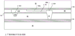
Referring to fig. 8C and 9, second wafer 86 is bonded to first wafer 80 (step 904), for example using thermal bonding or another wafer bonding technique, to form assembly 96. In particular, the second wafer 86 is bonded to the first wafer 80 such that the mask layer side of the first wafer 80 is in contact with the mask layer side of the second wafer 86. The opening 200 may be aligned with the opening through which the nozzle 22 is to be provided. Thus, the mask layer 81 may be bonded to the mask layer 87. In some embodiments, the mask layer 81 and/or the mask layer 87 are removed prior to bonding the second wafer 86 to the first wafer 80.
The etch stop layer 90 covers the recess 506. Thus, the etch stop layer 90 may provide the membrane 502 and define the cavity 500. Although only one recess 506 is shown in FIG. 8B, there may be multiple recesses to form multiple cavities. Additionally, although the cavity 500 is shown in fig. 8F-8G below the return channel 28, a similar cavity may additionally or alternatively be formed below the supply channel 24 by forming a recess in place.
Similarly, opening 200 is formed completely through mask layer 87 and device layer 88, for example using standard microfabrication techniques including photolithography and etching, to provide a portion of descender 20.
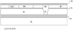
Referring to fig. 8D and 9, the handle layer 92 of the second wafer 86 is removed (step 906), such as by grinding and polishing, wet etching, plasma etching, or other removal process.
Referring to fig. 8E and 9, the holes 302 are etched through the etch stop layer 90 to form a membrane 300, for example for a filter structure 320, that is positioned adjacent to the nozzle 22 and reaches the nozzle in the flow path of the fluid (see fig. 3B) (step 908).
In the method of fig. 8A-8E, device layer 82, mask layers 81, 87 (if present), and device layer 88 together may form nozzle layer 11. The method of fig. 8A-8E provides a thick, robust nozzle layer 11 that is not thinned by the fabrication of the film 300.
The resulting assembly 96 employing the formed recess 500, membrane 300, or both, may be further processed (step 910) to form a fluid ejector 150 of a printhead, such as described below and in U.S. patent No.7566118, the contents of which are incorporated herein by reference in their entirety.
For example, referring to fig. 8F and 8G, top surface 74 of assembly 96 (e.g., the exposed surface of etch stop layer 90) may be bonded to flow path wafer 76 (960). For example, the top surface 74 of the first wafer 60 may be bonded to the flow path wafer 76 using a low temperature bond, such as with an epoxy (e.g., benzocyclobutene (BCB)) or using a low temperature plasma activated bond.
The flow path wafer 76 may be fabricated prior to bonding to have flow channels 475, such as supply channel 14, chamber inlet channel 16, pumping chamber 18, descender 20, outlet channel 26, and outlet supply channel 28. Other elements, such as actuators (not shown), may be formed before or after assembly 96 is bonded to flow path wafer 76.
Referring to fig. 8G, after bonding, the handle layer 85 and etch stop layer 84 may be removed, such as by grinding and polishing, wet etching, plasma etching, or other removal process, to expose the nozzle 22. In some embodiments, the etch stop layer 84 is not removed, but holes are formed through the etch stop layer 84 to complete the nozzle. After the actuators are formed or attached, the resulting substrate generally corresponds to the substrate 110 shown in fig. 3C.
As shown in fig. 8G, the same layer 90 can provide a film 502 for the compliant microstructure (if present) and the film 300. As also shown in fig. 8G, the outlet channel 26 is formed as a recess in the bottom of the flow path wafer 76, and the top surface 74 of the assembly 96 of the first and second wafers may provide the lower surface of the outlet channel 26. Additionally, the top surface of the membrane 300 may be coplanar with the lower surface of the outlet channel 26.
Fig. 11A-11G illustrate another example method of fabricating the body 10 and the nozzle layer 11 of the substrate 110. In this example, the substrate is fabricated with a fluid ejector 150, the fluid ejector 150 having a membrane 300 in the fluid flow path prior to the intersection between the outlet channel 26 and the descender 20. The membrane 300 may provide a filter 320.
In addition, the substrate can be fabricated with one or more cavities 500 formed in the nozzle layer 11 to provide a compliant microstructure. Fluid ejector 150 having only membrane 300 or only chamber 500 may be fabricated according to a similar method. For example, to fabricate a fluid ejector without the cavity 500, one may simply start as shown in FIG. 11A, but the substrate lacks the recess 506.
Referring to fig. 11A and 12, a first wafer 80 (e.g., a silicon wafer or SOI wafer) includes a mask layer 81 (e.g., an oxide or nitride mask layer), a device layer 81 (e.g., silicon nozzle layer 11), an etch stop layer 84 (e.g., an oxide or nitride etch stop layer), and a handle layer 85 (e.g., a silicon handle layer). The first wafer 80 may be referred to as a nozzle wafer. In some examples, the first wafer 80 does not include the etch stop layer 84. In some examples, such as when the first wafer 80 is an SOI wafer, the insulating layer of the SOI wafer serves as the etch stop layer 84.
To define the nozzle locations, the mask layer 81 is patterned and openings are formed through the device layer 82 that will provide the nozzles 22 of the fluid ejectors 150 (step 920), for example using standard microfabrication techniques including photolithography and etching. For example, a first resist layer may be deposited onto the unpatterned masking layer 81 and photolithographically patterned. The mask layer 81 may be etched to form openings through the mask layer 81. The device layer 82 may then be etched using the mask layer 81 as a mask, for example using a Deep Reactive Ion Etch (DRIE), potassium hydroxide (KOH) etch, or other type of etch to form the nozzle 22. The first resist layer may be stripped.
Optionally, a recess 506 is also formed (step 922), extending partially but not completely through the device layer 82, for example using standard microfabrication techniques. If recesses 506 are to be formed, a second resist layer may be deposited onto masking layer 81 and photolithographically patterned. The mask layer 81 and the device layer 82 may be etched according to the patterned resist to form the recess 506, for example, using wet etching or dry etching.
Referring to fig. 11B and 12, a second wafer 86 (e.g., a silicon wafer or SOI wafer) has a handle layer 92, an etch stop layer 90 (e.g., an oxide or nitride etch stop layer), and a device layer 88. In some examples, such as when the second wafer 86 is an SOI wafer, the insulating layer of the SOI wafer 86 serves as the etch stop layer 90.
An opening 200 is formed completely through mask layer 87 and device layer 88, for example using standard microfabrication techniques including photolithography and etching, to provide a portion of descender 20. To define the openings 200, the mask layer 87 is patterned and openings 200 are formed in the device layer 88 of the second wafer 86, for example using standard microfabrication techniques including photolithography and etching. For example, a resist layer may be deposited onto the unpatterned mask layer 87 and photolithographically patterned. The mask layer 87 may be etched to form openings through the mask layer 87. Device layer 88 may then be etched using mask layer 87 as a mask.
An opening 510 may be formed through mask layer 87 and device layer 88 completely through a similar or identical process to provide a portion of return channel 28 (step 924).
In addition, a recessed region 202 may be formed in the top surface of device layer 88 between opening 200 and opening 510 to provide outlet channel 26 (step 924). Recessed region 202 may extend partially, but not completely, through device layer 88, leaving portion 88a of device layer 88 below recessed region 202. Thus, the openings 200 and 510 may be deeper than the recessed region 202. Alternatively, recessed region 202 may extend completely through device layer 88.
Referring to fig. 11C and 12, second wafer 86 is bonded to first wafer 80 (step 926), for example using thermal bonding or another wafer bonding technique, to form assembly 96. In particular, the second wafer 86 is bonded to the first wafer 80 such that the mask layer side of the first wafer 80 is in contact with the mask layer side of the second wafer 86. The opening 200 may be aligned with the opening through which the nozzle 22 is to be provided. Thus, the mask layer 81 may be bonded to the mask layer 87. In some embodiments, the mask layer 81 and/or the mask layer 87 are removed prior to bonding the second wafer 86 to the first wafer 80.
The channels forming recessed regions 202 between the top of the second wafer 86 and the portions 88a of the device layer 88 provide the outlet channels 26.
The etch stop layer 90 covers the recess 506. Thus, the etch stop layer 90 may provide the membrane 502 and define the cavity 500. Although only one recess 506 is shown in FIG. 11B, there may be multiple recesses to form multiple cavities 500. In addition, although the cavity 500 is shown in fig. 11F-11G below the return channel 28, a similar cavity may additionally or alternatively be formed below the supply channel 24 by forming a recess in place.
Referring to fig. 11D and 12, the handle layer 92 of the second wafer 86 is removed (step 928), such as by grinding and polishing, wet etching, plasma etching, or other removal process, leaving the etch stop layer 90 and the device layer 88.
Referring to fig. 11E and 12, a hole 302 is etched through etch stop layer 90 (step 930). Thus, the portion of the etch stop layer 90 having the aperture 302 forms a filter feature that is positioned proximate to the nozzle 22 and in the flow path of the fluid to the nozzle. In addition, a hole is etched through the etch stop layer 90 over the opening 510. This exposes an opening 510 that will become the lower portion of the return channel 28.
The method of fig. 11A-11E allows some control over the relative thicknesses of the films 300 and 502. That is, films 300 and 502 need not have the same thickness and/or composition, and thus the thickness and/or composition of each film may be selected for different purposes.
The wafer assembly 96 with the nozzles 22, optional recesses 500 formed in the device layer 88, and the membrane 300 positioned proximate the nozzles may be further processed, for example as described in U.S. patent No.7566118, the contents of which are incorporated herein by reference in their entirety, to form the fluid ejectors 150 of the printhead 100.
For example, referring to fig. 11F and 12, in some examples, the top surface 74 of the component 96 (e.g., the exposed surface of the etch stop layer 90) may be bonded to the flow path wafer 76 (step 932). For example, the top surface 74 of the first wafer 60 may be bonded to the flow path wafer 76 using a low temperature bond, such as with an epoxy (e.g., benzocyclobutene (BCB)) or using a low temperature plasma activated bond.
Flow path wafer 76 may be fabricated prior to bonding to have a portion of flow channels 475, such as supply channel 14, chamber inlet channel 16, pumping chamber 18, a portion of descender 20 (the remainder being provided by opening 200), and a portion of outlet supply channel 28 (the remainder being provided by opening 510). Other elements such as actuators (not shown) may be formed before or after assembly 96 is bonded to flow path wafer 76.
Referring to fig. 11G and 12, the handle layer 85 may then be removed, such as by grinding and polishing, wet etching, plasma etching, or other removal process (step 934). If present, the etch stop layer 84 is either removed (as shown in FIG. 11F) or masked and etched, for example using standard microfabrication techniques including photolithography and etching, to expose the nozzles (step 936).
After the actuator is formed or attached, the resulting substrate generally corresponds to the substrate shown in fig. 3D, although the bottom surface of the membrane 300 is slightly higher (by the thickness of the portion 88 a) than the intersection between the descender 20 and the outlet passage 26. On the other hand, if the recess 202 extends completely through the device layer 88, the bottom surface of the membrane 300 will be coplanar with the top surface of the outlet channel 26.
In the embodiment shown in fig. 11A-11G, outlet channels 26 are provided by recesses 202 in device layer 88 rather than recesses in wafer 76. Alternatively, outlet channels 26 may be provided by recesses in the bottom surface of flow path wafer 76 instead of device layer 88. In this case (similar to fig. 8F-8G), the top surface of the etch stop layer 90 provides the bottom surface of the outlet channel 26.
Fig. 13A-13E illustrate a process similar to that of fig. 8A-8G for fabricating the body 10 and nozzle layer 11 of the substrate 110. However, in this example, the hole 302 may pass through some or all of the device layers 88. Fabrication may be generally performed as described above with respect to fig. 11A-11G, except as described below.
In particular, referring to fig. 13B, rather than forming the hole 200 completely through the device layer 88, a recessed region 204 is formed where the nozzle 22 is located. The recessed region 204 may be the same depth or deeper than the recessed region 202 that will provide the outlet channel 26. As shown in fig. 13C-D, this leaves a thin portion 88b of the device layer 88, which thin portion 88b will cover the nozzle 22 when the first wafer is bonded to the second wafer.
Referring to fig. 13E, after forming the opening in etch stop layer 90, etch stop layer 90 may be used as a mask and the opening through thin portion 88b of device layer 88 may be etched, for example by reactive ion etching, until recess 204 is exposed. The resulting opening through etch stop layer 90 and thin portion 88b of device layer 88 provides a hole 302 through the film. Fabrication can then proceed as shown in FIGS. 11F-11G. An advantage of this approach is that it allows the thickness of the membrane 300 to be selected.
After forming or attaching the actuators, the resulting substrate generally corresponds to the substrate shown in fig. 3D. If the recessed region 204 has the same depth as the recessed region 202, the bottom surface of the membrane 300 will be coplanar with the top surface of the outlet channel 26.
Fig. 14A-14G illustrate another example method of fabricating the body 10 and the nozzle layer 11 of the substrate 110. In this example, the substrate is fabricated with the fluid ejector 150 with the membrane 300 in the outlet channel 26. In particular, the membrane 300 may be in the outlet channel 26 at a location spaced from the descender 20 and the return channel 28. The film may provide a resistive structure 310.
The substrate may also include a compliant microstructure that includes one or more cavities 500 formed in the nozzle layer 11. The fluid ejector 150 having only the membrane 300 may be manufactured according to a similar method. For example, to fabricate a fluid ejector without the cavity 500, portions of the steps associated with the formation of the recess 506 shown in FIG. 14B may simply be omitted.
Referring to fig. 14A and 15, a first wafer 80, such as a silicon wafer or a silicon-on-insulator (SOI) wafer, provides a nozzle wafer. The first wafer 80 includes a mask layer 81 (e.g., an oxide or nitride mask layer, such as SiO)2Or Si3N4) A device layer 82 (e.g., a silicon device layer 82), an etch stop layer 84 (e.g., an oxide or nitride etch stop layer), and a handle layer 85 (e.g., a silicon handle layer). In some examples, the first wafer 80 does not include the etch stop layer 84. In some examples, such as when the first wafer 80 is an SOI wafer, the insulating layer of the SOI wafer 80 serves as the etch stop layer 84.
To define the nozzle locations, the mask layer 81 is patterned and openings of the nozzles 22 that will provide the fluid ejectors 150 are formed through the device layer 82 (step 940), for example using standard microfabrication techniques including photolithography and etching. For example, a first resist layer may be deposited onto the unpatterned masking layer 81 and photolithographically patterned. The mask layer 81 may be etched to form openings through the mask layer 81. The device layer 82 may then be etched using the mask layer 81 as a mask, for example using a Deep Reactive Ion Etch (DRIE), potassium hydroxide (KOH) etch, or other type of etch to form the nozzle 22. The resist may be stripped before or after etching device layer 82.
Referring to fig. 14B and 15, a second wafer 86 (e.g., a silicon wafer or SOI wafer) includes a mask layer 87 (e.g., an oxide or nitride mask layer), a device layer 88 (e.g., a silicon device layer 88), an etch stop layer 90 (e.g., an oxide or nitride etch stop layer 90), and a handle layer 92 (e.g., a silicon handle layer 92). Device layer 88 of second wafer 86 may be formed of the same material as device layer 82 of first wafer 80. In some examples, such as when the second wafer 86 is an SOI wafer, the insulating layer of the SOI wafer 86 serves as the etch stop layer 90.
To define the cavity 500, the mask layer 87 is patterned and recesses 506 are formed in the device layer 88 of the second wafer 86 (step 942), for example using standard microfabrication techniques including photolithography and etching. Although fig. 14B shows the recess 510 extending completely through the device layer 88, this is not required; the recess 500 may extend only partially through the device layer 88.
An opening is formed in mask layer 87 and, optionally, recess 200 is formed at least partially through device layer 88, for example using standard microfabrication techniques including photolithography and etching. This recess 200 will be located below the outlet passage 26 and may be considered part of the provision of the descender 20 or nozzle 22. Fig. 14B shows the recess 200 as an opening extending completely through the device layer 88, but this is not required; the recess 200 may extend only partially through the device layer 88.
Similarly, an opening is formed in mask layer 87, and recess 208 is formed at least partially through device layer 88 (step 944). This recess will provide a part of the outlet channel 26. Fig. 14B shows that recess 208 extends completely through device layer 88, but is not required; the recess 208 may extend only partially through the device layer 88. However, the recess 200 should be at least as deep as the recess 208.
The recess 506 (if present), the opening 200, and the recess 208 may be formed simultaneously in a single etching step. In this case, the recess 510 (if present), the opening 200 and the recess 208 will all have the same depth. For example, a resist layer may be deposited on the unpatterned mask layer 87 and photolithographically patterned. The mask layer 87 may be etched to form openings through the mask layer 87. Device layer 88 may then be etched using mask layer 87 as a mask.
On the other hand, to provide the recesses 510 (if present), the openings 200 and the recesses 208 with different depths, multiple etching steps may be used. For example, for each feature, a layer of resist may be deposited and photolithographically patterned, and then the substrate subjected to an etching step (the resist may cover the previously defined features to protect them from subsequent etching steps). In some embodiments, the photoresist itself may be used as a mask.
Referring to fig. 14C and 15, second wafer 86 is bonded to first wafer 80 (step 946), for example using thermal bonding or another wafer bonding technique, to form assembly 96. In particular, the second wafer 86 is bonded to the first wafer 80 such that the mask layer side of the first wafer 80 is in contact with the mask layer side of the second wafer 86. Thus, the mask layer 81 may be bonded to the mask layer 87. In some embodiments, masking layer 81 and masking layer 87 are removed before second wafer 86 is bonded to first wafer 80. The opening 200 may be aligned with the opening through which the nozzle 22 is to be provided. When the recess 510 is covered by the etch stop layer 90, it forms a cavity 500.
The etch stop layer 90 covers the recess 506. Thus, the etch stop layer 90 may provide the membrane 502 and define the cavity 500. Although only one recess 506 is shown in FIG. 14B, there may be multiple recesses to form multiple cavities 500. In addition, while the cavity 500 shown in fig. 14F-14G is below the return channel 28, a similar cavity may additionally or alternatively be formed below the supply channel 24 by forming a recess in place.
Referring to fig. 14D and 15, the handle layer 92 of the second wafer 86 is removed (step 948), such as by grinding and polishing, wet etching, plasma etching, or other removal process.
Referring to fig. 14E and 15, the hole 302 is etched through the etch stop layer 90 until the recess 208 is reached (step 950) to form the impedance feature 300. The holes 302 may be formed by an etching process such as wet etching or plasma etching. In particular, the holes 302 may be formed by anisotropic etching, such as reactive ion etching.
Additionally, an aperture 340 may be formed through the etch stop layer 90 until the recess 208 is reached to provide an opening between the outlet channel 26 and the return channel 28 (step 950).
In addition, a hole 342 may be formed through etch stop layer 90 until reaching recess 200 to provide an opening between descender 20 and nozzle 22.
Referring to fig. 16A-16C, if the recess 208 does not extend completely through the device layer 88, a further etching step may be performed, for example using the etch stop layer 90 as a mask. Openings 302 and 340 through thin portion 88c of device layer 88 may be etched over recess 208, for example by reactive ion etching, until recess 208 is exposed. An advantage of this approach is that it allows the thickness of the membrane 300 to be selected, for example by selecting the depth of the recess 208. The aspects shown in fig. 16A-16C may be combined with various alternatives.
Assuming that recess 208 extends completely through device layer 88, as shown in fig. 14E, the portion of etch stop layer 90 that spans flow path 26 provides membrane 300. On the other hand, if the recess 208 extends only partially through the device layer 88 shown in fig. 16B, the combination of the etch stop layer 90 and the thin portion 88c of the device layer 88 provides the film 300.
In the method illustrated in fig. 14A-14E, the device layer 82, the mask layers 81, 87 (if present), the device layer 88, and the etch stop layer 90 may provide the nozzle layer 11. The method of fig. 14A-14E provides a thick, robust nozzle layer 11 that is not thinned by the fabrication of the membrane 304. The resulting assembly 96 with the cavity 500 and/or membrane 300 may be further processed to form a fluid ejector 150 of a printhead.
For example, referring to fig. 14F and 14G, the top surface 74 of the assembly 96 (e.g., the exposed surface of the etch stop layer 90) may be bonded to the flow path wafer 76 (step 952). The flow path wafer 76 may be fabricated prior to bonding to have flow channels 475, such as supply channel 14, chamber inlet channel 16, pumping chamber 18, descender 20, a portion of outlet channel 26, and outlet supply channel 28. For example, the top surface 74 of the first wafer 60 may be bonded to the flow path wafer 76 using a low temperature bond, such as with an epoxy (e.g., benzocyclobutene (BCB)) or using a low temperature plasma activated bond. Other elements such as actuators (not shown) may be formed before or after assembly 96 is bonded to flow path wafer 76.
In the embodiment shown in fig. 14A-14G, a portion of the outlet channel 26 is provided by the recess 208 in the device layer 88 and another portion of the outlet channel 26 is provided by the recess 27 in the bottom of the flow path wafer 76. A recess 27 in the bottom may extend from the descender 20. The recess 208 and the recess 27 overlap the aperture 302 such that the resulting membrane 300 divides the outlet channel 26 into a first region 26a above the membrane 304 and a second region 26b below the membrane.
Although the embodiment shown in fig. 14A-14G has an upper portion 26a connected to the outlet passage 26 of the descender 20 and a lower portion 26b connected to the outlet passage of the return passage 28, this may be reversed as shown in fig. 17A. For example, the recess 27 in the bottom of the flow path wafer 76 may extend from the return channel 28 to the opening 302 instead of the descender 20. Further, the recess 208 may be connected to (and considered to be a part of) the opening 200. Thus, the recess 208 may extend from the descender 20 to the opening 302.
Also, the embodiment shown in fig. 17A may be combined with various other aspects. For example, as shown in fig. 17B, the recess 208 may be formed such that it extends only partially through the device layer 88, and a further etching step may be performed, for example using the etch stop layer 90 as a mask. Accordingly, an opening 302 is etched through thin portion 88d of device layer 88 over recess 208, such as by reactive ion etching, until recess 208 is exposed. As a result, the combination of the etch stop layer 90 and the thin portion 88c of the device layer 88 provides the film 300 of the impedance feature 310.
Referring to fig. 14G and 15, after bonding, the handle layer 85 and etch stop layer 84 may be removed (step 954), such as by grinding and polishing, wet etching, plasma etching, or other removal process, to expose the nozzle 22. In some embodiments, the etch stop layer 84 is not removed, but an aperture is formed through the etch stop layer 84 to complete the nozzle (step 956). After forming or attaching the actuators, the resulting substrate generally corresponds to the substrate shown in fig. 3C.
As shown in fig. 14G, the same layer 90 can provide a film 502 for the compliant microstructure (if present) and the film 300. As also shown in fig. 14G, the outlet channel 26 is formed as a recess in the bottom of the flow path wafer 76, and the top surface 74 of the assembly 96 of the first and second wafers may provide the lower surface of the outlet channel 26. Additionally, the top surface of the membrane 300 may be coplanar with the lower surface of the outlet channel 26. Similarly, the top surface of the membrane 300 may be coplanar with the lower surface of the return channel 28.
Fig. 18A-18H illustrate a process similar to that of fig. 14-14G in which the body 10 and the nozzle layer 11 of the substrate 110 are fabricated. However, in this example, the opening 302 is located directly below the return passage 28 rather than within the outlet passage 26. Fabrication may be generally performed as described above for fig. 14A-14G and 17A, except as described below.
Referring to fig. 18B, a first recess 200 is formed in the device layer 88 in a region corresponding to the nozzle 22. This recess 200 will be below the outlet passage 26 and may be considered to provide part of the descender 20 or nozzle 22. A second recess 220 is formed in the device layer 88 in a region that will underlie a portion of the return channel 28. These recesses 200 and 220 may be formed by patterning the mask layer 87 and using it as a mask for etching the device layer 88.
In addition, referring to fig. 18C, a third recess 222 in the device layer 88 connects the first recess 200 and the second recess 220. A portion 88e of device layer 88 may remain under recess 222. The recess 222 may be formed by patterning the mask layer 87 and using it as a mask for etching the device layer 88. Alternatively, the mask layer 87 may be peeled off from the entire wafer 86.
Although fig. 18B-18C illustrate recess 200 and recess 220 as openings that extend completely through device layer 88, this is not required. Recesses 200 and/or recesses 220 may extend only partially through device layer 88. However, the recess 220 should be at least as deep (i.e., the same or greater depth) as the recess 222. Similarly, although fig. 18B shows recess 222 extending only partially through device layer 88, this is not required. The recess 222 may extend completely through the device layer 88. Where the recesses 200, 220, 222 have the same depth, they may be formed simultaneously in a single etching step. The relative depth of the recess may be selected as required by the height of the outlet channel 26 and the thickness of the membrane 300, for example based on the required fluid flow resistance.
Fig. 18D is performed similarly to fig. 14C, with the first wafer 80 bonded to the second wafer 86 to form the assembly 98 and the opening 200 aligned with the nozzle 22. Fig. 18E proceeds similarly to fig. 14D, with the handle layer 92 removed.
Referring to fig. 18F, a hole 302 is etched through the etch stop layer 90 until the recess 220 is reached to form the impedance feature 300. The holes 302 may be formed by an etching process, such as wet etching or plasma etching. In particular, the holes 302 may be formed by anisotropic etching, such as reactive ion etching.
In addition, a hole 342 may be formed through etch stop layer 90 until reaching recess 200 to provide an opening between descender 20 and nozzle 22.
If the recess 220 does not extend completely through the device layer 88, a further etching step may be performed, for example using the etch stop layer 90 as a mask. Similarly, if the recess 200 does not extend completely through the device layer 88, a further etching step may be performed, for example using the etch stop layer 90 as a mask. Accordingly, openings 302 and 342 may be etched through thin portion 88e of device layer 88, for example by reactive ion etching, until recess 208 is exposed.
Assuming that the recess 220 extends completely through the device layer 88, as shown in fig. 18F, the portion of the etch stop layer 90 between the outlet channel 26 and the return channel 28 provides a membrane 300. On the other hand, if the recess 220 extends only partially through the device layer 88 (e.g., in an equivalent manner as shown in fig. 16C), the combination of the etch stop layer 90 and the thin portion 88e of the device layer 88 provides the membrane 300.
Referring to fig. 18G, a top surface 74 of the component 96, such as an exposed surface of the etch stop layer 90, may be bonded to the flow path wafer 76. Fig. 18G proceeds similarly to fig. 14F, but the flow path wafer 76 does not have any recesses defining the outlet channels 26, as it is fully defined in the device layer 88.
Fig. 18H proceeds similarly to fig. 14G, where the handle layer 85 and the etch stop layer 84 are removed or the handle layer 85 is removed and a hole is formed through the etch stop layer 84 to complete the nozzle. After forming or attaching the actuators, the resulting substrate generally corresponds to the substrate shown in fig. 3B.
Referring to fig. 10, in some embodiments, a mask 40 including a plurality of openings 42 (e.g., rectangular openings) may be used to define apertures 302 of a desired size for the film 300. Each opening 42 corresponds to a unit area 44 defined by the corners of the opening 42, and the openings 42 are sized and oriented so that adjacent unit areas 44 overlap. The area of each unit region 44 is approximately the square of the length of the long side l of the corresponding opening 42. Using an anisotropic etch process (e.g., a potassium hydroxide etch process), a hole of the correct size can be made by continuing the anisotropic etch until the termination crystal plane (e.g., <111> plane) is reached. For example, the corners of each opening 42 may be positioned to expose the <111> plane such that each opening 42 will have the area defined by its corresponding cell region 44 etched. Since adjacent cell regions 44 overlap, the entire region can be opened by this etching process.
In some examples, a thick layer 82 (e.g., 30 μm, 50 μm, or 100 μm thick) may be used. The use of a thick nozzle wafer minimizes the risk of the nozzle fabrication process thinning the nozzle wafer to the point where the nozzle wafer is weakened.
The particular flow path configuration of the passage 14, the inlet passage 16, and the pumping chamber 18 that is common to the various embodiments is only one example of a flow path configuration. The methods of filter characterization or impedance characterization described below may be used for many other flow path configurations. For example, if the supply channel 14 is located at the same height as the pumping chamber 18, the riser 16a is not necessary. As another example, an additional horizontal passage may be positioned between pumping chamber 18 and nozzle 22. In general, the discussion of the descender may be generalized to a first passage connecting the pumping chamber to the inlet of the nozzle, and the discussion of the outlet passage may be generalized to a second passage connecting the inlet of the nozzle to the return passage.
The designation of various elements as first or second, e.g., first and second wafers, does not necessarily indicate an order in which the elements are manufactured. Although positioning terms such as "above" and "below" are used, these terms are used to indicate relative positioning of elements within the system, and do not necessarily denote position relative to gravity.
Specific embodiments have been described. Other embodiments are within the scope of the following claims.
Claims (18)
1. A fluid ejector comprising:
a nozzle layer having an outer surface and an inner surface and a nozzle extending between the inner and outer surfaces, the nozzle having an inlet at the inner surface to receive a fluid and an outlet at the outer surface for ejecting the fluid;
a body to which an inner surface of the nozzle layer is secured, the body comprising a pumping chamber, a return channel, and a first channel fluidly connecting the pumping chamber to an inlet of a nozzle;
a second channel fluidly connecting an inlet of the nozzle to the return channel;
an actuator configured to cause fluid to flow out of the pumping chamber such that actuation of the actuator causes fluid to be ejected from a nozzle;
a first membrane disposed between the actuator and the pumping chamber; and
a second membrane, distinct from the first membrane, positioned to span and partially block an inlet of the nozzle, the second membrane having at least one aperture therethrough such that, in operation of the fluid ejector, fluid flows through the at least one aperture in the second membrane.
2. The fluid ejector of claim 1, wherein the second membrane and orifice are configured such that the first channel has a first impedance when fluid is ejected from the nozzle and a second impedance when fluid is not ejected from the nozzle.
3. The fluid ejector of claim 2, wherein the first impedance is greater than the second impedance.
4. The fluid ejector of claim 2, wherein the second membrane is configured such that the second channel has a maximum impedance at or near a resonant frequency of the nozzle.
5. The fluid ejector of claim 1, wherein the second membrane extends substantially parallel to the outer surface.
6. The fluid ejector of claim 1, wherein the second membrane has a plurality of holes therethrough.
7. The fluid ejector of claim 6, wherein the plurality of holes are evenly spaced on the second membrane.
8. The fluid ejector of claim 1, wherein the first membrane extends parallel to the outer surface and across the fluid ejector, and wherein the first membrane comprises a portion of a film layer.
9. The fluid ejector of claim 8, wherein the film layer is located between the body and the nozzle layer.
10. The fluid ejector of claim 1, wherein the orifice is spaced from a wall of the nozzle on all sides of the orifice.
11. The fluid ejector of claim 1, wherein the second membrane projects inwardly substantially perpendicular to a wall of the nozzle.
12. The fluid ejector of claim 1, wherein the second membrane is formed of a material having a lower modulus of elasticity than a material forming a wall of the nozzle.
13. The fluid ejector of claim 1, wherein the second membrane is more flexible than a wall of the nozzle.
14. The fluid ejector of claim 1, wherein the aperture through the second membrane is narrower than the outlet opening of the nozzle.
15. The fluid ejector of claim 1, wherein the second film is formed of an oxide.
16. The fluid ejector of claim 15, wherein the second membrane has a thickness between 0.5 μ ι η and 5 μ ι η.
17. The fluid ejector of claim 1, wherein the second membrane is formed from a polymer.
18. The fluid ejector of claim 17, wherein the second membrane has a thickness between 10 μ ι η and 30 μ ι η.
Priority Applications (1)
| Application Number | Priority Date | Filing Date | Title |
|---|---|---|---|
| CN202110060536.2A CN112895718B (en) | 2015-12-31 | 2016-12-30 | Fluid ejection device |
Applications Claiming Priority (3)
| Application Number | Priority Date | Filing Date | Title |
|---|---|---|---|
| US201562273891P | 2015-12-31 | 2015-12-31 | |
| US62/273,891 | 2015-12-31 | ||
| PCT/US2016/069462 WO2017117518A1 (en) | 2015-12-31 | 2016-12-30 | Fluid ejection devices |
Related Child Applications (1)
| Application Number | Title | Priority Date | Filing Date |
|---|---|---|---|
| CN202110060536.2A Division CN112895718B (en) | 2015-12-31 | 2016-12-30 | Fluid ejection device |
Publications (2)
| Publication Number | Publication Date |
|---|---|
| CN108698405A CN108698405A (en) | 2018-10-23 |
| CN108698405B true CN108698405B (en) | 2021-02-02 |
Family
ID=59225466
Family Applications (2)
| Application Number | Title | Priority Date | Filing Date |
|---|---|---|---|
| CN201680082235.7A Active CN108698405B (en) | 2015-12-31 | 2016-12-30 | Fluid ejection device |
| CN202110060536.2A Active CN112895718B (en) | 2015-12-31 | 2016-12-30 | Fluid ejection device |
Family Applications After (1)
| Application Number | Title | Priority Date | Filing Date |
|---|---|---|---|
| CN202110060536.2A Active CN112895718B (en) | 2015-12-31 | 2016-12-30 | Fluid ejection device |
Country Status (5)
| Country | Link |
|---|---|
| US (3) | US10315421B2 (en) |
| EP (1) | EP3397493A4 (en) |
| JP (3) | JP6883042B2 (en) |
| CN (2) | CN108698405B (en) |
| WO (1) | WO2017117518A1 (en) |
Families Citing this family (16)
| Publication number | Priority date | Publication date | Assignee | Title |
|---|---|---|---|---|
| US10315421B2 (en) | 2015-12-31 | 2019-06-11 | Fujifilm Dimatix, Inc. | Fluid ejection devices |
| EP3330329B1 (en) * | 2016-12-02 | 2022-06-08 | Ricoh Company, Ltd. | Inkjet recording apparatus, printer, and method for manufacturing cured product |
| EP3634763B1 (en) * | 2017-06-09 | 2023-12-13 | Fujifilm Dimatix, Inc. | Fluid ejection apparatus with reduced crosstalk, corresponding operating method and making method |
| JP7031376B2 (en) * | 2018-03-04 | 2022-03-08 | 株式会社リコー | Liquid discharge head, liquid discharge unit, liquid discharge device |
| JP7106917B2 (en) * | 2018-03-23 | 2022-07-27 | セイコーエプソン株式会社 | Liquid ejecting head and liquid ejecting device |
| WO2019244227A1 (en) * | 2018-06-19 | 2019-12-26 | コニカミノルタ株式会社 | Ink jet head and ink jet recording device |
| JP2020100136A (en) * | 2018-12-21 | 2020-07-02 | セイコーエプソン株式会社 | Liquid jet head, liquid jet device and liquid jet system |
| JP7287042B2 (en) * | 2018-12-21 | 2023-06-06 | セイコーエプソン株式会社 | Liquid jet head and liquid jet system |
| US11007789B2 (en) | 2018-12-21 | 2021-05-18 | Seiko Epson Corporation | Liquid ejecting head and liquid ejecting apparatus |
| US11104128B2 (en) * | 2018-12-21 | 2021-08-31 | Seiko Epson Corporation | Liquid ejecting head and liquid ejecting system |
| JP7293670B2 (en) * | 2019-01-29 | 2023-06-20 | ブラザー工業株式会社 | liquid ejection head |
| IT201900005808A1 (en) * | 2019-04-15 | 2020-10-15 | St Microelectronics Srl | MICROPUMP MEMS DEVICE FOR HANDLING OR EJECTION OF A FLUID, IN PARTICULAR MICROSOFT OR FLOWMETER |
| IT201900007196A1 (en) * | 2019-05-24 | 2020-11-24 | St Microelectronics Srl | MICROFLUID DEVICE FOR CONTINUOUS EXPULSION OF FLUIDS, IN PARTICULAR FOR INK PRINTING, AND RELATED MANUFACTURING PROCEDURE |
| JP7302385B2 (en) | 2019-08-29 | 2023-07-04 | セイコーエプソン株式会社 | Liquid ejection head unit and liquid ejection device |
| KR20210077049A (en) * | 2019-12-16 | 2021-06-25 | 현대자동차주식회사 | Ejector nozzle and ejector including the same |
| JP7413864B2 (en) * | 2020-03-19 | 2024-01-16 | セイコーエプソン株式会社 | Method for manufacturing liquid jet head and method for manufacturing channel parts |
Family Cites Families (25)
| Publication number | Priority date | Publication date | Assignee | Title |
|---|---|---|---|---|
| US3958255A (en) * | 1974-12-31 | 1976-05-18 | International Business Machines Corporation | Ink jet nozzle structure |
| JPH0365352A (en) | 1989-08-03 | 1991-03-20 | Canon Inc | Ink-jet recording device and ink supplying device therefor |
| ATE139941T1 (en) | 1990-02-26 | 1996-07-15 | Canon Kk | INK JET RECORDING APPARATUS AND METHOD FOR CLEANING THE RECORDING HEAD |
| US5828394A (en) * | 1995-09-20 | 1998-10-27 | The Board Of Trustees Of The Leland Stanford Junior University | Fluid drop ejector and method |
| JP3372765B2 (en) | 1996-07-12 | 2003-02-04 | キヤノン株式会社 | Liquid ejection head, head cartridge, liquid ejection device, recording system, head kit, and method of manufacturing liquid ejection head |
| US7052117B2 (en) * | 2002-07-03 | 2006-05-30 | Dimatix, Inc. | Printhead having a thin pre-fired piezoelectric layer |
| CN100548692C (en) * | 2003-10-10 | 2009-10-14 | 富士胶卷迪马蒂克斯股份有限公司 | Printhead with film |
| US7347532B2 (en) * | 2004-08-05 | 2008-03-25 | Fujifilm Dimatix, Inc. | Print head nozzle formation |
| JP5003282B2 (en) * | 2007-05-23 | 2012-08-15 | 富士ゼロックス株式会社 | Droplet discharge head and image forming apparatus |
| BRPI0912897A2 (en) * | 2008-05-23 | 2015-10-06 | Fujifilm Corp | fluid droplet ejection |
| US8761720B2 (en) * | 2008-07-03 | 2014-06-24 | Centurylink Intellectual Property Llc | System and method for generating and communicating updated emergency messages |
| JP5298790B2 (en) * | 2008-11-12 | 2013-09-25 | セイコーエプソン株式会社 | Fluid ejecting apparatus and fluid ejecting method |
| US8303082B2 (en) * | 2009-02-27 | 2012-11-06 | Fujifilm Corporation | Nozzle shape for fluid droplet ejection |
| US8210649B2 (en) | 2009-11-06 | 2012-07-03 | Fujifilm Corporation | Thermal oxide coating on a fluid ejector |
| US8317302B2 (en) * | 2010-03-18 | 2012-11-27 | Fujifilm Corporation | Restriction of fluid ejector membrane |
| US8272717B2 (en) * | 2010-03-29 | 2012-09-25 | Fujifilm Corporation | Jetting device with reduced crosstalk |
| US8267504B2 (en) * | 2010-04-27 | 2012-09-18 | Eastman Kodak Company | Printhead including integrated stimulator/filter device |
| US20120098899A1 (en) | 2010-10-26 | 2012-04-26 | Yonglin Xie | Dispensing liquid using dispenser with return filter |
| JP2013116590A (en) * | 2011-12-02 | 2013-06-13 | Ricoh Co Ltd | Liquid droplet ejection head and image forming apparatus |
| EP2620286A1 (en) * | 2012-01-26 | 2013-07-31 | Nederlandse Organisatie voor toegepast -natuurwetenschappelijk onderzoek TNO | Continuous jet printing of a fluid material |
| CN104302483B (en) * | 2012-07-03 | 2016-09-21 | 惠普发展公司,有限责任合伙企业 | Fluid ejection device |
| JP2014061695A (en) * | 2012-09-20 | 2014-04-10 | Samsung Electro-Mechanics Co Ltd | Inkjet print head |
| KR20140076136A (en) * | 2012-12-12 | 2014-06-20 | 삼성전기주식회사 | Inkjet print head |
| US9162454B2 (en) * | 2013-04-11 | 2015-10-20 | Eastman Kodak Company | Printhead including acoustic dampening structure |
| US10315421B2 (en) | 2015-12-31 | 2019-06-11 | Fujifilm Dimatix, Inc. | Fluid ejection devices |
-
2016
- 2016-12-30 US US15/395,549 patent/US10315421B2/en active Active
- 2016-12-30 WO PCT/US2016/069462 patent/WO2017117518A1/en active Application Filing
- 2016-12-30 JP JP2018533915A patent/JP6883042B2/en active Active
- 2016-12-30 CN CN201680082235.7A patent/CN108698405B/en active Active
- 2016-12-30 CN CN202110060536.2A patent/CN112895718B/en active Active
- 2016-12-30 EP EP16882747.5A patent/EP3397493A4/en active Pending
-
2019
- 2019-04-25 US US16/394,073 patent/US11001059B2/en active Active
-
2021
- 2021-04-28 US US17/242,621 patent/US11904610B2/en active Active
- 2021-05-07 JP JP2021079130A patent/JP7277508B2/en active Active
-
2023
- 2023-05-08 JP JP2023076590A patent/JP2023093768A/en active Pending
Also Published As
| Publication number | Publication date |
|---|---|
| JP2019505411A (en) | 2019-02-28 |
| US10315421B2 (en) | 2019-06-11 |
| US11904610B2 (en) | 2024-02-20 |
| EP3397493A1 (en) | 2018-11-07 |
| JP6883042B2 (en) | 2021-06-02 |
| US20210245508A1 (en) | 2021-08-12 |
| US20190248138A1 (en) | 2019-08-15 |
| US20170190179A1 (en) | 2017-07-06 |
| JP7277508B2 (en) | 2023-05-19 |
| CN112895718A (en) | 2021-06-04 |
| JP2021175609A (en) | 2021-11-04 |
| EP3397493A4 (en) | 2019-08-14 |
| JP2023093768A (en) | 2023-07-04 |
| WO2017117518A1 (en) | 2017-07-06 |
| CN112895718B (en) | 2022-09-13 |
| CN108698405A (en) | 2018-10-23 |
| US11001059B2 (en) | 2021-05-11 |
Similar Documents
| Publication | Publication Date | Title |
|---|---|---|
| CN108698405B (en) | Fluid ejection device | |
| JP7314206B2 (en) | Fluid ejection device with reduced crosstalk | |
| EP1693206B1 (en) | Piezoelectric inkjet printhead and method of manufacturing the same | |
| KR100438836B1 (en) | Piezo-electric type inkjet printhead and manufacturing method threrof | |
| EP3173235B1 (en) | Fluid ejection device with restriction channel, and manufacturing method thereof | |
| KR100682917B1 (en) | Piezo-electric type inkjet printhead and method of manufacturing the same | |
| KR20070040395A (en) | Print head nozzle formation | |
| KR100590558B1 (en) | Piezo-electric type ink jet printhead and manufacturing method thereof | |
| EP2332169B1 (en) | Bonding on silicon substrate having a groove | |
| US20110250403A1 (en) | Bonding on silicon substrate | |
| KR100528349B1 (en) | Piezo-electric type inkjet printhead and manufacturing method threrof | |
| KR100908115B1 (en) | Inkjet printhead with ink supply structure through porous medium and its manufacturing method | |
| JP6317650B2 (en) | Working fluid layer of thermopneumatic actuator | |
| KR100561865B1 (en) | Piezo-electric type inkjet printhead and manufacturing method threrof | |
| US9004652B2 (en) | Thermo-pneumatic actuator fabricated using silicon-on-insulator (SOI) |
Legal Events
| Date | Code | Title | Description |
|---|---|---|---|
| PB01 | Publication | ||
| PB01 | Publication | ||
| SE01 | Entry into force of request for substantive examination | ||
| SE01 | Entry into force of request for substantive examination | ||
| GR01 | Patent grant | ||
| GR01 | Patent grant |