CN1086346C - Card mounted with circuit chip and circuit chip module - Google Patents
Card mounted with circuit chip and circuit chip module Download PDFInfo
- Publication number
- CN1086346C CN1086346C CN97181047A CN97181047A CN1086346C CN 1086346 C CN1086346 C CN 1086346C CN 97181047 A CN97181047 A CN 97181047A CN 97181047 A CN97181047 A CN 97181047A CN 1086346 C CN1086346 C CN 1086346C
- Authority
- CN
- China
- Prior art keywords
- circuit chip
- card
- intensive aspect
- chip
- buffer component
- Prior art date
- Legal status (The legal status is an assumption and is not a legal conclusion. Google has not performed a legal analysis and makes no representation as to the accuracy of the status listed.)
- Expired - Fee Related
Links
Images


Classifications
-
- G—PHYSICS
- G06—COMPUTING; CALCULATING OR COUNTING
- G06K—GRAPHICAL DATA READING; PRESENTATION OF DATA; RECORD CARRIERS; HANDLING RECORD CARRIERS
- G06K19/00—Record carriers for use with machines and with at least a part designed to carry digital markings
- G06K19/06—Record carriers for use with machines and with at least a part designed to carry digital markings characterised by the kind of the digital marking, e.g. shape, nature, code
- G06K19/067—Record carriers with conductive marks, printed circuits or semiconductor circuit elements, e.g. credit or identity cards also with resonating or responding marks without active components
- G06K19/07—Record carriers with conductive marks, printed circuits or semiconductor circuit elements, e.g. credit or identity cards also with resonating or responding marks without active components with integrated circuit chips
- G06K19/077—Constructional details, e.g. mounting of circuits in the carrier
- G06K19/07745—Mounting details of integrated circuit chips
- G06K19/07747—Mounting details of integrated circuit chips at least one of the integrated circuit chips being mounted as a module
-
- G—PHYSICS
- G06—COMPUTING; CALCULATING OR COUNTING
- G06K—GRAPHICAL DATA READING; PRESENTATION OF DATA; RECORD CARRIERS; HANDLING RECORD CARRIERS
- G06K19/00—Record carriers for use with machines and with at least a part designed to carry digital markings
- G06K19/06—Record carriers for use with machines and with at least a part designed to carry digital markings characterised by the kind of the digital marking, e.g. shape, nature, code
- G06K19/067—Record carriers with conductive marks, printed circuits or semiconductor circuit elements, e.g. credit or identity cards also with resonating or responding marks without active components
- G06K19/07—Record carriers with conductive marks, printed circuits or semiconductor circuit elements, e.g. credit or identity cards also with resonating or responding marks without active components with integrated circuit chips
- G06K19/077—Constructional details, e.g. mounting of circuits in the carrier
- G06K19/0772—Physical layout of the record carrier
- G06K19/07728—Physical layout of the record carrier the record carrier comprising means for protection against impact or bending, e.g. protective shells or stress-absorbing layers around the integrated circuit
-
- G—PHYSICS
- G06—COMPUTING; CALCULATING OR COUNTING
- G06K—GRAPHICAL DATA READING; PRESENTATION OF DATA; RECORD CARRIERS; HANDLING RECORD CARRIERS
- G06K19/00—Record carriers for use with machines and with at least a part designed to carry digital markings
- G06K19/06—Record carriers for use with machines and with at least a part designed to carry digital markings characterised by the kind of the digital marking, e.g. shape, nature, code
- G06K19/067—Record carriers with conductive marks, printed circuits or semiconductor circuit elements, e.g. credit or identity cards also with resonating or responding marks without active components
- G06K19/07—Record carriers with conductive marks, printed circuits or semiconductor circuit elements, e.g. credit or identity cards also with resonating or responding marks without active components with integrated circuit chips
- G06K19/077—Constructional details, e.g. mounting of circuits in the carrier
- G06K19/07745—Mounting details of integrated circuit chips
-
- G—PHYSICS
- G06—COMPUTING; CALCULATING OR COUNTING
- G06K—GRAPHICAL DATA READING; PRESENTATION OF DATA; RECORD CARRIERS; HANDLING RECORD CARRIERS
- G06K19/00—Record carriers for use with machines and with at least a part designed to carry digital markings
- G06K19/06—Record carriers for use with machines and with at least a part designed to carry digital markings characterised by the kind of the digital marking, e.g. shape, nature, code
- G06K19/067—Record carriers with conductive marks, printed circuits or semiconductor circuit elements, e.g. credit or identity cards also with resonating or responding marks without active components
- G06K19/07—Record carriers with conductive marks, printed circuits or semiconductor circuit elements, e.g. credit or identity cards also with resonating or responding marks without active components with integrated circuit chips
- G06K19/077—Constructional details, e.g. mounting of circuits in the carrier
- G06K19/07749—Constructional details, e.g. mounting of circuits in the carrier the record carrier being capable of non-contact communication, e.g. constructional details of the antenna of a non-contact smart card
- G06K19/0775—Constructional details, e.g. mounting of circuits in the carrier the record carrier being capable of non-contact communication, e.g. constructional details of the antenna of a non-contact smart card arrangements for connecting the integrated circuit to the antenna
-
- G—PHYSICS
- G06—COMPUTING; CALCULATING OR COUNTING
- G06K—GRAPHICAL DATA READING; PRESENTATION OF DATA; RECORD CARRIERS; HANDLING RECORD CARRIERS
- G06K19/00—Record carriers for use with machines and with at least a part designed to carry digital markings
- G06K19/06—Record carriers for use with machines and with at least a part designed to carry digital markings characterised by the kind of the digital marking, e.g. shape, nature, code
- G06K19/067—Record carriers with conductive marks, printed circuits or semiconductor circuit elements, e.g. credit or identity cards also with resonating or responding marks without active components
- G06K19/07—Record carriers with conductive marks, printed circuits or semiconductor circuit elements, e.g. credit or identity cards also with resonating or responding marks without active components with integrated circuit chips
- G06K19/077—Constructional details, e.g. mounting of circuits in the carrier
- G06K19/07749—Constructional details, e.g. mounting of circuits in the carrier the record carrier being capable of non-contact communication, e.g. constructional details of the antenna of a non-contact smart card
- G06K19/07773—Antenna details
- G06K19/07777—Antenna details the antenna being of the inductive type
- G06K19/07779—Antenna details the antenna being of the inductive type the inductive antenna being a coil
- G06K19/07783—Antenna details the antenna being of the inductive type the inductive antenna being a coil the coil being planar
-
- H—ELECTRICITY
- H01—ELECTRIC ELEMENTS
- H01L—SEMICONDUCTOR DEVICES NOT COVERED BY CLASS H10
- H01L2224/00—Indexing scheme for arrangements for connecting or disconnecting semiconductor or solid-state bodies and methods related thereto as covered by H01L24/00
- H01L2224/01—Means for bonding being attached to, or being formed on, the surface to be connected, e.g. chip-to-package, die-attach, "first-level" interconnects; Manufacturing methods related thereto
- H01L2224/42—Wire connectors; Manufacturing methods related thereto
- H01L2224/47—Structure, shape, material or disposition of the wire connectors after the connecting process
- H01L2224/48—Structure, shape, material or disposition of the wire connectors after the connecting process of an individual wire connector
- H01L2224/4805—Shape
- H01L2224/4809—Loop shape
- H01L2224/48091—Arched
-
- H—ELECTRICITY
- H01—ELECTRIC ELEMENTS
- H01L—SEMICONDUCTOR DEVICES NOT COVERED BY CLASS H10
- H01L2924/00—Indexing scheme for arrangements or methods for connecting or disconnecting semiconductor or solid-state bodies as covered by H01L24/00
- H01L2924/01—Chemical elements
- H01L2924/01039—Yttrium [Y]
-
- H—ELECTRICITY
- H01—ELECTRIC ELEMENTS
- H01L—SEMICONDUCTOR DEVICES NOT COVERED BY CLASS H10
- H01L2924/00—Indexing scheme for arrangements or methods for connecting or disconnecting semiconductor or solid-state bodies as covered by H01L24/00
- H01L2924/19—Details of hybrid assemblies other than the semiconductor or other solid state devices to be connected
- H01L2924/1901—Structure
- H01L2924/1904—Component type
- H01L2924/19041—Component type being a capacitor
-
- H—ELECTRICITY
- H01—ELECTRIC ELEMENTS
- H01L—SEMICONDUCTOR DEVICES NOT COVERED BY CLASS H10
- H01L2924/00—Indexing scheme for arrangements or methods for connecting or disconnecting semiconductor or solid-state bodies as covered by H01L24/00
- H01L2924/30—Technical effects
- H01L2924/301—Electrical effects
- H01L2924/3011—Impedance
Abstract
A highly rigid ceramic frame (38) is embedded in a layer of a core member (34). An IC chip (42) is held inside (38a) via an elastic member (40). IC chip 42 arranged inside (38a) will not be greatly deformed even when a strong bending, torsional, or pressing force is applied to the IC card (30). An impact, when exerted on the IC card (30), will not be directly conveyed to the IC chip (42). A coil (44) formed by printing and the like is provided at an upper end face (38b) of the ceramic frame (38). The coil (44) is connected to the IC chip (42) by a wire (46). By forming the IC chip (42), the ceramic frame (38) and the coil (44) integrally in advance, the workability in fabrication is improved. Therefore, a circuit chip mounted card of high reliability and low fabrication cost can be provided.
Description
Technical field
The present invention relates to install the card of circuit chip and circuit chip module.Specifically, the present invention relates to realize that reliability improves and manufacturing cost reduces circuit chip and the installation of circuit chip module block.
Background technology
In the lifter self-verifying of skiing field and railway, the automatic classification of goods etc., adopt non-contact IC card.Fig. 7 illustrates an example of traditional contactless IC card.IC-card 2 shown in Figure 7 is coil form IC-cards, comprises coil 4, capacitor C1 and C2 and IC chip 8 as antenna.
Capacitor C1 and C2 and IC chip 8 are installed on the synthetic resin substrate of film shape.The substrate that capacitor C1 and C2 are housed is called fin (the automatic splicing tape of tab) 10.
Fig. 8 A is the sectional view of IC-card 2.In the middle of the core component 14 of synthetic resin is clipped in by a pair of superficial layer member 14 and 16.The fin 10 that capacitor C1 and C2 and IC chip 8 are housed is fixed on the superficial layer member 14 that is exposed in the cavity 18 that is provided with in the core component 12.Junction between fin 10 and the IC chip 8 is covered by the sealant 9 of formation such as epoxy resin.
Coil 4 is between superficial layer member 14 and core component 12, and coil 4 and fin 10 20 are connected by going between.
Fig. 8 B illustrates the circuit diagram of IC-card 2.IC-card 2 receives the electromagnetic wave that sends from reader/writer (writing/readout device, not shown) by the resonant circuit 22 as power supply that is formed by coil 4 and capacitor C1.Attention: capacitor C2 is the capacitor that is used for level and smooth power.
By the control module (not shown) that is arranged in the IC chip 8 the emission information that is superimposed upon on the electromagnetic wave is decoded, send back to then.Can influence this response by the impedance that changes resonant circuit 22.Reader/writer discern the content that responds by detecting because the respective impedance of himself resonant circuit (not shown) of the impedance variation of the resonant circuit 22 of IC-card 2 changes (impedance reflection).
By utilizing IC-card 2, the power that need not to provide in the card and can launch/reception information in non-contacting mode.
There is following point in above-mentioned traditional IC-card.IC-card 2 is placed in wallet or the trousers pocket usually, is easy to be subjected to the influence of relatively large bending force, twisting resistance or compressing power.The thickness t of the IC-card 2 shown in Fig. 8 A is not too thick corresponding to standard size.Therefore, for crooked, reverse and the rigidity compressed is not too big.This means when IC-card 2 bears bigger bending force etc. sizable strain can take place.So IC chip 8 will produce bigger distortion.This distortion causes fracture in IC chip 8, make the function of IC-card produce deterioration.
When impact effect was on IC-card 2, this collision will be delivered to and cause its damage on the IC chip 8.Therefore, existence problem is that traditional IC-card is difficult to dispose and lack reliability.
In addition, because coil 4 and fin 10 must 20 link together by going between, assembling is the work of labor intensive, has increased manufacturing cost.
Summary of the invention
The purpose of this invention is to provide a kind of circuit chip card is installed, by solving above-mentioned FAQs, this jig has high reliability and low manufacturing cost.
According to an aspect of the present invention, the circuit chip of the present invention of realizing above-mentioned purpose is installed near card comprises the rigidity that an improvement blocks circuit chip intensive aspect.This card is characterised in that an antenna that utilizes electromagnetic wave to communicate is set on intensive aspect.
According to the present invention, when applying strong bending, reverse or oppressing power, will can not cause to produce very large deformation near being stuck in circuit chip with this structure.Therefore, circuit chip itself will can not produce distortion.When applying bending force, twisting resistance or compressing power etc., can stop circuit chip to be damaged relatively and make the generation of its function deterioration.In other words, can improve the reliability of the card that circuit chip is installed.
The antenna that utilizes electromagnetic wave to communicate is arranged on circuit chip, antenna etc. can be coupled together so that integrated.So, but owing to the workability that has improved when making reduces manufacturing cost.
In a preferred embodiment, the circuit chip installation card that the present invention has said structure comprises such framework, and it is arranged in intensive aspect loop circuit capable chip in perpendicular to the in-plane of card thickness direction.
According to this structure, can improve near the rigidity of circuit chip, blocking effectively and keep the space of depositing circuit chip simultaneously.
Better, intensive aspect comprises a platysome, it be coupled on the thickness direction frame body around at least one side of cavity on.Circuit chip is arranged in the cavity of the depression substantially that is formed by platysome and frame body.
According to this structure, can further improve near the rigidity of circuit chip, blocking.Even also can guarantee required rigidity when the size of intensive aspect in in-plane increases relatively.When an antenna is set, can provide bigger antenna on intensive aspect.
Install in the card at the circuit chip of this structure, circuit chip is to be bearing in the card by a buffer component of alleviating collision better.
Circuit chip according to this structure is installed card, when applying any collision, can alleviate its transmission.Therefore, can relatively prevent the damage of the circuit chip that causes by collision.
Another preferred embodiment according to the circuit chip of the present invention with said structure is installed card is provided with an antenna on buffer component, it utilizes electromagnetic wave to communicate.
Adopt this structure, circuit chip, antenna etc. can be linked together integratedly.Therefore, but can reduce manufacturing cost by the workability that improves in the preparation process.
Because the position of the lead-in wire of connecting circuit chip and antenna can be accommodated in the scope of intensive aspect of high rigidity, the lead-in wire that I haven't seen you for ages takes place to cause because card is bent blocks or disconnects connection.Therefore, can improve the non-contact type circuit chip that has antenna the reliability of blocking is installed.
Preferably, the antenna in the circuit chip installation card is to be formed by the annular metal cord that is fixed on intensive aspect or the buffer component.
Adopt such structure, can form antenna at an easy rate by printing or etching technique.As a result, manufacturing cost can further be reduced.
According to another preferred embodiment that the circuit chip of the present invention with said structure is installed card, intensive aspect is formed by pottery.
Circuit chip according to this structure is installed card, can further improve the rigidity of intensive aspect.Therefore, can further improve near the rigidity of circuit chip, blocking.
Because pottery has strong insulativity, antenna is set on intensive aspect does not need to use insulator.Therefore, antenna can be set directly on the intensive aspect, thereby can reduce manufacturing cost by technology such as printings.
According to an aspect, circuit chip of the present invention is installed card and is comprised: first substrate, be arranged on first substrate and on the thickness direction of card, have the intensive aspect of a through hole, be arranged in second substrate on the intensive aspect, be arranged in the buffer component on first substrate in the through hole, be arranged in the circuit chip on the buffer component in the described through hole, and be arranged in the outside and core component between described first substrate and described second substrate of described intensive aspect.
According to the present invention with this structure, even strong bending, reverse or compressing power etc. acts on the card, very large deformation can not take place in card near circuit chip.Therefore, circuit chip itself can not produce very large deformation.Therefore, even when applying bending, reverse or oppressing power, can prevent circuit chip relatively and be damaged and loss of function.In other words, can improve the reliability that circuit chip is installed card.
Even when impact effect is on card, can alleviates collision by the effect of buffer component and be delivered to circuit chip.Therefore, can prevent the damage of the circuit chip that causes because of collision relatively.
According to an aspect of the present invention, card that circuit chip is installed of circuit chip block configuration of the present invention.The intensive aspect that is installed in the circuit chip in the card and improves in the rigidity that circuit chip place card is installed is coupled integratedly.Intensive aspect comprise a framework that is arranged to loop circuit capable chip in the in-plane of the thickness direction of vertical card and one on thickness direction, cover by frame loops around the planar plate members of at least one side of cavity.Circuit chip is placed in the cavity of the roughly depression that is formed by planar plate members and framework.
According to the circuit chip module of the present invention with this structure, even strong bending, reverse or compressing power etc. acts on the card, very large deformation can not take place in card near circuit chip.Therefore, circuit chip itself can not produce very large deformation.Therefore, even when applying bending, reverse or oppressing power, can prevent circuit chip relatively and be damaged and loss of function.In other words, can improve the reliability that circuit chip is installed card.
According to another aspect, card that circuit chip is installed of circuit chip block configuration of the present invention.The intensive aspect that is installed in the circuit chip in the card and improves in the rigidity that circuit chip place card is installed is coupled integratedly.Circuit chip is bearing in the card through alleviating the buffer component that collides in the mode of shelving.
According to another aspect, one of circuit chip block configuration of the present invention is equipped with the card of the non-contact type circuit chip that communicates in electricity noncontact mode.The circuit chip and the improvement that are installed in the card are coupled at the intensive aspect of the rigidity of the circuit chip place card of packing into integratedly.An antenna that utilizes electromagnetic wave to communicate is set on intensive aspect.
According to another aspect, one of circuit chip block configuration of the present invention is equipped with the card of the non-contact type circuit chip that communicates in electricity noncontact mode.The intensive aspect that is installed in the circuit chip in the card and improves in the rigidity that circuit chip place card is installed is coupled integratedly.An antenna that utilizes electromagnetic wave to communicate is set on buffer component.
The accompanying drawing summary
Fig. 1 illustrates the outward appearance of non-contact IC card 30 according to an embodiment of the invention.
Fig. 2 is the sectional view along Fig. 1 middle section II-II intercepting.
Fig. 3 is the planimetric map that unloads the IC-card 30 that desurfacing member 36 watches from the V1 direction of Fig. 2.
Fig. 4 is a sectional view, shows the cross section structure of non-contact IC card 50 according to another embodiment of the present invention.
Fig. 5 is a sectional view, shows the cross section structure of non-contact IC card 170 according to yet another embodiment of the invention.
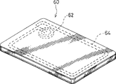
Fig. 6 illustrates the outward appearance according to the non-contact IC card 60 of further embodiment of this invention.
Fig. 7 illustrates an example of traditional non-contact IC card.
Fig. 8 A is that Fig. 8 B is the circuit diagram of IC-card 2 along the sectional view of VIIIA-VIIIA line intercepting among Fig. 7.
Realize best mode of the present invention
Fig. 1 illustrates the outward appearance that the non-contact IC card 30 of card is installed as circuit chip according to an embodiment of the invention.IC-card 30 is unicoil type IC-cards that use in the automatic classification of self-verifying, parcel in skiing field chair chute and railway.
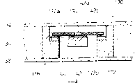
Fig. 2 is the sectional view along II-II line intercepting among Fig. 1.IC-card 30 has the structure that each layer is followed successively by superficial layer member 32 (this is first substrate), core component 34 and superficial layer member 36 (this is second substrate).Synthetic resin such as vinyl chloride, PET (polyethylene terephthalate) etc. is used as superficial layer member 32 and 36.Core component 34 is formed by synthetic resin.
The inside 38a of ceramic frame 38 forms a cavity.Elastic component 40 is a buffer component, is layered on the bottom of ceramic frame 38 inner 38a to contact with superficial layer member 32.Adhesive silicone rubber is used as elastic component 40.IC chip 42, promptly circuit chip is supported on the elastic component 40.In the present embodiment, the capacitor of the capacitor of resonant circuit and level and smooth power supply is loaded in the IC-card 42.
By ceramic frame 38 being embedded in 34 layers of the core components, can improve near flexural rigidity, torsional rigid and the compression rigidity of IC-card 30 ceramic frame 38 significantly.
Even on IC-card, apply stronger bending.Reverse or force of compression, the IC chip 42 that is positioned on the ceramic frame 38 inner 38a will can not produce very large deformation.Therefore, even the damage of IC chip 42 also seldom can take place when applying bending, reverse or oppressing power.In other words, can improve the reliability of IC-card 30.
Through the fixing IC chip 42 of elastic component 40, any bump that acts on the IC-card 30 will can not be directly delivered to IC chip 42.Therefore, can relax the damage of clashing into the IC chip 42 that causes.
In the present embodiment, two superficial layer members 32 and 36 thickness are 0.1mm, and the whole thickness of IC-card 30 is 0.768mm.IC chip 42 is that the length of side is that square, the thickness of 3mm is 0.25mm.The thickness of elastic component 40 is 0.118mm.The height of ceramic frame 38 is 0.568mm, comprises the coil 44 adjacent with upper surface 38b (hereinafter will describe).The interior diameter of ceramic frame 38 is to set like this, is about 0.2-0.3mm from the gap of the IC chip 42 of packing into.The overall diameter of ceramic frame 38 is about 23mm.Attention: the invention is not restricted to these sizes and material.
The coil 44 that forms antenna is set on the top of ceramic frame 38.Fig. 3 illustrates and unloads the IC-card 30 that desurfacing member 36 is watched from the V1 direction of Fig. 2.Coil 44 is to print or the loop metal wire that provides on the upper surface 38b of cylindrical ceramic framework 38 is provided to form.The terminal of coil 44 46 is connected to IC chip 42 by going between.
The upper surface 38b that coil 44 is arranged on ceramic frame 38 goes up the single element that allows prepared beforehand to connect IC chip 42, ceramic frame 38 and coil.Therefore, but the improvement of the workability by when preparation can reduce preparation cost.
Because the lead-in wire 46 that connects IC chip 42 and coil 44 is positioned at the scope of highly firm ceramic frame 38,, IC-card 30 unlikely takes place because of being bent the cut-out of the lead-in wire 46 that causes or disconnecting connection.Therefore, can improve the reliability of the non-contact IC card 30 that comprises coil 44.
By forming intensive aspect, can obtain high rigidity with pottery.Utilize the high-insulation of pottery, on ceramic frame 38, be provided with in the coil 44 and needn't use insulator.Coil 44 can be set directly on the ceramic frame 38 by means such as printings, to reduce manufacturing cost.
The operation of IC-card 30 is similar to the operation of traditional IC-card 2.More particularly, the electromagnetic wave that sends from reader/writer (writing/readout device, not shown) is installed in the resonant circuit (not shown) that coil 44 in the IC chip 42 and capacitor (not shown) form and receives.The electromagnetic wave that receives is corresponding to power source.The capacitor (not shown) of level and smooth power is installed in the IC chip 42.
The control module (not shown) that is arranged on the IC chip 42 is decoded to the information that is superimposed upon on the electromagnetic wave that obtains.Decoded information is sent back to.Can influence this response by the impedance that changes resonant circuit.Reader/writer can be discerned the content of response by the impedance variation that detects himself resonant circuit (not shown) according to the impedance variation of the resonant circuit of IC-card 3.
Therefore, the card that lacks power source can be launched in non-contacting mode/reception information.
Although above embodiment is configuration like this, promptly IC chip 42 is fixed on the superficial layer member 32 through elastic component 40, as shown in Figure 2,, IC chip 42 can directly be fixed on the superficial layer member 32, without elastic component 40.
Fig. 4 illustrates contactless IC card 50, and the sectional view of card is installed as the circuit chip of another embodiment of the present invention.The outward appearance of the structure of IC-card 50 is similar to the outward appearance of IC-card 30 (with reference to figure 1).Similar substantially from the V1 direction view of Fig. 4 to the view (with reference to figure 3) of IC-card 32.
Attention: the structure of ceramic frame 52 is different from the structure (with reference to figure 2) of the ceramic frame of IC-card 30 in the IC-card 50 as shown in Figure 4.More particularly, ceramic frame 52 is different from the ceramic frame 38 that is only formed by the cylindrical frame body, in ceramic frame 52, cylindrical part 52a (this is a frame body) and base section 52b (this is the flat board that arrives the bottom of cylindrical part 52a continuously that provides integratedly) are provided for it.
As shown in Figure 4, the configuration of IC chip 42 is directly to be fixed on the base section 52b of the caveli body 52c that cylindrical part 52a and base section 52b by ceramic frame 52 form.
By the base section 52b that arrives the bottom of cylindrical part 52a continuously is provided integratedly, can further improve the rigidity of ceramic frame 52.Therefore, even the relative increase of size of ceramic frame 52 also can guarantee required rigidity on in-plane (directions X among Fig. 1 and Y direction).Therefore, the diameter of coil 44 can be set greatlyyer.
As shown in Figure 4, IC chip module 54, promptly the circuit chip module by ceramic frame 52, be fixed to IC chip 42 on the ceramic frame 52, the lead-in wire 46 of the coil 44 that forms by printing or etching on ceramic frame 52 and connecting coil 44 and IC chip 42 forms.By such module is provided, but can improve workability in the preparation process, thereby allow to reduce manufacturing cost.
Although the configuration of present embodiment is that IC chip 42 directly is fixed on the base section 52b of ceramic frame 52,, elastic component 40 as shown in Figure 2 can be set between the base section 52b of IC chip 42 and ceramic frame 52.So, can the bump of abirritation on card.
Among the above embodiment each is configuration like this, promptly forms coil 44 in the upper surface of ceramic frame 38 or 52.Yet coil also can be arranged on lower end, side plane or the two ends of ceramic frame 38 or 52.In addition, ceramic frame 38 or 52 can be divided into two or more sections on thickness direction, make coil clamp in the middle of the ceramic frame that separates.
Although coil 44 is to be formed directly on ceramic frame 38 or 52 by printing or etching,, coil can be formed on the film of synthetic resin and the film that will be formed with coil is connected to ceramic frame 38 or 52 by etching etc.In addition, coil can twine ceramic frame 38 or 52.
Fig. 5 illustrates the sectional view of non-contact IC card 170, and this is that circuit chip is installed card according to another embodiment of the present invention.The outward appearance of IC-card 170 is similar to the outward appearance of IC-card 30.
As shown in Figure 5, be different from ceramic frame 38 (with reference to figure 2) in the IC-card 30 corresponding to the structure of the ceramic frame 172 of IC-card 170 center support bodys.More particularly, the outside of ceramic frame 172 is formed by single right cylinder, and as ceramic frame 38, its inboard forms with the step cylindrical shape.
As shown in Figure 5, the step part 172a of ceramic frame 172 is formed with a coil 44 that plays the antenna effect.The tread support membrane 174 that forms buffer component is arranged on the coil 44.Tread support membrane 174 is the film of synthetic resin that form as hollow cylinder, is applied with the printed wiring (not shown).The printed wiring of tread support membrane 174 and at the terminal 44a that is arranged on coil 44 ends by welding or protruding interconnection technique etc. (terminal combination technology) coupling.Therefore, tread support membrane 174 is bearing on the step part 172a of ceramic frame 172 with the coil 44 of the mode of shelving in the inner chamber body 172b of ceramic frame 172.
The terminal 42a of the terminal 44a of coil 44 and IC chip 42 realizes being electrically connected by the above-mentioned printed wiring that is arranged on the tread support membrane 174.
Adopt such structure, reliably the bump of mitigation on card.In being electrically connected of coil 44 and IC chip 42, do not need lead-in wire.Therefore, the thing that can not go between and disconnect connection or block.As shown in Figure 5, ceramic frame 172, coil 44, tread support membrane 174 and IC chip 42 form IC chip module 176, i.e. circuit chip module.Adopt this modular form, but can improve the workability of preparation, reduce manufacturing cost.
Present embodiment is configuration like this, and promptly tread support membrane 174 is connected by welding or protruding interconnection technique with the terminal 42a of IC chip 42.Yet tread support membrane 174 and IC chip 42 can be coupled through the anisotropic conductor (not shown).Anisotropic conductor is the conductor that only has electric conductivity in a direction, is bonding agent.Can adopt Anisolum (Hitachi chemical incorporated company) thermoset adhesive as anisotropic conductor.
Adopt this anisotropic conductor to allow the printed wiring of tread support membrane 174 to be electrically connected on the terminal 42a of IC chip 42.Because the anisotropic conductor that applies has been filled the gap between tread support membrane 174 and the IC chip 42, can increase the bond strength between tread support membrane 174 and the IC chip 42 significantly.By form the whole covering upper surface 42b of IC chip 42 with anisotropic conductor, can stop moisture to enter in the IC chip 42.Therefore, can prevent the corrosion of the aluminium wiring in the IC chip 42.
According to present embodiment, printed wiring is arranged on the tread support membrane 174 and sets up being electrically connected between coil 44 and the IC chip 42 through printed wiring.Yet coil 44 and IC chip 42 can be realized being electrically connected through the lead-in wire in Fig. 2 and 4 illustrated embodiments.Although the film of synthetic resin of hollow cylinder shape is used as buffer component, the shape of buffer component and material be not limited to above-mentioned these.
In addition, such just as IC-card among Fig. 6 60, coil 64 can be arranged on the outside of ceramic frame 62.Such structure allows coil 64 increased in size, and does not increase the size of ceramic frame 62.Therefore, even when the distance of leaving reader/writer is big, also can launch/reception information.
In each above-mentioned embodiment, the right cylinder that adopts the cylinder of break-through or have a bottom is as intensive aspect.Yet the cylindrical outside or inboard structure are not limited to cylindrical shape.For example, can adopt the tubular form of rectangle as intensive aspect.In addition, intensive aspect is not limited to cylindrical form, for example, can adopt flat type.In addition, can provide a plurality of intensive aspects, for example, can an intensive aspect respectively be set upper and lower, thereby in the middle of circuit chip is added in.
In each above-mentioned embodiment, intensive aspect is formed by pottery.Yet, can adopt pottery material in addition, as long as this material is hard.For example, can adopt such as stainless metal material or hard synthetic resin etc.
In each above-mentioned embodiment, the capacitor that the capacitor of resonant circuit and power are level and smooth is contained in the IC chip 42.Yet these capacitors not necessarily are contained in the IC chip 42.In this case, IC chip 42 and capacitor are installed on the fin, and this fin is installed in ceramic frame 38 or 52, shown in Fig. 8 A.In the embodiment of Fig. 5, capacitor can be installed on the tread support membrane 174.
Above-described each embodiment exemplifies for the present invention applies to a coil form contactless IC card.Yet the present invention also can be applicable to so-called a plurality of coil form contactless IC card.In addition, the present invention can be applied to the contact-type IC-card except that the non-contact type IC-card.Have, the present invention can be applicable to be equipped with entire circuit module and the whole card and the IC-card of circuit chip again.Here, card is meant the member that is essentially the plane, as credit card, commutation ticket, railway Go-as-you-please Ticket etc.
Claims (24)
1. the circuit chip that circuit chip is installed is installed card, it is characterized in that comprising at described card near intensive aspect and antenna that utilizes electromagnetic wave to communicate that is arranged on the described intensive aspect of the rigidity that an improvement is blocking the circuit chip.
2. circuit chip as claimed in claim 1 is installed card, it is characterized in that: described intensive aspect comprises a framework that is arranged in perpendicular to the in-plane of the thickness direction of card around described circuit chip.
3. circuit chip as claimed in claim 2 is installed card, and it is characterized in that: described intensive aspect comprises a planar plate members, it on thickness direction, cover described framework around cavity at least one side and
Described circuit chip is arranged in described planar plate members and the formed cavity that caves in substantially of framework.
4. circuit chip as claimed in claim 2 is installed card, and it is characterized in that: described circuit chip is bearing in the card through buffer component, has alleviated collision.
5. circuit chip as claimed in claim 4 is installed card, and it is characterized in that: described circuit chip is bearing in the card in the mode of shelving through described buffer component.
6. circuit chip as claimed in claim 1 is installed card, it is characterized in that: described card is that the contact-type circuit chip is installed card, and it carries out telecommunication by contact.
7. circuit chip as claimed in claim 1 is installed card, it is characterized in that: described card is that the non-contact type circuit chip is installed card, and it communicates in the non-contacting mode of electricity.
8. circuit chip as claimed in claim 4 is installed card, is installed in the non-contact type circuit chip that communicates in electricity noncontact mode and installs in the card, it is characterized in that: an antenna that utilizes electromagnetic wave to communicate is set on described buffer component.
9. circuit chip as claimed in claim 8 is installed card, and it is characterized in that: described antenna is an annular metal cord that is fixed on described intensive aspect or the described buffer component.
10. the circuit chip that circuit chip is installed is installed card, it is characterized in that it comprises:
First substrate,
Be arranged in the intensive aspect on described first substrate, on the thickness direction of card, a through hole arranged,
Be arranged in second substrate on the described intensive aspect,
Be arranged in the buffer component on described first substrate of described through hole,
Be arranged on the described buffer component of described through hole circuit chip and
Outside and be arranged in core component between described first substrate and described second substrate at described intensive aspect.
11. the circuit chip that circuit chip is installed is installed card, it is characterized in that it comprises:
First substrate,
Be arranged in the intensive aspect on described first substrate, on the thickness direction of card, a recessed openings that makes progress arranged,
Be arranged in second substrate on the described intensive aspect,
Be arranged in the buffer component on described first substrate in the described through hole,
Be arranged on the lower surface of recess described in the described recess circuit chip and
Be arranged in described intensive aspect outside and the core component between described first and second substrates.
12. the circuit chip that circuit chip is installed is installed card, it is characterized in that it comprises:
First substrate,
Be arranged in the intensive aspect on described first substrate, on the top part of card, a through hole arranged on the thickness direction,
Be arranged in second substrate on the described intensive aspect,
By the buffer component of the described intensive aspect supporting that is in the state of shelving in the described through hole,
By the circuit chip of the described buffer component supporting that is in the state of shelving in the described through hole and
Be arranged in the core component between described intensive aspect outside and described first and second substrate.
13. circuit chip as claimed in claim 10 is installed card, it is characterized in that: comprise one by the annular metal cord antenna that form and that be electrically connected with described circuit chip that is fixed on the described intensive aspect.
14. circuit chip as claimed in claim 10 is installed card, it is characterized in that: comprise one by the annular metal cord antenna that form and that be electrically connected with described circuit chip that is fixed on the described buffer component.
15. circuit chip as claimed in claim 1 is installed card, it is characterized in that: described intensive aspect is formed by pottery.
16. a configuration circuit chip is installed the circuit chip module of card, it is characterized in that:
The circuit chip and the improvement that are installed in the card are coupled at the intensive aspect of the rigidity of the described circuit chip place card of packing into integratedly,
Described intensive aspect comprise one be arranged in perpendicular to the in-plane of thickness direction of card around the framework institute of described circuit chip around cavity and one on thickness direction covering by described frame loops around the planar plate members of at least one side of cavity,
Described circuit chip is arranged in the cavity that caves in substantially that is formed by described planar plate members and framework.
17. a configuration circuit chip is installed the circuit chip module of card, it is characterized in that: the circuit chip and the improvement that are installed in the card are coupled at the intensive aspect of the rigidity of the described circuit chip place card of packing into integratedly,
Described circuit chip through a buffer component that alleviate to collide to shelve state support in card.
18. one kind is configured to the circuit chip module that non-contact type circuit chip that electricity noncontact mode communicates is installed card, it is characterized in that: the circuit chip and the improvement that are installed in the card are coupled at the intensive aspect of the rigidity of the described circuit chip place card of packing into integratedly
The antenna that utilizes electromagnetic wave to communicate is arranged on the described intensive aspect.
19. one kind is configured to the circuit chip module that non-contact type circuit chip that electricity noncontact mode communicates is installed card, it is characterized in that: be installed in the circuit chip in the card and improve the buffer component that collides between the two at the intensive aspect and an alleviation of the rigidity of the described circuit chip place card of packing into and be coupled integratedly
The antenna that utilizes electromagnetic wave to communicate is arranged on the described buffer component.
20. circuit chip module as claimed in claim 18 is characterized in that: described antenna is an annular metal cord that is fixed on described intensive aspect or the described buffer component.
21. circuit chip module as claimed in claim 19 is characterized in that: described antenna is an annular metal cord that is fixed on described intensive aspect or the described buffer component.
22. circuit chip as claimed in claim 11 is installed card, it is characterized in that: comprise one by the annular metal cord antenna that form and that be electrically connected with described circuit chip that is fixed on the described intensive aspect.
23. circuit chip as claimed in claim 12 is installed card, it is characterized in that: comprise one by the annular metal cord antenna that form and that be electrically connected with described circuit chip that is fixed on the described intensive aspect.
24. circuit chip as claimed in claim 12 is installed card, it is characterized in that: comprise one by the annular metal cord antenna that form and that be electrically connected with described circuit chip that is fixed on the described buffer component.
Applications Claiming Priority (2)
| Application Number | Priority Date | Filing Date | Title |
|---|---|---|---|
| JP351359/96 | 1996-12-27 | ||
| JP35135996A JP4108779B2 (en) | 1996-12-27 | 1996-12-27 | Circuit chip mounted card and circuit chip module |
Publications (2)
| Publication Number | Publication Date |
|---|---|
| CN1241969A CN1241969A (en) | 2000-01-19 |
| CN1086346C true CN1086346C (en) | 2002-06-19 |
Family
ID=18416769
Family Applications (1)
| Application Number | Title | Priority Date | Filing Date |
|---|---|---|---|
| CN97181047A Expired - Fee Related CN1086346C (en) | 1996-12-27 | 1997-12-22 | Card mounted with circuit chip and circuit chip module |
Country Status (8)
| Country | Link |
|---|---|
| US (1) | US6478228B1 (en) |
| EP (2) | EP1514698B1 (en) |
| JP (1) | JP4108779B2 (en) |
| CN (1) | CN1086346C (en) |
| AU (1) | AU742524B2 (en) |
| CA (1) | CA2277181A1 (en) |
| DE (2) | DE69732719T2 (en) |
| WO (1) | WO1998029262A1 (en) |
Families Citing this family (38)
| Publication number | Priority date | Publication date | Assignee | Title |
|---|---|---|---|---|
| JP2001084343A (en) * | 1999-09-16 | 2001-03-30 | Toshiba Corp | Non-contact ic card and ic card communication system |
| EP1174821A1 (en) * | 2000-07-20 | 2002-01-23 | Sokymat S.A. | Transponder with reinforcing member |
| JP2002074298A (en) * | 2000-08-30 | 2002-03-15 | Fujitsu Ltd | Non-contact type ic card |
| US6923378B2 (en) * | 2000-12-22 | 2005-08-02 | Digimarc Id Systems | Identification card |
| JP2002278451A (en) * | 2001-03-16 | 2002-09-27 | Jr East Mechatronics Co Ltd | Label-like ic card for railroad |
| KR100411811B1 (en) * | 2001-04-02 | 2003-12-24 | 앰코 테크놀로지 코리아 주식회사 | Semiconductor package |
| JP2002342731A (en) * | 2001-05-16 | 2002-11-29 | Matsushita Electric Ind Co Ltd | Composite ic card |
| US7063264B2 (en) | 2001-12-24 | 2006-06-20 | Digimarc Corporation | Covert variable information on identification documents and methods of making same |
| ATE509326T1 (en) | 2001-12-18 | 2011-05-15 | L 1 Secure Credentialing Inc | MULTIPLE IMAGE SECURITY FEATURES FOR IDENTIFYING DOCUMENTS AND METHOD FOR PRODUCING THEM |
| US7793846B2 (en) | 2001-12-24 | 2010-09-14 | L-1 Secure Credentialing, Inc. | Systems, compositions, and methods for full color laser engraving of ID documents |
| US7728048B2 (en) | 2002-12-20 | 2010-06-01 | L-1 Secure Credentialing, Inc. | Increasing thermal conductivity of host polymer used with laser engraving methods and compositions |
| WO2003055638A1 (en) | 2001-12-24 | 2003-07-10 | Digimarc Id Systems, Llc | Laser etched security features for identification documents and methods of making same |
| US7694887B2 (en) | 2001-12-24 | 2010-04-13 | L-1 Secure Credentialing, Inc. | Optically variable personalized indicia for identification documents |
| AU2003221894A1 (en) | 2002-04-09 | 2003-10-27 | Digimarc Id Systems, Llc | Image processing techniques for printing identification cards and documents |
| US7824029B2 (en) | 2002-05-10 | 2010-11-02 | L-1 Secure Credentialing, Inc. | Identification card printer-assembler for over the counter card issuing |
| KR100467634B1 (en) * | 2002-07-16 | 2005-01-24 | 삼성에스디에스 주식회사 | Smart card and manufacturing method of the same |
| DE10232569A1 (en) * | 2002-07-18 | 2004-02-05 | Agfa-Gevaert Ag | identity card |
| US7804982B2 (en) | 2002-11-26 | 2010-09-28 | L-1 Secure Credentialing, Inc. | Systems and methods for managing and detecting fraud in image databases used with identification documents |
| US7712673B2 (en) | 2002-12-18 | 2010-05-11 | L-L Secure Credentialing, Inc. | Identification document with three dimensional image of bearer |
| DE102004008841A1 (en) * | 2003-03-12 | 2004-09-23 | Bundesdruckerei Gmbh | Security insert, to prevent forgery or tampering, at a book document e.g. a passport, has an integrated data carrier with a microchip which can be scanned without contact |
| EP1614064B1 (en) | 2003-04-16 | 2010-12-08 | L-1 Secure Credentialing, Inc. | Three dimensional data storage |
| JP4567988B2 (en) * | 2004-02-05 | 2010-10-27 | 株式会社日立製作所 | Paper-like RFID tag and manufacturing method thereof |
| JP4077442B2 (en) * | 2004-11-09 | 2008-04-16 | 東芝テック株式会社 | Wireless tag holding structure |
| EP1677232A1 (en) * | 2004-12-22 | 2006-07-05 | Trüb AG | Data carrier and method for manufacturing such a data carrier |
| JP4536552B2 (en) * | 2005-02-28 | 2010-09-01 | ケイ・アール・ディコーポレーション株式会社 | IC tag |
| NL1029985C2 (en) * | 2005-09-20 | 2007-03-21 | Sdu Identification Bv | Identity document with chip, e.g. ID card or driving license, includes buffer layer for preventing hairline cracks forming in plastic support |
| US7714535B2 (en) | 2006-07-28 | 2010-05-11 | Semiconductor Energy Laboratory Co., Ltd. | Power storage device |
| US8232621B2 (en) * | 2006-07-28 | 2012-07-31 | Semiconductor Energy Laboratory Co., Ltd. | Semiconductor device |
| US7838976B2 (en) * | 2006-07-28 | 2010-11-23 | Semiconductor Energy Laboratory Co., Ltd. | Semiconductor device having a semiconductor chip enclosed by a body structure and a base |
| DE202008010294U1 (en) | 2008-08-01 | 2008-10-16 | Flexo-Print Bedienfelder Gmbh | transponder |
| CN102332102A (en) * | 2010-07-13 | 2012-01-25 | 凸版印刷(上海)有限公司 | Contactless card with sheet metal and realization method thereof |
| CN203279336U (en) * | 2013-04-27 | 2013-11-06 | 中兴通讯股份有限公司 | Inner heat dissipation terminal |
| EP3146476A4 (en) | 2014-05-22 | 2017-12-13 | Composecure LLC | Transaction and id cards having selected texture and coloring |
| JP6367661B2 (en) * | 2014-09-19 | 2018-08-01 | マクセルホールディングス株式会社 | IC module |
| US10783422B2 (en) | 2014-11-03 | 2020-09-22 | Composecure, Llc | Ceramic-containing and ceramic composite transaction cards |
| CN112836778A (en) * | 2014-11-03 | 2021-05-25 | 安全创造有限责任公司 | Transaction card containing ceramic and ceramic composite material |
| DE102017122052A1 (en) * | 2017-09-22 | 2019-03-28 | Schreiner Group Gmbh & Co. Kg | RFID tag with protection of the RFID function |
| FR3073307B1 (en) * | 2017-11-08 | 2021-05-28 | Oberthur Technologies | SECURITY DEVICE SUCH AS A CHIP CARD |
Citations (4)
| Publication number | Priority date | Publication date | Assignee | Title |
|---|---|---|---|---|
| JPS62236793A (en) * | 1986-04-07 | 1987-10-16 | 松下電子工業株式会社 | Integrated circuit card |
| JPS6440397A (en) * | 1987-08-07 | 1989-02-10 | Dainippon Printing Co Ltd | Portable electronic device |
| JPH07200766A (en) * | 1993-12-28 | 1995-08-04 | Omron Corp | Electronic card |
| JPH08282167A (en) * | 1995-04-13 | 1996-10-29 | Rohm Co Ltd | Ic card |
Family Cites Families (6)
| Publication number | Priority date | Publication date | Assignee | Title |
|---|---|---|---|---|
| US4921160A (en) * | 1988-02-29 | 1990-05-01 | American Telephone And Telegraph Company | Personal data card and method of constructing the same |
| JP2709223B2 (en) | 1992-01-30 | 1998-02-04 | 三菱電機株式会社 | Non-contact portable storage device |
| US5581445A (en) | 1994-02-14 | 1996-12-03 | Us3, Inc. | Plastic integrated circuit card with reinforcement structure for protecting integrated circuit module |
| CN1054573C (en) * | 1994-09-22 | 2000-07-19 | 罗姆股份有限公司 | Non-contact type IC card and method of manufacturing same |
| DE4437844C2 (en) * | 1994-10-22 | 2001-03-08 | Cubit Electronics Gmbh | Contactless data carrier and method for its production |
| US5955723A (en) * | 1995-05-03 | 1999-09-21 | Siemens Aktiengesellschaft | Contactless chip card |
-
1996
- 1996-12-27 JP JP35135996A patent/JP4108779B2/en not_active Expired - Fee Related
-
1997
- 1997-12-22 CN CN97181047A patent/CN1086346C/en not_active Expired - Fee Related
- 1997-12-22 DE DE69732719T patent/DE69732719T2/en not_active Expired - Fee Related
- 1997-12-22 DE DE69738891T patent/DE69738891D1/en not_active Expired - Lifetime
- 1997-12-22 EP EP04028035A patent/EP1514698B1/en not_active Expired - Lifetime
- 1997-12-22 EP EP97949217A patent/EP1013472B1/en not_active Expired - Lifetime
- 1997-12-22 AU AU78894/98A patent/AU742524B2/en not_active Ceased
- 1997-12-22 WO PCT/JP1997/004771 patent/WO1998029262A1/en active IP Right Grant
- 1997-12-22 CA CA002277181A patent/CA2277181A1/en not_active Abandoned
- 1997-12-22 US US09/331,190 patent/US6478228B1/en not_active Expired - Fee Related
Patent Citations (4)
| Publication number | Priority date | Publication date | Assignee | Title |
|---|---|---|---|---|
| JPS62236793A (en) * | 1986-04-07 | 1987-10-16 | 松下電子工業株式会社 | Integrated circuit card |
| JPS6440397A (en) * | 1987-08-07 | 1989-02-10 | Dainippon Printing Co Ltd | Portable electronic device |
| JPH07200766A (en) * | 1993-12-28 | 1995-08-04 | Omron Corp | Electronic card |
| JPH08282167A (en) * | 1995-04-13 | 1996-10-29 | Rohm Co Ltd | Ic card |
Also Published As
| Publication number | Publication date |
|---|---|
| CA2277181A1 (en) | 1998-07-09 |
| US6478228B1 (en) | 2002-11-12 |
| EP1013472A1 (en) | 2000-06-28 |
| CN1241969A (en) | 2000-01-19 |
| WO1998029262A1 (en) | 1998-07-09 |
| EP1514698B1 (en) | 2008-08-06 |
| EP1514698A2 (en) | 2005-03-16 |
| DE69738891D1 (en) | 2008-09-18 |
| JP4108779B2 (en) | 2008-06-25 |
| EP1013472B1 (en) | 2005-03-09 |
| EP1013472A4 (en) | 2000-08-30 |
| DE69732719T2 (en) | 2006-04-13 |
| AU742524B2 (en) | 2002-01-03 |
| DE69732719D1 (en) | 2005-04-14 |
| EP1514698A3 (en) | 2005-03-30 |
| JPH10193847A (en) | 1998-07-28 |
| AU7889498A (en) | 1998-07-31 |
Similar Documents
| Publication | Publication Date | Title |
|---|---|---|
| CN1086346C (en) | Card mounted with circuit chip and circuit chip module | |
| CN1080652C (en) | Card mounted with circuit chip and circuit chip module | |
| CN1068546C (en) | Semiconductor device | |
| CN1143381C (en) | Chip card module, combined chip card containing the module, and manufacturing process | |
| CN1266763C (en) | Semiconductor module and production method thereof and module for IC card etc. | |
| CN1116654C (en) | Wireless module and wireless card | |
| CN1146828C (en) | Method for producing contactless electronic chip card | |
| CN1054573C (en) | Non-contact type IC card and method of manufacturing same | |
| CN1144155C (en) | IC module and IC card | |
| EP1045443A3 (en) | Semiconductor device and manufacturing method thereof | |
| CN1160449A (en) | Support element | |
| US20140042230A1 (en) | Chip card module with separate antenna and chip card inlay using same | |
| CN1238856A (en) | Chip module and manufacturing process thereof | |
| CN1858907A (en) | Semiconductor device and fabrication method thereof | |
| CN1185232A (en) | Semiconductor assembly | |
| CN1726591A (en) | Electronic device and method of manufacturing same | |
| CN101385402A (en) | Circuit board and process for producing the same | |
| CN110463168A (en) | Configurable encapsulation sensor module and its manufacturing method | |
| CN1295725A (en) | Aatenna means, method for its manufacturing and hand-held radio communication device | |
| CN1610194A (en) | IC card | |
| CN1351733A (en) | Method for the production of a portable integrated circuit electronic device comprising a low-cost dielectric | |
| US20030085454A1 (en) | Chip card and production process | |
| CN100401488C (en) | Chip module with bond-wire connections with small loop height | |
| GB2312089A (en) | Contactless data carrier | |
| US20200365330A1 (en) | Tantalum capacitor |
Legal Events
| Date | Code | Title | Description |
|---|---|---|---|
| C06 | Publication | ||
| PB01 | Publication | ||
| C10 | Entry into substantive examination | ||
| SE01 | Entry into force of request for substantive examination | ||
| C10 | Entry into substantive examination | ||
| SE01 | Entry into force of request for substantive examination | ||
| C14 | Grant of patent or utility model | ||
| GR01 | Patent grant | ||
| C19 | Lapse of patent right due to non-payment of the annual fee | ||
| CF01 | Termination of patent right due to non-payment of annual fee |