CN108350320B - Adhesive composition and structure - Google Patents
Adhesive composition and structure Download PDFInfo
- Publication number
- CN108350320B CN108350320B CN201680062847.XA CN201680062847A CN108350320B CN 108350320 B CN108350320 B CN 108350320B CN 201680062847 A CN201680062847 A CN 201680062847A CN 108350320 B CN108350320 B CN 108350320B
- Authority
- CN
- China
- Prior art keywords
- mass
- group
- adhesive composition
- silane compound
- circuit
- Prior art date
- Legal status (The legal status is an assumption and is not a legal conclusion. Google has not performed a legal analysis and makes no representation as to the accuracy of the status listed.)
- Active
Links
Images

Classifications
-
- C—CHEMISTRY; METALLURGY
- C09—DYES; PAINTS; POLISHES; NATURAL RESINS; ADHESIVES; COMPOSITIONS NOT OTHERWISE PROVIDED FOR; APPLICATIONS OF MATERIALS NOT OTHERWISE PROVIDED FOR
- C09J—ADHESIVES; NON-MECHANICAL ASPECTS OF ADHESIVE PROCESSES IN GENERAL; ADHESIVE PROCESSES NOT PROVIDED FOR ELSEWHERE; USE OF MATERIALS AS ADHESIVES
- C09J4/00—Adhesives based on organic non-macromolecular compounds having at least one polymerisable carbon-to-carbon unsaturated bond ; adhesives, based on monomers of macromolecular compounds of groups C09J183/00 - C09J183/16
-
- C—CHEMISTRY; METALLURGY
- C09—DYES; PAINTS; POLISHES; NATURAL RESINS; ADHESIVES; COMPOSITIONS NOT OTHERWISE PROVIDED FOR; APPLICATIONS OF MATERIALS NOT OTHERWISE PROVIDED FOR
- C09J—ADHESIVES; NON-MECHANICAL ASPECTS OF ADHESIVE PROCESSES IN GENERAL; ADHESIVE PROCESSES NOT PROVIDED FOR ELSEWHERE; USE OF MATERIALS AS ADHESIVES
- C09J11/00—Features of adhesives not provided for in group C09J9/00, e.g. additives
- C09J11/02—Non-macromolecular additives
- C09J11/04—Non-macromolecular additives inorganic
-
- C—CHEMISTRY; METALLURGY
- C09—DYES; PAINTS; POLISHES; NATURAL RESINS; ADHESIVES; COMPOSITIONS NOT OTHERWISE PROVIDED FOR; APPLICATIONS OF MATERIALS NOT OTHERWISE PROVIDED FOR
- C09J—ADHESIVES; NON-MECHANICAL ASPECTS OF ADHESIVE PROCESSES IN GENERAL; ADHESIVE PROCESSES NOT PROVIDED FOR ELSEWHERE; USE OF MATERIALS AS ADHESIVES
- C09J11/00—Features of adhesives not provided for in group C09J9/00, e.g. additives
- C09J11/02—Non-macromolecular additives
- C09J11/06—Non-macromolecular additives organic
-
- C—CHEMISTRY; METALLURGY
- C09—DYES; PAINTS; POLISHES; NATURAL RESINS; ADHESIVES; COMPOSITIONS NOT OTHERWISE PROVIDED FOR; APPLICATIONS OF MATERIALS NOT OTHERWISE PROVIDED FOR
- C09J—ADHESIVES; NON-MECHANICAL ASPECTS OF ADHESIVE PROCESSES IN GENERAL; ADHESIVE PROCESSES NOT PROVIDED FOR ELSEWHERE; USE OF MATERIALS AS ADHESIVES
- C09J9/00—Adhesives characterised by their physical nature or the effects produced, e.g. glue sticks
- C09J9/02—Electrically-conducting adhesives
-
- H—ELECTRICITY
- H01—ELECTRIC ELEMENTS
- H01B—CABLES; CONDUCTORS; INSULATORS; SELECTION OF MATERIALS FOR THEIR CONDUCTIVE, INSULATING OR DIELECTRIC PROPERTIES
- H01B1/00—Conductors or conductive bodies characterised by the conductive materials; Selection of materials as conductors
- H01B1/20—Conductive material dispersed in non-conductive organic material
- H01B1/22—Conductive material dispersed in non-conductive organic material the conductive material comprising metals or alloys
-
- H—ELECTRICITY
- H05—ELECTRIC TECHNIQUES NOT OTHERWISE PROVIDED FOR
- H05K—PRINTED CIRCUITS; CASINGS OR CONSTRUCTIONAL DETAILS OF ELECTRIC APPARATUS; MANUFACTURE OF ASSEMBLAGES OF ELECTRICAL COMPONENTS
- H05K1/00—Printed circuits
- H05K1/02—Details
- H05K1/14—Structural association of two or more printed circuits
-
- H—ELECTRICITY
- H05—ELECTRIC TECHNIQUES NOT OTHERWISE PROVIDED FOR
- H05K—PRINTED CIRCUITS; CASINGS OR CONSTRUCTIONAL DETAILS OF ELECTRIC APPARATUS; MANUFACTURE OF ASSEMBLAGES OF ELECTRICAL COMPONENTS
- H05K3/00—Apparatus or processes for manufacturing printed circuits
- H05K3/10—Apparatus or processes for manufacturing printed circuits in which conductive material is applied to the insulating support in such a manner as to form the desired conductive pattern
- H05K3/20—Apparatus or processes for manufacturing printed circuits in which conductive material is applied to the insulating support in such a manner as to form the desired conductive pattern by affixing prefabricated conductor pattern
-
- H—ELECTRICITY
- H05—ELECTRIC TECHNIQUES NOT OTHERWISE PROVIDED FOR
- H05K—PRINTED CIRCUITS; CASINGS OR CONSTRUCTIONAL DETAILS OF ELECTRIC APPARATUS; MANUFACTURE OF ASSEMBLAGES OF ELECTRICAL COMPONENTS
- H05K3/00—Apparatus or processes for manufacturing printed circuits
- H05K3/30—Assembling printed circuits with electric components, e.g. with resistor
- H05K3/32—Assembling printed circuits with electric components, e.g. with resistor electrically connecting electric components or wires to printed circuits
Abstract
An adhesive composition comprising: a1 st silane compound having a radically polymerizable functional group, a2 nd silane compound reacted with the 1 st silane compound, a radically polymerizable compound (excluding a compound corresponding to the 1 st silane compound), and a peroxide having a 1-minute half-life temperature of 120 ℃ or less.
Description
Technical Field
The present invention relates to an adhesive composition and a structure.
Background
In semiconductor devices and liquid crystal display devices (display devices), various adhesives have been conventionally used for the purpose of bonding various members in the devices. The properties required of the adhesive include adhesiveness, heat resistance, and reliability in a high-temperature and high-humidity state. As the adherend used for adhesion, a printed wiring board, an organic base material (polyimide base material, etc.), a metal (titanium, copper, aluminum, etc.), ITO, IZO, IGZO, SiN, or the like is usedx、SiO2For example, the molecular design of the adhesive is required for the substrate in the surface state depending on each adherend.
Conventionally, thermosetting resins (epoxy resins, acrylic resins, and the like) exhibiting high adhesiveness and high reliability have been used for adhesives for semiconductor elements and adhesives for liquid crystal display elements. As a component of an adhesive using an epoxy resin, an epoxy resin and a latent curing agent that generates a cationic species or an anionic species reactive with the epoxy resin by heat or light are generally used. The latent curing agent is an important factor for determining the curing temperature and curing speed, and various compounds are used from the viewpoint of storage stability at room temperature and curing speed at heating. In an actual process, the desired adhesiveness is obtained by curing under curing conditions of, for example, 170 to 250 ℃ for 10 seconds to 3 hours.
In recent years, with the high integration of semiconductor elements and the high definition of liquid crystal display elements, the pitches between elements and between wirings have become narrow, and there is a concern that heat during curing may adversely affect peripheral members. Further, for cost reduction, it is necessary to increase the production amount, and low-temperature (90 to 170 ℃) and short-time (within 1 hour, preferably within 10 seconds, and more preferably within 5 seconds) bonding, in other words, low-temperature short-time curing (low-temperature rapid curing) bonding is required. It is known that in order to achieve such low-temperature short-time curing, a heat latent catalyst having low activation energy needs to be used, but it is very difficult to achieve storage stability at around room temperature.
Therefore, in recent years, attention has been paid to radical-curable adhesives and the like using a combination of a (meth) acrylate derivative and a peroxide as a radical polymerization initiator. The radical curing system is a curing system in which both low-temperature short-time curing and storage stability (for example, storage stability at around room temperature) are compatible because a radical as a reactive species is very reactive and can be cured in a short time, and because a peroxide stably exists at a temperature of not higher than the decomposition temperature of a radical polymerization initiator. For example, a radical curable adhesive composition containing a silane compound (e.g., a silane coupling agent) having a radical polymerizable functional group ((meth) acryloyl group, vinyl group, etc.) is known (see, for example, patent document 1 below).
Documents of the prior art
Patent document
Patent document 1: japanese patent laid-open publication No. 2013-191625
Patent document 2: japanese patent laid-open publication No. 2006-22231
Patent document 3: international publication No. 2009/063827
Disclosure of Invention
Problems to be solved by the invention
However, when a conventional adhesive composition (mixture) containing a silane compound having a radical polymerizable functional group is stored, the characteristics of the silane compound are significantly deteriorated, and the adhesiveness of the adhesive composition is lowered. Therefore, improvement in storage stability is required for conventional radical-curable adhesive compositions.
The purpose of the present invention is to provide an adhesive composition having excellent storage stability, and a structure using the same.
Means for solving the problems
The present inventors speculate as follows regarding the main cause of deterioration in the properties of the silane compound in the conventional adhesive composition. That is, when a polymerization reaction is initiated by another initiator different from the silane compound during storage of the adhesive composition, the silane compound is incorporated into the polymerization reaction and incorporated into the constituent material (such as resin) of the adhesive composition. It is presumed that: the number of molecules that can act on the interface between the adhesive composition and the adherend is reduced, and thus the characteristics are deteriorated.
The present inventors have also found that the above-mentioned property deterioration is particularly remarkable when a peroxide having a high activity and a half-life temperature of 1 minute of 120 ℃ or less is used in a radical polymerization (e.g., (meth) acrylate radical) adhesive composition (that is, when low-temperature short-time curing of 130 ℃ for 5 seconds, which is required to be expanded in recent years).
The present inventors have conducted intensive studies to improve the storage stability (life characteristics), and as a result, have found that the storage stability of an adhesive composition containing a radical polymerizable compound and a peroxide having a 1-minute half-life temperature of 120 ℃ or less is remarkably improved when a1 st silane compound having a radical polymerizable functional group and a2 nd silane compound reacted with the 1 st silane compound are used in combination.
The adhesive composition of the present invention comprises: a1 st silane compound having a radically polymerizable functional group, a2 nd silane compound reacted with the 1 st silane compound, a radically polymerizable compound (excluding a compound corresponding to the 1 st silane compound), and a peroxide having a 1-minute half-life temperature of 120 ℃ or less.
The adhesive composition of the present invention has superior storage stability compared to conventional adhesive compositions. Such an adhesive composition can suppress the deterioration of the adhesiveness of the adhesive composition with time during storage.
The present inventors speculate as follows regarding the main reason for obtaining such an effect. That is, by the presence of the 1 st silane compound having a radical polymerizable functional group and the 2 nd silane compound which reacts with the 1 st silane compound in the adhesive composition, even when the 1 st silane compound is radical polymerized and incorporated into a polymer during storage, the 2 nd silane compound can be crosslinked with the 1 st silane compound and an adherend in the polymer to maintain the adhesiveness between the adhesive composition or a cured product thereof and the adherend.
In addition, in the above-mentioned patent document 2, a silane coupling agent is used in the radical curing system for the purpose of improving the adhesion at the initial stage of connection and the adhesion after the reliability test. However, in patent document 2, a peroxide having a high 1-minute half-life temperature of 125 ℃ (in other words, a peroxide having high stability) is used, and the present inventors have conducted studies and found that the effect of a silane coupling agent on the storage stability may not be sufficiently confirmed. Further, patent document 2 discloses that the connection conditions are 150 ℃ for 10 seconds, and it is found that the curing reaction may not sufficiently occur under the connection conditions of 130 ℃ for 5 seconds, which is required in recent years. On the other hand, the adhesive composition of the present invention can be cured at a low temperature for a short time (within 1 hour, preferably within 10 seconds, more preferably within 5 seconds, at 90 to 170 ℃), and can be sufficiently cured even under the connection conditions of 130 ℃ and 5 seconds, etc.
The functional group of the 1 st silane compound preferably contains at least one selected from the group consisting of a (meth) acryloyl group and a vinyl group. The 2 nd silane compound preferably has an epoxy group.
The adhesive composition of the present invention may further contain conductive particles.
The adhesive composition of the present invention can be used for circuit connection (adhesive composition for circuit connection).
The structure of the present invention includes the adhesive composition or the cured product thereof.
The structure of the present invention may be configured to include: a first circuit member having a first circuit electrode, a second circuit member having a second circuit electrode, and a circuit connecting member disposed between the first circuit member and the second circuit member; the first circuit electrode and the second circuit electrode are electrically connected, and the circuit connecting member includes the adhesive composition or a cured product thereof.
ADVANTAGEOUS EFFECTS OF INVENTION
According to the present invention, an adhesive composition having superior storage stability compared to conventional ones and a structure using the same can be provided.
The present invention can provide an application of the adhesive composition or a cured product thereof to a structure or a production thereof. The present invention can provide an application of the adhesive composition or a cured product thereof to circuit connection. The present invention can provide an application of the adhesive composition or a cured product thereof to a circuit connecting structure or a production thereof.
Drawings
Fig. 1 is a schematic cross-sectional view showing one embodiment of the structure of the present invention.
Fig. 2 is a schematic cross-sectional view showing another embodiment of the structure of the present invention.
Detailed Description
The present invention will be described below with reference to embodiments, but the present invention is not limited to these embodiments at all.
In the present specification, "(meth) acrylate" means at least one of an acrylate and a corresponding methacrylate. The same applies to other similar expressions such as "(meth) acryloyl group", "meth) acrylic acid", and the like. The following materials may be used alone or in combination of two or more unless otherwise specified. The content of each component in the composition means the total amount of a plurality of substances present in the composition unless otherwise specified, when a plurality of substances corresponding to each component are present in the composition. The numerical range represented by the term "to" represents a range including the numerical values recited before and after the term "to" as the minimum value and the maximum value, respectively. "a or B" may include either or both of a and B. The term "ordinary temperature" means 25 ℃.
In the numerical ranges recited in the present specification, the upper limit or the lower limit of a numerical range in one stage may be replaced with the upper limit or the lower limit of a numerical range in another stage. In the numerical ranges described in the present specification, the upper limit or the lower limit of the numerical range may be replaced with the values shown in the examples.
< adhesive composition >
The adhesive composition of the present embodiment contains a silane compound, a radical polymerizable compound (radical polymerizable material), and a curing agent. The adhesive composition of the present embodiment contains, as silane compounds, a1 st silane compound having a radically polymerizable functional group (a functional group participating in a radical polymerization reaction of a curing system, a functional group polymerizable in a radical polymerization system), and a2 nd silane compound reacted with the 1 st silane compound (except for a compound corresponding to the 1 st silane compound). The adhesive composition of the present embodiment contains a peroxide having a 1-minute half-life temperature of 120 ℃ or less as the curing agent. The adhesive composition of the present embodiment is a radical curing (radical polymerization) adhesive composition. The adhesive composition of the present embodiment can be suitably used as an adhesive composition for circuit connection. Hereinafter, each component will be described.
(silane Compound)
The adhesive composition of the present embodiment contains a1 st silane compound having a radical polymerizable functional group and a2 nd silane compound that reacts with the 1 st silane compound. The 2 nd silane compound is a compound which is not equivalent to the 1 st silane compound and does not have a radical polymerizable functional group. The silane compound may also be a silane coupling agent.
Examples of the radical polymerizable functional group include groups having an ethylenically unsaturated bond such as a (meth) acryloyl group, a vinyl group, a styryl group, and a maleimide group. From the viewpoint of obtaining more excellent storage stability and adhesiveness, the radical polymerizable functional group is preferably at least one selected from the group consisting of a (meth) acryloyl group and a vinyl group, and more preferably a (meth) acryloyl group.
The 2 nd silane compound may also have a functional group that does not participate in radical polymerization. Examples of the functional group that does not participate in the radical polymerization reaction include an alkyl group, a phenyl group, an alkoxysilyl group, an amino group, an alkylamino group (e.g., a methylamino group), a benzylamino group, a phenylamino group, a cycloalkylamino group (e.g., a cyclohexylamino group), a morpholinyl group, a piperazinyl group, an isocyanate group, an imidazolyl group, a ureido group, a dialkylamino group (e.g., a dimethylamino group), and an epoxy group. The epoxy group may be included in an epoxy group-containing group (epoxy group-containing group) such as a glycidyl group, glycidyloxy group, etc. From the viewpoint of obtaining more excellent storage stability, the 2 nd silane compound preferably has at least one selected from the group consisting of an alkyl group and an epoxy group, and more preferably has an epoxy group.
As the silane compound, a compound represented by the following general formula (I) can be used. The compound represented by the formula (I) can be synthesized, for example, by reacting an organochlorosilane with an alcohol.
[ solution 1]
X-CsH2s-Si〔R1〕m〔OR2〕3-m…(1)
[ wherein X represents an organic group, R1And R2Each independently represents an alkyl group, m represents an integer of 0 to 2, and s represents an integer of 0 or more. At R1When there are plural, each R1May be the same or different from each other. At R2When there are plural, each R2May be the same or different from each other. R1、R2And CsH2sEach may also be branched.]
Examples of the organic group X include a group having an ethylenically unsaturated bond (a group having an ethylenically unsaturated bond), a group having a nitrogen atom (a group having a nitrogen atom), a group having a sulfur atom (a group having a sulfur atom), and an epoxy group. Examples of the ethylenically unsaturated bond-containing group include a (meth) acryloyl group, a vinyl group, and a styryl group. Examples of the nitrogen atom-containing group include an amino group, a mono-substituted amino group, a di-substituted amino group, an isocyanate group, an imidazole group, a urea group, and a maleimide group. Examples of the mono-substituted amino group include an alkylamino group (e.g., methylamino group), a benzylamino group, a phenylamino group, and a cycloalkylamino group (e.g., cyclohexylamino group). Examples of the disubstituted amino group include an acyclic disubstituted amino group and a cyclic disubstituted amino group. Examples of the acyclic disubstituted amino group include a dialkylamino group (e.g., dimethylamino group). Examples of the cyclic disubstituted amino group include a morpholinyl group and a piperazinyl group. Examples of the group containing a sulfur atom include a mercapto group and the like. The epoxy group may be included in an epoxy group-containing group (epoxy group-containing group) such as a glycidyl group, glycidyloxy group, etc. The (meth) acryloyl group may also be contained in the (meth) acryloyloxy group.
R1And R2The number of carbon atoms of the alkyl group is, for example, 1 to 20. Specific examples of the alkyl group include a methyl group, an ethyl group, a propyl group, a butyl group, a pentyl group, a hexyl group, a heptyl group, an octyl group, a nonyl group, a decyl group, an undecyl group, a dodecyl group, a tridecyl group, a tetradecyl group, a pentadecyl group, a hexadecyl group, a heptadecyl group, an octadecyl group, a nonadecyl group, and an eicosyl group. As R1And R2The above-mentioned structural isomers of the alkyl group can be used. From the viewpoint that the alkoxysilane moiety is less likely to cause steric hindrance when reacting with the adherend, and that more excellent adhesiveness to the adherend is obtained, R1The number of carbon atoms of the alkyl group(s) is preferably 1 to 10, more preferably 1 to 5. From the viewpoint of obtaining more excellent adhesiveness to an adherend, R2The number of carbon atoms of the alkyl group(s) is preferably 1 to 10, more preferably 1 to 5.
m is an integer of 0 to 2. M is preferably 0 to 1, more preferably 0, from the viewpoint of being less likely to cause steric hindrance when the alkoxysilane moiety reacts with the adherend, and obtaining more excellent adhesiveness to the adherend. s is an integer greater than or equal to 0. From the viewpoint of obtaining more excellent storage stability, s is preferably an integer of 1 to 20, and more preferably an integer of 1 to 10.
Examples of the 1 st silane compound include (meth) acryloyloxyalkyltrialkoxysilanes, (meth) acryloyloxydialkyldialkoxysilanes, (meth) acryloyloxytrialkylalkoxysilanes, alkenyltrialkoxysilanes, styryltrialkoxysilanes, styrylalkyltrialkoxysilanes, and the like. The 1 st silane compound is preferably at least one selected from the group consisting of (meth) acryloyloxyalkyltrialkoxysilanes and (meth) acryloyloxydialkyldialkoxysilanes, from the viewpoint of obtaining more excellent storage stability and adhesiveness. Examples of the (meth) acryloyloxyalkyltrialkoxysilane include 3- (meth) acryloyloxypropyltrimethoxysilane, 3- (meth) acryloyloxypropyltriethoxysilane, 8- (meth) acryloyloxyoctyltrimethoxysilane and 8- (meth) acryloyloxyoctyltriethoxysilane. Examples of the (meth) acryloyloxydialkyldialkoxysilane include 3- (meth) acryloyloxypropylmethyldimethoxysilane, 3- (meth) acryloyloxypropylmethyldiethoxysilane, 8- (meth) acryloyloxyoctylmethyldimethoxysilane, and 8- (meth) acryloyloxyoctylmethyldiethoxysilane. Examples of the alkenyltrialkoxysilane include vinyltrialkoxysilane, octenyltrialkoxysilane, octenylalkyldialkoxysilane, and the like. Examples of the vinyltrialkoxysilane include vinyltrimethoxysilane, vinyltriethoxysilane and the like. Examples of the octenyltrialkoxysilane include 7-octenyltrimethoxysilane, 7-octenyltriethoxysilane and the like. Examples of the octenylalkyldialkoxysilane include 7-octenylmethyldimethoxysilane and 7-octenylmethyldiethoxysilane. Examples of the styryltrialkoxysilane include p-styryltrimethoxysilane. Examples of the styrylalkyltrialkoxysilane include p-styrylalkyltrimethoxysilane and the like. The 1 st silane compound may be used alone or in combination of two or more.
Examples of the 2 nd silane compound include glycidoxyalkyltrialkoxysilanes (e.g., 3-glycidoxypropyltrimethoxysilane, 3-glycidoxypropyltriethoxysilane, 8-glycidoxyoctyltrimethoxysilane, 8-glycidoxyoctyltriethoxysilane), glycidoxydialkyldialkoxysilanes (e.g., 3-glycidoxypropylmethyldimethoxysilane, 3-glycidoxypropylmethyldiethoxysilane, 8-glycidoxyoctylmethyldimethoxysilane, 8-glycidoxyoctylmethyldiethoxysilane), N-2- (aminoethyl) -3-aminopropylmethyldimethoxysilane, N-2- (aminoethyl) -3-aminopropyltrimethoxysilane, N-hydroxymethoxysilane, N-hydroxyethoxyoctylmethyldiethoxysilane, etc.), N-2- (aminoethyl) -8-aminooctylmethyldimethoxysilane, N-2- (aminoethyl) -8-aminooctyltrimethoxysilane, 3-aminooctyltriethoxysilane, 3-triethoxysilyl-N- (l, 3-dimethylbutylidene) octylamine, N-phenyl-3-aminopropyltrimethoxysilane, N-phenyl-8-aminooctyltrimethoxysilane, 3-ureidopropyltriethoxysilane, 8-ureidooctyltriethoxysilane, 3-mercaptopropylmethyldimethoxysilane, 3-mercaptopropyltrimethoxysilane, 8-mercaptooctylmethyldimethoxysilane, N-octyltrimethoxysilane, 3-octyltriethoxysilane, N-2- (aminoethyl) -8-aminooctylmethyldimethoxysilane, N-3-dimethylsilylene, N-3-aminopropyltrimethoxysilane, N-octyltrimethoxysilane, N-octylmethyldimethoxysilane, N-octyltrimethoxysilane, N-3-octyltrimethoxysilane, 3-ureidopropyltriethoxysilane, 8-octyltriethoxysilane, 8-octyltrimethoxysilane, 3-ureidopropyltrimethoxysilane, 3-octyltrimethoxysilane, 3-ureido-octyltrimethoxysilane, N-octylmethyldimethoxysilane, 3-butyltrimethoxysilane, 8-butyltrimethoxysilane, 3-butyltrimethoxysilane, or a, 8-mercaptooctyltrimethoxysilane, 3-isocyanatopropyltrimethoxysilane, 3-isocyanatopropyltriethoxysilane, 8-isocyanatooctyltrimethoxysilane, 8-isocyanatooctyltriethoxysilane, and the like. From the viewpoint of obtaining more excellent storage stability, the 2 nd silane compound is preferably at least one selected from the group consisting of glycidoxyalkyltrialkoxysilane and glycidoxyalkyldialkyldialkoxysilane, and more preferably at least one selected from the group consisting of 3-glycidoxypropyltrimethoxysilane and 3-glycidoxypropylmethyldimethoxysilane. The 2 nd silane compound may be used alone or in combination of two or more.
Examples of the 2 nd silane compound other than the compound represented by the formula (I) include tetraalkoxysilanes, alkyltrialkoxysilanes, dialkyldialkoxysilanes, and the like. Examples of the 2 nd silane compound include methyltrimethoxysilane, methyltriethoxysilane, n-propyltrimethoxysilane, n-propyltriethoxysilane, dimethyldimethoxysilane, tetramethoxysilane, tetraethoxysilane, phenyltrimethoxysilane, and phenyltriethoxysilane. From the viewpoint of obtaining more excellent storage stability, the 2 nd silane compound other than the compound represented by formula (I) is preferably at least one selected from the group consisting of alkyltrialkoxysilanes and tetraalkoxysilanes, and more preferably at least one selected from the group consisting of methyltrimethoxysilane, ethyltriethoxysilane, tetramethoxysilane and tetraethoxysilane. One kind of silane compound other than the 2 nd compound represented by the formula (I) may be used alone, or two or more kinds may be used in combination.
The content of the silane compound (including the 1 st silane compound, the 2 nd silane compound, and the other silane compound) is not particularly limited, but is preferably in the following range based on the total mass of the adhesive component of the adhesive composition (solid component excluding the conductive particles in the adhesive composition, hereinafter the same) from the viewpoint of easily suppressing the generation of peeling bubbles at the interface between the adherend (circuit member, etc.) and the adhesive composition or the cured product thereof (circuit connecting member, etc.). The content of the silane compound is preferably 0.1% by mass or more, more preferably 0.25% by mass or more, still more preferably 0.5% by mass or more, particularly preferably 1% by mass or more, very preferably 2% by mass or more, and very preferably 3% by mass or more. The content of the silane compound is preferably 20% by mass or less, more preferably 15% by mass or less, still more preferably 10% by mass or less, and particularly preferably 5% by mass or less. From these viewpoints, the content of the silane compound is preferably 0.1 to 20% by mass, more preferably 0.25 to 15% by mass, even more preferably 0.5 to 10% by mass, particularly preferably 1 to 5% by mass, very preferably 2 to 5% by mass, and very preferably 3 to 5% by mass.
The content of the 1 st silane compound is preferably in the following range based on the total mass of the adhesive components of the adhesive composition, from the viewpoint of easily suppressing the generation of peeling bubbles at the interface between the adherend (circuit member or the like) and the adhesive composition or the cured product thereof (circuit connecting member or the like). The content of the 1 st silane compound is preferably 0.1% by mass or more, more preferably 0.25% by mass or more, still more preferably 0.5% by mass or more, particularly preferably 1% by mass or more, and extremely preferably 1.5% by mass or more. The content of the 1 st silane compound is preferably 20% by mass or less, more preferably 15% by mass or less, still more preferably 10% by mass or less, particularly preferably 5% by mass or less, and extremely preferably 3% by mass or less. From these viewpoints, the content of the 1 st silane compound is preferably 0.1 to 20% by mass, more preferably 0.25 to 15% by mass, even more preferably 0.5 to 10% by mass, particularly preferably 1 to 5% by mass, and very preferably 1.5 to 3% by mass.
The content of the 2 nd silane compound is preferably in the following range based on the total mass of the adhesive components of the adhesive composition, from the viewpoint of easily suppressing the generation of peeling bubbles at the interface between the adherend (circuit member or the like) and the adhesive composition or the cured product thereof (circuit connecting member or the like). The content of the 2 nd silane compound is preferably 0.1% by mass or more, more preferably 0.25% by mass or more, still more preferably 0.5% by mass or more, particularly preferably 1% by mass or more, and extremely preferably 1.5% by mass or more. The content of the 2 nd silane compound is preferably 20% by mass or less, more preferably 15% by mass or less, still more preferably 10% by mass or less, particularly preferably 5% by mass or less, and extremely preferably 3% by mass or less. From these viewpoints, the content of the 2 nd silane compound is preferably 0.1 to 20% by mass, more preferably 0.25 to 15% by mass, even more preferably 0.5 to 10% by mass, particularly preferably 1 to 5% by mass, and extremely preferably 1.5 to 3% by mass.
From the viewpoint of obtaining more excellent storage stability and adhesiveness, the ratio of the content of the 1 st silane compound to the content of the 2 nd silane compound (mass ratio. relative value to the content of the 2 nd silane compound of 1) is preferably 0.01 or more, more preferably 0.1 or more, further preferably 0.2 or more, particularly preferably 0.5 or more, and extremely preferably 1 or more. From the viewpoint of obtaining more excellent storage stability and adhesiveness, the above ratio is preferably 100 or less, more preferably 10 or less, further preferably 5 or less, particularly preferably 3 or less, and extremely preferably 2 or less.
(radical polymerizable Compound)
The radical polymerizable compound is a compound having a radical polymerizable functional group and is not equivalent to the 1 st silane compound. Examples of such a radical polymerizable compound include a (meth) acrylate compound, a maleimide compound, a citraconimide resin, and a nadimide resin. The "(meth) acrylate compound" refers to a compound having a (meth) acryloyl group. The radical polymerizable compound may be used in the form of a monomer or an oligomer, or a monomer and an oligomer may be used in combination. The radical polymerizable compound may be used alone or in combination of two or more.
Specific examples of the (meth) acrylate compound include methyl (meth) acrylate, ethyl (meth) acrylate, isopropyl (meth) acrylate, isobutyl (meth) acrylate, ethylene glycol di (meth) acrylate, diethylene glycol di (meth) acrylate, trimethylolpropane tri (meth) acrylate, tetramethylolmethane tetra (meth) acrylate, 2-hydroxy-1, 3-di (meth) acryloyloxypropane, 2-bis [4- ((meth) acryloyloxymethyl) phenyl ] propane, 2-bis [4- ((meth) acryloyloxypolyethoxy) phenyl ] propane, dicyclopentenyl (meth) acrylate, tricyclodecyl (meth) acrylate, tris ((meth) acryloyloxyethyl) isocyanurate, styrene, or any of the like, Urethane (meth) acrylate, isocyanuric acid EO-modified di (meth) acrylate, 9-bis- [4- (2- (meth) acryloyloxyethoxy) phenyl ] fluorene, and the like. As the radical polymerizable compound other than the (meth) acrylate compound, for example, a compound described in patent document 3 (international publication No. 2009/063827) can be suitably used. The (meth) acrylate compound may be used alone or in combination of two or more.
From the viewpoint of obtaining more excellent storage stability, the radical polymerizable compound is preferably a (meth) acrylate compound, and more preferably a urethane (meth) acrylate. The (meth) acrylate compound preferably has at least one substituent selected from the group consisting of a dicyclopentenyl group, a tricyclodecyl group, and a triazine ring, from the viewpoint of improving heat resistance.
The radical polymerizable compound is preferably a radical polymerizable compound having a phosphate structure represented by the following general formula (II), and more preferably a radical polymerizable compound having a phosphate structure represented by the formula (II) is used in combination with the above radical polymerizable compound such as a (meth) acrylate compound. In these cases, the adhesive strength to the surface of an inorganic substance (metal or the like) is improved, and therefore, the adhesive is suitable for, for example, bonding circuit electrodes to each other.
[ solution 2]

[ wherein p represents an integer of 1 to 3, and R represents a hydrogen atom or a methyl group. ]
The radical polymerizable compound having a phosphate structure is obtained by, for example, reacting phosphoric anhydride with 2-hydroxyethyl (meth) acrylate. Specific examples of the radical polymerizable compound having a phosphate structure include mono (2- (meth) acryloyloxyethyl) acid phosphate, di (2- (meth) acryloyloxyethyl) acid phosphate and the like. The radical polymerizable compound having a phosphate structure represented by the formula (II) may be used alone or in combination of two or more.
From the viewpoint of obtaining more excellent adhesiveness, the content of the radical polymerizable compound having a phosphate structure represented by formula (II) is preferably 1 to 100 parts by mass, more preferably 1 to 50 parts by mass, and further preferably 1 to 10 parts by mass, relative to 100 parts by mass of the radical polymerizable compound (corresponding to the total amount of the components of the radical polymerizable compound, the same applies hereinafter). From the viewpoint of obtaining more excellent adhesiveness, the content of the radical polymerizable compound having a phosphate structure represented by formula (II) is preferably 0.01 to 50 parts by mass, more preferably 0.5 to 10 parts by mass, and further preferably 0.5 to 5 parts by mass, based on 100 parts by mass of the total of the radical polymerizable compound and the film-forming material (components used as needed).
The radical polymerizable compound may contain allyl (meth) acrylate. In this case, the content of allyl (meth) acrylate is preferably 0.1 to 10 parts by mass, and more preferably 0.5 to 5 parts by mass, based on 100 parts by mass of the total of the radical polymerizable compound and the film-forming material (components used as needed).
From the viewpoint of obtaining more excellent adhesiveness, the content of the radical polymerizable compound is preferably in the following range based on the total mass of the adhesive components of the adhesive composition. The content of the radical polymerizable compound is preferably not less than 10% by mass, more preferably not less than 20% by mass, still more preferably not less than 30% by mass, and particularly preferably not less than 40% by mass. The content of the radical polymerizable compound is preferably 90% by mass or less, more preferably 80% by mass or less, still more preferably 70% by mass or less, particularly preferably 60% by mass or less, and extremely preferably 50% by mass or less. From these viewpoints, the content of the radical polymerizable compound is preferably 10 to 90% by mass, more preferably 20 to 80% by mass, even more preferably 30 to 70% by mass, particularly preferably 40 to 60% by mass, and most preferably 40 to 50% by mass.
(curing agent)
As curing agents, there may be used: a curing agent that generates free radicals by heat (heating); a curing agent that generates free radicals by light; curing agents that generate free radicals by ultrasonic waves, electromagnetic waves, or the like.
The curing agent that generates free radicals by heat is a curing agent that decomposes by heat to generate free radicals. Examples of such curing agents include peroxides (organic peroxides, etc.) and azo compounds. The curing agent may be appropriately selected depending on the target joining temperature, joining time, service life, and the like. The adhesive composition of the present embodiment contains a peroxide having a 1-minute half-life temperature of 120 ℃ or less (hereinafter referred to as "peroxide a") as the curing agent. The 1-minute half-life temperature of the peroxide a is preferably 40 ℃ or more from the viewpoint of easier realization of low-temperature connection.
The "half-life" refers to a time period until the peroxide concentration is reduced to half of the initial period, and the 1-minute half-life temperature refers to a temperature at which the half-life becomes 1 minute. As the 1-minute half-life temperature, a value listed in a catalog (organic peroxide (10 th edition, 2 months 2015)) issued by japan oil co.
Specific examples of the curing agent which generates a free radical by heat include diacyl peroxide, dicarbonate peroxide, peroxyester, peroxyketal, dialkyl peroxide, hydroperoxide, silyl peroxide, and the like.
The curing agent is preferably one containing chlorine ions and an organic acid at a concentration of 5000ppm or less, and more preferably one containing little organic acid generated after thermal decomposition, from the viewpoint of suppressing corrosion of electrodes (circuit electrodes and the like). Specific examples of such curing agents include peroxyesters, dialkyl peroxides, hydroperoxides, silyl peroxides, and the like, and peroxyesters are more preferable from the viewpoint of obtaining high reactivity.
Examples of the peroxyesters include cumyl peroxyneodecanoate, 1,3, 3-tetramethylbutyl peroxyneodecanoate, 1-cyclohexyl-1-methylethyl peroxyneodecanoate, tert-hexyl peroxyneodecanoate, tert-butyl peroxypivalate, 1,3, 3-tetramethylbutyl peroxy2-ethylhexanoate, 2, 5-dimethyl-2, 5-di (2-ethylhexanoylperoxide) hexane, 1-cyclohexyl-1-methylethyl peroxy2-ethylhexanoate, tert-hexyl peroxy2-ethylhexanoate, tert-butyl peroxyisobutyrate, 1-bis (tert-butylperoxy) cyclohexane, tert-hexyl peroxyisopropylmonocarbonate, tert-hexyl peroxyisopropylcarbonate, tert-butyl peroxyneodecanoate, tert-butyl peroxy2-2-ethylhexanoate, tert-butyl peroxyisobutyrate, tert-butyl peroxy1, 1-peroxydi (tert-butylperoxy) cyclohexane, and the like, T-butyl peroxy-3, 5, 5-trimethylhexanoate, t-butyl peroxylaurate, 2, 5-dimethyl-2, 5-di (m-methylbenzoylperoxy) hexane, t-butyl peroxyisopropyl monocarbonate, t-butyl peroxy-2-ethylhexyl monocarbonate, t-hexyl peroxybenzoate, t-butyl peroxyacetate, and the like. As a curing agent other than the peroxyester, which generates a radical by heat, for example, a compound described in patent document 3 (international publication No. 2009/063827) can be suitably used. The peroxyester may be used alone or in combination of two or more.
Examples of the peroxide A include di-n-propyl peroxydicarbonate (1-minute half-life temperature: 94.0 ℃), diisopropyl peroxydicarbonate (1-minute half-life temperature: 88.3 ℃), bis (4-t-butylcyclohexyl) peroxydicarbonate (1-minute half-life temperature: 92.1 ℃), bis (2-ethylhexyl) peroxydicarbonate (1-minute half-life temperature: 90.6 ℃), tert-hexyl peroxyneodecanoate (1-minute half-life temperature: 100.9 ℃), tert-butyl peroxyneoheptanoate (1-minute half-life temperature: 104.6 ℃), tert-hexyl peroxypivalate (1-minute half-life temperature: 109.1 ℃), tert-butyl peroxypivalate (1-minute half-life temperature: 110.3 ℃), bis (3,5, 5-trimethylhexanoyl) peroxide (1-minute half-life temperature: 112.6 ℃), dilauroyl peroxide (1-minute half-life temperature: 116.4 ℃), and, 2, 5-dimethyl-2, 5-di (2-ethylhexanoylperoxide) hexane (1-minute half-life temperature: 118.8 ℃ C.), and the like. By using these peroxides a, high reactivity can be obtained. The peroxide A may be used alone or in combination of two or more.
The adhesive composition of the present embodiment may further contain a curing agent other than the peroxide a. That is, peroxide A may also be used in combination with a peroxide having a1 minute half-life temperature in excess of 120 ℃. In this case, the low-temperature activity and the storage stability tend to be more excellent. From the viewpoint of attaining high reactivity and further improving the service life, the curing agent other than the peroxide a is preferably an organic peroxide having a 10-hour half-life temperature of 40 ℃ or more and a 1-minute half-life temperature of 180 ℃ or less, more preferably an organic peroxide having a 10-minute half-life temperature of 40 ℃ or more and a 1-minute half-life temperature of 160 ℃ or less.
The curing agent that generates free radicals by light is a curing agent that generates free radicals by decomposition by light. As such a curing agent, a compound which generates free radicals by irradiation with light having a wavelength of 150 to 750nm can be used. As such a compound, for example, α -acetaminophenone derivatives and phosphine oxide derivatives described in Photoinitiation, Photopolymerization, and Photocuring (Photopolymerization, and Photocuring), j. -p. fouassier, Hanser Publishers (1995), p17 to p35 are preferable from the viewpoint of high sensitivity to light irradiation.
One curing agent may be used alone, or two or more curing agents may be used in combination. The curing agent may be used in combination with a decomposition accelerator, a decomposition inhibitor, and the like. Alternatively, the curing agent may be coated with a polyurethane-based or polyester-based polymer material and microencapsulated. Microencapsulated curing agents are preferred because they provide a longer service life.
In the case where the connection time is 25 seconds or less, the content of the peroxide a is preferably in the following range from the viewpoint of easily obtaining a sufficient reaction rate. The content of the peroxide a is preferably not less than 0.1 part by mass, more preferably not less than 1 part by mass, still more preferably not less than 3 parts by mass, particularly preferably not less than 5 parts by mass, and extremely preferably not less than 10 parts by mass, per 100 parts by mass of the radically polymerizable compound. The content of the peroxide a is preferably 100 parts by mass or less, more preferably 50 parts by mass or less, still more preferably 30 parts by mass or less, particularly preferably 20 parts by mass or less, and extremely preferably 15 parts by mass or less, relative to 100 parts by mass of the radical polymerizable compound. From these viewpoints, the content of the peroxide a is preferably 0.1 to 100 parts by mass, more preferably 1 to 50 parts by mass, even more preferably 3 to 30 parts by mass, particularly preferably 5 to 20 parts by mass, and most preferably 10 to 15 parts by mass, based on 100 parts by mass of the radical polymerizable compound.
In the case where the connection time is 25 seconds or less, the content of the peroxide a is preferably in the following range from the viewpoint of easily obtaining a sufficient reaction rate. The content of the peroxide a is preferably 2 parts by mass or more, more preferably 3 parts by mass or more, further preferably 4 parts by mass or more, and particularly preferably 5 parts by mass or more, relative to 100 parts by mass of the total of the radical polymerizable compound and the film-forming material (components used as needed). The content of the peroxide a is preferably 10 parts by mass or less, more preferably 8 parts by mass or less, further preferably 7 parts by mass or less, and particularly preferably 6 parts by mass or less, relative to 100 parts by mass of the total of the radical polymerizable compound and the film-forming material (components used as needed). From these viewpoints, the content of the peroxide a is preferably 2 to 10 parts by mass, more preferably 3 to 10 parts by mass, further preferably 4 to 8 parts by mass, particularly preferably 5 to 7 parts by mass, and extremely preferably 5 to 6 parts by mass, based on 100 parts by mass of the total of the radical polymerizable compound and the film-forming material (components used as needed).
The content of the peroxide a is preferably in the following range without limiting the connection time from the viewpoint that a sufficient reaction rate can be easily obtained. The content of the peroxide a is preferably not less than 0.01 part by mass, more preferably not less than 0.1 part by mass, still more preferably not less than 1 part by mass, particularly preferably not less than 3 parts by mass, very preferably not less than 5 parts by mass, and very preferably not less than 10 parts by mass, based on 100 parts by mass of the radical polymerizable compound. The content of the peroxide a is preferably 100 parts by mass or less, more preferably 50 parts by mass or less, still more preferably 30 parts by mass or less, particularly preferably 20 parts by mass or less, and extremely preferably 15 parts by mass or less, relative to 100 parts by mass of the radical polymerizable compound. From these viewpoints, the content of the peroxide a is preferably 0.01 to 100 parts by mass, more preferably 0.1 to 50 parts by mass, even more preferably 1 to 30 parts by mass, particularly preferably 3 to 20 parts by mass, very preferably 5 to 15 parts by mass, and very preferably 10 to 15 parts by mass, based on 100 parts by mass of the radical polymerizable compound.
The content of the peroxide a is preferably in the following range without limiting the connection time from the viewpoint that a sufficient reaction rate can be easily obtained. The content of the peroxide a is preferably not less than 0.01 parts by mass, more preferably not less than 0.1 parts by mass, still more preferably not less than 2 parts by mass, particularly preferably not less than 3 parts by mass, very preferably not less than 4 parts by mass, and very preferably not less than 5 parts by mass, based on 100 parts by mass of the total of the radical polymerizable compound and the film-forming material (components used as needed). The content of the peroxide a is preferably 100 parts by mass or less, more preferably 50 parts by mass or less, further preferably 10 parts by mass or less, particularly preferably 8 parts by mass or less, very preferably 7 parts by mass or less, and very preferably 6 parts by mass or less, relative to 100 parts by mass of the total of the radical polymerizable compound and the film-forming material (components used as needed). From these viewpoints, the content of the peroxide a is preferably 0.01 to 100 parts by mass, more preferably 0.1 to 50 parts by mass, even more preferably 2 to 10 parts by mass, particularly preferably 3 to 8 parts by mass, particularly preferably 4 to 7 parts by mass, and very preferably 5 to 6 parts by mass, based on 100 parts by mass of the total of the radical polymerizable compound and the film-forming material (components used as needed).
(film-Forming Material)
The adhesive composition of the present embodiment may contain a film-forming material as needed. When a liquid adhesive composition is solidified into a film, the film-forming material can improve the handling properties of the film in a normal state (normal temperature and pressure), and impart properties such as being less likely to crack, and less likely to be sticky to the film. Examples of the film-forming material include phenoxy resin, polyvinyl formal, polystyrene, polyvinyl butyral, polyester, polyamide, xylene resin, polyurethane, and the like. Among these, phenoxy resins are preferred from the viewpoint of excellent adhesiveness, compatibility, heat resistance and mechanical strength. One kind of film-forming material may be used alone, or two or more kinds may be used in combination.
Examples of the phenoxy resin include a resin obtained by addition polymerization of a 2-functional epoxy resin and a 2-functional phenol, and a resin obtained by polymerization of a 2-functional phenol and an epihalohydrin. The phenoxy resin can be obtained, for example, by reacting 1 mole of a 2-functional phenol with 0.985 to 1.015 mole of an epihalohydrin in the presence of a catalyst such as an alkali metal hydroxide in a non-reactive solvent at a temperature of 40 to 120 ℃. The phenoxy resin is particularly preferably a resin obtained by heating to 50 to 200 ℃ in an organic solvent (amide, ether, ketone, lactone, alcohol, or the like) having a boiling point of 120 ℃ or higher in the presence of a catalyst such as an alkali metal compound, an organophosphorus compound, or a cyclic amine compound in a condition that the reaction solid content is 50 mass% or less, and performing addition polymerization in the presence of a catalyst such as an alkali metal compound, an organophosphorus compound, or a cyclic amine compound, from the viewpoint of excellent mechanical properties and thermal properties of the resin. The phenoxy resin can be used singly or in combination of two or more.
Examples of the 2-functional epoxy resin include bisphenol a type epoxy resin, bisphenol F type epoxy resin, bisphenol AD type epoxy resin, bisphenol S type epoxy resin, biphenyl diglycidyl ether, methyl-substituted biphenyl diglycidyl ether, and the like. 2-functional phenols are compounds having 2 phenolic hydroxyl groups. Examples of the 2-functional phenols include bisphenols such as hydroquinone, bisphenol a, bisphenol F, bisphenol AD, bisphenol S, bisphenol fluorene, methyl-substituted bisphenol fluorene, dihydroxybiphenyl, and methyl-substituted dihydroxybiphenyl. The phenoxy resin may also be modified with a radical polymerizable functional group, or other reactive compound (e.g., epoxy modified).
The content of the film-forming material is preferably 10 to 90 parts by mass, more preferably 20 to 60 parts by mass, and still more preferably 30 to 50 parts by mass, based on 100 parts by mass of the adhesive component of the adhesive composition.
(conductive particles)
The adhesive composition of the present embodiment may further contain conductive particles. Examples of the material constituting the conductive particles include metals such as gold (Au), silver (Ag), nickel (Ni), copper (Cu), and solder, and carbon. The core may be a coated conductive particle in which a nonconductive resin, glass, ceramic, plastic, or the like is used as a core, and the core is coated with the metal (metal particles or the like) or carbon. The coated conductive particles or the hot-melt metal particles have a property of being deformed by heating and pressing, and therefore, the height variation of the circuit electrodes is eliminated at the time of connection, and the contact area with the electrodes is increased at the time of connection, and therefore, reliability is improved, which is preferable.
The average particle diameter of the conductive particles is preferably 1 to 30 μm from the viewpoint of excellent dispersibility and conductivity. The average particle diameter of the conductive particles can be measured by, for example, analysis using a device such as a laser diffraction method. From the viewpoint of excellent conductivity, the content of the conductive particles is preferably 0.1 vol% or more, and more preferably 1 vol% or more, based on the total volume of the binder component of the binder composition. From the viewpoint of easily suppressing short-circuiting of electrodes (circuit electrodes and the like), the content of the conductive particles is preferably 50 vol% or less, more preferably 20 vol% or less, further preferably 10 vol% or less, particularly preferably 5 vol% or less, and extremely preferably 3 vol% or less, based on the total volume of the binder component of the binder composition. From these viewpoints, the content of the conductive particles is preferably 0.1 to 50 vol%, more preferably 0.1 to 20 vol%, further preferably 1 to 20 vol%, particularly preferably 1 to 10 vol%, very preferably 1 to 5 vol%, and very preferably 1 to 3 vol%. The "volume%" is determined based on the volume of each component before curing at 23 ℃, and the volume of each component can be converted from mass to volume by using a specific gravity. The volume of the target component may be determined as the volume of the target component by adding the target component to a container such as a measuring cylinder containing an appropriate solvent (water, alcohol, or the like) that does not dissolve or swell the target component and sufficiently wets the target component.
(other Components)
The adhesive composition of the present embodiment may also contain a polymerization inhibitor such as hydroquinone or hydroquinone methyl ether, as needed.
The adhesive composition of the present embodiment may further contain a homopolymer or a copolymer obtained by polymerizing at least one monomer component selected from the group consisting of (meth) acrylic acid, (meth) acrylic acid esters, and acrylonitrile. The adhesive composition of the present embodiment preferably contains an acrylic rubber or the like obtained by polymerizing glycidyl (meth) acrylate having a glycidyl ether group, from the viewpoint of excellent stress relaxation. The weight average molecular weight of the acrylic rubber is preferably 20 ten thousand or more from the viewpoint of improving the cohesive force of the adhesive composition.
The adhesive composition of the present embodiment may contain coated fine particles obtained by coating the surfaces of the conductive particles with a polymer resin or the like. When such coated fine particles are used in combination with the conductive particles, even when the content of the conductive particles is increased, short-circuiting due to contact between the conductive particles is easily suppressed, and therefore, the insulation between adjacent circuit electrodes can be improved. The coated fine particles may be used alone without using conductive particles, or the coated fine particles may be used in combination with conductive particles.
The adhesive composition of the present embodiment may contain fine rubber particles, fillers (silica particles and the like), softening agents, accelerators, antioxidants, colorants, flame retardants, thixotropic agents, and the like. The adhesive composition of the present embodiment may also contain additives such as a thickener, a leveling agent, a colorant, and a weather resistance improver.
The fine rubber particles are preferably particles having an average particle diameter of 2 times or less the average particle diameter of the conductive particles and a storage modulus at ordinary temperature of 1/2 times or less the storage modulus of the conductive particles and the adhesive composition at ordinary temperature. In particular, when the material of the fine rubber particles is silicone, acrylic latex, SBR, NBR or polybutadiene rubber, the fine rubber particles are preferably used alone or in combination of two or more. The three-dimensionally crosslinked fine rubber particles have excellent solvent resistance and are easily dispersed in the adhesive composition.
The filler can improve electrical characteristics (connection reliability and the like) between circuit electrodes. As the filler, for example, particles having an average particle diameter of 1/2 which is smaller than or equal to the average particle diameter of the conductive particles can be suitably used. When the particles having no conductivity are used in combination with the filler, particles having an average particle diameter of not more than the particles having no conductivity can be used as the filler. The content of the filler is preferably 0.1 to 60 parts by mass per 100 parts by mass of the adhesive component of the adhesive composition. When the content is 60 parts by mass or less, the effect of improving the connection reliability tends to be more sufficiently obtained. When the content is 0.1 parts by mass or more, the effect of adding the filler tends to be sufficiently obtained.
When the adhesive composition of the present embodiment is in a liquid state at room temperature, it may be used in a paste state. When the adhesive composition is in a solid state at room temperature, it may be heated and used, or may be gelatinized using a solvent. The solvent that can be used is not particularly limited as long as it is a solvent that is not reactive with the components in the adhesive composition and exhibits sufficient solubility. The solvent is preferably a solvent having a boiling point of 50 to 150 ℃ at normal pressure. If the boiling point is 50 ℃ or higher, the volatility of the solvent is poor at ordinary temperature, and therefore even an open system can be used. If the boiling point is 150 ℃ or lower, the solvent is easily volatilized, and thus good reliability can be obtained after bonding.
The adhesive composition of the present embodiment may be in the form of a film. An adhesive composition containing a solvent or the like as necessary is applied to a fluororesin film, a polyethylene terephthalate film, or a releasable substrate (release paper or the like), and then the solvent or the like is removed to obtain a film-like adhesive composition. Further, a film-like adhesive composition can be obtained by immersing a substrate such as a nonwoven fabric in the above solution and placing the substrate on a releasable substrate, and then removing the solvent or the like. When the adhesive composition is used in the form of a film, the workability is excellent. The film-like adhesive composition may have a thickness of 1 to 100 μm, or 5 to 50 μm.
The adhesive composition of the present embodiment can be bonded by applying pressure while heating or light irradiation is performed. By using heat and light irradiation in combination, bonding can be performed at a further low temperature for a short time. The light irradiation is preferably light in a wavelength range of 150 to 750 nm. The light source may be a low-pressure mercury lamp, a medium-pressure mercury lamp, a high-pressure mercury lamp (e.g., an ultra-high pressure mercury lamp), a xenon lamp, a metal halide lamp, or the like. The irradiation amount can be 0.1 to 10J/cm2. The heating temperature is not particularly limited, but is preferably 50 to EA temperature of 170 ℃. The pressure is not particularly limited as long as it is within a range that does not damage the adherend, and is preferably 0.1 to 10 MPa. The heating and pressing are preferably performed in the range of 0.5 seconds to 3 hours.
The adhesive composition of the present embodiment can be used as an adhesive for the same kind of adherend, and can also be used as an adhesive for different kinds of adherend having different thermal expansion coefficients. Specifically, the resin composition can be used as a circuit connecting material typified by an anisotropic conductive adhesive, a silver paste, a silver film, or the like; and semiconductor element bonding materials typified by CSP elastomers, CSP underfills, and LOC tapes.
< Structure and Process for producing the same >
The structure of the present embodiment includes the adhesive composition of the present embodiment or a cured product thereof. The structure of the present embodiment is, for example, a semiconductor device such as a circuit connection structure. As one embodiment of the structure of the present embodiment, a circuit connection structure includes: the circuit board includes a first circuit member having a first circuit electrode, a second circuit member having a second circuit electrode, and a circuit connecting member disposed between the first circuit member and the second circuit member. The first circuit member has, for example, a first substrate and a first circuit electrode disposed on the first substrate. The second circuit member has, for example, a second substrate and a second circuit electrode disposed on the second substrate. The first circuit electrode and the second circuit electrode are opposed to each other and electrically connected to each other. The circuit connecting member includes the adhesive composition of the present embodiment or a cured product thereof. The structure according to the present embodiment may be provided with the adhesive composition according to the present embodiment or a cured product thereof, and a member (such as a substrate) having no circuit electrode may be used in place of the circuit member of the circuit connecting structure.
The method for producing a structure of the present embodiment includes a step of curing the adhesive composition of the present embodiment. As one embodiment of the method for manufacturing a structure according to the present embodiment, a method for manufacturing a circuit connection structure includes: a disposing step of disposing the adhesive composition of the present embodiment between a first circuit member having a first circuit electrode and a second circuit member having a second circuit electrode; and a heating and pressing step of pressing the first circuit member and the second circuit member to electrically connect the first circuit electrode and the second circuit electrode, and heating and curing the adhesive composition. In the disposing step, the first circuit electrode and the second circuit electrode may be disposed so as to face each other. In the heating and pressing step, the first circuit member and the second circuit member may be pressed in a direction facing each other.
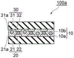
Hereinafter, a circuit connection structure and a method of manufacturing the same, which are one embodiment of the present embodiment, will be described with reference to the drawings. Fig. 1 is a schematic cross-sectional view showing one embodiment of a structure. The circuit connection structure 100a shown in fig. 1 includes a circuit member (first circuit member) 20 and a circuit member (second circuit member) 30 that face each other, and a circuit connection member 10 that connects these members is disposed between the circuit member 20 and the circuit member 30. The circuit connecting member 10 includes a cured product of the adhesive composition of the present embodiment.
The circuit member 20 includes a substrate (first substrate) 21 and a circuit electrode (first circuit electrode) 22 arranged on a main surface 21a of the substrate 21. An insulating layer (not shown) may be disposed on the main surface 21a of the substrate 21 as appropriate.
The circuit member 30 includes a substrate (second substrate) 31 and a circuit electrode (second circuit electrode) 32 disposed on a main surface 31a of the substrate 31. An insulating layer (not shown) may be disposed on the main surface 31a of the substrate 31 as appropriate.
The circuit connecting member 10 includes an insulating material (cured product of a component other than conductive particles) 10a and conductive particles 10 b. The conductive particles 10b are disposed at least between the circuit electrodes 22 and 32 facing each other. In the circuit connection structure 100a, the circuit electrode 22 and the circuit electrode 32 are electrically connected via the conductive particles 10 b.
The circuit members 20 and 30 have single or multiple circuit electrodes (connection terminals). As the circuit members 20 and 30, for example, members having electrodes that require electrical connection may be used. As the circuit member, chip components such as a semiconductor chip (IC chip), a resistor chip, and a capacitor chip; printed circuit boards, semiconductor mounting boards, and the like. Examples of the combination of the circuit members 20 and 30 include a semiconductor chip and a semiconductor mounting board. Examples of the material of the substrate include inorganic substances such as semiconductors, glasses, and ceramics; organic materials such as polyimide, polyethylene terephthalate, polycarbonate, (meth) acrylic resin, and cyclic olefin resin; composites of glass with epoxy, etc. The substrate may also be a plastic substrate.
Fig. 2 is a schematic cross-sectional view showing another embodiment of the structure. The circuit connection structure 100b shown in fig. 2 has the same configuration as the circuit connection structure 100a except that the circuit connection member 10 does not contain the conductive particles 10 b. In the circuit connection structure 100b shown in fig. 2, the circuit electrode 22 and the circuit electrode 32 are in direct contact without conductive particles interposed therebetween, and are electrically connected.
The circuit connection structures 100a and 100b can be manufactured by the following method, for example. First, when the adhesive composition is in a paste form, the adhesive composition is applied and dried, whereby a resin layer containing the adhesive composition is disposed on the circuit member 20. When the adhesive composition is in the form of a film, the resin layer containing the adhesive composition is disposed on the circuit member 20 by attaching the film-shaped adhesive composition to the circuit member 20. Next, the circuit member 30 is placed on the resin layer disposed on the circuit member 20 so that the circuit electrodes 22 are disposed opposite to the circuit electrodes 32. Then, the resin layer containing the adhesive composition is subjected to heat treatment or light irradiation, thereby curing the adhesive composition to obtain a cured product (circuit connecting member 10). From the above, the circuit connection structures 100a and 100b are obtained.
Examples
The present invention will be described in more detail below with reference to examples and comparative examples. However, the present invention is not limited to the following examples.
(Synthesis of polyurethane)
Into a separable flask equipped with a reflux condenser, a thermometer and a stirrer, 1000 parts by mass of polypropylene glycol (anda number average molecular weight Mn of 2000, manufactured by mitsubishi kosha co.ltd., and 4000 parts by mass of methyl ethyl ketone (solvent), and then stirred at 40 ℃ for 30 minutes to prepare a reaction solution. After the temperature of the reaction solution was raised to 70 ℃, 0.0127 parts by mass of dimethyltin laurate (catalyst) was added. Subsequently, a solution prepared by dissolving 125 parts by mass of 4, 4' -diphenylmethane diisocyanate in 125 parts by mass of methyl ethyl ketone was added dropwise to the reaction solution over 1 hour. Then, the stirring was continued at the above temperature until no absorption peak (2270 cm) derived from the isocyanate group could be observed by an infrared spectrophotometer (manufactured by Nippon Kabushiki Kaisha)-1) And obtaining a methyl ethyl ketone solution of polyurethane. Next, the solvent amount was adjusted so that the solid content concentration (concentration of polyurethane) of the solution became 30 mass%. The weight average molecular weight of the obtained polyurethane (urethane resin) was measured by GPC (gel permeation chromatography), and the result was 320000 (standard polystyrene equivalent). The measurement conditions of GPC are shown in table 1.
[ Table 1]

(Synthesis of urethane acrylate)
A2L (liter) four-necked flask equipped with a thermometer, a stirrer, an inert gas inlet and a reflux condenser was charged with 4000 parts by mass of polycarbonate diol (manufactured by Aldrich Co., Ltd., number average molecular weight 2000), 238 parts by mass of 2-hydroxyethyl acrylate, 0.49 part by mass of hydroquinone monomethyl ether and 4.9 parts by mass of a tin catalyst to prepare a reaction mixture. 666 parts by mass of isophorone diisocyanate (IPDI) was uniformly added dropwise to the reaction solution heated to 70 ℃ over 3 hours, and the reaction was carried out. After completion of the dropwise addition, the reaction was continued for 15 hours, and a point of time at which the NCO% (NCO content) was less than or equal to 0.2 mass% was regarded as the end of the reaction, to obtain a urethane acrylate. NCO% was confirmed by a potentiometric automatic titrator (trade name: AT-510, manufactured by Kyoto electronics Co., Ltd.). Analysis by GPC revealed that the weight average molecular weight of the urethane acrylate was 8500 (calculated as standard polystyrene). The analysis by GPC was performed under the same conditions as the analysis of the weight average molecular weight of the polyurethane.
(preparation of conductive particles)
A nickel layer having a thickness of 0.2 μm was formed on the surface of the polystyrene particles. Further, a gold layer having a thickness of 0.04 μm was formed on the outer side of the nickel layer. Thus, conductive particles having an average particle diameter of 4 μm were produced.
(preparation of film-shaped adhesive)
The components shown in tables 2 and 3 were mixed at the mass ratios (solid contents) shown in tables 2 and 3 to obtain mixtures. The conductive particles were dispersed in the mixture at a ratio of 1.5 vol% (basis: total volume of the binder component of the binder composition) to obtain a coating liquid for forming a film-like binder. The coating liquid was coated on a polyethylene terephthalate (PET) film having a thickness of 50 μm using a coating apparatus. The coating film was hot-air dried at 70 ℃ for 10 minutes to form a film-like adhesive having a thickness of 18 μm.
The phenoxy resins shown in tables 2 and 3 were used in the form of a 40 mass% solution prepared by dissolving 40g of PKHC (product name, weight average molecular weight 45000, manufactured by union carbide co., ltd.) in 60g of methyl ethyl ketone. As the polyurethane, the polyurethane synthesized as described above is used. As the radical polymerizable compound a, the urethane acrylate synthesized as described above was used. As the radical polymerizable compound B, isocyanuric acid EO-modified diacrylate (trade name: M-215, manufactured by Toyo chemical Co., Ltd.) was used. As the radically polymerizable compound C (phosphate ester), 2-methacryloyloxyethyl acid phosphate (trade name: LIGHT ESTER P-2M, manufactured by Kyoeisha chemical Co., Ltd.) was used. As the radical polymerizable compound D, 9-bis- [4- (2-acryloyloxyethoxy) phenyl ] fluorene (trade name: A-BPEF, manufactured by shinkamura chemical Co., Ltd.) was used.
As the silane compound (1 st silane compound) having a radical polymerizable functional group (a functional group participating in a curing radical polymerization reaction), the following components were used. 3-methacryloxypropylmethyldimethoxysilane (trade name: KBM-502, manufactured by shin-Etsu chemical Co., Ltd.) was used as silane compound A1, 3-methacryloxypropyltrimethoxysilane (trade name: KBM-503, manufactured by shin-Etsu chemical Co., Ltd.) was used as silane compound A2, and 3-acryloxypropyltrimethoxysilane (trade name: KBM-5103, manufactured by shin-Etsu chemical Co., Ltd.) was used as silane compound A3.
As the silane compound (2 nd silane compound) having a functional group not participating in the curing radical polymerization reaction and not having a radical polymerizable functional group (a functional group participating in the curing radical polymerization reaction), the following components were used. 3-glycidoxypropylmethyldimethoxysilane (trade name: KBM-402, manufactured by shin-Etsu chemical Co., Ltd.) was used as the silane compound B1, 3-glycidoxypropyltrimethoxysilane (trade name: KBM-403, manufactured by shin-Etsu chemical Co., Ltd.) was used as the silane compound B2, and methyltrimethoxysilane (trade name: KBM-13, manufactured by shin-Etsu chemical Co., Ltd.) was used as the silane compound B3.
As the radical polymerization initiator, dilauroyl peroxide (peroxide A1, trade name: PEROYL L, manufactured by Nichikoku K.K., 1-minute half-life temperature: 116.4 ℃ C.), tert-butyl peroxypivalate (peroxide A2, trade name: PERBUTYL PV, manufactured by Nichikoku K.K., 1-minute half-life temperature: 110.3 ℃ C.), and 1,1,3, 3-tetramethylbutyl peroxy2-ethylhexanoate (peroxide B, trade name: PEROCTAO, manufactured by Nichikoku K.K., 1-minute half-life temperature: 124.3 ℃ C.) were used.
10g of silica particles (trade name: R104, manufactured by AEROSIL corporation, Japan) as inorganic particles were dispersed in a mixed solvent of 45g of toluene and 45g of ethyl acetate to prepare a 10 mass% dispersion, which was then mixed with the coating liquid.
(preparation of connector)
A flexible circuit board (FPC) was bonded to SiN using the film-like adhesives shown in tables 2 and 3xSubstrate (thickness 0.7mm) connection, the flexible circuit substrate has 2200 line widths 75 μm and a pitch150 μm (gap 75 μm) and 18 μm thick copper circuitry, SiNxThe substrate has a glass substrate and 0.2 μm thick silicon nitride (SiN) formed on the glass substratex) A thin layer. The connection was carried out by heating and pressing at 130 ℃ and 3MPa for 5 seconds or at 170 ℃ and 3MPa for 5 seconds using a thermocompression bonding apparatus (heating system: constant temperature type, manufactured by Toray engineering Co., Ltd.). Thus, FPC and SiN were produced by curing the film-like adhesivexThe substrates were connected to each other with a width of 1.5 mm. The pressure contact area was set to 0.495cm2And calculating the pressurization pressure.
(evaluation of peeling)
The appearance of the connection immediately after the production of the interconnector and the appearance of the connection after the interconnector was left in a constant temperature and humidity chamber at 85 ℃ and 85% RH for 250 hours (after the high temperature and high humidity test) were observed with an optical microscope. In the measurement gap portion in SiNxThe area where peeling occurred at the interface between the substrate and the cured product (peeled area) was evaluated for the presence or absence of peeling. The case where the ratio of the peeled area to the entire gap was more than 30% was evaluated as "B" (peeling), and the case where the ratio of the peeled area was 30% or less was evaluated as "a" (no peeling). The evaluation results are shown in tables 2 and 3. In addition, regarding the appearance of the connection body immediately after the production thereof, the peeling was not generated in all the examples and comparative examples.
(evaluation of storage stability (Life characteristics))
The film-like adhesive was treated in a thermostatic bath at 40 ℃ for 1 day. Using this film-like adhesive, a connected body was produced by the same method as described above, and then subjected to a high temperature and high humidity test. The evaluation results are shown in tables 2 and 3.
[ Table 2]

[ Table 3]

As confirmed from tables 2 and 3: the film-like adhesives of the examples can be bonded at a low temperature for a short time (particularly at 130 ℃ C. for 5 seconds) as compared with the comparative examples. In addition, it was confirmed that: the film-like adhesive of the examples can maintain the adhesion force to the surface of the substrate (inorganic substrate) well even after the high-temperature and high-humidity treatment, and is excellent in storage stability, as compared with the comparative examples.
Description of the symbols
10: a circuit connection member; 10 a: an insulating material; 10 b: conductive particles; 20: a first circuit member; 21: a first substrate; 21 a: a main face; 22: a first circuit electrode; 30: a second circuit member; 31: a second substrate; 31 a: a main face; 32: a second circuit electrode; 100a, 100 b: a circuit connection structure.
Claims (6)
1. An adhesive composition comprising:
a1 st silane compound having a radical polymerizable functional group;
a2 nd silane compound reacted with the 1 st silane compound;
a radical polymerizable compound, excluding a compound corresponding to the 1 st silane compound;
a peroxide having a1 minute half-life temperature of less than or equal to 120 ℃; and
the conductive particles are formed of a conductive material,
the 2 nd silane compound has no radical polymerizable functional group,
the content of the 1 st silane compound is 0.5 to 20% by mass based on the total mass of the adhesive component of the adhesive composition, that is, the solid component excluding the conductive particles in the adhesive composition.
2. The adhesive composition according to claim 1, wherein the functional group of the 1 st silane compound comprises at least one selected from the group consisting of a (meth) acryloyl group and a vinyl group.
3. The adhesive composition according to claim 1 or 2, wherein the 2 nd silane compound has an epoxy group.
4. The adhesive composition according to claim 1 or 2, which is used for circuit connection.
5. A structure comprising the adhesive composition according to any one of claims 1 to 4 or a cured product thereof.
6. A structure body, comprising:
a first circuit member having a first circuit electrode,
A second circuit member having a second circuit electrode, and
a circuit connecting member disposed between the first circuit member and the second circuit member,
the first circuit electrode and the second circuit electrode are electrically connected,
the circuit connecting member comprises the adhesive composition according to any one of claims 1 to 4 or a cured product thereof.
Applications Claiming Priority (3)
| Application Number | Priority Date | Filing Date | Title |
|---|---|---|---|
| JP2015-216516 | 2015-11-04 | ||
| JP2015216516 | 2015-11-04 | ||
| PCT/JP2016/082645 WO2017078087A1 (en) | 2015-11-04 | 2016-11-02 | Adhesive composition and structure |
Publications (2)
| Publication Number | Publication Date |
|---|---|
| CN108350320A CN108350320A (en) | 2018-07-31 |
| CN108350320B true CN108350320B (en) | 2021-11-26 |
Family
ID=58662435
Family Applications (1)
| Application Number | Title | Priority Date | Filing Date |
|---|---|---|---|
| CN201680062847.XA Active CN108350320B (en) | 2015-11-04 | 2016-11-02 | Adhesive composition and structure |
Country Status (5)
| Country | Link |
|---|---|
| JP (2) | JP6915544B2 (en) |
| KR (1) | KR102608218B1 (en) |
| CN (1) | CN108350320B (en) |
| TW (1) | TWI786036B (en) |
| WO (1) | WO2017078087A1 (en) |
Families Citing this family (1)
| Publication number | Priority date | Publication date | Assignee | Title |
|---|---|---|---|---|
| TWI671921B (en) * | 2018-09-14 | 2019-09-11 | 頎邦科技股份有限公司 | Chip package and chip |
Citations (5)
| Publication number | Priority date | Publication date | Assignee | Title |
|---|---|---|---|---|
| CN101675715A (en) * | 2007-05-09 | 2010-03-17 | 日立化成工业株式会社 | Film-like circuit connecting material and connection structure for circuit member |
| CN102942881A (en) * | 2006-05-09 | 2013-02-27 | 日立化成工业株式会社 | Adhesive sheet, and connecting structure for circuit member and semiconductor device which use the adhesive sheet |
| CN103360956A (en) * | 2013-06-18 | 2013-10-23 | 明基材料有限公司 | Sticking agent for electrical property conduction between electronic components |
| CN103764776A (en) * | 2011-09-06 | 2014-04-30 | 日立化成株式会社 | Adhesive composition and connection body |
| CN104559902A (en) * | 2013-10-09 | 2015-04-29 | 日立化成株式会社 | Circuit connecting material, connection structure of circuit members, and method for manufacturing connection structure of circuit member |
Family Cites Families (16)
| Publication number | Priority date | Publication date | Assignee | Title |
|---|---|---|---|---|
| JP2002285103A (en) * | 2001-03-26 | 2002-10-03 | Sumitomo Bakelite Co Ltd | Anisotropic electroconductive adhesive |
| JP4004333B2 (en) * | 2001-06-05 | 2007-11-07 | 松下電器産業株式会社 | Semiconductor module |
| JP2004067908A (en) * | 2002-08-07 | 2004-03-04 | Sumitomo Bakelite Co Ltd | Anisotropically electroconductive adhesive |
| JP4146747B2 (en) * | 2003-03-26 | 2008-09-10 | 積水化学工業株式会社 | Curable composition |
| JP2006022231A (en) * | 2004-07-08 | 2006-01-26 | Sumitomo Bakelite Co Ltd | Anisotropically conductive adhesive and anisotropically conductive adhesive film |
| KR20100080628A (en) | 2007-11-12 | 2010-07-09 | 히다치 가세고교 가부시끼가이샤 | Circuit connecting material and structure for connecting circuit member |
| KR101343864B1 (en) * | 2009-03-23 | 2013-12-20 | 세메다인 가부시키 가이샤 | Curable composition |
| JP2011199097A (en) * | 2010-03-23 | 2011-10-06 | Sumitomo Bakelite Co Ltd | Method of manufacturing semiconductor device |
| JP2012072305A (en) * | 2010-09-29 | 2012-04-12 | Hitachi Chemical Co Ltd | Resin paste composition |
| JP5909911B2 (en) * | 2011-07-29 | 2016-04-27 | 住友ベークライト株式会社 | Liquid resin composition and semiconductor device |
| JP5934528B2 (en) | 2012-03-12 | 2016-06-15 | デクセリアルズ株式会社 | CIRCUIT CONNECTION MATERIAL, AND METHOD FOR MANUFACTURING MOUNTING BODY USING THE SAME |
| JP6250265B2 (en) * | 2012-03-16 | 2017-12-20 | リンテック株式会社 | Adhesive composition, adhesive sheet, and method for manufacturing semiconductor device |
| WO2013161713A1 (en) * | 2012-04-25 | 2013-10-31 | 日立化成株式会社 | Circuit connection material, circuit connection structure, adhesive film, and wound body |
| JP2013253151A (en) * | 2012-06-06 | 2013-12-19 | Hitachi Chemical Co Ltd | Adhesive film for circuit connection, and connection structure of circuit member and manufacturing method thereof |
| CN103131336B (en) * | 2013-03-22 | 2015-06-10 | 苏州度辰新材料有限公司 | Preparation method of silane crosslinked ethylene-vinyl acetate copolymer adhesive film |
| JP6437323B2 (en) * | 2014-02-14 | 2018-12-12 | デクセリアルズ株式会社 | Manufacturing method of connection structure and circuit connection material |
-
2016
- 2016-11-02 WO PCT/JP2016/082645 patent/WO2017078087A1/en active Application Filing
- 2016-11-02 JP JP2017548820A patent/JP6915544B2/en active Active
- 2016-11-02 KR KR1020187014964A patent/KR102608218B1/en active IP Right Grant
- 2016-11-02 CN CN201680062847.XA patent/CN108350320B/en active Active
- 2016-11-03 TW TW105135632A patent/TWI786036B/en active
-
2021
- 2021-07-01 JP JP2021110078A patent/JP7124936B2/en active Active
Patent Citations (5)
| Publication number | Priority date | Publication date | Assignee | Title |
|---|---|---|---|---|
| CN102942881A (en) * | 2006-05-09 | 2013-02-27 | 日立化成工业株式会社 | Adhesive sheet, and connecting structure for circuit member and semiconductor device which use the adhesive sheet |
| CN101675715A (en) * | 2007-05-09 | 2010-03-17 | 日立化成工业株式会社 | Film-like circuit connecting material and connection structure for circuit member |
| CN103764776A (en) * | 2011-09-06 | 2014-04-30 | 日立化成株式会社 | Adhesive composition and connection body |
| CN103360956A (en) * | 2013-06-18 | 2013-10-23 | 明基材料有限公司 | Sticking agent for electrical property conduction between electronic components |
| CN104559902A (en) * | 2013-10-09 | 2015-04-29 | 日立化成株式会社 | Circuit connecting material, connection structure of circuit members, and method for manufacturing connection structure of circuit member |
Also Published As
| Publication number | Publication date |
|---|---|
| WO2017078087A1 (en) | 2017-05-11 |
| TWI786036B (en) | 2022-12-11 |
| JP6915544B2 (en) | 2021-08-04 |
| KR20180079370A (en) | 2018-07-10 |
| TW201724924A (en) | 2017-07-01 |
| JP2021165397A (en) | 2021-10-14 |
| KR102608218B1 (en) | 2023-11-30 |
| JP7124936B2 (en) | 2022-08-24 |
| CN108350320A (en) | 2018-07-31 |
| JPWO2017078087A1 (en) | 2018-09-06 |
Similar Documents
| Publication | Publication Date | Title |
|---|---|---|
| KR101970376B1 (en) | Adhesive composition and connection body | |
| JP6307966B2 (en) | Adhesive composition, anisotropic conductive adhesive composition, circuit connection material and connector | |
| KR20210134875A (en) | Adhesive composition and connected structure | |
| WO2017090659A1 (en) | Adhesive composition for circuit connection, and structure | |
| JP7172991B2 (en) | Adhesive composition and structure | |
| JP7124936B2 (en) | Adhesive composition and structure | |
| CN111995975B (en) | Adhesive composition and structure | |
| TWI811185B (en) | Adhesive composition and structure | |
| KR102467385B1 (en) | Connection structure, circuit connection member and adhesive composition | |
| CN107922817B (en) | Adhesive composition, anisotropic conductive adhesive composition, circuit connecting material, and connected body |
Legal Events
| Date | Code | Title | Description |
|---|---|---|---|
| PB01 | Publication | ||
| PB01 | Publication | ||
| SE01 | Entry into force of request for substantive examination | ||
| SE01 | Entry into force of request for substantive examination | ||
| CB02 | Change of applicant information | ||
| CB02 | Change of applicant information |
Address after: Tokyo, Japan Applicant after: Showa electrical materials Co.,Ltd. Address before: Tokyo, Japan Applicant before: HITACHI CHEMICAL Co.,Ltd. |
|
| GR01 | Patent grant | ||
| GR01 | Patent grant | ||
| CP01 | Change in the name or title of a patent holder | ||
| CP01 | Change in the name or title of a patent holder |
Address after: Tokyo, Japan Patentee after: Lishennoco Co.,Ltd. Address before: Tokyo, Japan Patentee before: Showa electrical materials Co.,Ltd. |