CN108231904B - Thin film transistor, driving method thereof, display device and transistor circuit - Google Patents
Thin film transistor, driving method thereof, display device and transistor circuit Download PDFInfo
- Publication number
- CN108231904B CN108231904B CN201711190146.7A CN201711190146A CN108231904B CN 108231904 B CN108231904 B CN 108231904B CN 201711190146 A CN201711190146 A CN 201711190146A CN 108231904 B CN108231904 B CN 108231904B
- Authority
- CN
- China
- Prior art keywords
- thin film
- channel
- electrode
- film transistor
- source electrode
- Prior art date
- Legal status (The legal status is an assumption and is not a legal conclusion. Google has not performed a legal analysis and makes no representation as to the accuracy of the status listed.)
- Active
Links
- 239000010409 thin film Substances 0.000 title claims abstract description 44
- 238000000034 method Methods 0.000 title claims abstract description 8
- 239000010408 film Substances 0.000 claims abstract description 84
- 239000004065 semiconductor Substances 0.000 claims abstract description 39
- 238000005530 etching Methods 0.000 claims description 20
- 239000003990 capacitor Substances 0.000 claims description 17
- 238000002161 passivation Methods 0.000 claims description 15
- 239000010410 layer Substances 0.000 description 54
- 238000010586 diagram Methods 0.000 description 18
- 239000000758 substrate Substances 0.000 description 14
- 230000000694 effects Effects 0.000 description 10
- 239000011229 interlayer Substances 0.000 description 5
- 229910021417 amorphous silicon Inorganic materials 0.000 description 4
- QVGXLLKOCUKJST-UHFFFAOYSA-N atomic oxygen Chemical compound [O] QVGXLLKOCUKJST-UHFFFAOYSA-N 0.000 description 4
- 230000015556 catabolic process Effects 0.000 description 4
- 150000001875 compounds Chemical class 0.000 description 4
- 230000007423 decrease Effects 0.000 description 4
- 238000006731 degradation reaction Methods 0.000 description 4
- 229910052738 indium Inorganic materials 0.000 description 4
- APFVFJFRJDLVQX-UHFFFAOYSA-N indium atom Chemical compound [In] APFVFJFRJDLVQX-UHFFFAOYSA-N 0.000 description 4
- 239000000463 material Substances 0.000 description 4
- 229910052760 oxygen Inorganic materials 0.000 description 4
- 239000001301 oxygen Substances 0.000 description 4
- 239000000126 substance Substances 0.000 description 4
- 230000002349 favourable effect Effects 0.000 description 3
- 238000010030 laminating Methods 0.000 description 3
- 229910052751 metal Inorganic materials 0.000 description 3
- 239000002184 metal Substances 0.000 description 3
- 238000004804 winding Methods 0.000 description 3
- 229910000838 Al alloy Inorganic materials 0.000 description 2
- 229910000881 Cu alloy Inorganic materials 0.000 description 2
- GYHNNYVSQQEPJS-UHFFFAOYSA-N Gallium Chemical compound [Ga] GYHNNYVSQQEPJS-UHFFFAOYSA-N 0.000 description 2
- ZOKXTWBITQBERF-UHFFFAOYSA-N Molybdenum Chemical compound [Mo] ZOKXTWBITQBERF-UHFFFAOYSA-N 0.000 description 2
- 229910052581 Si3N4 Inorganic materials 0.000 description 2
- VYPSYNLAJGMNEJ-UHFFFAOYSA-N Silicium dioxide Chemical compound O=[Si]=O VYPSYNLAJGMNEJ-UHFFFAOYSA-N 0.000 description 2
- 229910052782 aluminium Inorganic materials 0.000 description 2
- XAGFODPZIPBFFR-UHFFFAOYSA-N aluminium Chemical compound [Al] XAGFODPZIPBFFR-UHFFFAOYSA-N 0.000 description 2
- 239000011651 chromium Substances 0.000 description 2
- 239000010949 copper Substances 0.000 description 2
- 229910052733 gallium Inorganic materials 0.000 description 2
- 239000011521 glass Substances 0.000 description 2
- 239000004973 liquid crystal related substance Substances 0.000 description 2
- 230000007774 longterm Effects 0.000 description 2
- 150000002739 metals Chemical class 0.000 description 2
- 238000012986 modification Methods 0.000 description 2
- 230000004048 modification Effects 0.000 description 2
- 229910052750 molybdenum Inorganic materials 0.000 description 2
- 239000011733 molybdenum Substances 0.000 description 2
- 239000010955 niobium Substances 0.000 description 2
- HQVNEWCFYHHQES-UHFFFAOYSA-N silicon nitride Chemical compound N12[Si]34N5[Si]62N3[Si]51N64 HQVNEWCFYHHQES-UHFFFAOYSA-N 0.000 description 2
- 229910052814 silicon oxide Inorganic materials 0.000 description 2
- WFKWXMTUELFFGS-UHFFFAOYSA-N tungsten Chemical compound [W] WFKWXMTUELFFGS-UHFFFAOYSA-N 0.000 description 2
- 229910052721 tungsten Inorganic materials 0.000 description 2
- 239000010937 tungsten Substances 0.000 description 2
- 229910001316 Ag alloy Inorganic materials 0.000 description 1
- VYZAMTAEIAYCRO-UHFFFAOYSA-N Chromium Chemical compound [Cr] VYZAMTAEIAYCRO-UHFFFAOYSA-N 0.000 description 1
- RYGMFSIKBFXOCR-UHFFFAOYSA-N Copper Chemical compound [Cu] RYGMFSIKBFXOCR-UHFFFAOYSA-N 0.000 description 1
- 102100040862 Dual specificity protein kinase CLK1 Human genes 0.000 description 1
- 101000749294 Homo sapiens Dual specificity protein kinase CLK1 Proteins 0.000 description 1
- 229910001182 Mo alloy Inorganic materials 0.000 description 1
- XUIMIQQOPSSXEZ-UHFFFAOYSA-N Silicon Chemical compound [Si] XUIMIQQOPSSXEZ-UHFFFAOYSA-N 0.000 description 1
- BQCADISMDOOEFD-UHFFFAOYSA-N Silver Chemical compound [Ag] BQCADISMDOOEFD-UHFFFAOYSA-N 0.000 description 1
- 229910001069 Ti alloy Inorganic materials 0.000 description 1
- RTAQQCXQSZGOHL-UHFFFAOYSA-N Titanium Chemical compound [Ti] RTAQQCXQSZGOHL-UHFFFAOYSA-N 0.000 description 1
- HCHKCACWOHOZIP-UHFFFAOYSA-N Zinc Chemical compound [Zn] HCHKCACWOHOZIP-UHFFFAOYSA-N 0.000 description 1
- 229910045601 alloy Inorganic materials 0.000 description 1
- 239000000956 alloy Substances 0.000 description 1
- 229910052804 chromium Inorganic materials 0.000 description 1
- 239000000470 constituent Substances 0.000 description 1
- 229910052802 copper Inorganic materials 0.000 description 1
- 230000009977 dual effect Effects 0.000 description 1
- 230000012447 hatching Effects 0.000 description 1
- 238000003475 lamination Methods 0.000 description 1
- 239000011159 matrix material Substances 0.000 description 1
- 238000005259 measurement Methods 0.000 description 1
- 239000000178 monomer Substances 0.000 description 1
- 229910052758 niobium Inorganic materials 0.000 description 1
- GUCVJGMIXFAOAE-UHFFFAOYSA-N niobium atom Chemical compound [Nb] GUCVJGMIXFAOAE-UHFFFAOYSA-N 0.000 description 1
- TWNQGVIAIRXVLR-UHFFFAOYSA-N oxo(oxoalumanyloxy)alumane Chemical compound O=[Al]O[Al]=O TWNQGVIAIRXVLR-UHFFFAOYSA-N 0.000 description 1
- BPUBBGLMJRNUCC-UHFFFAOYSA-N oxygen(2-);tantalum(5+) Chemical compound [O-2].[O-2].[O-2].[O-2].[O-2].[Ta+5].[Ta+5] BPUBBGLMJRNUCC-UHFFFAOYSA-N 0.000 description 1
- 230000002093 peripheral effect Effects 0.000 description 1
- 229910052710 silicon Inorganic materials 0.000 description 1
- 239000010703 silicon Substances 0.000 description 1
- LIVNPJMFVYWSIS-UHFFFAOYSA-N silicon monoxide Chemical compound [Si-]#[O+] LIVNPJMFVYWSIS-UHFFFAOYSA-N 0.000 description 1
- 229910052709 silver Inorganic materials 0.000 description 1
- 239000004332 silver Substances 0.000 description 1
- 239000002356 single layer Substances 0.000 description 1
- 230000000087 stabilizing effect Effects 0.000 description 1
- 229910001936 tantalum oxide Inorganic materials 0.000 description 1
- JBQYATWDVHIOAR-UHFFFAOYSA-N tellanylidenegermanium Chemical compound [Te]=[Ge] JBQYATWDVHIOAR-UHFFFAOYSA-N 0.000 description 1
- 239000010936 titanium Substances 0.000 description 1
- 229910052719 titanium Inorganic materials 0.000 description 1
- 229910052725 zinc Inorganic materials 0.000 description 1
- 239000011701 zinc Substances 0.000 description 1
Images


Classifications
-
- H—ELECTRICITY
- H01—ELECTRIC ELEMENTS
- H01L—SEMICONDUCTOR DEVICES NOT COVERED BY CLASS H10
- H01L29/00—Semiconductor devices adapted for rectifying, amplifying, oscillating or switching, or capacitors or resistors with at least one potential-jump barrier or surface barrier, e.g. PN junction depletion layer or carrier concentration layer; Details of semiconductor bodies or of electrodes thereof ; Multistep manufacturing processes therefor
- H01L29/66—Types of semiconductor device ; Multistep manufacturing processes therefor
- H01L29/68—Types of semiconductor device ; Multistep manufacturing processes therefor controllable by only the electric current supplied, or only the electric potential applied, to an electrode which does not carry the current to be rectified, amplified or switched
- H01L29/76—Unipolar devices, e.g. field effect transistors
- H01L29/772—Field effect transistors
- H01L29/78—Field effect transistors with field effect produced by an insulated gate
- H01L29/786—Thin film transistors, i.e. transistors with a channel being at least partly a thin film
- H01L29/7869—Thin film transistors, i.e. transistors with a channel being at least partly a thin film having a semiconductor body comprising an oxide semiconductor material, e.g. zinc oxide, copper aluminium oxide, cadmium stannate
- H01L29/78693—Thin film transistors, i.e. transistors with a channel being at least partly a thin film having a semiconductor body comprising an oxide semiconductor material, e.g. zinc oxide, copper aluminium oxide, cadmium stannate the semiconducting oxide being amorphous
-
- H—ELECTRICITY
- H01—ELECTRIC ELEMENTS
- H01L—SEMICONDUCTOR DEVICES NOT COVERED BY CLASS H10
- H01L27/00—Devices consisting of a plurality of semiconductor or other solid-state components formed in or on a common substrate
- H01L27/02—Devices consisting of a plurality of semiconductor or other solid-state components formed in or on a common substrate including semiconductor components specially adapted for rectifying, oscillating, amplifying or switching and having at least one potential-jump barrier or surface barrier; including integrated passive circuit elements with at least one potential-jump barrier or surface barrier
- H01L27/12—Devices consisting of a plurality of semiconductor or other solid-state components formed in or on a common substrate including semiconductor components specially adapted for rectifying, oscillating, amplifying or switching and having at least one potential-jump barrier or surface barrier; including integrated passive circuit elements with at least one potential-jump barrier or surface barrier the substrate being other than a semiconductor body, e.g. an insulating body
- H01L27/1214—Devices consisting of a plurality of semiconductor or other solid-state components formed in or on a common substrate including semiconductor components specially adapted for rectifying, oscillating, amplifying or switching and having at least one potential-jump barrier or surface barrier; including integrated passive circuit elements with at least one potential-jump barrier or surface barrier the substrate being other than a semiconductor body, e.g. an insulating body comprising a plurality of TFTs formed on a non-semiconducting substrate, e.g. driving circuits for AMLCDs
- H01L27/1222—Devices consisting of a plurality of semiconductor or other solid-state components formed in or on a common substrate including semiconductor components specially adapted for rectifying, oscillating, amplifying or switching and having at least one potential-jump barrier or surface barrier; including integrated passive circuit elements with at least one potential-jump barrier or surface barrier the substrate being other than a semiconductor body, e.g. an insulating body comprising a plurality of TFTs formed on a non-semiconducting substrate, e.g. driving circuits for AMLCDs with a particular composition, shape or crystalline structure of the active layer
- H01L27/1225—Devices consisting of a plurality of semiconductor or other solid-state components formed in or on a common substrate including semiconductor components specially adapted for rectifying, oscillating, amplifying or switching and having at least one potential-jump barrier or surface barrier; including integrated passive circuit elements with at least one potential-jump barrier or surface barrier the substrate being other than a semiconductor body, e.g. an insulating body comprising a plurality of TFTs formed on a non-semiconducting substrate, e.g. driving circuits for AMLCDs with a particular composition, shape or crystalline structure of the active layer with semiconductor materials not belonging to the group IV of the periodic table, e.g. InGaZnO
-
- G—PHYSICS
- G09—EDUCATION; CRYPTOGRAPHY; DISPLAY; ADVERTISING; SEALS
- G09G—ARRANGEMENTS OR CIRCUITS FOR CONTROL OF INDICATING DEVICES USING STATIC MEANS TO PRESENT VARIABLE INFORMATION
- G09G3/00—Control arrangements or circuits, of interest only in connection with visual indicators other than cathode-ray tubes
- G09G3/20—Control arrangements or circuits, of interest only in connection with visual indicators other than cathode-ray tubes for presentation of an assembly of a number of characters, e.g. a page, by composing the assembly by combination of individual elements arranged in a matrix no fixed position being assigned to or needed to be assigned to the individual characters or partial characters
- G09G3/22—Control arrangements or circuits, of interest only in connection with visual indicators other than cathode-ray tubes for presentation of an assembly of a number of characters, e.g. a page, by composing the assembly by combination of individual elements arranged in a matrix no fixed position being assigned to or needed to be assigned to the individual characters or partial characters using controlled light sources
- G09G3/30—Control arrangements or circuits, of interest only in connection with visual indicators other than cathode-ray tubes for presentation of an assembly of a number of characters, e.g. a page, by composing the assembly by combination of individual elements arranged in a matrix no fixed position being assigned to or needed to be assigned to the individual characters or partial characters using controlled light sources using electroluminescent panels
- G09G3/32—Control arrangements or circuits, of interest only in connection with visual indicators other than cathode-ray tubes for presentation of an assembly of a number of characters, e.g. a page, by composing the assembly by combination of individual elements arranged in a matrix no fixed position being assigned to or needed to be assigned to the individual characters or partial characters using controlled light sources using electroluminescent panels semiconductive, e.g. using light-emitting diodes [LED]
- G09G3/3208—Control arrangements or circuits, of interest only in connection with visual indicators other than cathode-ray tubes for presentation of an assembly of a number of characters, e.g. a page, by composing the assembly by combination of individual elements arranged in a matrix no fixed position being assigned to or needed to be assigned to the individual characters or partial characters using controlled light sources using electroluminescent panels semiconductive, e.g. using light-emitting diodes [LED] organic, e.g. using organic light-emitting diodes [OLED]
- G09G3/3225—Control arrangements or circuits, of interest only in connection with visual indicators other than cathode-ray tubes for presentation of an assembly of a number of characters, e.g. a page, by composing the assembly by combination of individual elements arranged in a matrix no fixed position being assigned to or needed to be assigned to the individual characters or partial characters using controlled light sources using electroluminescent panels semiconductive, e.g. using light-emitting diodes [LED] organic, e.g. using organic light-emitting diodes [OLED] using an active matrix
- G09G3/3233—Control arrangements or circuits, of interest only in connection with visual indicators other than cathode-ray tubes for presentation of an assembly of a number of characters, e.g. a page, by composing the assembly by combination of individual elements arranged in a matrix no fixed position being assigned to or needed to be assigned to the individual characters or partial characters using controlled light sources using electroluminescent panels semiconductive, e.g. using light-emitting diodes [LED] organic, e.g. using organic light-emitting diodes [OLED] using an active matrix with pixel circuitry controlling the current through the light-emitting element
-
- G—PHYSICS
- G09—EDUCATION; CRYPTOGRAPHY; DISPLAY; ADVERTISING; SEALS
- G09G—ARRANGEMENTS OR CIRCUITS FOR CONTROL OF INDICATING DEVICES USING STATIC MEANS TO PRESENT VARIABLE INFORMATION
- G09G3/00—Control arrangements or circuits, of interest only in connection with visual indicators other than cathode-ray tubes
- G09G3/20—Control arrangements or circuits, of interest only in connection with visual indicators other than cathode-ray tubes for presentation of an assembly of a number of characters, e.g. a page, by composing the assembly by combination of individual elements arranged in a matrix no fixed position being assigned to or needed to be assigned to the individual characters or partial characters
- G09G3/22—Control arrangements or circuits, of interest only in connection with visual indicators other than cathode-ray tubes for presentation of an assembly of a number of characters, e.g. a page, by composing the assembly by combination of individual elements arranged in a matrix no fixed position being assigned to or needed to be assigned to the individual characters or partial characters using controlled light sources
- G09G3/30—Control arrangements or circuits, of interest only in connection with visual indicators other than cathode-ray tubes for presentation of an assembly of a number of characters, e.g. a page, by composing the assembly by combination of individual elements arranged in a matrix no fixed position being assigned to or needed to be assigned to the individual characters or partial characters using controlled light sources using electroluminescent panels
- G09G3/32—Control arrangements or circuits, of interest only in connection with visual indicators other than cathode-ray tubes for presentation of an assembly of a number of characters, e.g. a page, by composing the assembly by combination of individual elements arranged in a matrix no fixed position being assigned to or needed to be assigned to the individual characters or partial characters using controlled light sources using electroluminescent panels semiconductive, e.g. using light-emitting diodes [LED]
- G09G3/3208—Control arrangements or circuits, of interest only in connection with visual indicators other than cathode-ray tubes for presentation of an assembly of a number of characters, e.g. a page, by composing the assembly by combination of individual elements arranged in a matrix no fixed position being assigned to or needed to be assigned to the individual characters or partial characters using controlled light sources using electroluminescent panels semiconductive, e.g. using light-emitting diodes [LED] organic, e.g. using organic light-emitting diodes [OLED]
- G09G3/3266—Details of drivers for scan electrodes
-
- G—PHYSICS
- G09—EDUCATION; CRYPTOGRAPHY; DISPLAY; ADVERTISING; SEALS
- G09G—ARRANGEMENTS OR CIRCUITS FOR CONTROL OF INDICATING DEVICES USING STATIC MEANS TO PRESENT VARIABLE INFORMATION
- G09G3/00—Control arrangements or circuits, of interest only in connection with visual indicators other than cathode-ray tubes
- G09G3/20—Control arrangements or circuits, of interest only in connection with visual indicators other than cathode-ray tubes for presentation of an assembly of a number of characters, e.g. a page, by composing the assembly by combination of individual elements arranged in a matrix no fixed position being assigned to or needed to be assigned to the individual characters or partial characters
- G09G3/34—Control arrangements or circuits, of interest only in connection with visual indicators other than cathode-ray tubes for presentation of an assembly of a number of characters, e.g. a page, by composing the assembly by combination of individual elements arranged in a matrix no fixed position being assigned to or needed to be assigned to the individual characters or partial characters by control of light from an independent source
- G09G3/36—Control arrangements or circuits, of interest only in connection with visual indicators other than cathode-ray tubes for presentation of an assembly of a number of characters, e.g. a page, by composing the assembly by combination of individual elements arranged in a matrix no fixed position being assigned to or needed to be assigned to the individual characters or partial characters by control of light from an independent source using liquid crystals
- G09G3/3611—Control of matrices with row and column drivers
- G09G3/3648—Control of matrices with row and column drivers using an active matrix
- G09G3/3655—Details of drivers for counter electrodes, e.g. common electrodes for pixel capacitors or supplementary storage capacitors
-
- G—PHYSICS
- G09—EDUCATION; CRYPTOGRAPHY; DISPLAY; ADVERTISING; SEALS
- G09G—ARRANGEMENTS OR CIRCUITS FOR CONTROL OF INDICATING DEVICES USING STATIC MEANS TO PRESENT VARIABLE INFORMATION
- G09G3/00—Control arrangements or circuits, of interest only in connection with visual indicators other than cathode-ray tubes
- G09G3/20—Control arrangements or circuits, of interest only in connection with visual indicators other than cathode-ray tubes for presentation of an assembly of a number of characters, e.g. a page, by composing the assembly by combination of individual elements arranged in a matrix no fixed position being assigned to or needed to be assigned to the individual characters or partial characters
- G09G3/34—Control arrangements or circuits, of interest only in connection with visual indicators other than cathode-ray tubes for presentation of an assembly of a number of characters, e.g. a page, by composing the assembly by combination of individual elements arranged in a matrix no fixed position being assigned to or needed to be assigned to the individual characters or partial characters by control of light from an independent source
- G09G3/36—Control arrangements or circuits, of interest only in connection with visual indicators other than cathode-ray tubes for presentation of an assembly of a number of characters, e.g. a page, by composing the assembly by combination of individual elements arranged in a matrix no fixed position being assigned to or needed to be assigned to the individual characters or partial characters by control of light from an independent source using liquid crystals
- G09G3/3611—Control of matrices with row and column drivers
- G09G3/3674—Details of drivers for scan electrodes
- G09G3/3677—Details of drivers for scan electrodes suitable for active matrices only
-
- H—ELECTRICITY
- H01—ELECTRIC ELEMENTS
- H01L—SEMICONDUCTOR DEVICES NOT COVERED BY CLASS H10
- H01L27/00—Devices consisting of a plurality of semiconductor or other solid-state components formed in or on a common substrate
- H01L27/02—Devices consisting of a plurality of semiconductor or other solid-state components formed in or on a common substrate including semiconductor components specially adapted for rectifying, oscillating, amplifying or switching and having at least one potential-jump barrier or surface barrier; including integrated passive circuit elements with at least one potential-jump barrier or surface barrier
- H01L27/12—Devices consisting of a plurality of semiconductor or other solid-state components formed in or on a common substrate including semiconductor components specially adapted for rectifying, oscillating, amplifying or switching and having at least one potential-jump barrier or surface barrier; including integrated passive circuit elements with at least one potential-jump barrier or surface barrier the substrate being other than a semiconductor body, e.g. an insulating body
-
- H—ELECTRICITY
- H01—ELECTRIC ELEMENTS
- H01L—SEMICONDUCTOR DEVICES NOT COVERED BY CLASS H10
- H01L29/00—Semiconductor devices adapted for rectifying, amplifying, oscillating or switching, or capacitors or resistors with at least one potential-jump barrier or surface barrier, e.g. PN junction depletion layer or carrier concentration layer; Details of semiconductor bodies or of electrodes thereof ; Multistep manufacturing processes therefor
- H01L29/02—Semiconductor bodies ; Multistep manufacturing processes therefor
- H01L29/06—Semiconductor bodies ; Multistep manufacturing processes therefor characterised by their shape; characterised by the shapes, relative sizes, or dispositions of the semiconductor regions ; characterised by the concentration or distribution of impurities within semiconductor regions
- H01L29/10—Semiconductor bodies ; Multistep manufacturing processes therefor characterised by their shape; characterised by the shapes, relative sizes, or dispositions of the semiconductor regions ; characterised by the concentration or distribution of impurities within semiconductor regions with semiconductor regions connected to an electrode not carrying current to be rectified, amplified or switched and such electrode being part of a semiconductor device which comprises three or more electrodes
- H01L29/1025—Channel region of field-effect devices
- H01L29/1029—Channel region of field-effect devices of field-effect transistors
- H01L29/1033—Channel region of field-effect devices of field-effect transistors with insulated gate, e.g. characterised by the length, the width, the geometric contour or the doping structure
-
- H—ELECTRICITY
- H01—ELECTRIC ELEMENTS
- H01L—SEMICONDUCTOR DEVICES NOT COVERED BY CLASS H10
- H01L29/00—Semiconductor devices adapted for rectifying, amplifying, oscillating or switching, or capacitors or resistors with at least one potential-jump barrier or surface barrier, e.g. PN junction depletion layer or carrier concentration layer; Details of semiconductor bodies or of electrodes thereof ; Multistep manufacturing processes therefor
- H01L29/40—Electrodes ; Multistep manufacturing processes therefor
- H01L29/41—Electrodes ; Multistep manufacturing processes therefor characterised by their shape, relative sizes or dispositions
- H01L29/423—Electrodes ; Multistep manufacturing processes therefor characterised by their shape, relative sizes or dispositions not carrying the current to be rectified, amplified or switched
- H01L29/42312—Gate electrodes for field effect devices
- H01L29/42316—Gate electrodes for field effect devices for field-effect transistors
- H01L29/4232—Gate electrodes for field effect devices for field-effect transistors with insulated gate
- H01L29/42384—Gate electrodes for field effect devices for field-effect transistors with insulated gate for thin film field effect transistors, e.g. characterised by the thickness or the shape of the insulator or the dimensions, the shape or the lay-out of the conductor
-
- H—ELECTRICITY
- H01—ELECTRIC ELEMENTS
- H01L—SEMICONDUCTOR DEVICES NOT COVERED BY CLASS H10
- H01L29/00—Semiconductor devices adapted for rectifying, amplifying, oscillating or switching, or capacitors or resistors with at least one potential-jump barrier or surface barrier, e.g. PN junction depletion layer or carrier concentration layer; Details of semiconductor bodies or of electrodes thereof ; Multistep manufacturing processes therefor
- H01L29/66—Types of semiconductor device ; Multistep manufacturing processes therefor
- H01L29/66007—Multistep manufacturing processes
- H01L29/66969—Multistep manufacturing processes of devices having semiconductor bodies not comprising group 14 or group 13/15 materials
-
- H—ELECTRICITY
- H01—ELECTRIC ELEMENTS
- H01L—SEMICONDUCTOR DEVICES NOT COVERED BY CLASS H10
- H01L29/00—Semiconductor devices adapted for rectifying, amplifying, oscillating or switching, or capacitors or resistors with at least one potential-jump barrier or surface barrier, e.g. PN junction depletion layer or carrier concentration layer; Details of semiconductor bodies or of electrodes thereof ; Multistep manufacturing processes therefor
- H01L29/66—Types of semiconductor device ; Multistep manufacturing processes therefor
- H01L29/68—Types of semiconductor device ; Multistep manufacturing processes therefor controllable by only the electric current supplied, or only the electric potential applied, to an electrode which does not carry the current to be rectified, amplified or switched
- H01L29/76—Unipolar devices, e.g. field effect transistors
- H01L29/772—Field effect transistors
- H01L29/78—Field effect transistors with field effect produced by an insulated gate
- H01L29/786—Thin film transistors, i.e. transistors with a channel being at least partly a thin film
- H01L29/78645—Thin film transistors, i.e. transistors with a channel being at least partly a thin film with multiple gate
- H01L29/78648—Thin film transistors, i.e. transistors with a channel being at least partly a thin film with multiple gate arranged on opposing sides of the channel
-
- H—ELECTRICITY
- H01—ELECTRIC ELEMENTS
- H01L—SEMICONDUCTOR DEVICES NOT COVERED BY CLASS H10
- H01L29/00—Semiconductor devices adapted for rectifying, amplifying, oscillating or switching, or capacitors or resistors with at least one potential-jump barrier or surface barrier, e.g. PN junction depletion layer or carrier concentration layer; Details of semiconductor bodies or of electrodes thereof ; Multistep manufacturing processes therefor
- H01L29/66—Types of semiconductor device ; Multistep manufacturing processes therefor
- H01L29/68—Types of semiconductor device ; Multistep manufacturing processes therefor controllable by only the electric current supplied, or only the electric potential applied, to an electrode which does not carry the current to be rectified, amplified or switched
- H01L29/76—Unipolar devices, e.g. field effect transistors
- H01L29/772—Field effect transistors
- H01L29/78—Field effect transistors with field effect produced by an insulated gate
- H01L29/786—Thin film transistors, i.e. transistors with a channel being at least partly a thin film
- H01L29/7869—Thin film transistors, i.e. transistors with a channel being at least partly a thin film having a semiconductor body comprising an oxide semiconductor material, e.g. zinc oxide, copper aluminium oxide, cadmium stannate
-
- H—ELECTRICITY
- H10—SEMICONDUCTOR DEVICES; ELECTRIC SOLID-STATE DEVICES NOT OTHERWISE PROVIDED FOR
- H10K—ORGANIC ELECTRIC SOLID-STATE DEVICES
- H10K59/00—Integrated devices, or assemblies of multiple devices, comprising at least one organic light-emitting element covered by group H10K50/00
- H10K59/10—OLED displays
- H10K59/12—Active-matrix OLED [AMOLED] displays
- H10K59/131—Interconnections, e.g. wiring lines or terminals
-
- H—ELECTRICITY
- H10—SEMICONDUCTOR DEVICES; ELECTRIC SOLID-STATE DEVICES NOT OTHERWISE PROVIDED FOR
- H10K—ORGANIC ELECTRIC SOLID-STATE DEVICES
- H10K71/00—Manufacture or treatment specially adapted for the organic devices covered by this subclass
-
- H—ELECTRICITY
- H10—SEMICONDUCTOR DEVICES; ELECTRIC SOLID-STATE DEVICES NOT OTHERWISE PROVIDED FOR
- H10K—ORGANIC ELECTRIC SOLID-STATE DEVICES
- H10K71/00—Manufacture or treatment specially adapted for the organic devices covered by this subclass
- H10K71/60—Forming conductive regions or layers, e.g. electrodes
-
- G—PHYSICS
- G02—OPTICS
- G02F—OPTICAL DEVICES OR ARRANGEMENTS FOR THE CONTROL OF LIGHT BY MODIFICATION OF THE OPTICAL PROPERTIES OF THE MEDIA OF THE ELEMENTS INVOLVED THEREIN; NON-LINEAR OPTICS; FREQUENCY-CHANGING OF LIGHT; OPTICAL LOGIC ELEMENTS; OPTICAL ANALOGUE/DIGITAL CONVERTERS
- G02F1/00—Devices or arrangements for the control of the intensity, colour, phase, polarisation or direction of light arriving from an independent light source, e.g. switching, gating or modulating; Non-linear optics
- G02F1/01—Devices or arrangements for the control of the intensity, colour, phase, polarisation or direction of light arriving from an independent light source, e.g. switching, gating or modulating; Non-linear optics for the control of the intensity, phase, polarisation or colour
- G02F1/13—Devices or arrangements for the control of the intensity, colour, phase, polarisation or direction of light arriving from an independent light source, e.g. switching, gating or modulating; Non-linear optics for the control of the intensity, phase, polarisation or colour based on liquid crystals, e.g. single liquid crystal display cells
- G02F1/133—Constructional arrangements; Operation of liquid crystal cells; Circuit arrangements
- G02F1/136—Liquid crystal cells structurally associated with a semi-conducting layer or substrate, e.g. cells forming part of an integrated circuit
- G02F1/1362—Active matrix addressed cells
- G02F1/1368—Active matrix addressed cells in which the switching element is a three-electrode device
-
- G—PHYSICS
- G09—EDUCATION; CRYPTOGRAPHY; DISPLAY; ADVERTISING; SEALS
- G09G—ARRANGEMENTS OR CIRCUITS FOR CONTROL OF INDICATING DEVICES USING STATIC MEANS TO PRESENT VARIABLE INFORMATION
- G09G2300/00—Aspects of the constitution of display devices
- G09G2300/04—Structural and physical details of display devices
- G09G2300/0404—Matrix technologies
- G09G2300/0408—Integration of the drivers onto the display substrate
-
- G—PHYSICS
- G09—EDUCATION; CRYPTOGRAPHY; DISPLAY; ADVERTISING; SEALS
- G09G—ARRANGEMENTS OR CIRCUITS FOR CONTROL OF INDICATING DEVICES USING STATIC MEANS TO PRESENT VARIABLE INFORMATION
- G09G2300/00—Aspects of the constitution of display devices
- G09G2300/04—Structural and physical details of display devices
- G09G2300/0421—Structural details of the set of electrodes
- G09G2300/043—Compensation electrodes or other additional electrodes in matrix displays related to distortions or compensation signals, e.g. for modifying TFT threshold voltage in column driver
-
- G—PHYSICS
- G09—EDUCATION; CRYPTOGRAPHY; DISPLAY; ADVERTISING; SEALS
- G09G—ARRANGEMENTS OR CIRCUITS FOR CONTROL OF INDICATING DEVICES USING STATIC MEANS TO PRESENT VARIABLE INFORMATION
- G09G2300/00—Aspects of the constitution of display devices
- G09G2300/08—Active matrix structure, i.e. with use of active elements, inclusive of non-linear two terminal elements, in the pixels together with light emitting or modulating elements
- G09G2300/0809—Several active elements per pixel in active matrix panels
- G09G2300/0842—Several active elements per pixel in active matrix panels forming a memory circuit, e.g. a dynamic memory with one capacitor
-
- G—PHYSICS
- G09—EDUCATION; CRYPTOGRAPHY; DISPLAY; ADVERTISING; SEALS
- G09G—ARRANGEMENTS OR CIRCUITS FOR CONTROL OF INDICATING DEVICES USING STATIC MEANS TO PRESENT VARIABLE INFORMATION
- G09G2320/00—Control of display operating conditions
- G09G2320/02—Improving the quality of display appearance
- G09G2320/0233—Improving the luminance or brightness uniformity across the screen
-
- G—PHYSICS
- G09—EDUCATION; CRYPTOGRAPHY; DISPLAY; ADVERTISING; SEALS
- G09G—ARRANGEMENTS OR CIRCUITS FOR CONTROL OF INDICATING DEVICES USING STATIC MEANS TO PRESENT VARIABLE INFORMATION
- G09G2320/00—Control of display operating conditions
- G09G2320/02—Improving the quality of display appearance
- G09G2320/0247—Flicker reduction other than flicker reduction circuits used for single beam cathode-ray tubes
-
- G—PHYSICS
- G09—EDUCATION; CRYPTOGRAPHY; DISPLAY; ADVERTISING; SEALS
- G09G—ARRANGEMENTS OR CIRCUITS FOR CONTROL OF INDICATING DEVICES USING STATIC MEANS TO PRESENT VARIABLE INFORMATION
- G09G2320/00—Control of display operating conditions
- G09G2320/04—Maintaining the quality of display appearance
- G09G2320/043—Preventing or counteracting the effects of ageing
- G09G2320/045—Compensation of drifts in the characteristics of light emitting or modulating elements
-
- H—ELECTRICITY
- H10—SEMICONDUCTOR DEVICES; ELECTRIC SOLID-STATE DEVICES NOT OTHERWISE PROVIDED FOR
- H10K—ORGANIC ELECTRIC SOLID-STATE DEVICES
- H10K59/00—Integrated devices, or assemblies of multiple devices, comprising at least one organic light-emitting element covered by group H10K50/00
- H10K59/10—OLED displays
- H10K59/12—Active-matrix OLED [AMOLED] displays
- H10K59/121—Active-matrix OLED [AMOLED] displays characterised by the geometry or disposition of pixel elements
- H10K59/1213—Active-matrix OLED [AMOLED] displays characterised by the geometry or disposition of pixel elements the pixel elements being TFTs
-
- H—ELECTRICITY
- H10—SEMICONDUCTOR DEVICES; ELECTRIC SOLID-STATE DEVICES NOT OTHERWISE PROVIDED FOR
- H10K—ORGANIC ELECTRIC SOLID-STATE DEVICES
- H10K59/00—Integrated devices, or assemblies of multiple devices, comprising at least one organic light-emitting element covered by group H10K50/00
- H10K59/10—OLED displays
- H10K59/12—Active-matrix OLED [AMOLED] displays
- H10K59/126—Shielding, e.g. light-blocking means over the TFTs
-
- H—ELECTRICITY
- H10—SEMICONDUCTOR DEVICES; ELECTRIC SOLID-STATE DEVICES NOT OTHERWISE PROVIDED FOR
- H10K—ORGANIC ELECTRIC SOLID-STATE DEVICES
- H10K77/00—Constructional details of devices covered by this subclass and not covered by groups H10K10/80, H10K30/80, H10K50/80 or H10K59/80
- H10K77/10—Substrates, e.g. flexible substrates
Abstract
The invention relates to a thin film transistor, a driving method thereof, a display device and a transistor circuit. An oxide semiconductor thin film transistor includes: a source electrode and a drain electrode; a channel layer formed of an oxide semiconductor; a first insulating film; a first gate electrode formed on a face side opposite to a first channel region formed on an interface between the channel layer and the first insulating film; a second insulating film; and a second gate electrode formed on a surface side opposite to a second channel region formed on an interface between the channel layer and the second insulating film, the second channel length being shorter than the first channel length, and a potential applied to the second gate electrode being greater than or equal to a lower potential of potentials of the source electrode and the drain electrode, when a length of the first channel region in a direction in which the source electrode and the drain electrode are arranged side by side is set to the first channel length, and a length of the second channel region in the direction in which the second channel region is arranged side by side is set to the second channel length.
Description
Technical Field
The invention relates to a thin film transistor, a display device, a transistor circuit, and a method for driving the thin film transistor.
Background
In recent years, a Thin Film Transistor (TFT) using an oxide semiconductor as a channel layer, a so-called oxide TFT, has been widely used. Oxide TFTs are characterized by high mobility relative to existing amorphous silicon (a-Si) TFTs. Therefore, in the display device, the oxide TFT is used as a driver circuit, and thus, the miniaturization of a circuit and the miniaturization of wiring can be achieved.
In a display device, miniaturization of a driver circuit and miniaturization of wiring contribute to an increase in the aperture ratio of a pixel. Therefore, high resolution of the display device can be achieved.
In the case of using an oxide TFT as a peripheral driving circuit such as a pixel switch, a Vertical Shift Register (VSR), or the like of a display device using a Liquid Crystal Display (LCD) or an Organic Light Emitting Diode (OLED), good initial characteristics and long-term stability are required.
For such a requirement, a driving method of applying a negative potential to the top gate electrode in a dual gate type oxide TFT in which the top gate electrode is added to the bottom gate type oxide TFT has been proposed (for example, japanese patent application laid-open No. 2012-19206). A negative potential is applied to the top gate electrode, whereby the threshold voltage of the oxide TFT is shifted to the positive side. As a result, normally-off of the oxide TFT is realized, and thus good initial characteristics are obtained.
Disclosure of Invention
However, among oxide TFTs, a bottom gate type oxide TFT is particularly susceptible to unintended charges present on the TFT, as compared to a hydrogenated amorphous silicon (a-Si: H) TFT. This is called the top-gate effect. The bottom gate type oxide TFT tends to exhibit poor initial characteristics and long-term stability due to the top gate effect.
An object of one aspect of the present invention is to provide a thin film transistor or the like capable of stabilizing characteristics with respect to charge generation on a TFT.
A thin film transistor of an aspect of the present invention includes: a source electrode and a drain electrode; a channel layer formed of an oxide semiconductor, the channel layer being connected to the source electrode and the drain electrode; a first insulating film formed on a first face side of the channel layer; a first gate electrode formed on a face side opposite to a first channel region formed on a first interface between the channel layer and the first insulating film; a second insulating film formed on a second surface side of the channel layer; and a second gate electrode formed on a surface side facing a second channel region formed on a second interface between the channel layer and the second insulating film, wherein the source electrode and the drain electrode are arranged side by side with a gap therebetween, and when a length of the first channel region in an arrangement direction of the source electrode and the drain electrode is set to a first channel length and a length of the second channel region in the arrangement direction is set to a second channel length, the second channel length is shorter than the first channel length, and a potential applied to the second gate electrode is equal to or higher than a lower potential among potentials of the source electrode and the drain electrode.
According to an aspect of the present invention, characteristics can be stabilized with respect to charge generation.
The above and further objects and features will become more apparent from the following detailed description taken in conjunction with the accompanying drawings.
It is to be understood that both the foregoing general description and the following detailed description are exemplary and explanatory and are not restrictive of the invention.
Drawings
Fig. 1 is a sectional view showing a structural example of an oxide TFT according to a first embodiment;
fig. 2 is a plan view showing a structural example of an oxide TFT according to the first embodiment;
fig. 3 is a sectional view showing a structural example of an oxide TFT according to a second embodiment;
fig. 4 is a plan view showing a structural example of an oxide TFT according to a second embodiment;
fig. 5 is a sectional view showing a structural example of an oxide TFT according to a third embodiment;
fig. 6 is a plan view showing a structure example of an oxide TFT according to a third embodiment;
fig. 7 is a circuit diagram showing an example of an output stage of the gate driver;
fig. 8 is a circuit diagram showing an example of a pixel circuit;
fig. 9 is a circuit diagram showing an example of a pixel circuit;
fig. 10 is a diagram showing an example of control of the potential of the top gate electrode;
fig. 11 is a plan view showing a structure example of an oxide TFT according to a fourth embodiment;
fig. 12A and 12B are explanatory diagrams showing a structural example of an oxide TFT according to a fifth embodiment;
fig. 13A and 13B are explanatory diagrams showing a structural example of an oxide TFT according to a sixth embodiment;
fig. 14A and 14B are explanatory diagrams showing a structural example of an oxide TFT according to a seventh embodiment;
fig. 15A and 15B are circuit diagrams showing a circuit example using an oxide TFT; and
fig. 16 is a circuit diagram showing an example of the drive circuit.
Detailed Description
Hereinafter, embodiments will be described in detail with reference to the accompanying drawings.
Furthermore, to define the relationship between elements and to prevent confusion between elements, ordinal numbers such as "first" and "second" are applied in the specification and claims. Thus, these ordinals do not limit the number of elements.
The sizes and proportions of the respective elements in the drawings are shown with appropriate modifications for ensuring the visibility of the drawings. Note that the hatching in each drawing is for distinguishing the respective components, and does not necessarily indicate a cross section.
The terms "electrode" or "wiring" and "terminal" do not functionally limit these components. For example, "terminals" and "wires" may be used as part of "electrodes". In addition, in contrast, "electrodes" and "terminals" may be used as part of "wiring". In addition, conversely, "electrodes" and "wires" may be used as part of "terminals".
First embodiment
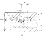
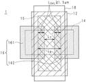
Fig. 1 is a sectional view showing a structural example of an oxide TFT 1 according to a first embodiment. The oxide TFT 1 includes a substrate 11, a bottom gate electrode 12, a gate insulating film 13, an oxide semiconductor layer 14, an etching stopper film 15, source and drain electrodes 16, a passivation film 17, and a top gate electrode 18. Fig. 2 is a plan view showing a structural example of the oxide TFT 1 according to the first embodiment. In fig. 2, the bottom gate electrode 12, the oxide semiconductor layer 14, the etching stopper film 15, the source and drain electrodes 16, and the top gate electrode 18 are shown. The source and drain electrodes 16, the top gate electrode 18, and the bottom gate electrode 12 are connected to an external circuit through contact holes (not shown).
As shown in fig. 1, in the oxide TFT 1, a bottom gate electrode 12, a gate insulating film 13, an oxide semiconductor layer 14, an etching stopper film 15, source and drain electrodes 16, a passivation film 17, and a top gate electrode 18 are laminated in this order on a substrate 11.
The substrate 11 has a rectangular plate shape. The substrate 11 is an insulating substrate such as a glass substrate.
The bottom gate electrode 12 is formed of a metal such as molybdenum (Mo), niobium (Nb), tungsten (W), aluminum (Al), chromium (Cr), copper (Cu), or silver (Ag). The bottom gate electrode 12 may be formed by laminating these metals. In addition, the bottom gate electrode 12 may be formed by using a copper alloy, an aluminum alloy, or a silver alloy. The top gate electrode 18 is also formed in the same manner as the bottom gate electrode 12.
The gate insulating film 13 is made of, for example, silicon oxide (SiO)2) Or silicon nitride (Si)3N4) And (4) forming. The gate insulating film 13 may be formed by laminating silicon oxide and silicon nitride. In addition, the gate insulating film 13 may be formed by using aluminum oxide or tantalum oxide. The etching stopper film 15 and the passivation film 17 are also formed in the same manner as the gate insulating film 13.
The oxide semiconductor layer 14 is a layer formed of an oxide semiconductor such as IGZO. IGZO is a compound of indium (In), gallium (Ga), zinc (Zn), and oxygen (O). The oxide semiconductor layer 14 may be formed of a compound of indium, zinc, and oxygen (In-Zn-O), a compound of indium, gallium, and oxygen (In-Ga-O), or a compound of indium, silicon, and oxygen (In-Si-O).
The source and drain electrodes 16 include two electrodes, an electrode 161 and an electrode 162. One of the two electrodes, the electrode 161 and the electrode 162, serves as a source electrode and the other serves as a drain electrode according to the operation state of the oxide TFT 1. That is, there are a case where the electrode 161 functions as a source electrode and the electrode 162 functions as a drain electrode, and a case where the electrode 161 functions as a drain electrode and the electrode 162 functions as a source electrode. In the following description, for simplicity, the electrode 161 is referred to as a source electrode 161, and the electrode 162 is referred to as a drain electrode 162. The source electrode 161 and the drain electrode 162 have substantially the same shape. As shown in fig. 1 and 2, the source electrode 161 and the drain electrode 162 are arranged side by side with a gap. The source and drain electrodes 16 may be formed of molybdenum, titanium, tungsten, aluminum, or the like. The source and drain electrodes 16 may be formed of molybdenum alloy, titanium alloy, aluminum alloy, copper alloy, or the like. The source and drain electrodes 16 may be formed by laminating a plurality of monomer metals or alloys.
As shown in fig. 1, in the oxide TFT 1 of the present embodiment, the length of the etching stopper film 15 in the lateral direction on the paper (hereinafter, referred to as the lateral width) is smaller than the lateral width of the oxide semiconductor layer 14. The lateral width of the gap between the source electrode 161 and the drain electrode 162 is smaller than the lateral width of the etching stopper film 15. Therefore, as shown in fig. 1, the source electrode 161 and the drain electrode 162 are stepped in the cross-sectional view. Accordingly, the oxide TFT 1 of the present embodiment is an etch stop TFT. In the oxide TFT 1, a channel layer is formed on the oxide semiconductor layer 14. In addition, in fig. 1, the lateral width of the gate electrode 12 is narrower than the lateral width of the oxide semiconductor layer 14, but is not limited thereto. The lateral width of the gate electrode 12 may be wider than the lateral width of the oxide semiconductor layer 14.
In addition, in the oxide TFT 1, the lateral width of the top gate electrode 18 is wider than the lateral width of the gap between the source electrode 161 and the drain electrode 162. The lateral width of the bottom gate electrode 12 is wider than the lateral width of the etch stop film 15. In the oxide semiconductor layer 14, a first channel region 141 is formed in a part of an interface with respect to the gate insulating film 13. More specifically, in a plan view, a region overlapping with the etching stopper film 15 on the interface is the first channel region 141. The first channel region 141 is a region in which: the carrier density can be controlled according to the voltage of the bottom gate electrode 12. In addition, in the oxide semiconductor layer 14, the second channel region 142 is formed in a part of the interface with respect to the etching stopper film 15. More specifically, a region overlapping with the gap between the source electrode 161 and the drain electrode 162 on the interface is the second channel region 142 in a plan view. The second channel region 142 is a region: the carrier density can be controlled according to the voltage of the top gate electrode 18. In the first channel region 141, the length L in the lateral direction on the paper of fig. 1 and 2BWill be referred to as a first channel length. In the second channel region 142, the length L in the lateral direction in the paper surface in fig. 1 and 2TWill be referred to as the second channel length. As shown in FIGS. 1 and 2, in the present embodimentIn the oxide TFT 1, the second channel length LTIs longer than the first channel length LBShort.
In the present embodiment, when the oxide TFT 1 configured as above is driven, a potential greater than or equal to the lower potential of the potential Vs of the source electrode 161 and the potential Vd of the drain electrode 162 is applied to the top gate electrode 18. The potential of the top gate electrode 18 is denoted by Vtg. The characteristics of the oxide TFT 1 of this embodiment are represented by the following formulas (1) and (2) or the following formulas (1) and (3).
LB>LT…(1)
Wherein the content of the first and second substances,
LB: first channel length
LT: second channel length
Vtg ≧ Vs and Vs < Vd … (2)
Vtg ≧ Vd and Vs > Vd … (3)
Wherein the content of the first and second substances,
vtg: potential of the top gate electrode 18
Vs: potential of the source electrode 161
Vd: potential of the drain electrode 162
In the oxide TFT 1, the first surface of the channel layer is in contact with the first insulating film. The channel layer is formed on the interface of the oxide semiconductor layer 14. An example of the first insulating film is the gate insulating film 13. In addition, a second surface of the channel layer is in contact with the second insulating film. An example of the second insulating film is an etching stopper film 15. Another example of the second insulating film is a passivation film 17 formed in contact with the etching stopper film 15, particularly in contact with the upper surface of the etching stopper film 15. In addition, when the oxide TFT 1 operates, a first channel region is formed on a first interface of the first insulating film with respect to the channel layer through the first gate electrode. An example of the first gate electrode is the bottom gate electrode 12. In addition, a second channel region is formed on a second interface of the second insulating film with respect to the channel layer through the second gate electrode. An example of the second gate electrode is the top gate electrode 18.
In the present embodiment, the following effects are obtained. The oxide TFT 1 is driven so that the potential Vtg of the top gate electrode 18 is greater than or equal to the lower potential of the potential Vs of the source electrode 161 and the potential Vd of the drain electrode 162. Thus, even when electric charges are generated in the oxide TFT 1, the initial characteristics are stabilized. Specifically, fluctuation of the gate voltage at which the oxide TFT 1 is switched from off to on, that is, fluctuation of the threshold voltage (sometimes referred to as threshold voltage shift due to the potential of the top gate electrode) can be suppressed.
In the operation of oxide TFTs in electronic devices such as flat panel displays and sensors, the gate electrode of the oxide TFT is positively biased with respect to the source electrode for a certain amount of time (sometimes also referred to as positive gate stress). When a positive gate stress is applied to the oxide TFT 1, in the case where the potential Vtg of the top gate electrode 18 is smaller than the lower potential of the potential Vs of the source electrode 161 and the potential Vd of the drain electrode 162, the fluctuation of the threshold voltage has a tendency to accelerate. However, in the present embodiment, Vtg is greater than or equal to the lower potential of Vs and Vd, and therefore fluctuation of the threshold voltage (sometimes also referred to as threshold voltage shift due to positive gate stress) can be suppressed. That is, the operational reliability of the oxide TFT 1 is improved.
The positive gate stress indicates a state (bias state) in which a potential greater than or equal to the potential of the source electrode or the drain electrode is applied to the gate electrode. For example, the bias state is a state in which a high-level voltage is applied to the gate electrode and a low-level voltage is applied to the source electrode or the drain electrode. It is known that the threshold voltage shifts due to positive gate stress.
Second embodiment
Fig. 3 is a sectional view showing a structural example of the oxide TFT 1 according to the second embodiment. The oxide TFT 1 includes a substrate 11, a bottom gate electrode 12, a gate insulating film 13, an oxide semiconductor layer 14, source and drain electrodes 16, a passivation film 17, and a top gate electrode 18. Fig. 4 is a plan view showing a structural example of the oxide TFT 1 according to the second embodiment. In fig. 4, the bottom gate electrode 12, the oxide semiconductor layer 14, the source and drain electrodes 16, and the top gate electrode 18 are shown. In fig. 3 and 4, the same reference numerals are applied to constituent elements having the same functions as those of the first embodiment. In the following description, differences from the first embodiment will be mainly described.
As shown in fig. 3, in the oxide TFT 1, a bottom gate electrode 12, a gate insulating film 13, an oxide semiconductor layer 14, source and drain electrodes 16, a passivation film 17, and a top gate electrode 18 are laminated in this order on a substrate 11.
The source and drain electrodes 16 include two electrodes, an electrode 161 and an electrode 162. As in the first embodiment, the electrode 161 is referred to as a source electrode 161 and the electrode 162 is referred to as a drain electrode 162 for simplicity. The source electrode 161 and the drain electrode 162 have substantially the same shape. As shown in fig. 3 and 4, the source electrode 161 and the drain electrode 162 are arranged side by side with a gap.
As shown in fig. 3, in the oxide TFT 1 of the present embodiment, the lateral width (length in the lateral direction on the paper plane) of the bottom gate electrode 12 is smaller than the lateral width of the oxide semiconductor layer 14. The lateral width of the top gate electrode 18 is smaller than the lateral width of the gap between the source electrode 161 and the drain electrode 162. In other words, the length of the top gate electrode 18 is shorter than the length between the edge of the source electrode 161 and the edge of the drain electrode 162. Accordingly, the oxide TFT 1 of this embodiment is a channel-etched TFT. In the oxide TFT 1, the oxide semiconductor layer 14 is a channel layer. The passivation film 17 is an example of the second insulating film. In this embodiment mode, the second insulating film is a single-layer film formed in a single step. In addition, in fig. 3, the lateral width of the gate electrode 12 is narrower than the lateral width of the oxide semiconductor layer 14, but is not limited thereto. The lateral width of the gate electrode 12 may be greater than the lateral width of the oxide semiconductor layer 14.
In the oxide semiconductor layer 14, a first channel region 141 is formed in a part of an interface with respect to the gate insulating film 13. More specifically, a region on the interface that overlaps with the gap between the source electrode 161 and the drain electrode 162 is the first channel region 141 in a plan view. In addition, in the oxide semiconductor layer 14, the second channel region 142 is formed in a part of an interface with the passivation film 17. More specifically, in a plan view, a region overlapping with the top gate electrode 18 on the interface is the second channel region 142.
As in the first embodiment, the channel length of the first channel region is set to the first channel length LBSetting the channel length of the second channel region to be a second channel length LT. In the present embodiment, the first channel length LBEqual to the lateral width of the gap between the source electrode 161 and the drain electrode 162. Second channel length LTEqual to the lateral width of the top gate electrode 18. In the oxide TFT 1 of this embodiment, the second channel length L is the same as that of the first embodimentTIs longer than the first channel length LBShort.
In addition, in this embodiment, when the oxide TFT 1 is driven, the potential equal to or higher than the lower potential of the potential Vs of the source electrode 161 and the potential Vd of the drain electrode 162 is applied to the top gate electrode 18, as in the first embodiment.
In the present embodiment, the following two configurations are employed as in the first embodiment. That is, 1) the second channel length L is adoptedTIs longer than the first channel length LBA short structure, and 2) a structure in which a potential greater than or equal to the lower potential of Vs and Vd is applied to the top gate electrode 18 at the time of driving. Therefore, the same effect as the first embodiment is obtained.
Third embodiment
Fig. 5 is a sectional view showing a structural example of the oxide TFT 2 according to the third embodiment. The oxide TFT 2 includes a substrate 21, a bottom gate electrode 22, a gate insulating film 23, an oxide semiconductor layer 24, an interlayer insulating film 25, a top gate electrode 26, a passivation film 27, and source and drain electrodes 28.
Fig. 6 is a plan view showing a structural example of the oxide TFT 2 according to the third embodiment. In fig. 6, the bottom gate electrode 22, the oxide semiconductor layer 24, the top gate electrode 26, and the source and drain electrodes 28 are shown.
As shown in fig. 5, in the oxide TFT 2, a bottom gate electrode 22, a gate insulating film 23, an oxide semiconductor layer 24, an interlayer insulating film 25, a top gate electrode 26, a passivation film 27, and source and drain electrodes 28 are laminated in this order on a substrate 21.
The substrate 21 has a rectangular plate shape. The substrate 21 is an insulating substrate such as a glass substrate.
The bottom gate electrode 22 and the top gate electrode 26 are formed of the same material as that of the bottom gate electrode 12 and the top gate electrode 18 of the first embodiment. The gate insulating film 23, the interlayer insulating film 25, and the passivation film 27 are formed of the same material as the gate insulating film 13 of the first embodiment. The oxide semiconductor layer 24 is formed of the same material as that of the oxide semiconductor layer 14 in the first embodiment.
The source and drain electrodes 28 include two electrodes, an electrode 281 and an electrode 282. One of the two electrodes, the electrode 281 and the electrode 282, functions as a source electrode and the other electrode functions as a drain electrode according to the operation state of the oxide TFT 2. That is, in the case where the electrode 281 functions as a source electrode and the electrode 282 functions as a drain electrode, there is a case where the electrode 281 functions as a drain electrode and the electrode 282 functions as a source electrode. In the following description, for the sake of simplicity, the electrode 281 is referred to as a source electrode 281, and the electrode 282 is referred to as a drain electrode 282. The source electrode 281 and the drain electrode 282 have substantially the same shape.
As shown in fig. 5 and 6, the source electrode 281 and the drain electrode 282 are arranged side by side with a gap. The source and drain electrodes 28 are formed of the same material as that of the source and drain electrodes 16 of the first embodiment.
As shown in fig. 5, in the oxide TFT 2 of the present embodiment, the length of the bottom gate electrode 22 in the lateral direction on the paper (hereinafter, referred to as the lateral width) is smaller than the lateral width of the top gate electrode 26. The lateral width of the gap between the source electrode 281 and the drain electrode 282 is larger than the lateral width of the top gate electrode 26. Further, the lateral width of the oxide semiconductor layer 24 is larger than the gap between the source electrode 281 and the drain electrode 282. Two contact holes are provided in the interlayer insulating film 25 and the passivation film 27. The source electrode 281 is electrically connected to the oxide semiconductor layer 24, respectively, through one of the two contact holes, and the drain electrode 282 is electrically connected to the oxide semiconductor layer 24, respectively, through the other of the two contact holes. Accordingly, the oxide TFT 2 of this embodiment is a top gate TFT. In the oxide TFT 2, a channel layer is formed on the oxide semiconductor layer 24.
In the oxide semiconductor layer 24, a first channel region 241 is formed in a part of an interface with respect to the interlayer insulating film 25. More specifically, in a plan view, a region overlapping with the top gate electrode 26 on the interface is a first channel region 241. The first channel region 241 is a region: the carrier density can be controlled according to the voltage of the top gate electrode 26. In addition, in the oxide semiconductor layer 24, a second channel region 242 is formed in a part of an interface with respect to the gate insulating film 23. More specifically, in a plan view, a region overlapping with the bottom gate electrode 22 on the interface is the second channel region 242. The second channel region 242 is a region: the carrier density can be controlled according to the voltage of the bottom gate electrode 22.
In the first channel region 241, the length in the direction in which the source electrode 281 and the drain electrode 282 are provided side by side, that is, the length L in the lateral direction on the paper surface of fig. 5 and 6TReferred to as the first channel length. In the second channel region 142, the length L in the side-by-side arrangement directionBReferred to as the second channel length. As shown in fig. 5 and 6, in the oxide TFT 2 of the present embodiment, the second channel length LBIs longer than the first channel length LTShort.
In this embodiment mode, when the oxide TFT 2 configured as above is driven, a potential greater than or equal to the lower potential of the potential Vs of the source electrode 281 and the potential Vd of the drain electrode 282 is applied to the bottom gate electrode 22. The potential of the bottom gate electrode 22 is represented by Vbg. The characteristics of the oxide TFT 2 of this embodiment as described above are represented by the following formulas (4) and (5) or the following formulas (4) and (6).
LT>LB…(4)
Wherein the content of the first and second substances,
LT: first channel length
LB: second channel length
Vbg ≧ Vs and Vs < Vd … (5)
Vbg ≧ Vd and Vs > Vd … (6)
Wherein the content of the first and second substances,
vbg: potential of bottom gate electrode 22
Vs: potential of the source electrode 281
Vd: potential of the drain electrode 282
In this embodiment, the second channel length L is determined by 1)BIs longer than the first channel length LTA short structure, and 2) a structure in which the oxide TFT 2 is driven so that the potential Vbg of the bottom gate electrode 22 is equal to or higher than the lower potential of the potential Vs of the source electrode 281 and the potential Vd of the drain electrode 282, the following effects are obtained. Even in the case where electric charges are generated on the oxide TFT 2, the initial characteristics are stable. Specifically, fluctuation of the gate voltage at which the oxide TFT 2 is switched from off to on, that is, fluctuation of the threshold voltage can be suppressed.
In addition, when a positive gate stress is applied to the oxide TFT 2, in the case where the potential Vbg of the bottom gate electrode 22 is smaller than the lower potential of the potential Vs of the source electrode 281 and the potential Vd of the drain electrode 282, fluctuation of the threshold voltage tends to be accelerated. However, in the present embodiment, Vbg is greater than or equal to the lower potential of Vs and Vd, whereby fluctuations in threshold voltage can be suppressed. That is, the operational reliability of the oxide TFT 2 is improved.
Circuit example 1
Several examples of circuits using the above-described oxide TFTs will be described below. Fig. 7 is a circuit diagram showing an example of an output stage of the gate driver. The gate driver generates a gate signal (scanning signal) in a display device or the like. In fig. 7, the bottom gate type oxide TFT 1 described in the first embodiment or the second embodiment is used as Tr1 and Tr 2. The first thin film transistor Tr1 connects the first clock signal CLK1 to the output terminal OUT 1. The second thin film transistor Tr2 connects the output terminal OUT1 to the power supply VL.
In fig. 7, for example, in the case of using a two-phase clock, a positive voltage with a duty ratio of 50% is applied to the bottom gate electrode of Tr 2. Therefore, stability against positive gate stress is required. In addition, a high voltage is applied to the bottom gate electrode of Tr1 due to the bootstrap effect, and thus the positive gate pressure becomes more severe. However, the oxide TFT 1 described in the first embodiment or the second embodiment is used as Tr1 and Tr2, and the potential applied to the top gate is set to be larger than the source potential, and therefore, stability against positive gate stress can be obtained.
Circuit example 2
Fig. 8 is a circuit diagram showing an example of a pixel circuit. Fig. 8 shows a pixel circuit of a display device in which an Organic Light Emitting Diode (OLED) is a light emitting element. An OLED is a light-emitting element including an organic light-emitting layer. The pixel circuit includes a switching tft (sw tft) and a driving tft (drive tft). The switching TFT is turned on and off according to a SCAN signal supplied through a SCAN line (SCAN). The driving TFT controls a current flowing into the OLED. In the case where the threshold voltage of the switching TFT fluctuates, there is a concern that the timing at which the OLED emits light is shifted. In addition, when the threshold voltage of the driving TFT fluctuates, there is a concern that an error occurs in the luminance of the OLED. This causes flickering of the display or degradation of the display quality of unevenness. The oxide TFT 1 described in the first embodiment or the second embodiment is used in the switching TFT and the driving TFT, and thus it is possible to contribute to the operational stability of the pixel circuit and prevent the degradation of the display quality.
Circuit example 3
Fig. 9 is a circuit diagram showing an example of the pixel circuit. Fig. 9 shows an example of a pixel circuit in a Liquid Crystal Display (LCD). In the LCD, a plurality of pixels are arranged in a two-dimensional manner, more specifically, in a matrix shape. To ensure the visibility of the figure, a circuit of 9 pixels in total by 3 pixels in the vertical direction by 3 pixels in the horizontal direction is shown. The TFTs S11 to S33 arranged in each pixel are turned on and off in accordance with scanning signals supplied from the scanning lines G1 to G3. That is, the TFT is an example of a switching element. When the TFTs are turned on, electric charges corresponding to data signals supplied from the data lines D1 to D3 are held in the storage capacitances C1 to C33. In the LCD, in the case where the threshold voltage of the TFT of each pixel fluctuates, the storage of electric charges with respect to the storage capacitor becomes insufficient (writing is insufficient). Insufficient writing of the storage capacitor causes degradation in display quality such as flicker and display unevenness.
Therefore, the oxide TFT 1 described in the first embodiment or the second embodiment is used as a TFT disposed in each pixel. Then, the potential Vtg of the top gate electrode 18 is set to be larger than the potential Vs of the source electrode 161, thereby performing control. Fig. 10 is a diagram showing an example of control of the potential of the top gate electrode 18. The horizontal axis represents time, and the vertical axis represents potential. The graph labeled Vcom represents a shift of the common potential. The graph marked Vg represents the shift of the potential Vtg of the top gate electrode 18. The graph marked with Vs represents a shift in the potential Vs of the source electrode 161. The graph labeled Vpix represents a shift in potential of a terminal on the side connected to the TFT in the storage capacitance. Vtg1 and Vtg2 denote examples of control of the potential applied to the top gate electrode 18.
The graph labeled Vtg1 is an example where the potential Vtg of the top gate electrode 18 follows the potential Vs of the source electrode. Vtg may be greater than or equal to Vs, and thus Vtg may follow Vs. The graph labeled Vtg2 is an example where the potential Vtg of the top gate electrode 18 is kept constant. In the case where Vtg is held at the maximum value of the source potential Vs, Vtg is greater than or equal to Vs. The maximum value of Vs can be found by calculating a theoretical value in design or by actual measurement. In addition, in consideration of an error, a potential slightly larger than the obtained potential may be used as Vtg.
The oxide TFT 1 described in the first embodiment or the second embodiment is used in a pixel circuit of an LCD, and thus can contribute to the operational stability of the pixel circuit and prevent the degradation of display quality.
In circuit example 1 to circuit example 3, only a circuit example using a bottom gate type TFT is explained, but the example is not limited thereto. The oxide TFT 2 described in the third embodiment can be used in a circuit example using a top gate type TFT. In this case, the same effects as those obtained above are obtained.
Fourth embodiment
In this embodiment, design conditions are added to the oxide TFT 1 described in the first embodiment. Fig. 11 is a plan view showing a structural example of the oxide TFT 1 according to the fourth embodiment. In fig. 11, the same components as those of the first embodiment are denoted by the same reference numerals as those of the first embodiment. The oxide TFT 1 of this embodiment is an etch stop TFT. It is different from the first embodiment in that,a first channel length L is setB10 micrometers (μm), and a channel width W of 10 μm or less.
W/L is known as one of parameters representing characteristics of a transistor. W is the channel width and L is the channel length. In the present embodiment, the channel length is the first channel length LB. Fabricating a first channel length LBA plurality of oxide TFTs 1 set to 10 μm and varying the channel width W. In the plurality of oxide TFTs having different channel widths W, fluctuation in threshold voltage due to positive gate stress is measured, whereby good results are obtained as W decreases. Therefore, as the channel width W decreases, operational stability is obtained. I.e. the first channel length LBIn the case of setting to 10 micrometers, it is desirable that the channel width W be set to 10 micrometers or less.
According to the present embodiment, this condition is added to the channel width W, whereby the operational stability with respect to the positive gate stress can be more reliably obtained in the oxide TFT 1. Further, a condition of setting the channel width W smaller is a condition favorable for the TFT driving the OLED.
Fifth embodiment
In this embodiment, design conditions are added to the oxide TFT 1 described in the first embodiment. Fig. 12A and 12B are explanatory diagrams showing a structural example of the oxide TFT 1 according to the fifth embodiment. Fig. 12A is a plan view showing a structural example of the oxide TFT 1. Fig. 12B is a sectional view showing a structural example of the oxide TFT 1. In fig. 12A and 12B, the same reference numerals as those of the first embodiment are applied to the same structures as those of the first embodiment. The oxide TFT 1 of this embodiment is an etch stop TFT. It is different from the first embodiment in that the following conditions are set: a width (hereinafter, overlap width) L of a region where the first channel region overlaps with the source electrode 161 in a plan viewOVLGreater than or equal to 1.5 micrometers. This also applies to the width of the region where the first channel region overlaps with the drain electrode 162. In other words, the overlap width is the length in the channel length direction in which the etching stopper film 15 overlaps the source electrode 161, and the etching stopper film 15 overlaps the drain electrode 162The length of the stack in the channel length direction.
It is considered that the operation stability of the oxide TFT 1 is based on the first channel length LBAnd a second channel length LTThe difference between them. Therefore, as the difference increases, an effect is obtained. In the overlapping width LOVLIncreased second channel length LTAnd decreases. At the overlapping width LOVLAt the increased condition, the first channel length LBAnd is not changed. Therefore, it can be said that the first channel length LBAnd a second channel length LTThe difference therebetween increases, whereby the operation stability of the oxide TFT 1 improves. In the oxide TFT 1, at the first channel length LBWhen the thickness is 10 μm, the overlap width L is preferably setOVLIs set to be greater than or equal to 1.5 micrometers.
According to the present embodiment, the overlapping width LOVLThis condition is added, whereby the operation stability against positive gate stress can be more reliably obtained in the oxide TFT 1. Further, the width L of the overlap will be overlappedOVLSetting to a larger condition is a condition favorable for a TFT requiring an increase in the channel width W.
Sixth embodiment
In this embodiment, the oxide TFT 1 described in the second embodiment is added with design conditions. Fig. 13A and 13B are explanatory diagrams showing a structural example of the oxide TFT 1 according to the sixth embodiment. Fig. 13A is a plan view showing a structural example of the oxide TFT 1. Fig. 13B is a sectional view showing a structural example of the oxide TFT 1. In fig. 13A and 13B, the same reference numerals as those of the second embodiment are applied to the same structures as those of the second embodiment. The oxide TFT 1 of this embodiment is a channel-etched TFT. This is different from the second embodiment in that the following conditions are set: a distance (hereinafter, gap width) L of the gap between the source electrode 161 and the top gate electrode 18 in a plan viewOFFAnd the distance of the gap between the drain electrode 162 and the top gate electrode 18 is greater than or equal to 1.5 micrometers.
It is considered that the operation stability of the oxide TFT 1 is based on the first channel length LBAnd a second channel length LTThe difference between them. Therefore, as the difference is larger, an effect is obtained. On the basis of the restriction that the distance of the gap between the source electrode 161 and the drain electrode 162 is constant, the gap width L is set to be constantOFFIncreased second channel length LTAnd decrease. At the gap width LOFFAt the increased condition, the first channel length LBAnd is not changed. Therefore, it can be said that the first channel length LBAnd a second channel length LTThe difference therebetween increases, whereby the operation stability of the oxide TFT 1 improves. In the oxide TFT 1, at the first channel length LBWhen the gap width is set to 10 μm, the gap width L is preferably set toOFFIs set to be greater than or equal to 1.5 micrometers.
According to the present embodiment, the gap width LOFFThis condition is added, whereby the operation stability against the positive gate stress can be more reliably obtained in the oxide TFT 1. Further, the gap width L is setOFFSetting to a larger condition is a condition favorable for a TFT requiring an increase in the channel width W.
Seventh embodiment
In the oxide TFT 1 of the present embodiment, design conditions are added to the oxide TFT 1 of the first embodiment. Fig. 14A and 14B are explanatory diagrams showing a structural example of the oxide TFT 1 according to the seventh embodiment. Fig. 14A is a plan view showing a structural example of the oxide TFT 1. Fig. 14B is a cross-sectional view taken along line XIV-XIV of fig. 14A. In fig. 14A and 14B, the same reference numerals as those of the first embodiment are applied to the same structures as those of the first embodiment. The oxide TFT 1 of this embodiment is an etch stop TFT. It is different from the first embodiment in that the following conditions are set: a width (hereinafter, source wrap-around width) L of a region where the first channel region overlaps with the source electrode 161 in a plan viewSOVLA width L of a region overlapping with the drain electrode 162 (hereinafter, drain wrap-around width) than the first channel regionDOVLLarge conditions.
In the present embodiment, a portion where the layer constituting the bottom gate electrode 12 overlaps the layer constituting the source electrode 161 in a plan view is formed, and thus the capacitor Cst is formed between the bottom gate electrode 12 and the source electrode 161. Fig. 14A and 14B illustrate two elements of the oxide TFT 1 and the capacitor Cst. The terminal tm1 denotes a terminal connected to the gate electrode 12 and the capacitor Cst, and the terminal tm2 denotes a terminal connected to the drain electrode.
Fig. 15A and 15B are circuit diagrams showing a circuit example using the oxide TFT 1. Fig. 15A shows a circuit example of an output stage of the gate driver. Fig. 15B shows an example of a pixel circuit of an OLED. The Tr3 and the capacitor Cst shown in fig. 15A can be implemented by the structures shown in fig. 14A and 14B. In addition, Tr4 and the capacitor Cst shown in fig. 15B can also be realized by the structures shown in fig. 14A and 14B. Terminals tm1 and tm2 shown in fig. 15A and 15B correspond to terminals tm1 and tm2 shown in fig. 14A and 14B. In the case where the oxide TFT 1 of this embodiment is used as Tr3 and Tr4, the oxide TFT 1 and the capacitor Cst can be efficiently manufactured according to the structures shown in fig. 14A and 14B.
In addition, in the oxide TFT 1, the source winding width L on the source side connected to the capacitor Cst is increased by increasing the source winding width LSOVLThe following effects are obtained. As with the other embodiments described above, the operational stability against positive gate stress is improved. In addition, the source winding width LSOVLAnd thus the area functioning as the capacitor Cst increases. Accordingly, a planar area required for the structure of the capacitor Cst can be reduced, and thus a planar area required for the structure of the combination of the oxide TFT 1 and the capacitor Cst can be reduced.
The planar area required for the structure of the oxide TFT 1 combined with the capacitor Cst in the case of the pixel circuit for the OLED is reduced, whereby the aperture ratio is improved. In addition, each pixel can be reduced, and thus the definition of the display can be improved.
Example of drive Circuit
Next, a driving circuit of the oxide TFT 1 will be explained. Fig. 16 is a circuit diagram showing an example of the drive circuit 100. The drive circuit 100 includes a TFT circuit 101 and an application circuit 102. The TFT circuit 101 is a circuit including an oxide TFT 1. The structure of the TFT circuit 101 is appropriately designed according to the use of the oxide TFT 1. In addition, the same structure can be applied to the driver circuit of the oxide TFT 2.
The applying circuit 102 is a circuit that generates a potential to be applied to the top gate electrode 18 of the oxide TFT 1. The applying circuit 102 includes a comparator 1021, a switch 1022, and a buffer 1023. The comparator 1021 determines the magnitude relationship between Vs and Vd. Vs is the potential of the source electrode 161 of the oxide TFT 1. Vd is the potential of the drain electrode 162 of the oxide TFT 1. The switch 1022 is a changeover switch. Vs and Vd are input to the switch 1022, and one of Vs and Vd is output from the switch 1022. The switching of the switch 1022 is controlled based on the output of the comparator 1021. The switch 1022 outputs the lower potential of Vs and Vd according to the control of the comparator 1021. The buffer 1023 inputs the output of the switch 1022 to the TFT circuit 101. This input is applied to the top gate electrode 18 of the oxide TFT 1. In addition, the buffer 1023 may be replaced with an amplifier.
One application circuit 102 is provided on each oxide TFT 1, but the number of application circuits 102 is not limited to this. In the case where the circuit includes a plurality of oxide TFTs 1 but the plurality of oxide TFTs 1 do not operate at the same time, one applying circuit 102 may be provided. In addition, in the case where the plurality of oxide TFTs 1 are simultaneously operated, one applying circuit 102 may be provided in design under the same operating condition. That is, there is a case where all potentials to be applied to the top gate electrode 18 of the oxide TFT 1 to be operated can be the same potential in design. In this case, Vs and Vd are set as inputs of the application circuit 102 for one oxide TFT 1 among the oxide TFTs 1 that operate simultaneously. The output of the applying circuit 102 is applied to the top gate electrodes of all the oxide TFTs that operate. In addition, when the potential to be applied to the top gate electrode 18 of the oxide TFT 1 can be uniquely determined in design, the application circuit 102 is set to a constant voltage source. In this case, a constant potential is applied to the top gate electrode 18.
In the above description, the cross-sectional views are referred to for explaining the order of lamination of the layers, and the thickness or size of each layer and the dimension (size relationship) of the thickness between the layers are not limited to the illustrated forms.
The technical features (structural requirements) described in the respective embodiments can be combined with each other, and new technical features can be formed by the combination.
The embodiments disclosed herein are exemplary in all respects and are not necessarily to be considered as limiting. The scope of the invention is not limited to the above description but is indicated by the claims, and is intended to include all equivalents of the claims and all modifications within the claims.
Claims (17)
1. A thin film transistor, comprising:
a source electrode and a drain electrode;
a channel layer formed of an oxide semiconductor, the channel layer being in contact with the source electrode and the drain electrode;
a first insulating film and a first gate electrode formed on a first surface side of the channel layer, the first surface side not being in contact with the source electrode and the drain electrode;
a first channel region formed on a first interface between the channel layer and the first insulating film from an edge where the source electrode and the channel layer contact each other to an edge where the drain electrode and the channel layer contact each other;
a second insulating film and a second gate electrode formed on a second surface side of the channel layer, the second surface side being in contact with the source electrode and the drain electrode; and
a second channel region formed on a second interface between the channel layer and the second insulating film, the second channel region being formed by removing a region where the source electrode and the drain electrode overlap with the channel layer from a region where the second gate electrode overlaps with the channel layer,
wherein the source electrode and the drain electrode are arranged side by side with a gap therebetween,
when the length of the first channel region in the direction in which the source electrode and the drain electrode are arranged side by side is set to a first channel length and the length of the second channel region in the direction in which the source electrode and the drain electrode are arranged side by side is set to a second channel length,
the second channel length is shorter than the first channel length, and
the potential applied to the second gate electrode is greater than or equal to the lower of the potentials of the source electrode and the drain electrode.
2. The thin film transistor of claim 1,
the thin film transistor is an etching stop type transistor, wherein the second insulating film is composed of an etching stop film in contact with the second surface side of the channel layer and a passivation film in contact with an upper surface of the etching stop film.
3. The thin film transistor of claim 2,
a length of the etching stopper film overlapping with the source electrode in a channel length direction and a length of the etching stopper film overlapping with the drain electrode in the channel length direction are each greater than or equal to 1.5 micrometers.
4. The thin film transistor of claim 3,
a length of the etching stopper film overlapping with the source electrode in the channel length direction is longer than a length of the etching stopper film overlapping with the drain electrode in the channel length direction.
5. The thin film transistor of claim 1,
the thin film transistor is a channel-etched transistor, wherein the second insulating film is a passivation film in contact with the second surface side of the channel layer, and
the length of the second gate electrode is shorter than the length between the edge of the source electrode and the edge of the drain electrode.
6. The thin film transistor of claim 5,
a length from the edge of the source electrode and the edge of the drain electrode to an edge of the second gate electrode is greater than or equal to 1.5 micrometers.
7. The thin film transistor of claim 1, wherein a lateral width of the first channel region is shorter than a lateral width of the first gate electrode.
8. The thin film transistor according to any one of claims 1 to 7,
the channel width is less than or equal to 10 microns.
9. A thin film transistor, comprising:
a first gate electrode, a first insulating film, a channel layer composed of an oxide semiconductor, a second insulating film, a second gate electrode, a passivation film, a source electrode, and a drain electrode formed in this order,
a first channel region in which the first gate electrode and the channel layer overlap on a first interface between the channel layer and the first insulating film; and
a second channel region in which the second gate electrode and the channel layer overlap on a second interface between the channel layer and the second insulating film;
wherein the source electrode and the drain electrode are in contact with a channel layer region excluding the second channel region and are arranged side by side with a gap therebetween,
when the length of the first channel region in the direction in which the source electrode and the drain electrode are arranged side by side is set to a first channel length and the length of the second channel region in the direction in which the source electrode and the drain electrode are arranged side by side is set to a second channel length,
the second channel length is longer than the first channel length, and
the potential applied to the first gate electrode is greater than or equal to the lower potential of the potentials of the source electrode and the drain electrode.
10. The thin film transistor of claim 9,
the channel width is less than or equal to 10 microns.
11. A display device, comprising:
a plurality of pixels which respectively include a switching element having the thin film transistor according to any one of claims 1 to 10 and a display element, and which are arranged in a two-dimensional manner; and
an applying circuit that applies a lower potential of potentials of the source electrode and the drain electrode of the switching element to the second gate electrode of the switching element.
12. A transistor circuit comprising a plurality of thin film transistors, wherein each of the plurality of thin film transistors is a thin film transistor according to any one of claims 1 to 10.
13. The transistor circuit of claim 12, comprising:
a first thin film transistor composed of the thin film transistor connects a first clock signal to an output terminal; and
a second thin film transistor constituted by the thin film transistor connects the output terminal to a power supply.
14. The transistor circuit of claim 12, further comprising:
a light-emitting element including an organic light-emitting layer;
a capacitor;
wherein:
a driving transistor configured by the thin film transistor causes a current corresponding to a voltage of the capacitor to flow into the light emitting element; and
a switching transistor constituted by the thin film transistor controls the operation of the driving transistor.
15. A driving method of a thin film transistor, comprising:
detecting a potential of a source electrode and a potential of a drain electrode of the thin film transistor according to any one of claims 1 to 10;
determining a lower potential of the detected potential of the source electrode and the detected potential of the drain electrode,
generating a potential greater than or equal to the determined potential; and
applying the generated potential to a second gate electrode of the thin film transistor.
16. The driving method of the thin film transistor according to claim 15, further comprising:
driving a first thin film transistor configured by the thin film transistor connecting a first clock signal to an output terminal and a second thin film transistor configured by the thin film transistor connecting the output terminal to a power supply.
17. The driving method of the thin film transistor according to claim 15, further comprising:
a driving capacitor, a driving transistor composed of the thin film transistor, and a switching transistor composed of the thin film transistor, the driving transistor flowing a current corresponding to a voltage of the capacitor into an organic light emitting layer, and the switching transistor controlling an operation of the driving transistor.
Applications Claiming Priority (2)
| Application Number | Priority Date | Filing Date | Title |
|---|---|---|---|
| JP2016241604A JP6822114B2 (en) | 2016-12-13 | 2016-12-13 | How to drive display devices, transistor circuits and thin film transistors |
| JP2016-241604 | 2016-12-13 |
Publications (2)
| Publication Number | Publication Date |
|---|---|
| CN108231904A CN108231904A (en) | 2018-06-29 |
| CN108231904B true CN108231904B (en) | 2022-05-13 |
Family
ID=62489696
Family Applications (1)
| Application Number | Title | Priority Date | Filing Date |
|---|---|---|---|
| CN201711190146.7A Active CN108231904B (en) | 2016-12-13 | 2017-11-24 | Thin film transistor, driving method thereof, display device and transistor circuit |
Country Status (3)
| Country | Link |
|---|---|
| US (1) | US10388798B2 (en) |
| JP (1) | JP6822114B2 (en) |
| CN (1) | CN108231904B (en) |
Families Citing this family (20)
| Publication number | Priority date | Publication date | Assignee | Title |
|---|---|---|---|---|
| KR102420080B1 (en) * | 2017-05-19 | 2022-07-13 | 삼성디스플레이 주식회사 | Multi-channel TFT and Pixel comprising the TFT |
| JP6844845B2 (en) | 2017-05-31 | 2021-03-17 | 三国電子有限会社 | Display device |
| KR20200000513A (en) * | 2018-06-22 | 2020-01-03 | 삼성디스플레이 주식회사 | Organic light emitting diode display device |
| JP7190729B2 (en) | 2018-08-31 | 2022-12-16 | 三国電子有限会社 | ORGANIC ELECTROLUMINESCENT DEVICE HAVING CARRIER INJECTION CONTROL ELECTRODE |
| WO2020059027A1 (en) * | 2018-09-18 | 2020-03-26 | シャープ株式会社 | Display device |
| JP7246681B2 (en) | 2018-09-26 | 2023-03-28 | 三国電子有限会社 | TRANSISTOR, TRANSISTOR MANUFACTURING METHOD, AND DISPLAY DEVICE INCLUDING TRANSISTOR |
| US20220093650A1 (en) * | 2019-02-04 | 2022-03-24 | Sharp Kabushiki Kaisha | Display device |
| JP7190740B2 (en) | 2019-02-22 | 2022-12-16 | 三国電子有限会社 | Display device having an electroluminescence element |
| TWI691762B (en) * | 2019-04-18 | 2020-04-21 | 友達光電股份有限公司 | Pixel structure |
| KR20200143618A (en) * | 2019-06-14 | 2020-12-24 | 삼성디스플레이 주식회사 | Gate driver and display device including the same |
| US11121263B2 (en) * | 2019-08-27 | 2021-09-14 | Apple Inc. | Hydrogen trap layer for display device and the same |
| US11915647B2 (en) * | 2019-10-02 | 2024-02-27 | Shar Kabushiki Kaisha | Display device equipped with current-driven electro-optical elements |
| CN110993620A (en) * | 2019-12-05 | 2020-04-10 | 深圳市华星光电半导体显示技术有限公司 | Array substrate, preparation method thereof and display panel |
| JP7444436B2 (en) | 2020-02-05 | 2024-03-06 | 三国電子有限会社 | liquid crystal display device |
| KR20220042031A (en) * | 2020-09-25 | 2022-04-04 | 삼성디스플레이 주식회사 | Gate driving circuit and display apparatus including the same |
| CN112289854B (en) * | 2020-10-22 | 2021-09-24 | 深圳市华星光电半导体显示技术有限公司 | Array substrate and preparation method thereof |
| CN112530978B (en) * | 2020-12-01 | 2024-02-13 | 京东方科技集团股份有限公司 | Switching device structure, preparation method thereof, thin film transistor film layer and display panel |
| CN112490275B (en) * | 2020-12-03 | 2023-04-21 | 湖北长江新型显示产业创新中心有限公司 | Display panel, manufacturing method thereof and display device |
| KR20230051974A (en) * | 2021-10-12 | 2023-04-19 | 엘지디스플레이 주식회사 | Thin film transistor and display apparatus comprising the same |
| TWI802478B (en) * | 2022-07-27 | 2023-05-11 | 友達光電股份有限公司 | Active component substrate |
Citations (5)
| Publication number | Priority date | Publication date | Assignee | Title |
|---|---|---|---|---|
| JP2007173741A (en) * | 2005-12-26 | 2007-07-05 | Sharp Corp | P-type thin-film transistor, n-type thin-film transistor and semiconductor device |
| JP2008083171A (en) * | 2006-09-26 | 2008-04-10 | Casio Comput Co Ltd | Pixel drive circuit and image display apparatus |
| CN102315278A (en) * | 2010-07-07 | 2012-01-11 | 三星移动显示器株式会社 | Double grid thin-film transistor and comprise the OLED display unit of double grid thin-film transistor |
| CN105282462A (en) * | 2014-07-23 | 2016-01-27 | Nlt科技股份有限公司 | Image sensor and driving method thereof |
| WO2016192624A1 (en) * | 2015-06-04 | 2016-12-08 | 昆山工研院新型平板显示技术中心有限公司 | Thin film transistor and manufacturing method thereof |
Family Cites Families (11)
| Publication number | Priority date | Publication date | Assignee | Title |
|---|---|---|---|---|
| JP4257971B2 (en) * | 2003-03-27 | 2009-04-30 | 独立行政法人産業技術総合研究所 | Method for applying gate signal of double gate field effect transistor |
| JP2009133914A (en) * | 2007-11-28 | 2009-06-18 | Sony Corp | Display apparatus |
| US8586979B2 (en) * | 2008-02-01 | 2013-11-19 | Samsung Electronics Co., Ltd. | Oxide semiconductor transistor and method of manufacturing the same |
| US8681307B2 (en) * | 2008-12-19 | 2014-03-25 | Sharp Kabushiki Kaisha | Insulated gate transistor, active matrix substrate, liquid crystal display device, and method for producing the same |
| WO2011048923A1 (en) * | 2009-10-21 | 2011-04-28 | Semiconductor Energy Laboratory Co., Ltd. | E-book reader |
| DE112011102837B4 (en) * | 2010-08-27 | 2021-03-11 | Semiconductor Energy Laboratory Co., Ltd. | Memory device and semiconductor device with double gate and oxide semiconductor |
| US20120298999A1 (en) * | 2011-05-24 | 2012-11-29 | Sharp Kabushiki Kaisha | Semiconductor device and manufacturing method thereof |
| KR102044667B1 (en) * | 2013-05-28 | 2019-11-14 | 엘지디스플레이 주식회사 | Flat panel display device having oxide thin film transistor and method for fabricating thereof |
| KR20150061302A (en) * | 2013-11-27 | 2015-06-04 | 삼성디스플레이 주식회사 | Display substrates, methods of manufacturing the same and display devices including the same |
| JP6350984B2 (en) * | 2014-04-24 | 2018-07-04 | Tianma Japan株式会社 | Thin film transistor and display device |
| US10439069B2 (en) * | 2015-08-10 | 2019-10-08 | Nlt Technologies, Ltd. | Optical sensor element and photoelectric conversion device |
-
2016
- 2016-12-13 JP JP2016241604A patent/JP6822114B2/en active Active
-
2017
- 2017-11-24 CN CN201711190146.7A patent/CN108231904B/en active Active
- 2017-12-01 US US15/828,586 patent/US10388798B2/en active Active
Patent Citations (5)
| Publication number | Priority date | Publication date | Assignee | Title |
|---|---|---|---|---|
| JP2007173741A (en) * | 2005-12-26 | 2007-07-05 | Sharp Corp | P-type thin-film transistor, n-type thin-film transistor and semiconductor device |
| JP2008083171A (en) * | 2006-09-26 | 2008-04-10 | Casio Comput Co Ltd | Pixel drive circuit and image display apparatus |
| CN102315278A (en) * | 2010-07-07 | 2012-01-11 | 三星移动显示器株式会社 | Double grid thin-film transistor and comprise the OLED display unit of double grid thin-film transistor |
| CN105282462A (en) * | 2014-07-23 | 2016-01-27 | Nlt科技股份有限公司 | Image sensor and driving method thereof |
| WO2016192624A1 (en) * | 2015-06-04 | 2016-12-08 | 昆山工研院新型平板显示技术中心有限公司 | Thin film transistor and manufacturing method thereof |
Also Published As
| Publication number | Publication date |
|---|---|
| JP6822114B2 (en) | 2021-01-27 |
| CN108231904A (en) | 2018-06-29 |
| US20180166585A1 (en) | 2018-06-14 |
| JP2018098364A (en) | 2018-06-21 |
| US10388798B2 (en) | 2019-08-20 |
Similar Documents
| Publication | Publication Date | Title |
|---|---|---|
| CN108231904B (en) | Thin film transistor, driving method thereof, display device and transistor circuit | |
| US10121406B2 (en) | Shift register using oxide transistor and display device using the same | |
| US11417774B2 (en) | Thin film transistor, gate driver including the same, and display device including the gate driver | |
| JP5581151B2 (en) | Display device and electronic device | |
| JP5383160B2 (en) | Liquid crystal display device, display module, and electronic device | |
| US7531837B2 (en) | Multi-channel thin film transistor structure | |
| CN101861615A (en) | Thin-film transistor circuit, driving method thereof, and light-emitting display apparatus | |
| WO2017094682A1 (en) | Semiconductor device, and method for manufacturing same | |
| KR20210016111A (en) | Display device | |
| WO2023015622A1 (en) | Display panel and mobile terminal | |
| CN112331674A (en) | Display device and method for manufacturing the same | |
| US9418594B2 (en) | Display device | |
| US20200185379A1 (en) | Active matrix substrate and method of manufacturing same | |
| CN112216705A (en) | Thin film transistor substrate | |
| US9484466B2 (en) | Thin film transistor | |
| US20180277574A1 (en) | Active matrix substrate and method for producing the same | |
| US20200118506A1 (en) | Active matrix substrate and demultiplexer circuit | |
| US8462287B2 (en) | Active matrix substrate and display device using the same | |
| CN112086061A (en) | Display device | |
| US11710746B2 (en) | Semiconductor device and display device | |
| US20230145843A1 (en) | Display device | |
| CN219716870U (en) | Display apparatus | |
| EP4283682A1 (en) | Display device and manufacturing method thereof | |
| US20240090276A1 (en) | Display panel and display device | |
| CN114497076A (en) | Display device |
Legal Events
| Date | Code | Title | Description |
|---|---|---|---|
| PB01 | Publication | ||
| PB01 | Publication | ||
| SE01 | Entry into force of request for substantive examination | ||
| SE01 | Entry into force of request for substantive examination | ||
| TA01 | Transfer of patent application right | ||
| TA01 | Transfer of patent application right |
Effective date of registration: 20191125 Address after: 1918 Tianma Building, Liuxian Avenue, Beizhan community, Minzhi street, Longhua District, Shenzhen City, Guangdong Province Applicant after: Tianma Microelectronics Co., Ltd. Address before: Kanagawa Prefecture, Japan Applicant before: Tianma Japan Corporation |
|
| GR01 | Patent grant | ||
| GR01 | Patent grant |