CN107979552B - Apparatus and method for Single Antenna Interference Cancellation (SAIC) enhancement - Google Patents
Apparatus and method for Single Antenna Interference Cancellation (SAIC) enhancement Download PDFInfo
- Publication number
- CN107979552B CN107979552B CN201710702781.2A CN201710702781A CN107979552B CN 107979552 B CN107979552 B CN 107979552B CN 201710702781 A CN201710702781 A CN 201710702781A CN 107979552 B CN107979552 B CN 107979552B
- Authority
- CN
- China
- Prior art keywords
- output
- processor
- interference cancellation
- signal
- channel
- Prior art date
- Legal status (The legal status is an assumption and is not a legal conclusion. Google has not performed a legal analysis and makes no representation as to the accuracy of the status listed.)
- Active
Links
Images
Classifications
-
- H—ELECTRICITY
- H04—ELECTRIC COMMUNICATION TECHNIQUE
- H04B—TRANSMISSION
- H04B1/00—Details of transmission systems, not covered by a single one of groups H04B3/00 - H04B13/00; Details of transmission systems not characterised by the medium used for transmission
- H04B1/06—Receivers
- H04B1/10—Means associated with receiver for limiting or suppressing noise or interference
-
- H—ELECTRICITY
- H04—ELECTRIC COMMUNICATION TECHNIQUE
- H04L—TRANSMISSION OF DIGITAL INFORMATION, e.g. TELEGRAPHIC COMMUNICATION
- H04L25/00—Baseband systems
- H04L25/02—Details ; arrangements for supplying electrical power along data transmission lines
- H04L25/03—Shaping networks in transmitter or receiver, e.g. adaptive shaping networks
- H04L25/03006—Arrangements for removing intersymbol interference
-
- H—ELECTRICITY
- H04—ELECTRIC COMMUNICATION TECHNIQUE
- H04L—TRANSMISSION OF DIGITAL INFORMATION, e.g. TELEGRAPHIC COMMUNICATION
- H04L25/00—Baseband systems
- H04L25/02—Details ; arrangements for supplying electrical power along data transmission lines
- H04L25/06—Dc level restoring means; Bias distortion correction ; Decision circuits providing symbol by symbol detection
- H04L25/061—Dc level restoring means; Bias distortion correction ; Decision circuits providing symbol by symbol detection providing hard decisions only; arrangements for tracking or suppressing unwanted low frequency components, e.g. removal of dc offset
-
- H—ELECTRICITY
- H04—ELECTRIC COMMUNICATION TECHNIQUE
- H04B—TRANSMISSION
- H04B7/00—Radio transmission systems, i.e. using radiation field
- H04B7/02—Diversity systems; Multi-antenna system, i.e. transmission or reception using multiple antennas
- H04B7/04—Diversity systems; Multi-antenna system, i.e. transmission or reception using multiple antennas using two or more spaced independent antennas
- H04B7/0413—MIMO systems
-
- H—ELECTRICITY
- H04—ELECTRIC COMMUNICATION TECHNIQUE
- H04L—TRANSMISSION OF DIGITAL INFORMATION, e.g. TELEGRAPHIC COMMUNICATION
- H04L1/00—Arrangements for detecting or preventing errors in the information received
- H04L1/004—Arrangements for detecting or preventing errors in the information received by using forward error control
- H04L1/0045—Arrangements at the receiver end
- H04L1/0054—Maximum-likelihood or sequential decoding, e.g. Viterbi, Fano, ZJ algorithms
-
- H—ELECTRICITY
- H04—ELECTRIC COMMUNICATION TECHNIQUE
- H04L—TRANSMISSION OF DIGITAL INFORMATION, e.g. TELEGRAPHIC COMMUNICATION
- H04L25/00—Baseband systems
- H04L25/02—Details ; arrangements for supplying electrical power along data transmission lines
- H04L25/03—Shaping networks in transmitter or receiver, e.g. adaptive shaping networks
- H04L25/03006—Arrangements for removing intersymbol interference
- H04L25/03178—Arrangements involving sequence estimation techniques
- H04L25/03248—Arrangements for operating in conjunction with other apparatus
- H04L25/0328—Arrangements for operating in conjunction with other apparatus with interference cancellation circuitry
-
- H—ELECTRICITY
- H04—ELECTRIC COMMUNICATION TECHNIQUE
- H04L—TRANSMISSION OF DIGITAL INFORMATION, e.g. TELEGRAPHIC COMMUNICATION
- H04L25/00—Baseband systems
- H04L25/02—Details ; arrangements for supplying electrical power along data transmission lines
- H04L25/03—Shaping networks in transmitter or receiver, e.g. adaptive shaping networks
- H04L25/03006—Arrangements for removing intersymbol interference
- H04L25/03821—Inter-carrier interference cancellation [ICI]
-
- H—ELECTRICITY
- H04—ELECTRIC COMMUNICATION TECHNIQUE
- H04L—TRANSMISSION OF DIGITAL INFORMATION, e.g. TELEGRAPHIC COMMUNICATION
- H04L27/00—Modulated-carrier systems
- H04L27/01—Equalisers
-
- H—ELECTRICITY
- H04—ELECTRIC COMMUNICATION TECHNIQUE
- H04L—TRANSMISSION OF DIGITAL INFORMATION, e.g. TELEGRAPHIC COMMUNICATION
- H04L27/00—Modulated-carrier systems
- H04L27/18—Phase-modulated carrier systems, i.e. using phase-shift keying
- H04L27/20—Modulator circuits; Transmitter circuits
- H04L27/2003—Modulator circuits; Transmitter circuits for continuous phase modulation
- H04L27/2007—Modulator circuits; Transmitter circuits for continuous phase modulation in which the phase change within each symbol period is constrained
- H04L27/2017—Modulator circuits; Transmitter circuits for continuous phase modulation in which the phase change within each symbol period is constrained in which the phase changes are non-linear, e.g. generalized and Gaussian minimum shift keying, tamed frequency modulation
-
- H—ELECTRICITY
- H04—ELECTRIC COMMUNICATION TECHNIQUE
- H04L—TRANSMISSION OF DIGITAL INFORMATION, e.g. TELEGRAPHIC COMMUNICATION
- H04L25/00—Baseband systems
- H04L25/02—Details ; arrangements for supplying electrical power along data transmission lines
- H04L25/03—Shaping networks in transmitter or receiver, e.g. adaptive shaping networks
- H04L25/03006—Arrangements for removing intersymbol interference
- H04L2025/03592—Adaptation methods
- H04L2025/03598—Algorithms
Abstract
An Interference Cancellation (IC) processor, a method of manufacturing a semiconductor device, and a method of constructing an integrated circuit are provided. The IC processor includes a plurality of single-tone interference cancellation (MIC) filter estimation processors, wherein each MIC filter estimation processor includes a different equalizer offset k0And an input for receiving the derotated signal and providing an effective channel hres,iAnd estimated filter pi(ii) a A plurality of filters, wherein each filter comprises an input connected to the plurality of MIC filter estimation processors and an output; a plurality of multipliers, wherein each multiplier comprises an output, a first input connected to the plurality of filters, and a second input for receiving a weight; a branch combiner comprising a plurality of inputs connected to the plurality of multipliers for providing a combined residual channel HresAnd a second output for providing a projected output y of the derotated signal.
Description
This application claims priority from U.S. provisional patent application serial No. 62/411,336 filed at USPTO on 21/10 in 2016 and U.S. non-provisional patent application serial No. 15/381,970 filed at USPTO on 16/12 in 2016, the entire contents of which are incorporated herein by reference.
Technical Field
The present disclosure relates generally to communication technology and, more particularly, to an apparatus and method for Single Antenna Interference Cancellation (SAIC).
Background
In communication networks, such as second generation (2G) global system for mobile communications (GSM) networks, system capacity is typically limited by co-channel interference (CCI) due to channel reuse.
GSM uses a combination of Time Division Multiple Access (TDMA) and Frequency Division Multiple Access (FDMA). Gaussian Minimum Shift Keying (GMSK) modulation is used in GSM to make unwanted or spurious emissions outside the nominal bandwidth low enough that adjacent channels can be used from the same base station.
Using the TDMA scheme, data transmitted by a carrier is provided to up to 8 different users by dividing the carrier into 8 time slots. This enables different users of a single Radio Frequency (RF) channel to be allocated in different time slots. Different users can then use the same RF channel without interfering with each other. A GSM burst is a transmission in a time slot, wherein the burst comprises: 3 tail bits at the beginning of a GSM burst to provide the transmitter with time to power up it, 57 data bits to carry information, 1 marker bit to indicate the type of data in the previous field, 26 bits for the Training Sequence (TS) (used as a timing reference) and for equalization, 1 marker bit to indicate the type of data in the data field, 57 data bits, 3 tail bits to provide the transmitter with time to power down it, and 8.25 bits at the end of GSM to provide guard time.
The basic GSM receiver treats the CCI only as Additive White Gaussian Noise (AWGN), resulting in poor performance. Unlike white gaussian noise, which is uncorrelated in both time and space, interference is usually strongly correlated in both time and space, i.e., the interference is colored. In a wireless communication system having multiple receive antennas, interference may be mitigated by an interference whitening technique that exploits correlation of received signals between the multiple receive antennas. Since GSM systems typically use only a single receive antenna, the interference whitening technique cannot be directly applied. However, the GMSK signal may be approximated by a Binary Phase Shift Keying (BPSK) signal having a continuous 90 degree phase rotation. BPSK is a one-dimensional signal if I and Q are treated as two signal dimensions, unlike Quadrature Phase Shift Keying (QPSK) and other Quadrature Amplitude Modulation (QAM) schemes that occupy both the I and Q dimensions. Thus, for BPSK or GMSK signals, interference suppression may be performed by a specific signal space projection, even if a single receive antenna is used, which is commonly referred to as SAIC.
Disclosure of Invention
According to one embodiment, an Interference Cancellation (IC) processor comprises: a plurality of single-tone interference cancellation (MIC) filter estimation processors, wherein each MIC filter estimation processor of the plurality of MIC filter estimation processors includes a different equalizer offset k0And comprises an input connected to a first input of the IC processor for receiving the derotated signal and providing an effective channel hres,iAnd the estimated filter piA first output of (a); a plurality of filters, wherein each filter of the plurality of filters comprises an output and an input connected to a first output of one of the plurality of MIC filter estimation processors; a plurality of multipliers, wherein each of the plurality of multipliers comprises: a first input connected to an output of one of the plurality of filters, a second input for receiving weights, and an output; a branch combiner comprising a plurality of inputs connected to the outputs of the plurality of multipliers for providing a combined residual channel HresAnd a second output connected to the second output of the IC processor for providing a projected output y of the derotated signal.
According to one embodiment, a method of combining channels of derotated signals by an IC processor includes: generating an effective channel h by each of a plurality of MIC filter estimation processorsres,iAnd estimated filter piWherein each MIC filter estimation processor of the plurality of MIC filter estimation processors comprises a different equalizer offset k0And comprises an input connected to a first input of the IC processor for receiving the derotated signal; estimating, by a plurality of filters, a resulting effective channel h for each of the plurality of MIC filter estimation processorsres,iFiltering is carried out; filtering the effective channel h of the plurality of filters by a plurality of multipliersres,iIs multiplied by a plurality of weightsOne of the weights; generating a combined residual channel H by a finger combinerresAnd the projection output y of the derotated signal.
According to one embodiment, a method of manufacturing a semiconductor device includes: forming the semiconductor device as part of a wafer or package, and testing the semiconductor device, wherein the semiconductor device comprises: a plurality of MIC filter estimation processors, wherein each MIC filter estimation processor of the plurality of MIC filter estimation processors comprises a different equalizer offset k0And comprises an input connected to a first input of the IC processor for receiving the derotated signal and providing an effective channel hres,iAnd estimated filter piA first output of (a); a plurality of filters, wherein each filter of the plurality of filters comprises an output and an input connected to a first output of one of the plurality of MIC filter estimation processors; a plurality of multipliers, wherein each of the plurality of multipliers comprises a first input connected to an output of one of the plurality of filters, a second input for receiving a weight, and an output; a branch combiner comprising a plurality of inputs connected to the outputs of the plurality of multipliers for providing a combined residual channel HresAnd a second output connected to the second output of the IC processor for providing a projected output y of the derotated signal, wherein the step of testing the semiconductor device is performed using at least one electrical-to-optical converter, at least one optical splitter for splitting the optical signal into at least two optical signals, and at least one optical-to-electrical converter.
According to one embodiment, a method of constructing an integrated circuit includes: generating a mask layout for a set of features of a layer of an integrated circuit; during the generation of the mask layout, ignoring the relative positions of the macros to comply with layout design rules; after ignoring the relative positions of the macros, monitoring the relative positions of the macros to comply with layout design rules; upon detecting macros that do not comply with layout design rulesGenerating an adjusted mask layout by adjusting the non-conforming macros to conform to layout design rules; generating a mask from the adjusted layout having a set of features for a layer of the integrated circuit; fabricating an integrated circuit layer from the mask, wherein the mask layout has standard cell library macros for: a plurality of MIC filter estimation processors, wherein each of the plurality of MIC filter estimation processors includes a different equalizer offset k0And comprises an input connected to a first input of the IC processor for receiving the derotated signal and providing an effective channel hres,iAnd estimated filter piA first output of (a); a plurality of filters, wherein each filter of the plurality of filters comprises an output and an input connected to a first output of one of the plurality of MIC filter estimation processors; a plurality of multipliers, wherein each of the plurality of multipliers comprises a first input connected to an output of one of the plurality of filters, a second input for receiving a weight, and an output; a branch combiner comprising a plurality of inputs connected to the outputs of the plurality of multipliers for providing a combined residual channel HresAnd a second output connected to the second output of the IC processor for providing a projected output y of the derotated signal.
Drawings
The above and other aspects, features and advantages of particular embodiments of the present disclosure will become more apparent from the following detailed description when taken in conjunction with the accompanying drawings in which:
fig. 1 is a block diagram of a GSM receiver according to an embodiment of the present disclosure;
FIG. 2 is a block diagram of a multiple-input multiple-output (MIMO) MIC (MMIC) processor of FIG. 1 in accordance with an embodiment of the present disclosure;
fig. 3 is a flow diagram of a method of SAIC enhancement in a GSM User Equipment (UE) receiver in accordance with an embodiment of the present disclosure;
FIG. 4 is a flow diagram of a method of the MMIC processor of FIG. 2, according to an embodiment of the disclosure;
FIG. 5 is a flow chart of a method of manufacturing an IC processor according to an embodiment of the present disclosure;
fig. 6 is a flow diagram of constructing an integrated circuit according to an embodiment of the disclosure.
Detailed Description
Hereinafter, embodiments of the present disclosure will be described in detail with reference to the accompanying drawings. It should be noted that, although the same elements are shown in different drawings, they will be denoted by the same reference numerals. In the following description, specific details such as detailed structures and components are provided only to help the embodiments of the present disclosure in a comprehensive understanding. Accordingly, it will be apparent to those skilled in the art that various changes and modifications may be made to the embodiments described herein without departing from the scope and spirit of the disclosure. In addition, descriptions of well-known functions and constructions are omitted for clarity and conciseness. The terms described below are terms defined in consideration of functions in the present disclosure, and may be different according to a user, a user's intention, or a habit. Therefore, the definition of the terms should be determined based on the contents in the present specification.
The present disclosure may have various modifications and various embodiments, which are described in detail below with reference to the accompanying drawings. It should be understood, however, that the disclosure is not limited to these embodiments, but includes all modifications, equivalents, and alternatives falling within the spirit and scope of the disclosure.
Although various elements may be described using terms including ordinal numbers such as first, second, etc., the structural elements are not limited by the terms. The terms are only used to distinguish one element from another. For example, a first structural element may be termed a second structural element without departing from the scope of the present disclosure. Similarly, the second structural element may also be referred to as the first structural element. As used herein, the term "and/or" includes any and all combinations of one or more of the associated listed items.
The terminology used herein is for the purpose of describing various embodiments of the disclosure only and is not intended to be limiting of the disclosure. The singular is intended to include the plural unless the context clearly dictates otherwise. In the present disclosure, it should be understood that the terms "comprises" or "comprising" mean the presence of the features, numbers, steps, operations, structural elements, components or combinations thereof, but do not preclude the presence or addition of one or more other features, numbers, steps, operations, structural elements, components or combinations thereof.
Unless otherwise defined, all terms used herein have the same meaning as understood by one of ordinary skill in the art to which this disclosure belongs. It will be further understood that terms, such as those defined in commonly used dictionaries, should be interpreted as having a meaning that is consistent with their meaning in the context of the relevant art and will not be interpreted in an idealized or overly formal sense unless expressly so defined herein.
According to one embodiment, the present system and method provides SAIC to improve performance for enhanced data rates for GSM evolution (EDGE) in the case where the desired signal is 8PSK modulated and the interference is GMSK modulated. The present system and method decomposes the spatial and temporal interference whitening problem into a plurality of least squares problems, where each least squares problem (called a finger) is formulated with a different equalizer delay and different constraints on the residual channel.
According to one embodiment, the branches are weighted combined based on the Mean Square Error (MSE) of the least squares solution before they are provided for Maximum Likelihood Sequence Estimation (MLSE) processing. By selecting different dominant taps in the left/right burst processing, the need to compute the min/max phase filter before MLSE processing is eliminated.
According to one embodiment, the desired signal may be 8PSK modulated and the interference may be GMSK modulated. It will be understood that the desired signal and interference may be extended to other types without departing from the scope of the present disclosure. Assume that the channel length in chipx1 is L +1 (i.e., the oversampling rate is 1). For GMSK interference alone, the received signal may be represented as in equation (1) below:
wherein, a [ t ]]Is subjected to 8PSK modulation and has a phase rotation ofb[t]Is subjected to GMSK modulation and has its phase rotated to Is the received signal before phase derotation, L is a number of channel taps minus 1,is the channel of the user and is,is the channel of the interfering user(s),are noise and other disturbances.
For SAIC processing, since the interference is assumed to be GMSK modulated, it must be performedI.e., equation (2) as follows:
where r [ t ] is the received signal after derotation.
Therefore, equation (3) is as follows:
wherein the content of the first and second substances, is the equivalent transmission signal after the phase derotation,h[l]is the equivalent channel of the user after phase derotation, g[m]is the equivalent channel of the interfering user after phase derotation,w[t]noise and other disturbances after phase derotation.
Efficient transmission of symbolsThroughRotating, training symbol portions a [ t ]]Still a BPSK (± 1) signal even for 8 PSK. However,is due to continuityRotating to form a complex signal.
The above complex signal model can be rewritten as an intersymbol interference (ISI) MIMO model with all real components as in equation (4) below:
wherein r isI[t]And hI[l]Is the real part of the imaginary signal (imaginary signal), rQ[t]And hQ[l]Is the imaginary part of the complex signal.
More generally, multiple receive antennas may be considered by oversampling (e.g., 2X samples per symbol time). Therefore, equation (5) can be defined as follows:
where H [ l ] is a matrix of M × 2, r [ t ] and n [ t ] are vectors of M × 1, and M =2 × the number of Rx × the over-sampling rate. For a single antenna with an oversampling ratio of 2, M =4.
In matrix form, by connection Qpchipx1 is a continuous time sample, and equation (6) can be defined as follows:
rt=Hat+nt (6)
M(1+Qp)×2(1+Qpthe channel matrix of + L) is expressed in equation (7) as follows:
receive vector M (1+Q)p)×1:rt:=[r[t]T r[t-1]T…r[t-Qp]T]T
Transmitting vector
M(1+Qp) Interference vector of x1 nt:=[n[t]T n[t-1]T… n[t-Qp]T]T
According to one embodiment, MMIC may be referred to as temporal Interference Whitening (IW) operation, where this operation is followed by spatial IW operation.
The present system may perform temporal IW to decompose the problem into a plurality of Least Squares (LS) problems, where each problem corresponds to a branch, and where each branch is formulated by solving equation (8) as follows:
wherein k is0Is some given equalizer delay, hresHas a length of 2 (Q)d+ 1), p has a length M (Q)p+1). To avoid all the trivial solutions of zero, h must be solvedresOr p imposes a constraint. To h is paired withresApplying constraints generally results in higher performance than applying constraints on p.
For example, when constructing 8 branches, k may be selected0=1, 2, 3 and 4. In the case of GMSK, hresMay be (Q)d+1). In this case, h is formulated for 8PSKresMay be 2 (1+Q)d). Thus, for each τ, hres[0]=1 (corresponding to the real part of the complex channel) or hres[1]=1 (corresponding to the imaginary part of the complex channel) may be constrained.
The 8 branches can be formulated, where each branch corresponds to a solution to the LS problem in equation (9) as follows:
wherein τ =1, 2, 3 or 4, and n =0 or 1.
More generally, by selecting different k0And to hresWith different constraints, the B number of branches can be formulated as in equations (10) to (12) as follows:
by using k appropriately0,1,…,k0,BShifting is performed, the following equations (13) to (15) are obtained:
yT[t]=Hres,Tat+eT[t] (16)
after performing temporal IW, the present system also performs spatial IW based on the spatial covariance of the residuals. More specifically, B IW matrixIs selected, wherein R can be estimated by training symbols according to equation (17) belowee:
After space IW, equation (18) is expressed as follows:
y[t]:=PSyT[t]=PSHres,Tat+PSeT[t]=Hresat+e[t] (18)
wherein Hres:=PSHres,TAnd e [ t ]]=PSeT[t]。
HresIs Bx 2 (1+Q)d)。HresCan be rewritten as Hres=[Hres[0] Hres[1]… Hres[Qd]]Wherein H isres[l]Is a B × 2 real matrix. Subsequently, the above equation (18) may be rewritten as the following equation (19):
according to one embodiment, the present system passes R by ignoring off-diagonal elementseeApproximated as a diagonal matrix, i.e., equation (20) as follows:
wherein the content of the first and second substances,then, equation (21) can be expressed as follows:
with this simplification, the space IW is simplified to a simple component scaling of equation (22) as follows:
this scaling operation may be viewed as a simplified post-MIC IW process, where only power scaling is performed. In particular, this may not necessarily be true in practice, provided that the residuals between the different branch outputs are not correlated. However, the performance gap between using simple scaling and using the full-space IW is found to be very small.
In the case where a sub-optimal MLSE algorithm (e.g., decision Feedback Sequence Estimation (DFSE), reduced State Sequence Estimation (RSSE)) is used instead of a full MLSE, the burst may be preferably processed in two parts: the left part of the burst is processed from the middle to the left and the right part of the burst is processed from the middle to the right from the training symbols.
For non-SAIC processing, a minimum phase filter is applied to the burst processing on the right to concentrate the channel tap energy to the earliest tap, which may provide better confidence in the sequence estimation algorithm. Likewise, a maximum phase filter is applied to the burst processing on the left to concentrate the channel tap energy to the last tap due to the reverse order on the MLSE processing.
A similar objective can be achieved for SAIC processing using MMIC without having to find a min/max phase filter. This may be achieved by selecting the main taps differently for the left/right bursts. For the right burst, the present system may use the 0 th tap as the main tap. For 8PSK, tap 0 corresponds to hresThe first two components (real and imaginary). That is, the present system constrains h in equation (8) aboveres[0]=1 or hres[1]And =1. For the left burst, QdThe tap is used as the main tap. That is, the present system constrains h in equation (8) aboveres[2Qp]=1 or hres[2Qp+1]= 1。
Assuming that the residual e [ t ] is an independent identically distributed (i.i.d.) AWGN process, the maximum likelihood sequence estimation can be formulated by using Forney's MLSE method as follows equation (23):
due to the fact thatMay be phase rotationSo that the constellation may be time-varying and have a period of 16 chipx1 samples. If equation 24 below is implemented in its naive form, it would be necessary to implement a Viterbi algorithm with time-varying trellis diagram states, which would require a significant amount of complexity. To avoid this, the following formula can be expressed in accordance with equation (24) as follows:
where U [ t ] is a 2x2 rotation matrix, defined by equation (25) as follows:
for the rotation matrix, the properties in equation (26) as follows apply:
U[a+b]=U[a]U[b] (26)
therefore, equation (27) is as follows:
to process U [ t ], equation (28) is as follows:
a [ t ] is defined in equation (29) as follows:
therefore, equation (30) is as follows:
the above equation (23) is equivalent to the following equation (31):
where equation (31) does not involve a time-varying constellation. Instead, there is a time-varying multiplication termThis results in a simplification of the implementation and much less modification of the existing code for non-SAIC MLSE equalizers. Equation (31) above may be referred to as phase-rotated MLSE. Equation (31) above can be expressed by using complex signal notation.
hc[l]May be a complex channel (complex channel) vector, where the real part of the complex channel vector is Hres[l]First column of (1), imaginary component is Hres[l]Negative of the second column. In a similar manner to that described above,can be a complex channel vector, where the real part of the complex channel vector isFirst column of (1), imaginary part isThen equation (32) is as follows:
and is equivalent to equation (33) as follows:
therefore, equation (34) is as follows:
the above equation (31) is equivalent to the following equation (35):
wherein the content of the first and second substances,and a [ t ]]Is a complex value. Due to the fact thatAnd a [ t ]]Is thatOf 8PSK constellation, so that it is not necessary to perform the actual time-varying complex multiplication.
In the practice of the method, the first and second,implemented in the form of a look-up table (LUT); the present system may generate two LUTs that,andfor even time samples (t =0,2,4, …), the present system may use LUTs0And a time-varying state index mapping. For odd time samples (t =1,3,5, …), the present system may use LUTs1And a time-varying state index mapping. Fig. 1 and 2, described below, show block diagrams of the present MMIC system, according to one embodiment. The system and the method improve the 8PSK performance of the CCI under the condition of GMSK modulation.
Fig. 1 is a block diagram of a GSM receiver 100 according to an embodiment of the disclosure.
Referring to fig. 1, a gsm receiver 100 includes: a Phase Shift Keying (PSK) signal derotation processor 101, an MMIC processor 103, and a phase rotated MLSE processor 105. In embodiments of the present disclosure, the PSK signal derotation processor 101, the MMIC processor 103, and the phase rotated MLSE processor 105 may be included in one processor (e.g., a Digital Signal Processor (DSP)) or may each be implemented in more than one processor.
The PSK signal derotation processor 101 includes an input for receiving a PSK signal and an output. The PSK signal derotation processor 101 approximates the received signal to a BPSK signal with a continuous 90 degree phase rotation.
The MMIC processor 103 includes: an input connected to the output of the PSK signal derotation processor 101, a first output, and a second output. An input of MMIC processor 103 receives a BPSK approximation of the received signal from PSK signal derotation processor 101. A first output of the MMIC processor 103 provides a combination of residual channels (residual channels) associated with the received signal that is approximated as a BPSK signal. A second output of the MMIC processor 103 provides a projected output of the received PSK signal that is approximated as a BPSK signal.
The phase rotated MLSE processor 105 includes: a first input connected to a first output of the MMIC processor 103, a second input connected to a second output of the MMIC processor 103, a first output and a second output. A first input of the phase rotated MLSE processor 105 receives the combination of residual channels from the MMIC processor 103. A second input of the phase rotated MLSE processor 105 receives a filtered BPSK approximation of the received signal from the MMIC processor 103. A first output of the phase rotated MLSE processor 105 provides hard decisions associated with the ISI removed filtered output of the MMIC processor 103. A second output of the phase rotated MLSE processor 105 provides soft decisions associated with the ISI removed filtered output of the MMIC processor 103.
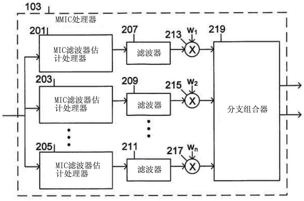
Fig. 2 is a block diagram of the MMIC processor 103 of fig. 1 in accordance with an embodiment of the disclosure.
Referring to fig. 2, the mmic processor 103 includes: a plurality of MIC filter estimation processors 201, 203, and 205; a plurality of filters 207, 209 and 211 corresponding to the plurality of MIC filter estimation processors 201, 203 and 205; a plurality of multipliers 213, 215, and 217 corresponding to the plurality of filters 207, 209, and 211; and a branch combiner 219. Fig. 2 shows: three of the multiple MIC filter estimation processors 201, 203, and 205; three of a plurality of filters 207, 209 and 211; and three of a plurality of multipliers 213, 215, and 217. However, the present disclosure is not limited to the use of three of each such component, and any number of each such component may be used.
Each of the MIC filter estimation processors 201, 203, and 205 or virtual channel is called a branch, and by selecting a different equalizer delay k for each branch0Is formulated. Each of the MIC filter estimation processors 201, 203, and 205 or virtual channel includes: an input connected to the output of the derotation processor 101 for outputting a residual channel h for a respective branchiAnd estimated filter piTo output of (c).
Each of the plurality of filters 207, 209, and 211 includes: an input connected to an output of one of the MIC filter estimation processors 201, 203, and 205, and an output.
Each of the plurality of multipliers 213, 215, and 217 includes: a first input coupled to an output of one of the plurality of filters 207, 209 and 211 for receiving a weight w corresponding to one of the plurality of MIC filter estimation processors 201, 203 and 2051,w2,…, wnWherein each multiplier of the plurality of multipliers 213, 215 and 217 is connected to the plurality of MIC filter estimation processors 201, 203 and 205 via a plurality of filters 207, 209 and 211.
The branch combiner 219 includes: multiple inputs connected to the outputs of multiple multipliers 213, 215 and 217 for providing a combined residual channel HresAnd a second output for providing a projected output y.
Fig. 3 is a flow diagram of a method of SAIC enhancement in a GSM UE receiver according to an embodiment of the present disclosure.
Referring to fig. 3, at 301, a PSK signal is received.
At 303, the received PSK signal is derotated by a derotation processor.
The derotated PSK signal is processed by an MMIC processor to produce a combined residual channel and projected output of the derotated PSK signal at 305.
The combined residual channel and filtered output is processed by the phase-rotated MLSE processor to produce hard and soft decision outputs 307.
Fig. 4 is a flow diagram of a method of the MMIC processor 103 of fig. 1 in accordance with an embodiment of the present disclosure.
Referring to fig. 4, at 401, the mmic processor 103 receives a derotated signal.
At 403, the derotated signal is processed by multiple MIC filter estimation processors (e.g., MIC filter estimation processors 201, 203, and 205 of FIG. 2) or branches, where each branch is processed by selecting a different equalizer delay k for each branch0Is formulated to output a valid channel h for the corresponding branchres,iAnd filters p estimated for the respective branch outputsi. For example, 3 branches may be formulated as represented by equations (10) through (12) above.
At 405, the effective channel h for each branch is filtered by a filterres,iAnd (6) filtering.
Each filtered effective channel is multiplied by a weight by a multiplier 407.
At 409, the weighted and filtered effective channels are combined to produce a projected output of the residual channel and the received signal.
Fig. 5 is a flow chart of a method of manufacturing a semiconductor device according to an embodiment of the present disclosure.
Referring to fig. 5, at 501, a semiconductor device is formed on a wafer or package having at least one semiconductor device, wherein the semiconductor device comprises: a plurality of MIC filter estimation processors, wherein each MIC filter estimation processor of the plurality of MIC filter estimation processors comprises a different equalizer offset k0And includes means for receiving the reverse rotationIs connected to the input of the first input of the IC processor and provides an effective channel hres,iAnd the estimated filter piA first output of (a); a plurality of filters, wherein each filter of the plurality of filters comprises an output and an input connected to a first output of one of the plurality of MIC filter estimation processors; a plurality of multipliers, wherein each of the plurality of multipliers comprises a first input connected to an output of one of the plurality of filters, a second input for receiving a weight, and an output; a branch combiner comprising a plurality of inputs connected to the outputs of the plurality of multipliers for providing a combined residual channel HresAnd a second output connected to the second output of the IC processor for providing a projected output y of the derotated signal.
At 503, the functionality of the semiconductor device is tested. The operation of testing the semiconductor device includes: semiconductor devices are tested using one or more electrical-to-optical converters, one or more optical splitters that split an optical signal into two or more optical signals, and one or more optical-to-electrical converters.
Fig. 6 is a flow diagram of constructing an integrated circuit according to an embodiment of the disclosure.
Referring to FIG. 6, at 601, initial layout data is constructed. For example, a mask layout is generated for a set of features of a layer of an integrated circuit, wherein the mask layout includes standard cell library macros for one or more circuit features, wherein the one or more circuit features include: a plurality of MIC filter estimation processors, wherein each MIC filter estimation processor of the plurality of MIC filter estimation processors comprises a different equalizer offset k0And comprises an input connected to a first input of the IC processor for receiving the derotated signal and providing an effective channel hres,iAnd the estimated filter piA first output of (a); a plurality of filters, wherein each filter of the plurality of filters comprises an output and a combinerAn input coupled to a first output of one of the plurality of MIC filter estimation processors; a plurality of multipliers, wherein each of the plurality of multipliers comprises a first input connected to an output of one of the plurality of filters, a second input for receiving a weight, and an output; a branch combiner comprising a plurality of inputs connected to the outputs of the plurality of multipliers for providing a combined residual channel HresAnd a second output connected to the second output of the IC processor for providing a projected output y of the derotated signal.
At 603, a design rule check is performed. For example, the method may check the relative positions of the macros after the mask layout is generated to comply with layout design rules.
At 605, the layout is adjusted. For example, upon detecting any macros that do not comply with the layout design rules, the method may modify the mask layout by modifying each non-compliant macro to comply with the layout design rules.
At 607, new layout data is generated. For example, the method may generate a mask based on the modified mask layout for the set of features having the layer of the integrated circuit. The integrated circuit layer according to the mask may then be fabricated.
Although specific embodiments of the present disclosure have been described in the detailed description thereof, various modifications may be made in the form of modifications to the disclosure without departing from the scope thereof. Accordingly, the scope of the present disclosure should be determined not only based on the described embodiments, but also based on the claims and their equivalents.
Claims (20)
1. An interference cancellation processor, comprising:
a plurality of single-tone interference cancellation filter estimation processors, wherein each of the plurality of single-tone interference cancellation filter estimation processors includes a different equalizer offset k0And includes means for receiving the derotated messageAn input for a signal connected to a first input of the interference cancellation processor, and providing an effective channel hres,iAnd estimated filter piA first output of (a);
a plurality of filters, wherein each filter of the plurality of filters comprises an output and an input connected to a first output of one of the plurality of single-tone interference cancellation filter estimation processors;
a plurality of multipliers, wherein each of the plurality of multipliers comprises a first input connected to an output of one of the plurality of filters, a second input for receiving a weight, and an output;
a branch combiner comprising a plurality of inputs connected to the outputs of the plurality of multipliers for providing a combined residual channel HresAnd a second output connected to the second output of the interference cancellation processor for providing a projected output y of the derotated signal.
2. The interference cancellation processor of claim 1, further comprising: a derotation processor configured to derotate a received signal, wherein the derotation processor comprises an input for receiving a signal and an output connected to the input of the interference cancellation processor.
3. The interference cancellation processor of claim 1, further comprising: a phase rotated maximum likelihood sequence estimation processor, wherein the phase rotated maximum likelihood sequence estimation processor comprises: a first input connected to a first output of the interference cancellation processor, a second input connected to a second output of the interference cancellation processor, a first input for providing a combined residual channel HresAnd a first output for hard decision of the projection output y, and a method for providing a combined residual channel HresAnd a second output projecting the soft decisions of output y.
4. The interference cancellation processor of claim 2, wherein the received signal is phase shift keying modulated, wherein the received signal includes gaussian minimum shift keying modulated interference.
5. The interference cancellation processor of claim 2, wherein the derotation processor is further configured to derotate a phase of the received signal
Wherein symbols are transmitted efficientlyThrough a processRotating, training symbol portions a [ t ]]Is a binary phase shift keyed signal, even for 8 phase shift keying,is due to continuityThe complex signal formed by the rotation of the optical fiber,is the received signal before phase derotation, L is a number of channel taps minus 1,is the channel of the user and is,is the channel of the interfering user(s),is noise and other interference, r [ t ]]Is the received signal after the de-rotation,is the equivalent transmission signal after phase derotation, hl]Is the equivalent channel of the user after phase derotation, g m]Is the equivalent channel of the interfering user after phase derotation, w t]Is the noise and other disturbances after phase derotation, b t-m]Is to be subjected to gaussian minimum shift keying modulated interference signals,
6. the interference cancellation processor of claim 1, wherein each of the plurality of single-tone interference cancellation filter estimation processors is configured to estimate the interference by multiplying p by piAnd hres,iIs determined asTo perform temporal interference whitening, wherein k is the time interference whitening0Is the equalizer delay, hresHas a length of 2 (Q)d+ 1), p has a length M (Q)p+ 1), where TS is the training sequence, T and T are integers, r [ T ]]Is the received signal after derotation, training symbol part a t]Is a binary phase shift keyed signal even for 8 phase shift keying, QdIs an integer for determining the channel length, M = 2x number of antennas x oversampling rate, QpThe number of consecutive time samples for chipx 1.
7. The interference cancellation processor of claim 1, wherein each of the plurality of single-tone interference cancellation filter estimation processors is configured to estimate the interference by selecting a bx B interference whitening matrixTo perform spatial interference whitening, wherein ReeIs estimated by Training Symbols (TS) as follows:
8. The interference cancellation processor of claim 3, wherein the phase-rotated maximum likelihood sequence estimation processor is configured to process the burst in two parts by: the left part of the burst is processed from the middle of the burst to the left of the burst from the training symbols and the right part of the burst is processed from the middle of the burst to the right of the burst from the training symbols.
9. The interference cancellation processor of claim 3 wherein the phase rotated maximum likelihood sequence estimation processor is configured to estimate the phase by pairingSolving to determine a maximum likelihood sequence estimate, wherein the residual e [ t ]]Is independent equal distribution (i.i.d.) additive white gaussian noise processing, t and l are integers,a[t]is a binary phase shift keyed signal even for 8 phase shift keying, QdIs an integer used to determine the length of the channel,andrespectively, for the real part of the complex signal and the imaginary part of the complex signal.
10. A method of combining channels of derotated signals by an interference cancellation processor, comprising:
generating an effective channel h by each of a plurality of single-tone interference cancellation filter estimation processorsres,iAnd estimated filter piWherein each of the plurality of single-tone interference cancellation filter estimation processors comprises a different equalizer offset k0And comprises an input connected to a first input of the interference cancellation processor for receiving the derotated signal;
estimating a generated effective channel h of each of the plurality of single-tone interference cancellation filter estimation processors through a plurality of filtersres,iFiltering is carried out;
filtering the effective channel h of the plurality of filters by a plurality of multipliersres,iEach multiplied by one of a plurality of weights;
generating a combined residual channel H by a finger combinerresAnd the projection output y of the derotated signal.
11. The method of claim 10, further comprising: derotation of the received signal by a derotation processor, wherein the derotation processor comprises an input for receiving the signal and an output connected to a first input of an interference cancellation processor.
12. The method of claim 10, further comprising: generation of a combined residual channel H by a phase-rotated maximum likelihood sequence estimation processorresHard decision of the sum projection output y and combined residual channel HresAnd a soft decision of the projection output y.
13. The method of claim 11, wherein the received signal is phase shift keying modulated, wherein the received signal includes gaussian minimum shift keying modulated interference.
14. The method of claim 11, wherein derotating the received signal by a derotation processor comprises derotating the phase of the received signal
Wherein symbols are transmitted efficientlyThroughRotating, training symbol portions a [ t ]]Is a binary phase shift keyed signal, even for 8 phase shift keying,is due to continuityThe complex signal formed by the rotation of the optical fiber,is the received signal before phase derotation, L is a number of channel taps minus 1,is the channel of the user and is,is the channel of the interfering user(s),is noise and other interference, r [ t ]]Is the received signal after the de-rotation,is the equivalent transmission signal after phase derotation, hl]Is the equivalent channel of the user after phase derotation, g m]Is the equivalent channel of the interfering user after phase derotation, w t]Is the noise and other interference after phase derotation, b [ t-m ]]Is to be subjected to gaussian minimum shift keying modulated interference signals,
15. the method of claim 10, further comprising: estimating, by each of the plurality of single-tone interference cancellation filter estimation processors, a signal by multiplying piAnd hres,iIs determined asTo perform temporal interference whitening, wherein k is the time interference whitening0Is the equalizer delay, hresHas a length of 2 (Q)d+ 1), p has a length M (Q)p+ 1), where TS is the training sequence, T and T are integers, r [ T ]]Is the received signal after derotation, training symbol part a t]Is a binary phase shift keyed signal even for 8 phase shift keying, QdIs an integer for determining the channel length, M = 2x number of antennas x oversampling rate, QpThe number of consecutive time samples for chipx 1.
16. The method of claim 10, further comprising: selecting a BxB interference whitening matrix by each of the plurality of single-tone interference cancellation filter estimation processorsTo perform spatial interference whitening, wherein ReeIs estimated by Training Symbols (TS) as follows:
17. The method of claim 12, further comprising: processing, by the phase-rotated maximum likelihood sequence estimation processor, the burst in two parts by: the left part of the burst is processed from the middle of the burst to the left of the burst from the training symbols and the right part of the burst is processed from the middle of the burst to the right of the burst from the training symbols.
18. The method of claim 12, further comprising: by the maximum likelihood sequence estimation processor of the phase rotationSolving to determine a maximum likelihood sequence estimate, wherein the residual e [ t ]]Is independent equal distribution (i.i.d.) additive white gaussian noise processing, t and l are integers,a[t]is a binary phase shift keyed signal even for 8 phase shift keying, QdIs an integer number used to determine the length of the channel,andrespectively, for the real part of the complex signal and the imaginary part of the complex signal.
19. A method of manufacturing a semiconductor device, comprising:
forming the semiconductor device as part of a wafer or package, wherein the semiconductor device comprises:
a plurality of single-tone interference cancellation filter estimation processors, wherein each single-tone interference cancellation filter estimation processor of the plurality of single-tone interference cancellation filter estimation processors comprises a different equalizer offset k0And comprises an input connected to a first input of the semiconductor device for receiving the derotated signal and providing an effective channel hres,iAnd estimated filter piA first output of (a);
a plurality of filters, wherein each filter of the plurality of filters comprises an output and an input connected to a first output of one of the plurality of single-tone interference cancellation filter estimation processors;
a plurality of multipliers, wherein each of the plurality of multipliers comprises a first input connected to an output of one of the plurality of filters, a second input for receiving a weight, and an output;
a branch combiner comprising a plurality of inputs connected to the outputs of the plurality of multipliers for providing a combined residual channel HresA first output connected to the first output of the semiconductor device and a second output connected to the second output of the semiconductor device for providing a projected output y of the derotated signal;
testing the semiconductor device, wherein the step of testing the semiconductor device is performed using at least one electrical-to-optical converter, at least one optical splitter that splits an optical signal into at least two optical signals, and at least one optical-to-electrical converter.
20. A method of constructing an integrated circuit, comprising:
generating a mask layout for a set of features of a layer of an integrated circuit, wherein the mask layout has standard cell library macros for:
a plurality of single-tone interference cancellation filter estimation processors, wherein each of the plurality of single-tone interference cancellation filter estimation processors includes a different equalizer offset k0And comprises an input connected to a first input of the integrated circuit for receiving the derotated signal and providing an effective channel hres,iAnd estimated filter piA first output of (a);
a plurality of filters, wherein each filter of the plurality of filters comprises an output and an input connected to a first output of one of the plurality of single-tone interference cancellation filter estimation processors;
a plurality of multipliers, wherein each of the plurality of multipliers comprises a first input connected to an output of one of the plurality of filters, a second input for receiving a weight, and an output;
a branch combiner comprising a plurality of inputs connected to the outputs of the plurality of multipliers for providing a combined residual channel HresA first output connected to a first output of the integrated circuit, and a second output connected to a second output of the integrated circuit for providing a projected output y of the derotated signal;
during the generation of the mask layout, ignoring the relative positions of the macros to comply with layout design rules;
after ignoring the relative positions of the macros, monitoring the relative positions of the macros to comply with layout design rules;
when a macro that does not comply with the layout design rule is detected, generating an adjusted mask layout by adjusting the non-compliant macro to comply with the layout design rule;
generating a mask according to the adjusted layout having the set of features for the layer of the integrated circuit;
an integrated circuit layer is fabricated according to the mask.
Applications Claiming Priority (4)
Application Number | Priority Date | Filing Date | Title |
---|---|---|---|
US201662411336P | 2016-10-21 | 2016-10-21 | |
US62/411,336 | 2016-10-21 | ||
US15/381,970 | 2016-12-16 | ||
US15/381,970 US9866411B1 (en) | 2016-10-21 | 2016-12-16 | Apparatus and method for single antenna interference cancellation (SAIC) enhancement |
Publications (2)
Publication Number | Publication Date |
---|---|
CN107979552A CN107979552A (en) | 2018-05-01 |
CN107979552B true CN107979552B (en) | 2022-11-01 |
Family
ID=61865891
Family Applications (1)
Application Number | Title | Priority Date | Filing Date |
---|---|---|---|
CN201710702781.2A Active CN107979552B (en) | 2016-10-21 | 2017-08-16 | Apparatus and method for Single Antenna Interference Cancellation (SAIC) enhancement |
Country Status (3)
Country | Link |
---|---|
KR (1) | KR102213716B1 (en) |
CN (1) | CN107979552B (en) |
DE (1) | DE102017112074A1 (en) |
Families Citing this family (1)
Publication number | Priority date | Publication date | Assignee | Title |
---|---|---|---|---|
CN110162854B (en) * | 2019-05-09 | 2023-05-26 | 重庆大学 | High-speed self-adaptive decision feedback equalizer |
Citations (2)
Publication number | Priority date | Publication date | Assignee | Title |
---|---|---|---|---|
CN1961518A (en) * | 2004-04-12 | 2007-05-09 | 诺基亚公司 | I/Q MIMO detection for single antenna interference cancellation |
CN101427506A (en) * | 2006-04-17 | 2009-05-06 | 高通股份有限公司 | Noise estimation for wireless communication |
Family Cites Families (5)
Publication number | Priority date | Publication date | Assignee | Title |
---|---|---|---|---|
US7565111B2 (en) * | 2004-02-26 | 2009-07-21 | Texas Instruments Incorporated | Single-antenna interference cancellation receiver in time slot communication system |
CN100518153C (en) * | 2005-03-01 | 2009-07-22 | 美国博通公司 | Method and device for carrying out balanced treatment for RF pulse |
US7539272B2 (en) * | 2005-11-30 | 2009-05-26 | Freescale Semiconductor, Inc. | Frequency error estimation and correction in a SAIC linear equalizer |
CN103051573B (en) * | 2012-12-12 | 2016-07-06 | 锐迪科科技有限公司 | Gsm system disturbs signal cancellation module and its implementation |
CN104683282B (en) * | 2015-02-16 | 2018-03-30 | 深圳市中兴微电子技术有限公司 | A kind of interference rejection combining method and device for supporting transmitting diversity |
-
2017
- 2017-03-30 KR KR1020170040427A patent/KR102213716B1/en active IP Right Grant
- 2017-06-01 DE DE102017112074.2A patent/DE102017112074A1/en active Pending
- 2017-08-16 CN CN201710702781.2A patent/CN107979552B/en active Active
Patent Citations (2)
Publication number | Priority date | Publication date | Assignee | Title |
---|---|---|---|---|
CN1961518A (en) * | 2004-04-12 | 2007-05-09 | 诺基亚公司 | I/Q MIMO detection for single antenna interference cancellation |
CN101427506A (en) * | 2006-04-17 | 2009-05-06 | 高通股份有限公司 | Noise estimation for wireless communication |
Also Published As
Publication number | Publication date |
---|---|
DE102017112074A1 (en) | 2018-04-26 |
CN107979552A (en) | 2018-05-01 |
KR102213716B1 (en) | 2021-02-09 |
DE102017112074A9 (en) | 2018-08-16 |
KR20180044175A (en) | 2018-05-02 |
Similar Documents
Publication | Publication Date | Title |
---|---|---|
US9473332B2 (en) | Methods and devices for communications systems using multiplied rate transmission | |
US7567635B2 (en) | Single antenna interference suppression in a wireless receiver | |
US6944245B2 (en) | Multi-pass interference reduction in a GSM communication system | |
JP5053378B2 (en) | Equalization structure and equalization method | |
TWI422167B (en) | Interference cancellation receiver and method | |
EP3264701B1 (en) | Frequency shift keying (fsk) demodulators | |
JP2013504261A (en) | Hardware simplification of SIC-MIMO decoding by using a single hardware element with channel and noise adaptation for the deinterfered stream | |
WO2008022170A2 (en) | Blind interference mitigation in a digital receiver | |
JP2008532354A (en) | Wireless communication apparatus and associated method for providing improved block equalization | |
KR20110014644A (en) | Spread-spectrum coding of data blocks using repetition | |
Modenini et al. | How to significantly improve the spectral efficiency of linear modulations through time-frequency packing and advanced processing | |
JP5053377B2 (en) | Equalization structure and equalization method | |
US7302233B2 (en) | Multiuser detection for wireless communications systems in the presence of interference | |
WO2007015143A2 (en) | Method, apparatus and computer program product providing widely linear interference cancellation for multi-carrier systems | |
JP2020174290A (en) | Wireless communication system, wireless communication method, transmission station device, and reception station device | |
CN107979552B (en) | Apparatus and method for Single Antenna Interference Cancellation (SAIC) enhancement | |
US9866411B1 (en) | Apparatus and method for single antenna interference cancellation (SAIC) enhancement | |
EP2680520B1 (en) | Method and apparatus for efficient MIMO reception with reduced complexity | |
Ju et al. | Achievable-rate-enhancing self-interference cancellation for full-duplex communications | |
WO2020085253A1 (en) | Wireless communication system, wireless communication method, transmitting station device, and receiving station device | |
Mattera et al. | MMSE WL equalizer in presence of receiver IQ imbalance | |
Gerstacker et al. | GSM/EDGE: A mobile communications system determined to stay | |
JP5047289B2 (en) | Equalization structure and equalization method | |
JP2020141174A (en) | Wireless communication system, wireless communication method, transmission station device, and reception station device | |
US10057094B2 (en) | Apparatus and method for single antenna interference cancellation (SAIC) enhancement |
Legal Events
Date | Code | Title | Description |
---|---|---|---|
PB01 | Publication | ||
SE01 | Entry into force of request for substantive examination | ||
GR01 | Patent grant | ||
GR01 | Patent grant |