CN107911096B - Chip with four filters operating with surface acoustic waves - Google Patents
Chip with four filters operating with surface acoustic waves Download PDFInfo
- Publication number
- CN107911096B CN107911096B CN201711281134.5A CN201711281134A CN107911096B CN 107911096 B CN107911096 B CN 107911096B CN 201711281134 A CN201711281134 A CN 201711281134A CN 107911096 B CN107911096 B CN 107911096B
- Authority
- CN
- China
- Prior art keywords
- filters
- chip
- ports
- output
- input
- Prior art date
- Legal status (The legal status is an assumption and is not a legal conclusion. Google has not performed a legal analysis and makes no representation as to the accuracy of the status listed.)
- Active
Links
- 238000010897 surface acoustic wave method Methods 0.000 title claims abstract description 27
- 239000000203 mixture Substances 0.000 claims description 3
- 101001128814 Pandinus imperator Pandinin-1 Proteins 0.000 claims description 2
- 101000927335 Pithecopus azureus Dermaseptin-H4 Proteins 0.000 claims description 2
- 238000000926 separation method Methods 0.000 claims description 2
- 238000003780 insertion Methods 0.000 description 9
- 230000037431 insertion Effects 0.000 description 9
- 239000000758 substrate Substances 0.000 description 6
- 230000008878 coupling Effects 0.000 description 4
- 238000010168 coupling process Methods 0.000 description 4
- 238000005859 coupling reaction Methods 0.000 description 4
- RYGMFSIKBFXOCR-UHFFFAOYSA-N Copper Chemical compound [Cu] RYGMFSIKBFXOCR-UHFFFAOYSA-N 0.000 description 3
- 229910052802 copper Inorganic materials 0.000 description 3
- 239000010949 copper Substances 0.000 description 3
- 239000011159 matrix material Substances 0.000 description 3
- 101000927339 Pithecopus azureus Dermaseptin-H3 Proteins 0.000 description 2
- 101000927330 Pithecopus azureus Dermaseptin-H6 Proteins 0.000 description 2
- 230000005540 biological transmission Effects 0.000 description 2
- 230000009977 dual effect Effects 0.000 description 2
- 230000002349 favourable effect Effects 0.000 description 2
- WSMQKESQZFQMFW-UHFFFAOYSA-N 5-methyl-pyrazole-3-carboxylic acid Chemical compound CC1=CC(C(O)=O)=NN1 WSMQKESQZFQMFW-UHFFFAOYSA-N 0.000 description 1
- 101001024685 Pandinus imperator Pandinin-2 Proteins 0.000 description 1
- 101000968091 Pithecopus azureus Dermaseptin-H2 Proteins 0.000 description 1
- 238000010586 diagram Methods 0.000 description 1
- GQYHUHYESMUTHG-UHFFFAOYSA-N lithium niobate Chemical compound [Li+].[O-][Nb](=O)=O GQYHUHYESMUTHG-UHFFFAOYSA-N 0.000 description 1
- 239000000463 material Substances 0.000 description 1
- 239000010453 quartz Substances 0.000 description 1
- VYPSYNLAJGMNEJ-UHFFFAOYSA-N silicon dioxide Inorganic materials O=[Si]=O VYPSYNLAJGMNEJ-UHFFFAOYSA-N 0.000 description 1
- 239000007787 solid Substances 0.000 description 1
Images


Classifications
-
- H—ELECTRICITY
- H03—ELECTRONIC CIRCUITRY
- H03H—IMPEDANCE NETWORKS, e.g. RESONANT CIRCUITS; RESONATORS
- H03H9/00—Networks comprising electromechanical or electro-acoustic elements; Electromechanical resonators
- H03H9/46—Filters
- H03H9/64—Filters using surface acoustic waves
- H03H9/6423—Means for obtaining a particular transfer characteristic
- H03H9/6433—Coupled resonator filters
- H03H9/6436—Coupled resonator filters having one acoustic track only
-
- H—ELECTRICITY
- H03—ELECTRONIC CIRCUITRY
- H03H—IMPEDANCE NETWORKS, e.g. RESONANT CIRCUITS; RESONATORS
- H03H9/00—Networks comprising electromechanical or electro-acoustic elements; Electromechanical resonators
- H03H9/70—Multiple-port networks for connecting several sources or loads, working on different frequencies or frequency bands, to a common load or source
- H03H9/72—Networks using surface acoustic waves
-
- H—ELECTRICITY
- H03—ELECTRONIC CIRCUITRY
- H03H—IMPEDANCE NETWORKS, e.g. RESONANT CIRCUITS; RESONATORS
- H03H9/00—Networks comprising electromechanical or electro-acoustic elements; Electromechanical resonators
- H03H9/0023—Networks for transforming balanced signals into unbalanced signals and vice versa, e.g. baluns, or networks having balanced input and output
- H03H9/0028—Networks for transforming balanced signals into unbalanced signals and vice versa, e.g. baluns, or networks having balanced input and output using surface acoustic wave devices
- H03H9/0033—Networks for transforming balanced signals into unbalanced signals and vice versa, e.g. baluns, or networks having balanced input and output using surface acoustic wave devices having one acoustic track only
- H03H9/0038—Networks for transforming balanced signals into unbalanced signals and vice versa, e.g. baluns, or networks having balanced input and output using surface acoustic wave devices having one acoustic track only the balanced terminals being on the same side of the track
-
- H—ELECTRICITY
- H03—ELECTRONIC CIRCUITRY
- H03H—IMPEDANCE NETWORKS, e.g. RESONANT CIRCUITS; RESONATORS
- H03H9/00—Networks comprising electromechanical or electro-acoustic elements; Electromechanical resonators
- H03H9/02—Details
- H03H9/05—Holders or supports
-
- H—ELECTRICITY
- H03—ELECTRONIC CIRCUITRY
- H03H—IMPEDANCE NETWORKS, e.g. RESONANT CIRCUITS; RESONATORS
- H03H9/00—Networks comprising electromechanical or electro-acoustic elements; Electromechanical resonators
- H03H9/02—Details
- H03H9/05—Holders or supports
- H03H9/0538—Constructional combinations of supports or holders with electromechanical or other electronic elements
- H03H9/0566—Constructional combinations of supports or holders with electromechanical or other electronic elements for duplexers
- H03H9/0576—Constructional combinations of supports or holders with electromechanical or other electronic elements for duplexers including surface acoustic wave [SAW] devices
-
- H—ELECTRICITY
- H03—ELECTRONIC CIRCUITRY
- H03H—IMPEDANCE NETWORKS, e.g. RESONANT CIRCUITS; RESONATORS
- H03H9/00—Networks comprising electromechanical or electro-acoustic elements; Electromechanical resonators
- H03H9/46—Filters
- H03H9/64—Filters using surface acoustic waves
-
- H—ELECTRICITY
- H03—ELECTRONIC CIRCUITRY
- H03H—IMPEDANCE NETWORKS, e.g. RESONANT CIRCUITS; RESONATORS
- H03H9/00—Networks comprising electromechanical or electro-acoustic elements; Electromechanical resonators
- H03H9/70—Multiple-port networks for connecting several sources or loads, working on different frequencies or frequency bands, to a common load or source
- H03H9/72—Networks using surface acoustic waves
- H03H9/725—Duplexers
Landscapes
- Physics & Mathematics (AREA)
- Acoustics & Sound (AREA)
- Surface Acoustic Wave Elements And Circuit Networks Thereof (AREA)
Abstract
The invention relates to a chip having four filters operating with surface acoustic waves, the Chip (CH) having four filters operating with surface acoustic waves (F1, F2, F3, F4) and input ports and outputs (EP1, EP2, AP1, AP 2). Each filter (F1, F2, F3, F4) covers a different frequency band. Each of the input and output ports (EP1, EP2, AP1, AP2) is connected to one or two filters (F1, F2, F3, F4).
Description
The present application is a divisional application of an invention patent application having an application number of 201180053281.1, an application date of 2011-11-3, and an invention name of "a chip having four filters operating with surface acoustic waves".
Technical Field
The invention relates to a chip with four filters operating with surface acoustic waves.
Background
Such modules are known: the module has four SAW (surface acoustic wave) filters and also duplexers at its input and output ports, so that the four filters can be driven via two input ports and two output ports in each case.
Disclosure of Invention
The object of the invention is to simplify the known module and to optimize it with respect to cost and space requirements.
This object is achieved by a chip as described below and by a package as described below. Advantageous embodiments of the invention are found in the further description of the present application.
According to the invention, a chip is proposed, which has four filters operating with surface acoustic waves and input and output ports. Each covering a different frequency band. Each of the input and output ports is connected to one or two filters. The four filters are arranged on the chip as follows: such that two filters form a left column and the remaining two filters form a right column; two of the four filters, each from a column, are disposed opposite each other; and two oppositely positioned filters each connected to an output port disposed between two filters opposite to each other, the two input ports including a first input port and a second input port, each of the two input ports being connected to one of the four filters connected to the first of the two output ports and the other of the four filters connected to the second of the two output ports; and the two filters are coupled to a first of the two input ports, the remaining two filters are coupled to a second of the two input ports, one of the two filters and one of the remaining two filters are used for one band from a low band, respectively, and one of the two filters and one of the remaining two filters are used for one band from a high band, respectively; and each of the four filters is a receive filter of a receive circuit. The present invention also provides a package comprising: four filters operating with surface acoustic waves, the four filters being arranged as follows: such that two of the four filters form a left column and the remaining two filters form a right column, wherein two of the four filters, each from a column, are disposed opposite each other, the filters being disposed on two or more chips; each of the four filters covers a different frequency band; each of the four filters is a reception filter of the reception circuit, and each of the two oppositely positioned filters is connected to an output port provided between the two filters opposed to each other; the chip is provided with two input ports and two output ports, wherein the two input ports comprise a first input port and a second input port, and the two output ports comprise a first output port and a second output port; each of the two input ports is connected to one of the four filters connected to the first output port and the other of the four filters connected to the second output port; and the two filters are coupled to a first one of the two input ports, the remaining two filters are coupled to a second one of the two input ports, one of the two filters and one of the remaining two filters are used for one band from a low band, respectively, and one of the two filters and one of the remaining two filters are used for one band from a high band, respectively.
Furthermore, a particularly advantageous arrangement of the filters on the chip can be selected. For this purpose, four filters are arranged on the chip as follows: so that two filters form a left column and the remaining two filters form a right column, and the two filters, each from a different column, are disposed opposite each other.
The input and/or output ports can be connected to both filters. In this case, they form a duplexer.
If the chip has two input ports which are connected in each case to two filters each forming a duplexer, the two filters of the left column can be connected to the first input port and the two filters of the right column can be connected to the second input port.
If the chip has two output ports which are connected in each case to two filters which each form a duplexer, the two oppositely situated filters can each be connected to an output port which is arranged between the two filters lying opposite one another.
If the duplexer functionality of four filters operating with surface acoustic waves is integrated in one chip, it is possible in this way to achieve distinct advantages with respect to space requirements.
Such a chip can be used in the transmitting and receiving circuits of a mobile phone. The remaining components of the transmit and receive circuitry can be simplified if the input and/or output ports of the chip are then provided as duplexers. For example, if the input ports of four filters are provided as duplexers, the assembly has only two input ports instead of four. The input port is typically connected separately to the antenna, optionally via a switch. Arranging the chip with only two input ports makes it possible to use less complex and correspondingly more advantageous switches for discriminating the received frequency bands. On the output side, the number of signal lines between the chip and the receiving circuit is reduced by half due to the duplex output port.
Each of the two input ports is advantageously connected to a filter connected to the first output port and to a filter connected to the second output port.
In the first embodiment of the present invention, four SAW filters are arranged in a row on a common chip substrate.
In the second embodiment, four filters are arranged in the form of a2 × 2 matrix on a chip. In this arrangement, two filters form a left column and the remaining two filters form a right column, the two filters of the left column being connected to the first input port and the two filters of the right column being connected to the second input port. The two filters, each from a different column, are in this case arranged opposite each other, and the two filters opposite each other are each connected to an output port arranged between the two filters opposite each other.
This second embodiment has some advantages compared to the first embodiment. On the one hand, crossing of signal lines on the chip can be avoided. Further, the arrangement of the filter according to the second embodiment makes it possible to constitute a chip whose ratio of length and width has more favorable characteristics. The chip according to the first embodiment has only a large length but on the other hand a small width. In the case of the chip according to the second embodiment, the ratio of the length to the width is close to one.
The aspect ratio of the second embodiment corresponds to the standard form used, for example, in the case of a 2-in-1 (2 in 1) filter chip. In the market, many dual band mobile phones are known, wherein 2-in-1 filter chips with two SAW filters for two different frequency bands are used. The chip according to the second embodiment of the invention has the same dimensions and thus the same aspect ratio as the known 2-in-1 filter chip. It is thus possible to replace the 2 in1 filter chip with the 4 in1 filter chip according to the invention without much expense and thus to upgrade a dual band mobile phone to form a quad band mobile phone. In contrast, if a 4-in-1 filter chip having a large length and a small width according to the first illustrative embodiment is used, a larger change is required in the design of the circuit board.
Since the dimensions of the second illustrative embodiment correspond to standard forms, existing tools can be used for production as well as for testing chips.
In addition, the second embodiment has better mechanical stability due to the varying length to width ratio. Since the chip according to the second embodiment has a length to width ratio close to unity, it is in particular less sensitive to deformations due to temperature fluctuations. In the chip according to the first illustrative elastic embodiment, the mechanical stress can rise. Since the absolute size has been reduced in length in the chip according to the second embodiment, the mechanical stress that can rise due to thermal deformation is reduced. The improved mechanical stability leads to better reliability and reduced failure probability.
The advantages of the chip according to the second embodiment are therefore a more compact layout, improved reliability and the possibility of using existing tools.
The frequency space can be divided into a high frequency band and a low frequency band. The definition of the high and low frequency bands depends on the standard used in each case and is initially completely arbitrary. One possible definition allocates frequencies below 1GHz to the low frequency band and frequencies above 1GHz to the high frequency band. In the following, this definition serves as a basis, without restricting the invention to this definition.
Two of the four SAW filters each cover a frequency band in the high frequency band, and the remaining two SAW filters each cover a frequency band in the low frequency band. In this case, the first input port can be connected to a filter covering a first frequency band in the high frequency band and a filter covering a first frequency band in the low frequency band. Accordingly, the second input port is connectable to a filter covering a second frequency band in the high frequency band and a filter covering a second frequency band in the low frequency band.
On the output side, the first output port is connectable to two filters covering two bands in the high frequency band, and the second output port is connectable to two filters covering two bands in the low frequency band.
The filter can cover, for example, four GSM bands. These can be GSM 850 and GSM 900 bands in the low band and GSM 1800 and GSM 1900 bands in the high band. However, the invention is not limited to filters for the GSM band. The invention can also comprise filters for frequency bands defined according to the UMTS standard, for example.
The output port can be balanced or single ended. The filter can be a ladder or DMS filter or a mixture of both.
The chip can also have matching elements which make it possible to match the frequency characteristics of the filters to one another. This is decisive, in particular, when the two filters form a duplexer. In this case, each filter should in each case reflect signals lying within the passband of the other filter.
For matching purposes, an inductance and a capacitance can be provided between the two filters on the chip. It is possible to realize this inductance and capacitance by means of a resonator. Furthermore, the input port can be connected to an external coil. In addition, other matching elements can be realized on the chip, for example by means of an inductance made of copper.
The chip substrate can be quartz, lithium niobate or lithium tantalate.
The invention also relates to a package with a chip according to the invention. Such a package preferably also presents one or more inductors, in particular copper coils, for improved diplexer separation. The inductance can be provided on a surface of the package or integrated into a substrate of the package.
The invention also relates to a package in which four filters operating with surface acoustic waves are provided in the second embodiment described above, each covering a different frequency band. In this arrangement, four filters are set as follows: so that two filters form the left column and the remaining two filters form the right column. The two filters from each column are each arranged opposite to each other.
The filters can be provided on two or more chips. The chips can include different substrate materials. The filters are preferably distributed over two chips. The filters forming the left column are arranged on a first chip and the filters forming the right column are arranged on a second chip. The two chips are positioned opposite each other.
Furthermore, each of the two chips can have one input port connected to both filters of the chip. The two chips form a duplexer. This arrangement corresponds to the illustrative embodiment described above, in which the two filters each form an input duplexer. However, in contrast to the illustrative embodiments described above, the four filters are now distributed over two separate chip substrates.
The package can have two output ports, and each of the output ports can be individually connected to one filter on each of the two chips. In this case, the two filters each form a duplexer, the first filter being provided on one chip, and the second filter being provided on the other chip.
Thus, the package according to the current claim 18 substantially corresponds to the chip according to the current claim 2, with only the filters being distributed over two or more chips.
Drawings
In the following, the invention will be explained in more detail with reference to illustrative embodiments and the associated drawings. The drawings illustrate various illustrative embodiments of the invention by way of graphical representations that are not solid scale.
Figure 1 shows a diagrammatic representation of a transmit and receive circuit.
FIG. 2 shows a graphical representation of a first illustrative embodiment of a chip.
FIG. 3 shows a graphical representation of a second illustrative embodiment of a chip.
Fig. 4 shows the insertion loss and the standing wave ratio of the first filter F1.
Fig. 5 shows the insertion loss and the standing wave ratio of the second filter F2.
Fig. 6 shows the insertion loss and the standing wave ratio of the third filter F3.
Fig. 7 shows the insertion loss and the standing wave ratio of the fourth filter F4.
Fig. 8 shows a package.
Fig. 9 illustrates an advantageous package.
FIG. 10 shows, in a diagrammatic representation, another variant of the second illustrative embodiment of a chip.
Detailed Description
Fig. 1 shows a diagrammatic representation of a transmitting and receiving circuit in a mobile telephone connecting an antenna 1 to an RF circuit 2. The transmit and receive circuit has four signal paths SP1, SP2, SP3, SP4, the upper two signal paths SP1, SP2 forming the receive circuit and the lower two signal paths SP3, SP4 forming the transmit circuit. The two signal paths SP1, SP2 of the receiving circuit are each connected to one input port EP1, EP2 of the chip CH.
The chip CH has four SAW filters F1, F2, F3, F4 and two input ports EP1, EP2 and two output ports AP1, AP 2. At the input ports EP1, EP2, the two filters are interconnected in each case to form a duplexer. Thus, each of the two input ports EP1, EP2 is in each case connected to two SAW filters F1, F3 and F2, F4, respectively. The output ports AP1, AP2 are also embodied as duplexers and are in each case cross-connected to two SAW filters F1, F2 and F3, F4, respectively. In addition, the output ports AP1, AP2 are balanced here, so that the chip has a total of four output terminals AP1a, AP1b, AP2a, AP2b, the two output terminals AP1a, AP1b and AP2a, AP2b forming in each case one output port AP1 and AP2, respectively.
The antenna 1 can optionally be connected via a switch S to one of the two signal paths SP1, SP2 of the receiving circuit, each of the two signal paths SP1, SP2 leading to one of the input ports EP1, EP2 of the chip. On the output side, the output ports AP1, AP2 of the chip are connected to two low noise amplifiers LNA1, LNA 2.
In addition, the antenna 1 can be connected to one of the two transmission paths SP3, SP4 of the transmission circuit via the switch S. Each of the transfer paths SP3, SP4 has preamplifiers VV1 and VV2, main amplifiers HV1 and HV2, and low pass amplifiers LPF1 and LPF 2.
Fig. 2 shows an arrangement of SAW filters F1, F2, F3, F4 in a chip CH according to the present invention according to the first illustrative embodiment. Two input ports EP1 and EP2 are located on the input side. The first input port EP1 is connected to filters F1 and F3. The second input port EP2 is connected to filters F2 and F4. The filters F1 and F2 are filters for a frequency band in a high frequency band, and the filters F3 and F4 are filters for a frequency band in a low frequency band. These can be, for example, frequency bands defined according to the GSM standard. Filter F1 is designed for the 1960MHz GSM band and filter F2 is designed for the 1842.5MHz GSM band. Accordingly, both bands are in the high band. The filters F3(942.5MHz) and F4(881.5MHz) cover the frequency band according to the GSM standard and are located in the low frequency band.
The invention is however by no means limited to frequency bands according to the GSM standard. The four filters F1, F2, F3, F4 can also be designed, for example, for four frequency bands according to the UMTS standard.
According to the first illustrative embodiment shown in fig. 2, the four filters F1-F4 are DMS structures. In this context, each of the four filters F1-F4 is composed of a combination of two filter structures FS1a, DMS1b, FS2a, DS2b, FS3a, DMS3b, FS4a, DMS4b, one of which can be a DMS structure.
The configuration of such a filter consisting of two filter structures is discussed by means of the first filter F1. The other filters F2, F3, F4 can have similar filter structures.
The first filter structure FS1a of the first filter F1 is a series resonator. The output of the first filter structure FS1a is here connected simultaneously via three parallel signal lines SL1, SL2, SL3 to the building units of the second filter structure DMS1 b.
The second filter structure DMS1b is a DMS structure and has three coupled converters and two output converters. The signal lines SL1, SL2, SL3 connected to the output of the first filter structure FS1 are in each case connected to a coupling converter. The outputs AO1, AO2 of the two output converters of the DMS structure DMS1b are in each case connected to one output port AP1, AP2 of the chip CH. In this arrangement, the first output ports AP1 are each connected to one of the filters F1 and F2. The first output port AP1 has two output terminals AP1a, AP1b, and is set to be balanced. A second output port AP2, which also has two output terminals AP2a, AP2b and is set to be balanced, is connected to the filters F3 and F4.
The arrangement shown here represents a simplification of the actual filter structure. A filter for the GSM 1900MHz band can be formed by a series circuit of resonators and a DMS filter structure having six IDTs. The resonator and DMS filter represent the first and second filter structures, respectively. The filter for the GSM 1800MHz band can have series and parallel resonators as the first filter structure and a DMS filter structure with six IDTs as the second filter structure. The filter for the GSM 850 and 950MHz bands can have a DMS structure with three IDTs on the output side as the second filter structure and series and parallel resonators as the first filter structure. Furthermore, further resonators can be used at the input between the duplex filters in order to provide an improved matching.
If two filters form a duplexer, the frequency characteristics of the two filters must be matched to each other by matching elements. Signals located within the pass band of one filter should be reflected by the other filter. On the input side of the chip, further elements can thus be provided which provide a corresponding matching of the filter.
For example, an external coil connected to one of the input ports EP1, EP2 may be used. Further, an inductance and a capacitance can be provided between the two filters forming the duplexer. This combination of inductance and capacitance can also be achieved by the resonator. A copper coil mounted on the chip CH can be used as a further matching element.
The present invention is in no way limited to the arrangement of SAW filters F1-F4 shown herein. In addition to the DMS structure, the filters F1-F4 can be provided as ladder filters, or a mixture of ladder and DMS filters is conceivable. In these contexts, a ladder structure is cascaded with a DMS structure.
The input ports EP1 and EP2 are in each case connected to filters F1 and F2, respectively, for the frequency bands in the high frequency band and to filters F1 and F4, respectively, for the frequency bands in the low frequency band, while one output port AP1 is connected to filters F1, F2 for one frequency band, respectively, from the high frequency band, and the other output port AP2 is connected to filters F3, F4 for one frequency band, respectively, from the low frequency band. Accordingly, crossing of signal lines on the input side or the output side cannot be avoided in the chip CH according to this first embodiment.
Fig. 3 shows a second illustrative embodiment of a chip CH according to the invention. The second illustrative embodiment differs from the illustrative embodiment shown in fig. 2 by the arrangement of SAW filters F1-F4 on the chip substrate. The four filters F1-F4 are now arranged in the form of a2 x 2 matrix having two rows and two columns. Filters F1 and F2 form a first row, filters F3 and F4 form a second row, and filters F1 and F3 and filters F2 and F4 form in each case one column respectively. Filters F1 and F3 are disposed on the left side of the chip CH, and are connected to the first input port EP 1. Filters F2 and F4 are disposed on the right side and are connected to the second input port EP 2.
The terminals AP1a, AP1b, AP2a, AP2b of the output ports AP1, AP2 are each disposed between filters F1-F4. The terminals AP1a, AP1b of the first output port AP1 are disposed between the filter F1 and the filter F2. The terminals AP2a, AP2b of the second output port AP2 are disposed between the filters F3 and F4, and are connected to the two filters F3, F4. Here, the output ports AP1, AP2 are in each case set to be balanced.
The arrangement of the filters F1-F4 according to the second illustrative embodiment presents several advantages compared to the arrangement shown in fig. 2. The chip CH is generally more compact, resulting in a more favorable ratio of length to width. This allows standard tools to be used for mounting and testing the chip CH. Furthermore, no crossing of signal lines is required on the input side. There is also no signal crossing on the output side.
Thus, signal crossing is avoided at the chip level. Line crossings may occur at the output side only when the chip is connected to the pads of the package.
The invention is not limited to the embodiments of the chip shown here. Thus, for example, the acoustic tracks (acoustic tracks) of each individual SAW filter F1-F4 can be rotated by 90 ° about their respective center point in the arrangement according to FIG. 3. Correspondingly, the outputs of the SAW filters F1-F4 also rotate to different positions. In this case, a shorter signal path for connecting the output terminals AP1a/b and AP2a/b to the terminals of the package can be generated.
FIG. 10 shows a graphical representation of one possible embodiment of the second illustrative embodiment. This representation is therefore described in more detail, in particular the filter structure is more accurately decomposed.
Four SAW filters F1, F2, F3, and F4 are again arranged in a square on a chip. The filters F1-F4 form a2 × 2 matrix, respectively two filters F1 and F3 and F2 and F4, each arranged in a column. Further, filters F1 and F2 and filters F3 and F4 from different columns, respectively, are disposed opposite to each other.
Two input ports EP1 and EP2 are located on the input side. The first input port EP1 is connected to filters F1 and F3 forming a duplexer. The second input port EP2 is connected to filters F2 and F4. The filters F1 and F2 are filters for a frequency band in a high frequency band, and the filters F3 and F4 are filters for a frequency band in a low frequency band. These can be, for example, frequency bands defined according to the GSM standard. The filter F1 is for example designed for the GSM band of 1960MHz, the filter F2 is designed for the GSM band of 1842.5 MHz. Accordingly, both bands are located in the high band. The filters F3(942.5MHz) and F4(881.5MHz) cover the frequency band according to the GSM standard and are located in the low frequency band.
Each of the filters F1-F4 is composed of a plurality of filter structures. The filter F1 for the GSM band at 1900MHz has a DMS structure DMS1a connected in series with a second filter structure FS1 b. The first DMS structure DMS1a has two input converters and four coupled converters. The second filter structure FS1b has two resonators, in this case implemented as four-port resonators. The output of the second filter structure FS1b of the first filter F1 is connected to the output terminals AP1a, AP1b of the first output port AP 1. The first output port AP1 is balanced. The two signal paths for balanced operation are via two-port resonator FS1 b.
The second filter F2 for the GSM band of 1800MHz is disposed opposite to the first filter F1. The second filter has three filter structures DMS2a, FS2b and FS2 c. The first filter structure of the second filter F2 is the DMS structure DMS2a, and has a total of six IDTs, two input converters, and four coupling converters. The DMS structure DMS2a is connected in series with the second filter structure FS2 b. The second filter structure FS2b has two resonators, here again implemented as four-port resonators. A third filter structure FS2c, also having two resonators consisting of four-port resonators, is connected in parallel with the second filter structure FS2 b. The parallel two-port resonator FS2c is actually connected to ground and, on the input side, two balanced signals are connected to it. The output terminals AP1a, AP1b of the first output port AP1 are connected in series with the second filter structure FS2b and in parallel with the third filter structure FS2c of the second filter F2.
The third filter F3 for the GSM band of 942.5MHZ forms a duplexer together with the first filter F1. The third filter F3 has three resonators FS3a, FS3b, FS3c and DMS structure DMS3 d. The first resonator FS3a is directly connected to the first input port EP 1. The third resonator FS3c is connected in series with the first resonator FS3 a. In addition, the second resonator FS3b is connected in parallel to ground between the first and third resonators. The third resonator FS3c is connected to the DMS structure DMS3d via three parallel signal lines, DMS3d has three coupling converters and two output converters. The two outputs of the DMS structure DMS3d are in each case connected to one of the output terminals AP2a, AP2b of the second output port AP2, the second output port AP2 being balanced.
The fourth filter F4 for the GSM band of 850MHz is constituted similarly to the third filter F3. The fourth filter F4 also has three resonators FS4a, FS4b, FS4c and DMS structure DMS4d, the first resonator FS4a being directly connected to the second input port EP 2. The output of the first resonator FS4a is also connected to the third resonator FS4 c. The second resonator FS4b is connected in parallel to ground between the first and third resonators. The third resonator FS4c is connected to the DMS structure DMS3d via three parallel signal lines, DMS3d has three coupling converters and two output converters. The two outputs of the DMS structure DMS4d are in each case connected to one of the output terminals AP2a, AP2b of the second output port AP 2.
The present invention is in no way limited to the arrangement of filters F1-F4 shown in fig. 10 and the precise configuration of filters F1-F4 shown therein. Thus, within the scope of the invention are also possible: the chip has four input ports and four output ports, with each filter F1-F4 connected to exactly one input port and exactly one output port. Furthermore, the two filters may each be interconnected so as to form one duplexer only on the input side or only on the output side.
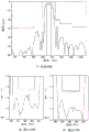
Fig. 4 shows the insertion loss and the standing wave ratio of the first filter F1. The first filter F1 is designed for the GSM band of 1960 MHz. The upper graph shows the insertion loss. Here it can be seen that there is a very fine insertion loss in the pass band between 1930 and 1990 MHz. In contrast, in the stop band, the insertion loss exceeds 35 dB.
In the two following figures, the standing wave ratio is shown. The left graph shows the standing wave ratio at the input side of the filter. This diagram shows that the reflected signal becomes very low in the pass band. The right graph shows the standing wave ratio at the output side. Here, too, only very fine signal components are reflected in the pass band.
Fig. 5 to 7 show the insertion loss and standing wave ratio of the input side and the output side of the filters F2, F3, and F4, respectively. The filter F2 is designed for the GSM band of 1842.5 MHz. The filter F3 is designed for the GSM low band at 942.5 MHz. The filter F4 is designed for the GSM low band of 881.5 MHz.
Fig. 8 shows a diagrammatic representation of a package PA with a chip CH according to the invention. The package PA has a rectangular basic shape with two long sides and two short sides, which in each case form an angle of 90 ° with the long sides.
The package PA also has eight pins Pin1-Pin8 via which it can be connected to a circuit board and other components. Four pins Pin1-Pin4 are provided on a first long side and four other pins Pin5-Pin8 are provided on an opposite second long side.
Pin1 is generally available for the first input port EP1 and Pin4 for the second input port EP 2. Furthermore, if the output ports AP1, AP2 are single ended, Pin5 and Pin8 are used to connect the two output ports AP1, AP 2. In the case of balanced output ports AP1, AP2, Pin5 and Pin6 are used for the first output port AP1 and Pin7 and Pin8 are used for the second output port AP 2.
Pin2 and Pin3 can be used as ground supply sources.
Fig. 9 shows a modified arrangement of the package PA. Additionally, this package PA has two further pins Pin9 and Pin10 arranged on a short side of the package and also two further pins Pin11 and Pin12 arranged on the opposite second short side.
Pin9-Pin12 are now used to connect the output ports AP1, AP 2. This configuration provides the following advantages: the output ports AP1, AP2 of the chip CH can be connected to the terminals Pin9-Pin12 of the package PA via short symmetrical signal lines.
Reference numerals
1-aerial
2-RF circuit
SP 1-first Signal Path
SP 2-second Signal Path
SP 3-third Signal Path
SP 4-fourth Signal Path
CH-chip
EP 1-first input port
EP 2-second input port
F1-first filter
F2-second Filter
F3-third Filter
F4-fourth Filter
AP 1-first output port
AP 2-second output port
AP1 a-first terminal of AP1
Second terminal of AP1 b-AP 1
First terminal of AP2 a-AP 2
Second terminal of AP2 b-AP 2
S-switch
LNA 1-first Low noise Amplifier
LNA 2-second Low noise Amplifier
VV 1-first preamplifier
VV 2-second preamplifier
HV 1-first main amplifier
HV 2-second main amplifier
LPF 1-first Low pass Filter
LPF 2-second Low pass Filter
FS1 a-F1 first filter structure
Second DMS Structure of DMS1 b-F1
FS2 a-F2 first filter structure
Second DMS Structure of DMS2 b-F2
FS3 a-F3 first filter structure
Second DMS Structure of DMS3 b-F3
FS4 a-F4 first filter structure
Second DMS Structure of DMS4 b-F4
SL 1-first signal line
SL 2-second signal line
SL 3-third signal line
First output of AO 1-DMS 1b
Second output of AO 2-DMS 1b
PA package
Pin 1-first Pin.
Claims (19)
1. A Chip (CH) has
Four filters (F1, F2, F3, F4) operating with surface acoustic waves, each of the four filters (F1, F2, F3, F4) covering a different frequency band, and each of the two input ports (EP1, EP2) and each of the two output ports (AP1, AP2) being connected to two filters of the four filters (F1, F2, F3, F4),
wherein:
the four filters (F1, F2, F3, F4) are arranged on the Chip (CH) as follows: so that two filters (F1, F3) form the left column and the remaining two filters (F2, F4) form the right column;
two of the four filters (F1, F2, F3, F4), each from a column, are disposed opposite to each other; and
two oppositely positioned filters (F1, F2, F3, F4) are each connected to an output port (AP1, AP2) arranged between two mutually opposite filters (F1, F2, F3, F4),
the two input ports include a first input port and a second input port, each of the two input ports being connected to one of the four filters connected to a first output port of the two output ports and another one of the four filters connected to a second output port of the two output ports; and
the two filters (F1, F3) are coupled to a first one of the two input ports (EP1, EP2), the remaining two filters (F2, F4) are coupled to a second one of the two input ports (EP1, EP2), one of the two filters (F3) and one of the remaining two filters (F4) are used for one band from the low band, respectively, and one of the two filters (F1) and one of the remaining two filters (F2) are used for one band from the high band, respectively; and
each of the four filters (F1, F2, F3, F4) is a reception filter of a reception circuit.
2. Chip (CH) according to claim 1,
wherein each of the two input ports (EP1, EP2) is connected to two of the four filters (F1, F2, F3, F4) forming a diplexer.
3. Chip (CH) according to claim 1,
wherein the two filters (F1, F3) of the left column are connected to the first input port (EP1) and the remaining two filters (F2, F4) of the right column are connected to said second input port (EP 2).
4. Chip (CH) according to one of the claims 1 to 3,
wherein the chip has two output ports (AP1, AP2), and each of the output ports (AP1, AP2) is connected to two of the four filters (F1, F2, F3, F4) each forming a duplexer.
5. Chip (CH) according to claim 4,
wherein the first output port (AP1) is connected to the two filters (F1, F2) covering the two of the high frequency bands, and the second output port (AP2) is connected to the two filters (F3, F4) covering the two of the low frequency bands.
6. Chip (CH) according to one of the claims 1 to 3,
further comprising elements for matching the frequency characteristics of the four filters (F1, F2, F3, F4).
7. Chip (CH) according to one of the claims 1 to 3,
wherein the output ports (AP1, AP2) are balanced.
8. Chip (CH) according to one of the claims 1 to 3,
wherein the output ports (AP1, AP2) are single ended.
9. Chip (CH) according to one of the claims 1 to 3,
wherein the four filters (F1, F2, F3, F4) are each designed as a ladder or DMS filter or as a mixture of the two filter types.
10. Chip (CH) according to one of the claims 1 to 3,
wherein one of the four filters (F1) has a DMS structure (DMS1a), which DMS structure (DMS1a) is connected to one of the two input ports (EP1) and is connected in series with a resonator (FS1b), and wherein the resonator (FS1b) is connected to an output port (AP 1).
11. Chip (CH) according to one of the claims 1 to 3,
wherein:
one of the four filters (F2) has a DMS structure (DMS2a) and two resonators (FS2b, FS2 c);
the DMS structure (DMS2a) is connected to one of the two input ports (EP2) and is connected in series with a first resonator (FS2 b);
a second resonator (FS2c) connected in parallel with the first resonator (FS2 b);
the second resonator (FS2c) is actually connected to ground; and
the first resonator (FS2b) is connected to an output port (AP 2).
12. Chip (CH) according to one of the claims 1 to 3,
wherein two of the filters (F3, F4) have three resonators (FS3a, FS3b, FS3c, FS4a, FS4b, FS4c) and DMS structure (DMS3d, DMS4d), respectively;
a first resonator (FS3a, FS4a) is connected to one of the two input ports (EP1, EP 2);
a third resonator (FS3c, FS4c) is connected in series with the first resonator (FS3a, FS4 a);
a second resonator (FS3b, FS4b) is connected in parallel to ground between the first and third resonators (FS3a, FS4a, FS3c, FS4 c);
-the third resonator (FS3c, FS4c) is interconnected in series with the DMS structure (DMS3d, DMS4 d); and
the DMS structure (DMS3d, DMS4d) is connected to the output ports (AP3, AP 4).
13. A Package (PA) with a Chip (CH) according to one of claims 1 to 3.
14. The Package (PA) of claim 13,
further comprising an inductance for improved diplexer separation.
15. The Package (PA) of claim 13,
wherein the underside of the package has a rectangular shape with two long sides and two short sides perpendicular to the long sides, pins (Pin1, Pin4) for connecting the two input ports (EP1, EP2) are arranged on one of the long sides, and pins (Pin5-Pin8, Pin9-Pin12) for connecting the output ports (AP1, AP2) are arranged on the other long side or on the two short sides.
16. A Package (PA) comprising:
four filters (F1, F2, F3, F4) operating with surface acoustic waves, said four filters (F1, F2, F3, F4) being arranged in the following way: such that two of the four filters (F1, F3) form a left column and the remaining two filters (F2, F4) form a right column, wherein
Two of four filters (F1, F2, F3, F4), each from a column, are arranged opposite each other, the filters (F1, F2, F3, F4) being arranged on two or more Chips (CH);
each of the four filters (F1, F2, F3, F4) covers a different frequency band;
each of the four filters (F1, F2, F3, F4) is a reception filter of a reception circuit,
two oppositely positioned filters (F1, F2, F3, F4) are each connected to an output port (AP1, AP2) arranged between two mutually opposite filters (F1, F2, F3, F4);
the chip is provided with two input ports and two output ports, wherein the two input ports comprise a first input port and a second input port, and the two output ports comprise a first output port and a second output port;
each of the two input ports is connected to one of the four filters connected to the first output port and the other of the four filters connected to the second output port; and
the two filters (F1, F3) are coupled to a first one of the two input ports, the remaining two filters (F2, F4) are coupled to a second one of the two input ports, one of the two filters (F3) and one of the remaining two filters (F4) are used for one band from a low band, respectively, and one of the two filters (F1) and one of the remaining two filters (F2) are used for one band from a high band, respectively.
17. The Package (PA) of claim 16,
wherein the two filters (F1, F3) forming the left column are arranged on a first Chip (CH) and the remaining two filters (F2, F4) forming the right column are arranged on a second chip opposite to the first chip as follows: so that two of the four filters (F1, F2, F3, F4), each from a column, are disposed opposite to each other.
18. The Package (PA) of claim 17,
wherein each of the two chips has one input port (EP1, EP2) and each of the input ports (EP1, EP2) is connected to two of the four filters (F1, F2, F3, F4) forming a duplexer.
19. The Package (PA) according to claim 17 or 18,
wherein each of the two output ports is connected to one of the four filters (F1, F2, F3, F4) on each of the two Chips (CH) as follows: so that two of the four filters (F1, F2, F3, F4) form one duplexer.
Applications Claiming Priority (3)
| Application Number | Priority Date | Filing Date | Title |
|---|---|---|---|
| DE102010050581.1 | 2010-11-05 | ||
| DE102010050581A DE102010050581A1 (en) | 2010-11-05 | 2010-11-05 | Chip with four surface acoustic wave filters |
| CN2011800532811A CN103190075A (en) | 2010-11-05 | 2011-11-03 | Chip with four filters operating on surface acoustic waves |
Related Parent Applications (1)
| Application Number | Title | Priority Date | Filing Date |
|---|---|---|---|
| CN2011800532811A Division CN103190075A (en) | 2010-11-05 | 2011-11-03 | Chip with four filters operating on surface acoustic waves |
Publications (2)
| Publication Number | Publication Date |
|---|---|
| CN107911096A CN107911096A (en) | 2018-04-13 |
| CN107911096B true CN107911096B (en) | 2021-08-10 |
Family
ID=45094582
Family Applications (2)
| Application Number | Title | Priority Date | Filing Date |
|---|---|---|---|
| CN201711281134.5A Active CN107911096B (en) | 2010-11-05 | 2011-11-03 | Chip with four filters operating with surface acoustic waves |
| CN2011800532811A Pending CN103190075A (en) | 2010-11-05 | 2011-11-03 | Chip with four filters operating on surface acoustic waves |
Family Applications After (1)
| Application Number | Title | Priority Date | Filing Date |
|---|---|---|---|
| CN2011800532811A Pending CN103190075A (en) | 2010-11-05 | 2011-11-03 | Chip with four filters operating on surface acoustic waves |
Country Status (4)
| Country | Link |
|---|---|
| KR (1) | KR101986785B1 (en) |
| CN (2) | CN107911096B (en) |
| DE (1) | DE102010050581A1 (en) |
| WO (1) | WO2012059552A1 (en) |
Families Citing this family (1)
| Publication number | Priority date | Publication date | Assignee | Title |
|---|---|---|---|---|
| DE102015213291A1 (en) | 2015-07-15 | 2017-01-19 | Automotive Lighting Reutlingen Gmbh | Method for operating a first and a second lighting unit of a motor vehicle and circuit arrangement |
Citations (4)
| Publication number | Priority date | Publication date | Assignee | Title |
|---|---|---|---|---|
| US6380823B1 (en) * | 1999-06-04 | 2002-04-30 | Fujitsu Limited | Antenna duplexer with receiving, transmitting, and antenna terminal groups separated planarly |
| CN1411632A (en) * | 1999-12-14 | 2003-04-16 | 埃普科斯股份有限公司 | Duplexer with Improved Transmit/Receive Band Separation |
| CN101268621A (en) * | 2005-09-26 | 2008-09-17 | 株式会社村田制作所 | High-frequency front-end module and antenna duplexer |
| CN101626102A (en) * | 2008-07-09 | 2010-01-13 | 日本电波工业株式会社 | Duplexer |
Family Cites Families (15)
| Publication number | Priority date | Publication date | Assignee | Title |
|---|---|---|---|---|
| JPS6194409A (en) * | 1984-10-15 | 1986-05-13 | Clarion Co Ltd | Element split structure of surface acoustic wave element |
| JPS62105514A (en) * | 1985-11-01 | 1987-05-16 | Kokusai Denshin Denwa Co Ltd <Kdd> | Surface acoustic wave filter bank |
| JPS62173814A (en) * | 1986-01-28 | 1987-07-30 | Alps Electric Co Ltd | Mounting unit for surface acoustic wave element |
| JP4524864B2 (en) * | 2000-06-08 | 2010-08-18 | パナソニック株式会社 | Multi-frequency antenna duplexer |
| JP2003087150A (en) * | 2001-09-14 | 2003-03-20 | Matsushita Electric Ind Co Ltd | High frequency composite switch module |
| JP2003289234A (en) * | 2002-01-28 | 2003-10-10 | Murata Mfg Co Ltd | Surface acoustic wave device and communication device |
| US6816718B2 (en) * | 2002-02-07 | 2004-11-09 | Rf Micro Devices, Inc. | DC offset correction using dummy amplifier |
| DE10304470B4 (en) * | 2003-02-04 | 2013-09-05 | Epcos Ag | Electronic surface acoustic wave device |
| US7049906B2 (en) * | 2003-05-29 | 2006-05-23 | Sony Ericsson Mobile Communications Ab | Quad band antenna interface modules including matching network ports |
| KR20050075965A (en) * | 2004-01-19 | 2005-07-26 | 엘지이노텍 주식회사 | Saw package |
| US7298231B2 (en) * | 2004-05-27 | 2007-11-20 | Kyocera Corporation | Surface acoustic wave device and communication apparatus |
| DE102005010658A1 (en) * | 2005-03-08 | 2006-09-14 | Epcos Ag | Duplexer with improved power compatibility |
| DE102006010752B4 (en) * | 2006-03-08 | 2013-10-31 | Epcos Ag | DMS filter with interconnected resonators |
| KR20090066361A (en) * | 2007-12-19 | 2009-06-24 | 광운대학교 산학협력단 | Triplexer |
| US8565814B2 (en) * | 2008-08-28 | 2013-10-22 | Intel Mobile Communications GmbH | Radio frequency communication devices and methods |
-
2010
- 2010-11-05 DE DE102010050581A patent/DE102010050581A1/en not_active Ceased
-
2011
- 2011-11-03 KR KR1020137014215A patent/KR101986785B1/en active Active
- 2011-11-03 CN CN201711281134.5A patent/CN107911096B/en active Active
- 2011-11-03 CN CN2011800532811A patent/CN103190075A/en active Pending
- 2011-11-03 WO PCT/EP2011/069353 patent/WO2012059552A1/en not_active Ceased
Patent Citations (4)
| Publication number | Priority date | Publication date | Assignee | Title |
|---|---|---|---|---|
| US6380823B1 (en) * | 1999-06-04 | 2002-04-30 | Fujitsu Limited | Antenna duplexer with receiving, transmitting, and antenna terminal groups separated planarly |
| CN1411632A (en) * | 1999-12-14 | 2003-04-16 | 埃普科斯股份有限公司 | Duplexer with Improved Transmit/Receive Band Separation |
| CN101268621A (en) * | 2005-09-26 | 2008-09-17 | 株式会社村田制作所 | High-frequency front-end module and antenna duplexer |
| CN101626102A (en) * | 2008-07-09 | 2010-01-13 | 日本电波工业株式会社 | Duplexer |
Also Published As
| Publication number | Publication date |
|---|---|
| KR101986785B1 (en) | 2019-06-07 |
| CN103190075A (en) | 2013-07-03 |
| KR20130143596A (en) | 2013-12-31 |
| WO2012059552A1 (en) | 2012-05-10 |
| DE102010050581A1 (en) | 2012-05-10 |
| CN107911096A (en) | 2018-04-13 |
Similar Documents
| Publication | Publication Date | Title |
|---|---|---|
| US10193530B2 (en) | Multiplexer, transmission device, reception device, high-frequency front end circuit, communication device and impedance matching method for multiplexer | |
| US8384496B2 (en) | Multiband filter | |
| CN109417378B (en) | Multi-channel modulator, high-frequency front-end circuit, and communication device | |
| US8436697B2 (en) | Surface acoustic wave filter device | |
| US10340971B2 (en) | Power amplification module, front-end circuit, and communication device | |
| US20190273521A1 (en) | Radio-frequency module and communication apparatus | |
| US9013247B2 (en) | Elastic wave demultiplexer | |
| US20030060170A1 (en) | Dual-channel passband filtering system using acoustic resonators in lattice topology | |
| US20070296521A1 (en) | Duplexer | |
| JP6074167B2 (en) | Filter module and duplexer module | |
| CN107113019A (en) | High-frequency model | |
| JP2003347964A (en) | Antenna duplexer and communication phone employing same | |
| WO2019054176A1 (en) | High frequency circuit, front end circuit, and communication device | |
| US11777534B2 (en) | Radio frequency module and communication device | |
| US20140176257A1 (en) | Elastic-wave filter device | |
| US11716099B2 (en) | Radio frequency module and communication device | |
| WO2018088153A1 (en) | Elastic wave filter apparatus and multiplexer | |
| CN213879810U (en) | High-frequency module and communication device | |
| US9153875B2 (en) | High-frequency module | |
| KR100899271B1 (en) | Filter | |
| US11239826B2 (en) | Filter device | |
| CN1536766B (en) | Surface acoustic wave device and communication equipment using the same | |
| US8912866B2 (en) | Dual-band surface acoustic wave filter and composite high-frequency component | |
| CN114026790A (en) | High frequency module and communication device | |
| CN107911096B (en) | Chip with four filters operating with surface acoustic waves |
Legal Events
| Date | Code | Title | Description |
|---|---|---|---|
| PB01 | Publication | ||
| PB01 | Publication | ||
| SE01 | Entry into force of request for substantive examination | ||
| SE01 | Entry into force of request for substantive examination | ||
| GR01 | Patent grant | ||
| GR01 | Patent grant |