CN107660307B - Selective deposition of silicon oxide films - Google Patents
Selective deposition of silicon oxide films Download PDFInfo
- Publication number
- CN107660307B CN107660307B CN201680028403.4A CN201680028403A CN107660307B CN 107660307 B CN107660307 B CN 107660307B CN 201680028403 A CN201680028403 A CN 201680028403A CN 107660307 B CN107660307 B CN 107660307B
- Authority
- CN
- China
- Prior art keywords
- silicon oxide
- oxide layer
- patterned features
- substrate
- selectively
- Prior art date
- Legal status (The legal status is an assumption and is not a legal conclusion. Google has not performed a legal analysis and makes no representation as to the accuracy of the status listed.)
- Active
Links
- VYPSYNLAJGMNEJ-UHFFFAOYSA-N Silicium dioxide Chemical group O=[Si]=O VYPSYNLAJGMNEJ-UHFFFAOYSA-N 0.000 title claims abstract description 98
- 229910052814 silicon oxide Inorganic materials 0.000 title claims abstract description 97
- 230000008021 deposition Effects 0.000 title claims abstract description 40
- 239000000758 substrate Substances 0.000 claims abstract description 58
- 238000000151 deposition Methods 0.000 claims abstract description 57
- 229910052710 silicon Inorganic materials 0.000 claims abstract description 51
- 239000010703 silicon Substances 0.000 claims abstract description 51
- 238000000034 method Methods 0.000 claims abstract description 45
- BOTDANWDWHJENH-UHFFFAOYSA-N Tetraethyl orthosilicate Chemical compound CCO[Si](OCC)(OCC)OCC BOTDANWDWHJENH-UHFFFAOYSA-N 0.000 claims abstract description 37
- 229910052581 Si3N4 Inorganic materials 0.000 claims abstract description 29
- HQVNEWCFYHHQES-UHFFFAOYSA-N silicon nitride Chemical compound N12[Si]34N5[Si]62N3[Si]51N64 HQVNEWCFYHHQES-UHFFFAOYSA-N 0.000 claims abstract description 29
- CBENFWSGALASAD-UHFFFAOYSA-N Ozone Chemical compound [O-][O+]=O CBENFWSGALASAD-UHFFFAOYSA-N 0.000 claims abstract description 24
- 238000011049 filling Methods 0.000 claims abstract description 8
- 238000012545 processing Methods 0.000 claims description 41
- 238000005530 etching Methods 0.000 claims description 6
- NJPPVKZQTLUDBO-UHFFFAOYSA-N novaluron Chemical compound C1=C(Cl)C(OC(F)(F)C(OC(F)(F)F)F)=CC=C1NC(=O)NC(=O)C1=C(F)C=CC=C1F NJPPVKZQTLUDBO-UHFFFAOYSA-N 0.000 claims description 6
- 238000001039 wet etching Methods 0.000 claims description 4
- QJGQUHMNIGDVPM-UHFFFAOYSA-N nitrogen group Chemical group [N] QJGQUHMNIGDVPM-UHFFFAOYSA-N 0.000 claims 6
- 238000000137 annealing Methods 0.000 claims 2
- 238000010884 ion-beam technique Methods 0.000 claims 1
- 239000000463 material Substances 0.000 abstract description 8
- XUIMIQQOPSSXEZ-UHFFFAOYSA-N Silicon Chemical compound [Si] XUIMIQQOPSSXEZ-UHFFFAOYSA-N 0.000 description 47
- 239000010408 film Substances 0.000 description 27
- 239000007789 gas Substances 0.000 description 23
- LIVNPJMFVYWSIS-UHFFFAOYSA-N silicon monoxide Chemical compound [Si-]#[O+] LIVNPJMFVYWSIS-UHFFFAOYSA-N 0.000 description 8
- 239000002243 precursor Substances 0.000 description 6
- 238000005137 deposition process Methods 0.000 description 5
- 150000004767 nitrides Chemical class 0.000 description 5
- IJGRMHOSHXDMSA-UHFFFAOYSA-N Atomic nitrogen Chemical compound N#N IJGRMHOSHXDMSA-UHFFFAOYSA-N 0.000 description 4
- 238000009826 distribution Methods 0.000 description 4
- 239000001257 hydrogen Substances 0.000 description 4
- 229910052739 hydrogen Inorganic materials 0.000 description 4
- 238000000059 patterning Methods 0.000 description 4
- 229920002120 photoresistant polymer Polymers 0.000 description 4
- 238000009832 plasma treatment Methods 0.000 description 4
- 239000004065 semiconductor Substances 0.000 description 4
- 230000015572 biosynthetic process Effects 0.000 description 3
- 230000006911 nucleation Effects 0.000 description 3
- 238000010899 nucleation Methods 0.000 description 3
- 238000005086 pumping Methods 0.000 description 3
- QGZKDVFQNNGYKY-UHFFFAOYSA-N Ammonia Chemical compound N QGZKDVFQNNGYKY-UHFFFAOYSA-N 0.000 description 2
- KRHYYFGTRYWZRS-UHFFFAOYSA-N Fluorane Chemical compound F KRHYYFGTRYWZRS-UHFFFAOYSA-N 0.000 description 2
- BLRPTPMANUNPDV-UHFFFAOYSA-N Silane Chemical compound [SiH4] BLRPTPMANUNPDV-UHFFFAOYSA-N 0.000 description 2
- 238000004140 cleaning Methods 0.000 description 2
- 238000010586 diagram Methods 0.000 description 2
- 238000001312 dry etching Methods 0.000 description 2
- 229910052757 nitrogen Inorganic materials 0.000 description 2
- 229910000069 nitrogen hydride Inorganic materials 0.000 description 2
- 230000002093 peripheral effect Effects 0.000 description 2
- 238000002360 preparation method Methods 0.000 description 2
- 238000007669 thermal treatment Methods 0.000 description 2
- 229910021529 ammonia Inorganic materials 0.000 description 1
- 238000000429 assembly Methods 0.000 description 1
- 230000000712 assembly Effects 0.000 description 1
- QVGXLLKOCUKJST-UHFFFAOYSA-N atomic oxygen Chemical compound [O] QVGXLLKOCUKJST-UHFFFAOYSA-N 0.000 description 1
- 238000005513 bias potential Methods 0.000 description 1
- 229910052681 coesite Inorganic materials 0.000 description 1
- 238000004891 communication Methods 0.000 description 1
- 229910052906 cristobalite Inorganic materials 0.000 description 1
- 230000003247 decreasing effect Effects 0.000 description 1
- 230000001419 dependent effect Effects 0.000 description 1
- 239000003989 dielectric material Substances 0.000 description 1
- 229910001882 dioxygen Inorganic materials 0.000 description 1
- 238000005108 dry cleaning Methods 0.000 description 1
- 230000000694 effects Effects 0.000 description 1
- 239000011261 inert gas Substances 0.000 description 1
- 230000000977 initiatory effect Effects 0.000 description 1
- 238000004519 manufacturing process Methods 0.000 description 1
- 238000002156 mixing Methods 0.000 description 1
- 239000001301 oxygen Substances 0.000 description 1
- 229910052760 oxygen Inorganic materials 0.000 description 1
- 230000000737 periodic effect Effects 0.000 description 1
- 238000012805 post-processing Methods 0.000 description 1
- 230000001737 promoting effect Effects 0.000 description 1
- 238000010926 purge Methods 0.000 description 1
- 239000000376 reactant Substances 0.000 description 1
- 229910000077 silane Inorganic materials 0.000 description 1
- 239000000377 silicon dioxide Substances 0.000 description 1
- 239000012686 silicon precursor Substances 0.000 description 1
- 229910052682 stishovite Inorganic materials 0.000 description 1
- 238000000427 thin-film deposition Methods 0.000 description 1
- 229910052905 tridymite Inorganic materials 0.000 description 1
Images


Classifications
-
- H—ELECTRICITY
- H01—ELECTRIC ELEMENTS
- H01L—SEMICONDUCTOR DEVICES NOT COVERED BY CLASS H10
- H01L21/00—Processes or apparatus adapted for the manufacture or treatment of semiconductor or solid state devices or of parts thereof
- H01L21/02—Manufacture or treatment of semiconductor devices or of parts thereof
- H01L21/02104—Forming layers
- H01L21/02107—Forming insulating materials on a substrate
- H01L21/02109—Forming insulating materials on a substrate characterised by the type of layer, e.g. type of material, porous/non-porous, pre-cursors, mixtures or laminates
- H01L21/02112—Forming insulating materials on a substrate characterised by the type of layer, e.g. type of material, porous/non-porous, pre-cursors, mixtures or laminates characterised by the material of the layer
- H01L21/02123—Forming insulating materials on a substrate characterised by the type of layer, e.g. type of material, porous/non-porous, pre-cursors, mixtures or laminates characterised by the material of the layer the material containing silicon
- H01L21/02164—Forming insulating materials on a substrate characterised by the type of layer, e.g. type of material, porous/non-porous, pre-cursors, mixtures or laminates characterised by the material of the layer the material containing silicon the material being a silicon oxide, e.g. SiO2
-
- H—ELECTRICITY
- H01—ELECTRIC ELEMENTS
- H01L—SEMICONDUCTOR DEVICES NOT COVERED BY CLASS H10
- H01L21/00—Processes or apparatus adapted for the manufacture or treatment of semiconductor or solid state devices or of parts thereof
- H01L21/70—Manufacture or treatment of devices consisting of a plurality of solid state components formed in or on a common substrate or of parts thereof; Manufacture of integrated circuit devices or of parts thereof
- H01L21/71—Manufacture of specific parts of devices defined in group H01L21/70
- H01L21/768—Applying interconnections to be used for carrying current between separate components within a device comprising conductors and dielectrics
- H01L21/76801—Applying interconnections to be used for carrying current between separate components within a device comprising conductors and dielectrics characterised by the formation and the after-treatment of the dielectrics, e.g. smoothing
- H01L21/76802—Applying interconnections to be used for carrying current between separate components within a device comprising conductors and dielectrics characterised by the formation and the after-treatment of the dielectrics, e.g. smoothing by forming openings in dielectrics
- H01L21/76816—Aspects relating to the layout of the pattern or to the size of vias or trenches
-
- C—CHEMISTRY; METALLURGY
- C23—COATING METALLIC MATERIAL; COATING MATERIAL WITH METALLIC MATERIAL; CHEMICAL SURFACE TREATMENT; DIFFUSION TREATMENT OF METALLIC MATERIAL; COATING BY VACUUM EVAPORATION, BY SPUTTERING, BY ION IMPLANTATION OR BY CHEMICAL VAPOUR DEPOSITION, IN GENERAL; INHIBITING CORROSION OF METALLIC MATERIAL OR INCRUSTATION IN GENERAL
- C23C—COATING METALLIC MATERIAL; COATING MATERIAL WITH METALLIC MATERIAL; SURFACE TREATMENT OF METALLIC MATERIAL BY DIFFUSION INTO THE SURFACE, BY CHEMICAL CONVERSION OR SUBSTITUTION; COATING BY VACUUM EVAPORATION, BY SPUTTERING, BY ION IMPLANTATION OR BY CHEMICAL VAPOUR DEPOSITION, IN GENERAL
- C23C16/00—Chemical coating by decomposition of gaseous compounds, without leaving reaction products of surface material in the coating, i.e. chemical vapour deposition [CVD] processes
- C23C16/02—Pretreatment of the material to be coated
-
- C—CHEMISTRY; METALLURGY
- C23—COATING METALLIC MATERIAL; COATING MATERIAL WITH METALLIC MATERIAL; CHEMICAL SURFACE TREATMENT; DIFFUSION TREATMENT OF METALLIC MATERIAL; COATING BY VACUUM EVAPORATION, BY SPUTTERING, BY ION IMPLANTATION OR BY CHEMICAL VAPOUR DEPOSITION, IN GENERAL; INHIBITING CORROSION OF METALLIC MATERIAL OR INCRUSTATION IN GENERAL
- C23C—COATING METALLIC MATERIAL; COATING MATERIAL WITH METALLIC MATERIAL; SURFACE TREATMENT OF METALLIC MATERIAL BY DIFFUSION INTO THE SURFACE, BY CHEMICAL CONVERSION OR SUBSTITUTION; COATING BY VACUUM EVAPORATION, BY SPUTTERING, BY ION IMPLANTATION OR BY CHEMICAL VAPOUR DEPOSITION, IN GENERAL
- C23C16/00—Chemical coating by decomposition of gaseous compounds, without leaving reaction products of surface material in the coating, i.e. chemical vapour deposition [CVD] processes
- C23C16/04—Coating on selected surface areas, e.g. using masks
- C23C16/045—Coating cavities or hollow spaces, e.g. interior of tubes; Infiltration of porous substrates
-
- C—CHEMISTRY; METALLURGY
- C23—COATING METALLIC MATERIAL; COATING MATERIAL WITH METALLIC MATERIAL; CHEMICAL SURFACE TREATMENT; DIFFUSION TREATMENT OF METALLIC MATERIAL; COATING BY VACUUM EVAPORATION, BY SPUTTERING, BY ION IMPLANTATION OR BY CHEMICAL VAPOUR DEPOSITION, IN GENERAL; INHIBITING CORROSION OF METALLIC MATERIAL OR INCRUSTATION IN GENERAL
- C23C—COATING METALLIC MATERIAL; COATING MATERIAL WITH METALLIC MATERIAL; SURFACE TREATMENT OF METALLIC MATERIAL BY DIFFUSION INTO THE SURFACE, BY CHEMICAL CONVERSION OR SUBSTITUTION; COATING BY VACUUM EVAPORATION, BY SPUTTERING, BY ION IMPLANTATION OR BY CHEMICAL VAPOUR DEPOSITION, IN GENERAL
- C23C16/00—Chemical coating by decomposition of gaseous compounds, without leaving reaction products of surface material in the coating, i.e. chemical vapour deposition [CVD] processes
- C23C16/22—Chemical coating by decomposition of gaseous compounds, without leaving reaction products of surface material in the coating, i.e. chemical vapour deposition [CVD] processes characterised by the deposition of inorganic material, other than metallic material
- C23C16/30—Deposition of compounds, mixtures or solid solutions, e.g. borides, carbides, nitrides
- C23C16/40—Oxides
- C23C16/401—Oxides containing silicon
-
- H—ELECTRICITY
- H01—ELECTRIC ELEMENTS
- H01L—SEMICONDUCTOR DEVICES NOT COVERED BY CLASS H10
- H01L21/00—Processes or apparatus adapted for the manufacture or treatment of semiconductor or solid state devices or of parts thereof
- H01L21/02—Manufacture or treatment of semiconductor devices or of parts thereof
- H01L21/02104—Forming layers
- H01L21/02107—Forming insulating materials on a substrate
- H01L21/02109—Forming insulating materials on a substrate characterised by the type of layer, e.g. type of material, porous/non-porous, pre-cursors, mixtures or laminates
- H01L21/02205—Forming insulating materials on a substrate characterised by the type of layer, e.g. type of material, porous/non-porous, pre-cursors, mixtures or laminates the layer being characterised by the precursor material for deposition
- H01L21/02208—Forming insulating materials on a substrate characterised by the type of layer, e.g. type of material, porous/non-porous, pre-cursors, mixtures or laminates the layer being characterised by the precursor material for deposition the precursor containing a compound comprising Si
- H01L21/02214—Forming insulating materials on a substrate characterised by the type of layer, e.g. type of material, porous/non-porous, pre-cursors, mixtures or laminates the layer being characterised by the precursor material for deposition the precursor containing a compound comprising Si the compound comprising silicon and oxygen
-
- H—ELECTRICITY
- H01—ELECTRIC ELEMENTS
- H01L—SEMICONDUCTOR DEVICES NOT COVERED BY CLASS H10
- H01L21/00—Processes or apparatus adapted for the manufacture or treatment of semiconductor or solid state devices or of parts thereof
- H01L21/02—Manufacture or treatment of semiconductor devices or of parts thereof
- H01L21/02104—Forming layers
- H01L21/02107—Forming insulating materials on a substrate
- H01L21/02225—Forming insulating materials on a substrate characterised by the process for the formation of the insulating layer
- H01L21/0226—Forming insulating materials on a substrate characterised by the process for the formation of the insulating layer formation by a deposition process
- H01L21/02263—Forming insulating materials on a substrate characterised by the process for the formation of the insulating layer formation by a deposition process deposition from the gas or vapour phase
- H01L21/02271—Forming insulating materials on a substrate characterised by the process for the formation of the insulating layer formation by a deposition process deposition from the gas or vapour phase deposition by decomposition or reaction of gaseous or vapour phase compounds, i.e. chemical vapour deposition
- H01L21/02274—Forming insulating materials on a substrate characterised by the process for the formation of the insulating layer formation by a deposition process deposition from the gas or vapour phase deposition by decomposition or reaction of gaseous or vapour phase compounds, i.e. chemical vapour deposition in the presence of a plasma [PECVD]
-
- H—ELECTRICITY
- H01—ELECTRIC ELEMENTS
- H01L—SEMICONDUCTOR DEVICES NOT COVERED BY CLASS H10
- H01L21/00—Processes or apparatus adapted for the manufacture or treatment of semiconductor or solid state devices or of parts thereof
- H01L21/02—Manufacture or treatment of semiconductor devices or of parts thereof
- H01L21/02104—Forming layers
- H01L21/02107—Forming insulating materials on a substrate
- H01L21/02296—Forming insulating materials on a substrate characterised by the treatment performed before or after the formation of the layer
- H01L21/02299—Forming insulating materials on a substrate characterised by the treatment performed before or after the formation of the layer pre-treatment
- H01L21/02304—Forming insulating materials on a substrate characterised by the treatment performed before or after the formation of the layer pre-treatment formation of intermediate layers, e.g. buffer layers, layers to improve adhesion, lattice match or diffusion barriers
-
- H—ELECTRICITY
- H01—ELECTRIC ELEMENTS
- H01L—SEMICONDUCTOR DEVICES NOT COVERED BY CLASS H10
- H01L21/00—Processes or apparatus adapted for the manufacture or treatment of semiconductor or solid state devices or of parts thereof
- H01L21/02—Manufacture or treatment of semiconductor devices or of parts thereof
- H01L21/02104—Forming layers
- H01L21/02107—Forming insulating materials on a substrate
- H01L21/02296—Forming insulating materials on a substrate characterised by the treatment performed before or after the formation of the layer
- H01L21/02299—Forming insulating materials on a substrate characterised by the treatment performed before or after the formation of the layer pre-treatment
- H01L21/02312—Forming insulating materials on a substrate characterised by the treatment performed before or after the formation of the layer pre-treatment treatment by exposure to a gas or vapour
- H01L21/02315—Forming insulating materials on a substrate characterised by the treatment performed before or after the formation of the layer pre-treatment treatment by exposure to a gas or vapour treatment by exposure to a plasma
-
- H—ELECTRICITY
- H01—ELECTRIC ELEMENTS
- H01L—SEMICONDUCTOR DEVICES NOT COVERED BY CLASS H10
- H01L21/00—Processes or apparatus adapted for the manufacture or treatment of semiconductor or solid state devices or of parts thereof
- H01L21/02—Manufacture or treatment of semiconductor devices or of parts thereof
- H01L21/027—Making masks on semiconductor bodies for further photolithographic processing not provided for in group H01L21/18 or H01L21/34
- H01L21/033—Making masks on semiconductor bodies for further photolithographic processing not provided for in group H01L21/18 or H01L21/34 comprising inorganic layers
- H01L21/0334—Making masks on semiconductor bodies for further photolithographic processing not provided for in group H01L21/18 or H01L21/34 comprising inorganic layers characterised by their size, orientation, disposition, behaviour, shape, in horizontal or vertical plane
- H01L21/0337—Making masks on semiconductor bodies for further photolithographic processing not provided for in group H01L21/18 or H01L21/34 comprising inorganic layers characterised by their size, orientation, disposition, behaviour, shape, in horizontal or vertical plane characterised by the process involved to create the mask, e.g. lift-off masks, sidewalls, or to modify the mask, e.g. pre-treatment, post-treatment
-
- H—ELECTRICITY
- H01—ELECTRIC ELEMENTS
- H01L—SEMICONDUCTOR DEVICES NOT COVERED BY CLASS H10
- H01L21/00—Processes or apparatus adapted for the manufacture or treatment of semiconductor or solid state devices or of parts thereof
- H01L21/02—Manufacture or treatment of semiconductor devices or of parts thereof
- H01L21/04—Manufacture or treatment of semiconductor devices or of parts thereof the devices having at least one potential-jump barrier or surface barrier, e.g. PN junction, depletion layer or carrier concentration layer
- H01L21/18—Manufacture or treatment of semiconductor devices or of parts thereof the devices having at least one potential-jump barrier or surface barrier, e.g. PN junction, depletion layer or carrier concentration layer the devices having semiconductor bodies comprising elements of Group IV of the Periodic System or AIIIBV compounds with or without impurities, e.g. doping materials
- H01L21/30—Treatment of semiconductor bodies using processes or apparatus not provided for in groups H01L21/20 - H01L21/26
- H01L21/31—Treatment of semiconductor bodies using processes or apparatus not provided for in groups H01L21/20 - H01L21/26 to form insulating layers thereon, e.g. for masking or by using photolithographic techniques; After treatment of these layers; Selection of materials for these layers
- H01L21/3205—Deposition of non-insulating-, e.g. conductive- or resistive-, layers on insulating layers; After-treatment of these layers
- H01L21/321—After treatment
- H01L21/3213—Physical or chemical etching of the layers, e.g. to produce a patterned layer from a pre-deposited extensive layer
-
- H—ELECTRICITY
- H01—ELECTRIC ELEMENTS
- H01L—SEMICONDUCTOR DEVICES NOT COVERED BY CLASS H10
- H01L21/00—Processes or apparatus adapted for the manufacture or treatment of semiconductor or solid state devices or of parts thereof
- H01L21/02—Manufacture or treatment of semiconductor devices or of parts thereof
- H01L21/04—Manufacture or treatment of semiconductor devices or of parts thereof the devices having at least one potential-jump barrier or surface barrier, e.g. PN junction, depletion layer or carrier concentration layer
- H01L21/18—Manufacture or treatment of semiconductor devices or of parts thereof the devices having at least one potential-jump barrier or surface barrier, e.g. PN junction, depletion layer or carrier concentration layer the devices having semiconductor bodies comprising elements of Group IV of the Periodic System or AIIIBV compounds with or without impurities, e.g. doping materials
- H01L21/30—Treatment of semiconductor bodies using processes or apparatus not provided for in groups H01L21/20 - H01L21/26
- H01L21/324—Thermal treatment for modifying the properties of semiconductor bodies, e.g. annealing, sintering
-
- H—ELECTRICITY
- H01—ELECTRIC ELEMENTS
- H01L—SEMICONDUCTOR DEVICES NOT COVERED BY CLASS H10
- H01L21/00—Processes or apparatus adapted for the manufacture or treatment of semiconductor or solid state devices or of parts thereof
- H01L21/70—Manufacture or treatment of devices consisting of a plurality of solid state components formed in or on a common substrate or of parts thereof; Manufacture of integrated circuit devices or of parts thereof
- H01L21/71—Manufacture of specific parts of devices defined in group H01L21/70
- H01L21/76—Making of isolation regions between components
- H01L21/762—Dielectric regions, e.g. EPIC dielectric isolation, LOCOS; Trench refilling techniques, SOI technology, use of channel stoppers
- H01L21/7624—Dielectric regions, e.g. EPIC dielectric isolation, LOCOS; Trench refilling techniques, SOI technology, use of channel stoppers using semiconductor on insulator [SOI] technology
- H01L21/76264—SOI together with lateral isolation, e.g. using local oxidation of silicon, or dielectric or polycristalline material refilled trench or air gap isolation regions, e.g. completely isolated semiconductor islands
- H01L21/76281—Lateral isolation by selective oxidation of silicon
-
- H—ELECTRICITY
- H01—ELECTRIC ELEMENTS
- H01L—SEMICONDUCTOR DEVICES NOT COVERED BY CLASS H10
- H01L21/00—Processes or apparatus adapted for the manufacture or treatment of semiconductor or solid state devices or of parts thereof
- H01L21/70—Manufacture or treatment of devices consisting of a plurality of solid state components formed in or on a common substrate or of parts thereof; Manufacture of integrated circuit devices or of parts thereof
- H01L21/71—Manufacture of specific parts of devices defined in group H01L21/70
- H01L21/76—Making of isolation regions between components
- H01L21/762—Dielectric regions, e.g. EPIC dielectric isolation, LOCOS; Trench refilling techniques, SOI technology, use of channel stoppers
- H01L21/7624—Dielectric regions, e.g. EPIC dielectric isolation, LOCOS; Trench refilling techniques, SOI technology, use of channel stoppers using semiconductor on insulator [SOI] technology
- H01L21/76264—SOI together with lateral isolation, e.g. using local oxidation of silicon, or dielectric or polycristalline material refilled trench or air gap isolation regions, e.g. completely isolated semiconductor islands
- H01L21/76283—Lateral isolation by refilling of trenches with dielectric material
-
- H—ELECTRICITY
- H01—ELECTRIC ELEMENTS
- H01L—SEMICONDUCTOR DEVICES NOT COVERED BY CLASS H10
- H01L2924/00—Indexing scheme for arrangements or methods for connecting or disconnecting semiconductor or solid-state bodies as covered by H01L24/00
- H01L2924/053—Oxides composed of metals from groups of the periodic table
- H01L2924/0544—14th Group
- H01L2924/05442—SiO2
Abstract
Embodiments described herein generally provide a method for filling features formed on a substrate. In one embodiment, a method for selectively forming a silicon oxide layer on a substrate is provided. The method includes selectively depositing a silicon oxide layer in a patterned feature formed on a substrate surface, wherein the patterned feature may include a deposition surface and one or more sidewalls, which may include a silicon oxide or silicon nitride material. The deposition surface may consist essentially of silicon, and a selectively deposited silicon oxide layer may be formed by flowing Tetraethoxysilane (TEOS) and ozone over the patterned features, wherein the silicon oxide layer is selectively deposited on the deposition surface of the substrate.
Description
Technical Field
Embodiments disclosed herein relate generally to methods for forming films on semiconductor surfaces.
Background
Since the introduction of semiconductor devices decades ago, their geometric properties have decreased significantly in size. Modern semiconductor fabrication facilities routinely produce devices with 45nm, 32nm, and 28nm feature sizes, and new facilities are developed and implemented to make devices with even smaller geometries. Reducing device dimensions results in structural features having reduced aspect ratios, or features having reduced widths relative to heights within the formed devices. As features shrink in width, gap filling and patterning becomes more challenging.
Filling features with lower aspect ratios becomes challenging due to the risk of voids. Voids occur when the deposited material adheres not only to the bottom of the feature, but also to the sidewalls, as the features grow across the feature before the feature is completely filled. These voids reduce the reliability of the integrated circuit.
Selective deposition of silicon oxide films on other dielectric films is important for bottom-up gap-fill and patterning applications. One effective method for selective deposition of silicon oxide films includes flowing Tetraethoxysilane (TEOS) and ozone over a substrate at sub-atmospheric pressure. Using this method, although a silicon oxide film will grow on a silicon surface, it will also grow on a silicon nitride or thermal oxide silicon surface.
Accordingly, there is a need for improved methods of selectively filling patterned semiconductor structures formed from silicon nitride and silicon oxide layers.
Disclosure of Invention
Embodiments described herein relate generally to thin film deposition and processing for gap filling. More particularly, embodiments described herein relate to the selective deposition of silicon oxide films for feature fill applications.
One embodiment of the present description provides a method for selectively forming a silicon oxide layer on a substrate, comprising selectively depositing a silicon oxide layer in a patterned feature formed on a surface of a substrate, wherein the patterned feature may comprise a deposition surface and one or more sidewalls, which may comprise a silicon oxide or silicon nitride material. The deposition surface may consist essentially of silicon, and a selectively deposited silicon oxide layer may be formed by flowing Tetraethoxysilane (TEOS) and ozone over the patterned features, wherein the silicon oxide layer is selectively deposited on the deposition surface of the substrate.
Another embodiment of the present description provides a method for selectively forming a silicon oxide layer on a substrate, comprising selectively depositing a silicon oxide layer in a patterned feature formed on a surface of a substrate, wherein the patterned feature may comprise a deposition surface and one or more sidewalls, which may comprise a silicon oxide or silicon nitride material. The deposition surface may consist essentially of silicon, and a selectively deposited silicon oxide layer may be formed by flowing Tetraethoxysilane (TEOS) and ozone over the patterned features, wherein the silicon oxide layer is selectively deposited on the deposition surface of the substrate. The method may further include etching the selectively deposited silicon oxide layer and repeating the steps of flowing Tetraethoxysilane (TEOS) and ozone over the patterned features and etching the selectively deposited silicon oxide layer one or more times.
Another embodiment of the present description provides a method for selectively forming a silicon oxide layer on a substrate, comprising selectively depositing a silicon oxide layer in a patterned feature formed on a surface of a substrate, wherein the patterned feature may comprise a deposition surface and one or more sidewalls, wherein each of the sidewalls may have a base portion and a cap portion, the cap portion of the one or more sidewalls may comprise a silicon nitride material. The surface area of the cap may comprise at least one third of the surface area of the sidewall. The deposition surface may consist essentially of silicon. A selectively deposited silicon oxide layer may be formed by flowing Tetraethoxysilane (TEOS) and ozone over the patterned features, wherein the silicon oxide layer is selectively deposited on the deposition surface of the substrate.
Drawings
The features of the present disclosure, which have been briefly summarized above and discussed in more detail below, may be understood by referring to the embodiments of the invention that are illustrated in the appended drawings. It is to be noted, however, that the appended drawings illustrate only typical embodiments of this disclosure and are therefore not to be considered limiting of its scope, for the invention may admit to other equally effective embodiments.
FIG. 1 is a schematic cross-sectional view of a processing chamber according to one embodiment.
Fig. 2A is a block diagram of a method of selectively depositing a silicon oxide layer according to one embodiment.
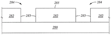
Fig. 2B-2D are side cross-sectional views of features formed on a surface of a substrate using the frames discussed in connection with fig. 2A.
Fig. 3 is a histogram comparing the wet etch rate on a silicon substrate to the wet etch rate on a silicon nitride substrate.
FIG. 4 is a schematic cross-sectional view of a film deposited according to one embodiment.
FIG. 5 is a method for depositing a directional processing film selective to silicon oxide, according to one embodiment.
Fig. 6 is a schematic cross-sectional view of a substrate with patterned features for selective deposition according to one embodiment.
To facilitate understanding, identical reference numerals have been used, where possible, to designate identical elements that are common to the figures. It is contemplated that elements and features of one embodiment may be beneficially utilized on other embodiments without further recitation.
Detailed Description
Embodiments described herein generally provide a method for filling features formed on a substrate. In particular, the described embodiments generally provide for selectively depositing silicon oxide material in dielectric-containing patterned features on a substrate.
FIG. 1 is a schematic cross-sectional view of a processing chamber 100 for selectively depositing films according to one embodiment. In one configuration, the processing chamber 100 may comprise a producer gt chamber, available from applied materials, santa clara, ca. Generally, the processing chamber 100 includes two processing regions 118, 120. The chamber body 102 includes a sidewall 112, an inner wall 114, and a bottom wall 116, the sidewall 112, inner wall 114, and bottom wall 116 defining processing regions 118, 120. The bottom wall 116 in each processing region 118, 120 defines at least two channels 122, 124 through which rods (stem)126 of a heater pedestal 128 and rods (rod)130 of a wafer lift pin assembly are respectively disposed.
The sidewall 112 and the inner wall 114 define two cylindrical annular processing regions 118, 120. Peripheral pumping channels 125 are formed in the chamber walls defining the processing regions 118, 120, the peripheral pumping channels 125 serving to evacuate gases from the processing regions 118, 120 and control the pressure within each region 118, 120. The pumping channel 125 of each processing region 118, 120 is preferably connected to a shared exhaust pump via a shared exhaust channel (not shown) and an exhaust conduit (not shown). Each zone is preferably evacuated to a selected pressure via a pump and an exhaust system connected to allow equalization of pressure within each zone. The pressure in the processing chamber during operation may be between 200Torr and 700 Torr.
Each processing region 118, 120 preferably includes a gas distribution assembly 108 disposed through the chamber lid 104 to deliver gases into the processing region 118, 120. The gas distribution assembly 108 of each processing region includes a gas inlet passage 140, and the gas inlet passage 140 delivers gas into a showerhead assembly 142. A gas source (not shown) is connected to the gas inlet channel 140 and is configured to deliver one or more precursor gases (e.g., TEOS, ozone, ammonia) and/or inert gases (e.g., nitrogen) through the showerhead assembly 142 to the processing regions 118 and 120. An RF feedthrough (feed through) provides a bias potential to the showerhead assembly 142 to facilitate generation of a plasma between the showerhead assembly 142 and the heater pedestal 128.
A heater pedestal 128 is movably disposed in each processing region 118, 120 by a stem 126, the stem 126 being connected to the underside of the support plate and extending through the bottom of the chamber body 102, the stem 126 being connected to the drive system 103 at the bottom of the chamber body 102. The rod 126 moves up and down in the chamber 106 to move the heater pedestal 128 to position a wafer thereon or remove a wafer therefrom for processing.
The chamber body 102 defines a plurality of vertical gas passages for the delivery of various reactant and purge gases suitable for a selected process within the chamber through the gas distribution assembly 108. A gas inlet connection 141 is provided at the bottom of the chamber 106 to connect the gas passage formed in the chamber wall to the gas inlet line 139. The gas inlet line 139 is then connected to a gas source line (not shown) and is controlled for delivering gas to each processing region 118, 120.
The vacuum control system used in the disclosed processing chamber 100 may include a plurality of vacuum pumps in communication with each zone of the processing chamber 100, where each zone has its own set point pressure. The RF power delivery system is used to deliver RF energy to each of the processing regions 118, 120 through each of the gas distribution assemblies 108.
Fig. 2A is a block diagram 200 of a method of selectively depositing a silicon oxide layer according to one embodiment. Fig. 2B-2D are side cross-sectional views of features formed on the surface of substrate 280 by the blocks discussed next in connection with fig. 2A. At block 210, the silicon wafer is precleaned in preparation for deposition. Pre-cleaning may be necessary in some cases because the bare silicon oxidizes in air and forms an undesirable native oxide layer. To ensure good results, the wafer surface may be stripped of the native oxide layer and replaced with a hydrogen-terminated surface using a wet or dry cleaning process.
At block 220, a silicon-containing layer 282 is deposited on the silicon substrate 280. The silicon-containing layer 282 may comprise, for example, silicon oxide (SiO)2) Or silicon nitride (SiN). Such a silicon-containing layer 282 may be deposited by flowing a silicon precursor and oxygen or nitrogen or plasma into the processing chamber.
At block 230, the silicon-containing layer is patterned, resulting in one or more features 284 being formed in the silicon-containing dielectric layer 282. The patterning process may include, for example, applying a photoresist (photoresist), exposing and developing the photoresist (develoop) to form a pattern on the silicon-containing layer, wet or dry etching the exposed portions of the silicon-containing layer, removing the photoresist, and cleaning the patterned surface (e.g., objects 281, 283, and 285 in fig. 2C) in preparation for additional processing. One of ordinary skill in the art will appreciate that the patterning process may vary depending on the particular conditions and goals of the process.
If the silicon-containing layer 282 is formed using silane precursors at block 220, the resulting silicon oxide layer may have high-order silicon-hydrogen bonding. A typical deposition process may include delivering monosilane SiH4Molecular oxygen O2And H2Although it should be understood that other flows may be usedA body gas. The selective deposition of silicon oxide in the patterned features 284 formed in the silicon-containing layer 282, which is performed at a later block, is at least partially dependent upon the silicon-containing deposited dielectric layer 282 having little or no hydrogen bonding at its exposed surfaces. Thus, any silicon oxide-containing layer having hydrogen-terminated surfaces (e.g., a silane-formed silicon-containing layer) may require further processing to prevent deposition growth of a selectively deposited silicon oxide film on these surfaces (e.g., feature sidewalls and field regions) during block 250. In some embodiments, further processing may include, during block 240, exposing the patterned surface of the silicon-containing layer (which was formed during block 220) to a plasma to replace the hydrogen-terminated surface. For example, the plasma treatment at block 240 may include exposing a surface of the silicon-containing layer to a solution containing NH3Or N2To hydrogen bond from the formed silicon-containing layer (e.g., SiO)2Layer) is removed.
Alternatively, a silicon-containing layer 282 deposited at frame 220 can be formed using a Tetraethoxysilane (TEOS) precursor to form a dielectric layer, such as SiO2Or a SiN layer. It is believed that silicon-containing layer 282 formed using TEOS precursors will have significantly less or no hydrogen bonds on its surface so that the optional plasma treatment in block 240 may be omitted.
At block 250, a silicon oxide layer 286 is selectively deposited in the patterned features 284. By mixing TEOS and ozone (O)3) Flows into the processing chamber to deposit the silicon oxide layer 286. The deposition process may be a thermal process or a plasma enhanced process. The thermal treatment may be performed using a deposition process using ozone (O) in a temperature range of about 350-500 ℃ and a pressure range of 20to 620Torr3) And TEOS. In plasma enhanced processing, a controlled plasma may be formed in the vicinity of the substrate 280 by RF energy applied from an RF power supply. Tetraethoxysilane (TEOS) may be flowed into the processing chamber at a rate between about 400 milligrams per minute and 2 grams per minute. Ozone may be flowed into the processing chamber at a rate of about 10% to about 18% by mass.
Because the height of feature 284 can be much greater than the width of feature 284, it is important to ensure that feature 284 fills from the bottom up. If growth occurs on the sidewalls 283 of the features 284, voids or seams may be created which result in less uniform and therefore less reliable integrated circuits. For example, fig. 7 depicts an aperture 350, the aperture 350 may result from growth on the sidewall 283 of the feature 284 rather than simple bottom-up growth.
It has been observed that the selective deposition process performed during block 250 can minimize or prevent the formation of voids and seams by creating growth conditions on the bottom 281 of the features 284 and limited or no growth conditions on the sidewalls 283 of the features 284. In this embodiment, the features 284 (in which the selectively deposited film is formed) are comprised of silicon oxide or silicon nitride or a combination thereof. Due to post-processing of the patterned dielectric layer formed in block 220 or the use of a particular type of patterned silicon oxide layer (i.e., TEOS-based layer) formed in block 220, the surface of the patterned silicon-containing layer will have fewer Si-H bonds and thus provide fewer nucleation points for promoting the initiation of growth of the selectively deposited layer. In contrast, the bottom 281 of the feature 284 (fig. 2D), which may be considered a deposition surface, may be comprised of silicon, which has a high degree of Si-H bonding, and thus provides many nucleation points to promote growth. Thus, in block 250, the TEOS and ozone treatment causes deposition to preferentially occur on the bottom 281 of the features 284 where the substrate 280 is composed of silicon. The selectively deposited silicon oxide layer 286 (figure 2D) of TEOS and ozone does not adhere well to the sidewalls 283 of the features 284, the sidewalls 283 of the features 284 being comprised of silicon nitride, silicon oxide, or a combination thereof. Thus, the silicon oxide layer 286 selectively deposited using TEOS and ozone preferentially forms and adheres to the silicon substrate 280, resulting in uniform growth of the silicon oxide layer from bottom to top without significant growth or adhesion to the sidewalls 283. This treatment results in the minimization of porosity.
A substrate with Si-H bonds on its surface will provide nucleation sites that allow uniform or conformal (conformal) growth on the substrate surface. Without the growth promoted by Si-H bonds, any growth of the selectively deposited layer on these types of surfaces will be non-uniform or island-like. Because growth occurs preferentially on the substrate 280, growth begins at the bottom 281 (i.e., deposition surface) of the patterned features 284 on the surface of the substrate 280. This results in uniform growth of the silicon oxide layer 286 with minimal voids. By comparison, the silicon oxide formed by the process disclosed in block 250 is not uniformly deposited, e.g., on a silicon nitride surface or on the surface of a conventional thermal silicon oxide layer. As such, the silicon oxide layer 286 is selectively grown from the bottom 281 of the patterned features 284, reducing porosity by using a bottom-up fill process.
In some embodiments, the silicon oxide layer 286 formed during block 250 may undesirably adhere to and grow on the sidewalls 283 of the features 284 (e.g., trenches). To address this issue, at block 260, the selectively deposited silicon oxide layer may be optionally etched using dilute hydrofluoric acid (DHF) to remove the low quality and thin formation layer on the sidewalls 283 and field regions (field regions) 285. After this optional etch in block 260, the substrate may again be subjected to the selective deposition process of block 250. These two blocks may be repeated periodically to improve selectivity in, for example, nitride-capped (nitride-capped) features, as discussed below.
Following the selective deposition of the silicon oxide layer at block 250 and the optional periodic deposition and etching at block 260, the substrate may optionally be annealed, such as by thermal treatment using a lamp or other heat source, at block 270. During the anneal block 270, the temperature in the substrate may be between 300 degrees celsius and 480 degrees celsius. The substrate may be optionally etched by dry etching or wet etching.
One advantage of the selective deposition of silicon oxide is the relative improvement in the wet etch rate of the film formed during block 250. In general, a higher wet etch rate may represent a lower density and/or higher porosity of the dielectric material. Thus, compared to SiN on a Si surface, SiO on a Si surfacexMuch lower wet etch rates of the SiO layer manifest themselves in improved uniformity and hence higher quality of the SiO layer. Fig. 3A and 3B illustrate the utility of etching a selectively deposited silicon oxide layer. In fig. 3A, a silicon-containing layer 310 is deposited on a substrate 300, as in block 220 of fig. 2A. The silicon-containing layer 310 is patterned to form features 320, as in block 230 of fig. 2A. Next, a silicon nitride cap 330 is provided on the patterned silicon-containing layer 310. The processing for this block is discussed in more detail below. Next, a silicon oxide layer 340 is selectively deposited in the features 320 of the patterned silicon-containing layer 310, as in block 250 of fig. 2A. As discussed, the silicon oxide layer 340 formed in the feature 320 is a high quality layer due to the selective preferential growth and formation of layers of silicon oxide on the silicon substrate. In fig. 3B, the film is then etched, which can be accomplished by exposure to 100:1 DHF. Due to the poor quality and low density of the silicon oxide layer 340 from the silicon nitride cap 330, DHF preferentially etches the silicon oxide layer 340 from the silicon nitride cap 330 while the silicon oxide layer 340 residing in the feature 320 adjacent to the silicon-containing layer 310 remains intact due to its improved material properties.
Fig. 4 is a histogram comparing the wet etch rate on a silicon substrate to the wet etch rate on a silicon nitride substrate. FIG. 4 assumes a wet etch condition of 100:1 DHF. As shown in fig. 4, the DHF wet etch rate for SiN is more than twice the DHF wet etch rate for Si. Thus, the much lower wet etch rate of SiO on Si surface compared to SiN on Si surface manifests itself in an improved uniformity and thus higher quality of the SiO layer. In other words, the film quality of the selectively grown film layer is high relative to the portion of the selectively grown film formed on the nitride film or the oxide film not to be prepared.
Figures 5A-5D illustrate a method for selective deposition of a directional handle film for silicon oxide to form a silicon nitride cap 330 on top of the patterned silicon-containing layer 310, according to one embodiment. An advantage of the silicon nitride cap 330 is that SiO deposition on the sidewalls of the features 320 is prevented during the processing described in connection with block 250, resulting in enhanced bottom-up feature filling with minimized voids and improved quality of the resulting film. One method for depositing the silicon nitride cap 330 is by directionally processing the substrate with a nitride-containing plasma. An example of such a nitride-containing plasma may be NH3Or N2. Fig. 5A shows the patterned substrate before performing the nitridation process.
In fig. 5B, a plasma 510 is directed at the patterned silicon-containing layer 310 from an angle. The patterned silicon-containing layer 310 shields the lower portions of adjacent features from the directional plasma process, thereby forming a shadowing effect. Thus, only the top portion of each feature 320 is exposed to the directional plasma treatment.
In fig. 5C, the plasma 510 is directed at the patterned si-containing layer 310 from another angle or the substrate is rotated relative to the impinging beam to ensure uniform nitridation process is performed on the surface of the substrate.
In fig. 5D, the directional plasma treatment thus produces the silicon-containing layer 310 having the feature 320, wherein a top portion of the patterned silicon-containing layer 320 is nitrided. Because of the preferential growth of silicon oxide on the silicon substrate, rather than the preferential growth of silicon nitride, when the directionally processed substrate is exposed to the precursor gas described in block 250, the resulting silicon oxide film begins to preferentially grow at the surface of the silicon substrate to fill the features. This bottom-up growth preferential growth prevents growth from the sidewalls and produces a higher quality film with minimal porosity in the features 320.
In some embodiments, to achieve the desired preferential growth, the surface area of the nitride cap 330 may be formed on the substrate 310 such that it amounts to at least about one-third of the total surface area of the features 320. Figure 6 is a schematic cross-sectional view of a substrate 300 having a patterned silicon-containing layer 310 and features 320 for selective deposition according to one embodiment, wherein the nitride caps 330 have a surface area totaling at least about one-third of the surface area of the features 320.
Disclosed embodiments of the invention provide for preferential bottom-up growth of silicon oxide by selective deposition of silicon oxide films using TEOS and ozone at sub-atmospheric pressure. The oxide film deposited by this process grew on the bare silicon surface and showed no growth/island growth on the silicon nitride and thermal oxide surfaces. Because of the preferential growth of silicon oxide on the silicon substrate, rather than the preferential growth of silicon nitride, when the directionally processed substrate is exposed to precursor gases, the resulting silicon oxide film begins to preferentially grow at the surface of the silicon substrate to fill the features. This bottom-up growth preferential growth prevents growth from the sidewalls and produces a higher quality film with minimal porosity in the features.
While the foregoing is directed to embodiments of the present disclosure, other and further embodiments of the disclosure may be devised without departing from the basic scope thereof, and the scope thereof is determined by the claims that follow.
Claims (15)
1. A method for selectively forming a silicon oxide layer on a substrate, comprising:
selectively depositing a silicon oxide layer in patterned features formed on a surface of a substrate, wherein
The patterned features comprising one or more sidewalls and a deposition surface at the bottom of the patterned features, and each of the sidewalls having a cap portion and a cap portion, wherein the cap portion comprises silicon nitride and the cap portion comprises silicon oxide, and the surface area of the cap portion is at least one third of the surface area of the sidewalls and the surface area of the cap portion is at least a portion of the surface area of the sidewalls,
wherein the deposition surface consists essentially of silicon, an
A selectively deposited silicon oxide layer is formed on the deposition surface by exposing the patterned features to Tetraethoxysilane (TEOS) and ozone to fill the patterned features from the bottoms of the patterned features such that the selectively deposited silicon oxide layer is adjacent the base portions and the cap portions.
2. The method of claim 1, further comprising the steps of:
after selectively depositing a silicon oxide layer in the patterned features, the selectively deposited silicon oxide layer is annealed.
3. The method of claim 2, further comprising the steps of:
wet etching the silicon oxide layer after annealing the selectively deposited silicon oxide layer.
4. The method of claim 1, wherein the ozone flows into a processing chamber at a mass flow rate ratio of 10% to 18% of a total mass flow rate of the TEOS and the ozone.
5. The method of claim 1, wherein the TEOS and the ozone are flowed into a processing chamber and a pressure in the processing chamber during operation is between 200Torr and 700 Torr.
6. The method of claim 1, further comprising the steps of:
exposing the patterned feature to a nitrogen-containing plasma prior to selectively depositing a silicon oxide layer in the patterned feature.
7. The method of claim 6, wherein exposing the patterned feature to a nitrogen-containing plasma comprises: the patterned features are directionally treated with an ion beam formed from a nitrogen-containing plasma.
8. A method for selectively forming a silicon oxide layer on a substrate, comprising:
selectively depositing a silicon oxide layer in patterned features formed on a surface of a substrate, wherein
The patterned features comprising one or more sidewalls and a deposition surface at a bottom of the patterned features, and each of the sidewalls having a pedestal portion and a cap portion, wherein the cap portion comprises silicon nitride and the pedestal portion comprises silicon oxide,
the deposition surface consists essentially of silicon, an
A selectively deposited silicon oxide layer is formed on the deposition surface by:
flowing Tetraethoxysilane (TEOS) and ozone over the patterned features to fill the patterned features from the bottoms of the patterned features such that the selectively deposited silicon oxide layer is adjacent the base portion and the cap portion;
after filling the patterned features, etching the selectively deposited silicon oxide layer to preferentially etch the selectively deposited silicon oxide layer from the cap portions in the patterned features while the selectively deposited silicon oxide layer along the base portions remains intact; and
repeating the steps of flowing Tetraethoxysilane (TEOS) and ozone over the patterned features and etching the selectively deposited silicon oxide layer.
9. The method of claim 8, further comprising the steps of:
after selectively depositing a silicon oxide layer in patterned features formed on a surface of the substrate, the selectively deposited silicon oxide layer is annealed.
10. The method of claim 8, further comprising the steps of:
wet etching the silicon oxide layer after annealing the selectively deposited silicon oxide layer.
11. The method of claim 8, wherein the ozone flows into a processing chamber at a mass flow rate ratio of 10% to 18% of a total mass flow rate of the TEOS and the ozone.
12. The method of claim 8, wherein the TEOS and the ozone are flowed into a processing chamber and a pressure in the processing chamber during operation is between 200Torr and 700 Torr.
13. The method of claim 8, further comprising the steps of:
a nitrogen-containing plasma is flowed over a patterned feature formed on a surface of a substrate prior to selectively depositing a silicon oxide layer in the patterned feature.
14. The method of claim 13, wherein flowing a nitrogen-containing plasma over the patterned features comprises: directionally treating the patterned features with a nitrogen-containing plasma.
15. A method for selectively forming a silicon oxide layer on a substrate, comprising:
selectively depositing a silicon oxide layer in patterned features formed on a surface of a substrate, wherein
The patterned features comprising one or more sidewalls and a deposition surface at the bottom of the patterned features, and each of the sidewalls having a base portion and a cap portion,
the cap portion of the one or more sidewalls comprises silicon nitride and the base portion comprises silicon oxide,
the surface area of the cap portion comprises at least one third of the surface area of the sidewall and the surface area of the base portion is at least a portion of the surface area of the sidewall,
the deposition surface consists essentially of silicon, an
A selectively deposited silicon oxide layer formed on the deposition surface by flowing Tetraethoxysilane (TEOS) and ozone over the patterned features; and
after selectively depositing a silicon oxide layer in patterned features formed on a surface of the substrate, the selectively deposited silicon oxide layer is annealed.
Priority Applications (1)
| Application Number | Priority Date | Filing Date | Title |
|---|---|---|---|
| CN202111288200.8A CN114121605A (en) | 2015-06-26 | 2016-06-01 | Selective deposition of silicon oxide films |
Applications Claiming Priority (3)
| Application Number | Priority Date | Filing Date | Title |
|---|---|---|---|
| US201562185388P | 2015-06-26 | 2015-06-26 | |
| US62/185,388 | 2015-06-26 | ||
| PCT/US2016/035302 WO2016209570A1 (en) | 2015-06-26 | 2016-06-01 | Selective deposition of silicon oxide films |
Related Child Applications (1)
| Application Number | Title | Priority Date | Filing Date |
|---|---|---|---|
| CN202111288200.8A Division CN114121605A (en) | 2015-06-26 | 2016-06-01 | Selective deposition of silicon oxide films |
Publications (2)
| Publication Number | Publication Date |
|---|---|
| CN107660307A CN107660307A (en) | 2018-02-02 |
| CN107660307B true CN107660307B (en) | 2021-11-05 |
Family
ID=57586127
Family Applications (2)
| Application Number | Title | Priority Date | Filing Date |
|---|---|---|---|
| CN201680028403.4A Active CN107660307B (en) | 2015-06-26 | 2016-06-01 | Selective deposition of silicon oxide films |
| CN202111288200.8A Pending CN114121605A (en) | 2015-06-26 | 2016-06-01 | Selective deposition of silicon oxide films |
Family Applications After (1)
| Application Number | Title | Priority Date | Filing Date |
|---|---|---|---|
| CN202111288200.8A Pending CN114121605A (en) | 2015-06-26 | 2016-06-01 | Selective deposition of silicon oxide films |
Country Status (6)
| Country | Link |
|---|---|
| US (1) | US10176980B2 (en) |
| JP (1) | JP6920219B2 (en) |
| KR (1) | KR102377376B1 (en) |
| CN (2) | CN107660307B (en) |
| TW (1) | TWI716414B (en) |
| WO (1) | WO2016209570A1 (en) |
Families Citing this family (9)
| Publication number | Priority date | Publication date | Assignee | Title |
|---|---|---|---|---|
| US10176984B2 (en) * | 2017-02-14 | 2019-01-08 | Lam Research Corporation | Selective deposition of silicon oxide |
| US10242866B2 (en) | 2017-03-08 | 2019-03-26 | Lam Research Corporation | Selective deposition of silicon nitride on silicon oxide using catalytic control |
| US10043656B1 (en) * | 2017-03-10 | 2018-08-07 | Lam Research Corporation | Selective growth of silicon oxide or silicon nitride on silicon surfaces in the presence of silicon oxide |
| US9911595B1 (en) | 2017-03-17 | 2018-03-06 | Lam Research Corporation | Selective growth of silicon nitride |
| US10559461B2 (en) | 2017-04-19 | 2020-02-11 | Lam Research Corporation | Selective deposition with atomic layer etch reset |
| JP7203515B2 (en) | 2017-06-06 | 2023-01-13 | アプライド マテリアルズ インコーポレイテッド | Bottom-up growth of silicon oxide and silicon nitride using a sequential deposition-etch-processing method |
| US10460930B2 (en) | 2017-11-22 | 2019-10-29 | Lam Research Corporation | Selective growth of SiO2 on dielectric surfaces in the presence of copper |
| CN112005343A (en) | 2018-03-02 | 2020-11-27 | 朗姆研究公司 | Selective deposition using hydrolysis |
| US10354859B1 (en) * | 2018-03-14 | 2019-07-16 | Sandisk Technologies Llc | Three-dimensional resistive random access memory device containing selectively grown amorphous silicon-containing barrier and method of making the same |
Citations (4)
| Publication number | Priority date | Publication date | Assignee | Title |
|---|---|---|---|---|
| CN103839868A (en) * | 2014-02-21 | 2014-06-04 | 上海华力微电子有限公司 | Manufacturing method for shallow-trench isolation structure |
| US8853019B1 (en) * | 2013-03-13 | 2014-10-07 | Globalfoundries Inc. | Methods of forming a semiconductor device with a nanowire channel structure by performing an anneal process |
| CN104091780A (en) * | 2014-07-25 | 2014-10-08 | 上海华力微电子有限公司 | Self-alignment STI forming method |
| US8912612B2 (en) * | 2013-02-25 | 2014-12-16 | International Business Machines Corporation | Silicon nitride gate encapsulation by implantation |
Family Cites Families (21)
| Publication number | Priority date | Publication date | Assignee | Title |
|---|---|---|---|---|
| JPH08213382A (en) * | 1995-02-02 | 1996-08-20 | Mitsubishi Electric Corp | Semiconductor device and its manufacture |
| JPH11307625A (en) * | 1998-04-24 | 1999-11-05 | Hitachi Ltd | Semiconductor device and manufacture thereof |
| US6413826B2 (en) * | 1999-04-07 | 2002-07-02 | Vantis Corporation | Gate insulator process for nanometer MOSFETS |
| US6235354B1 (en) * | 1999-11-01 | 2001-05-22 | United Microelectronics Corp. | Method of forming a level silicon oxide layer on two regions of different heights on a semiconductor wafer |
| US6429092B1 (en) | 2000-06-19 | 2002-08-06 | Infineon Technologies Ag | Collar formation by selective oxide deposition |
| US6541401B1 (en) * | 2000-07-31 | 2003-04-01 | Applied Materials, Inc. | Wafer pretreatment to decrease rate of silicon dioxide deposition on silicon nitride compared to silicon substrate |
| US6444528B1 (en) | 2000-08-16 | 2002-09-03 | Fairchild Semiconductor Corporation | Selective oxide deposition in the bottom of a trench |
| US6503851B2 (en) | 2000-08-31 | 2003-01-07 | Micron Technology, Inc. | Use of linear injectors to deposit uniform selective ozone TEOS oxide film by pulsing reactants on and off |
| US6368986B1 (en) | 2000-08-31 | 2002-04-09 | Micron Technology, Inc. | Use of selective ozone TEOS oxide to create variable thickness layers and spacers |
| KR100413829B1 (en) * | 2001-03-23 | 2003-12-31 | 삼성전자주식회사 | Trench Isolation Structure and Method for Fabricating the Same |
| US6566227B2 (en) * | 2001-08-13 | 2003-05-20 | Infineon Technologies Ag | Strap resistance using selective oxidation to cap DT poly before STI etch |
| US7625603B2 (en) * | 2003-11-14 | 2009-12-01 | Robert Bosch Gmbh | Crack and residue free conformal deposited silicon oxide with predictable and uniform etching characteristics |
| US7790633B1 (en) * | 2004-10-26 | 2010-09-07 | Novellus Systems, Inc. | Sequential deposition/anneal film densification method |
| US8232176B2 (en) * | 2006-06-22 | 2012-07-31 | Applied Materials, Inc. | Dielectric deposition and etch back processes for bottom up gapfill |
| US20080299775A1 (en) * | 2007-06-04 | 2008-12-04 | Applied Materials, Inc. | Gapfill extension of hdp-cvd integrated process modulation sio2 process |
| US7745350B2 (en) * | 2007-09-07 | 2010-06-29 | Applied Materials, Inc. | Impurity control in HDP-CVD DEP/ETCH/DEP processes |
| US8012887B2 (en) * | 2008-12-18 | 2011-09-06 | Applied Materials, Inc. | Precursor addition to silicon oxide CVD for improved low temperature gapfill |
| JP2011066303A (en) * | 2009-09-18 | 2011-03-31 | Elpida Memory Inc | Method of manufacturing semiconductor device |
| JP2012028420A (en) * | 2010-07-20 | 2012-02-09 | Toshiba Corp | Semiconductor device and manufacturing method of the same |
| CN102479742A (en) * | 2010-11-30 | 2012-05-30 | 中国科学院微电子研究所 | Substrate for integrated circuit and formation method thereof |
| US20130252440A1 (en) * | 2011-09-26 | 2013-09-26 | Applied Materials, Inc. | Pretreatment and improved dielectric coverage |
-
2016
- 2016-06-01 WO PCT/US2016/035302 patent/WO2016209570A1/en active Application Filing
- 2016-06-01 CN CN201680028403.4A patent/CN107660307B/en active Active
- 2016-06-01 CN CN202111288200.8A patent/CN114121605A/en active Pending
- 2016-06-01 JP JP2017567078A patent/JP6920219B2/en active Active
- 2016-06-01 KR KR1020187002530A patent/KR102377376B1/en active IP Right Grant
- 2016-06-17 US US15/185,282 patent/US10176980B2/en active Active
- 2016-06-24 TW TW105119859A patent/TWI716414B/en active
Patent Citations (4)
| Publication number | Priority date | Publication date | Assignee | Title |
|---|---|---|---|---|
| US8912612B2 (en) * | 2013-02-25 | 2014-12-16 | International Business Machines Corporation | Silicon nitride gate encapsulation by implantation |
| US8853019B1 (en) * | 2013-03-13 | 2014-10-07 | Globalfoundries Inc. | Methods of forming a semiconductor device with a nanowire channel structure by performing an anneal process |
| CN103839868A (en) * | 2014-02-21 | 2014-06-04 | 上海华力微电子有限公司 | Manufacturing method for shallow-trench isolation structure |
| CN104091780A (en) * | 2014-07-25 | 2014-10-08 | 上海华力微电子有限公司 | Self-alignment STI forming method |
Non-Patent Citations (2)
| Title |
|---|
| Kap-Duk Song.NO x gas response characteristics of thin film mixed oxide semiconductor.《 Sensors & Actuators: B. Chemical》.2004, * |
| 深亚微米隔离技术――浅沟槽隔离工艺;王新柱等;《半导体学报》;20020308(第03期);全文 * |
Also Published As
| Publication number | Publication date |
|---|---|
| US10176980B2 (en) | 2019-01-08 |
| KR20180014204A (en) | 2018-02-07 |
| WO2016209570A1 (en) | 2016-12-29 |
| JP6920219B2 (en) | 2021-08-18 |
| TWI716414B (en) | 2021-01-21 |
| CN114121605A (en) | 2022-03-01 |
| CN107660307A (en) | 2018-02-02 |
| TW201710539A (en) | 2017-03-16 |
| JP2018524814A (en) | 2018-08-30 |
| US20170004974A1 (en) | 2017-01-05 |
| KR102377376B1 (en) | 2022-03-21 |
Similar Documents
| Publication | Publication Date | Title |
|---|---|---|
| CN107660307B (en) | Selective deposition of silicon oxide films | |
| US11676812B2 (en) | Method for forming silicon nitride film selectively on top/bottom portions | |
| CN110431661B (en) | Two-step process for gap filling high aspect ratio trenches with amorphous silicon films | |
| US7718553B2 (en) | Method for forming insulation film having high density | |
| TWI780160B (en) | Bottom-up growth of silicon oxide and silicon nitride using sequential deposition-etch-treat processing | |
| US10811303B2 (en) | Methods for gapfill in high aspect ratio structures | |
| CN110476239B (en) | Gap filling using reactive annealing | |
| CN110546753B (en) | Method for gap filling in high aspect ratio structure | |
| CN110476222B (en) | Two-step process for silicon gap filling | |
| TW201740448A (en) | Substrate processing method using free radicals in plasma obtained from a mixed gas of the NF3 gas and the NH3 gas to etch | |
| CN110431660B (en) | Surface modification to improve amorphous silicon gap filling | |
| KR20220059967A (en) | Methods and apparatus for depositing dielectric material | |
| CN116982139A (en) | Gap filling process using pulsed High Frequency Radio Frequency (HFRF) plasma | |
| KR102650586B1 (en) | Low deposition rates for flowable PECVD | |
| JP2023057062A (en) | Methods for seamless gap filling using gradient oxidation |
Legal Events
| Date | Code | Title | Description |
|---|---|---|---|
| PB01 | Publication | ||
| PB01 | Publication | ||
| SE01 | Entry into force of request for substantive examination | ||
| SE01 | Entry into force of request for substantive examination | ||
| GR01 | Patent grant | ||
| GR01 | Patent grant |