CN107073677B - Printing chemical mechanical polishing pad - Google Patents
Printing chemical mechanical polishing pad Download PDFInfo
- Publication number
- CN107073677B CN107073677B CN201580056353.6A CN201580056353A CN107073677B CN 107073677 B CN107073677 B CN 107073677B CN 201580056353 A CN201580056353 A CN 201580056353A CN 107073677 B CN107073677 B CN 107073677B
- Authority
- CN
- China
- Prior art keywords
- layer
- polishing
- polishing pad
- abrasive
- additive
- Prior art date
- Legal status (The legal status is an assumption and is not a legal conclusion. Google has not performed a legal analysis and makes no representation as to the accuracy of the status listed.)
- Active
Links
- 238000005498 polishing Methods 0.000 title claims abstract description 174
- 239000000126 substance Substances 0.000 title claims description 12
- 238000007639 printing Methods 0.000 title description 3
- 239000000463 material Substances 0.000 claims abstract description 105
- 239000000654 additive Substances 0.000 claims abstract description 70
- 238000000034 method Methods 0.000 claims abstract description 43
- 230000000996 additive effect Effects 0.000 claims abstract description 42
- 238000000151 deposition Methods 0.000 claims abstract description 14
- 238000004519 manufacturing process Methods 0.000 claims abstract description 12
- 239000002243 precursor Substances 0.000 claims description 24
- 239000002105 nanoparticle Substances 0.000 claims description 9
- 238000005299 abrasion Methods 0.000 claims description 4
- 239000010410 layer Substances 0.000 description 126
- 239000000758 substrate Substances 0.000 description 30
- 239000002245 particle Substances 0.000 description 25
- 230000008569 process Effects 0.000 description 16
- 239000000843 powder Substances 0.000 description 11
- 238000010146 3D printing Methods 0.000 description 9
- 230000008021 deposition Effects 0.000 description 7
- 239000000203 mixture Substances 0.000 description 7
- 239000000919 ceramic Substances 0.000 description 6
- 229920002635 polyurethane Polymers 0.000 description 6
- 239000004814 polyurethane Substances 0.000 description 6
- 239000012530 fluid Substances 0.000 description 5
- 239000007788 liquid Substances 0.000 description 5
- 239000011159 matrix material Substances 0.000 description 5
- VYPSYNLAJGMNEJ-UHFFFAOYSA-N Silicium dioxide Chemical compound O=[Si]=O VYPSYNLAJGMNEJ-UHFFFAOYSA-N 0.000 description 4
- 230000008859 change Effects 0.000 description 4
- 239000006260 foam Substances 0.000 description 4
- 238000009472 formulation Methods 0.000 description 4
- 239000000178 monomer Substances 0.000 description 4
- 239000002002 slurry Substances 0.000 description 4
- CNHDIAIOKMXOLK-UHFFFAOYSA-N toluquinol Chemical compound CC1=CC(O)=CC=C1O CNHDIAIOKMXOLK-UHFFFAOYSA-N 0.000 description 4
- OZAIFHULBGXAKX-UHFFFAOYSA-N 2-(2-cyanopropan-2-yldiazenyl)-2-methylpropanenitrile Chemical compound N#CC(C)(C)N=NC(C)(C)C#N OZAIFHULBGXAKX-UHFFFAOYSA-N 0.000 description 3
- 239000002202 Polyethylene glycol Substances 0.000 description 3
- -1 Polytetrafluoroethylene Polymers 0.000 description 3
- 239000004820 Pressure-sensitive adhesive Substances 0.000 description 3
- GWEVSGVZZGPLCZ-UHFFFAOYSA-N Titan oxide Chemical compound O=[Ti]=O GWEVSGVZZGPLCZ-UHFFFAOYSA-N 0.000 description 3
- 239000011230 binding agent Substances 0.000 description 3
- 230000015572 biosynthetic process Effects 0.000 description 3
- 238000006243 chemical reaction Methods 0.000 description 3
- 230000003750 conditioning effect Effects 0.000 description 3
- 238000005516 engineering process Methods 0.000 description 3
- 229910052751 metal Inorganic materials 0.000 description 3
- 239000002184 metal Substances 0.000 description 3
- 229910044991 metal oxide Inorganic materials 0.000 description 3
- 150000004706 metal oxides Chemical class 0.000 description 3
- 239000004005 microsphere Substances 0.000 description 3
- 239000004033 plastic Substances 0.000 description 3
- 229920003023 plastic Polymers 0.000 description 3
- 238000007517 polishing process Methods 0.000 description 3
- 229920001223 polyethylene glycol Polymers 0.000 description 3
- 229920000642 polymer Polymers 0.000 description 3
- 239000003361 porogen Substances 0.000 description 3
- NIXOWILDQLNWCW-UHFFFAOYSA-M Acrylate Chemical compound [O-]C(=O)C=C NIXOWILDQLNWCW-UHFFFAOYSA-M 0.000 description 2
- IJGRMHOSHXDMSA-UHFFFAOYSA-N Atomic nitrogen Chemical compound N#N IJGRMHOSHXDMSA-UHFFFAOYSA-N 0.000 description 2
- VTYYLEPIZMXCLO-UHFFFAOYSA-L Calcium carbonate Chemical compound [Ca+2].[O-]C([O-])=O VTYYLEPIZMXCLO-UHFFFAOYSA-L 0.000 description 2
- RTZKZFJDLAIYFH-UHFFFAOYSA-N Diethyl ether Chemical compound CCOCC RTZKZFJDLAIYFH-UHFFFAOYSA-N 0.000 description 2
- 229920003171 Poly (ethylene oxide) Polymers 0.000 description 2
- FAPWRFPIFSIZLT-UHFFFAOYSA-M Sodium chloride Chemical compound [Na+].[Cl-] FAPWRFPIFSIZLT-UHFFFAOYSA-M 0.000 description 2
- MCMNRKCIXSYSNV-UHFFFAOYSA-N Zirconium dioxide Chemical compound O=[Zr]=O MCMNRKCIXSYSNV-UHFFFAOYSA-N 0.000 description 2
- 230000003213 activating effect Effects 0.000 description 2
- 239000012790 adhesive layer Substances 0.000 description 2
- 229910002113 barium titanate Inorganic materials 0.000 description 2
- 230000008901 benefit Effects 0.000 description 2
- 229910000420 cerium oxide Inorganic materials 0.000 description 2
- 239000002482 conductive additive Substances 0.000 description 2
- 238000001816 cooling Methods 0.000 description 2
- 239000011258 core-shell material Substances 0.000 description 2
- 230000001419 dependent effect Effects 0.000 description 2
- 238000009826 distribution Methods 0.000 description 2
- 230000000694 effects Effects 0.000 description 2
- 230000002708 enhancing effect Effects 0.000 description 2
- UHESRSKEBRADOO-UHFFFAOYSA-N ethyl carbamate;prop-2-enoic acid Chemical compound OC(=O)C=C.CCOC(N)=O UHESRSKEBRADOO-UHFFFAOYSA-N 0.000 description 2
- 239000007789 gas Substances 0.000 description 2
- 238000000227 grinding Methods 0.000 description 2
- 238000001746 injection moulding Methods 0.000 description 2
- 238000003475 lamination Methods 0.000 description 2
- 230000007246 mechanism Effects 0.000 description 2
- 238000002844 melting Methods 0.000 description 2
- 230000008018 melting Effects 0.000 description 2
- 238000000465 moulding Methods 0.000 description 2
- BMMGVYCKOGBVEV-UHFFFAOYSA-N oxo(oxoceriooxy)cerium Chemical compound [Ce]=O.O=[Ce]=O BMMGVYCKOGBVEV-UHFFFAOYSA-N 0.000 description 2
- 229920001343 polytetrafluoroethylene Polymers 0.000 description 2
- 239000004810 polytetrafluoroethylene Substances 0.000 description 2
- 239000011148 porous material Substances 0.000 description 2
- VZOPRCCTKLAGPN-ZFJVMAEJSA-L potassium;sodium;(2r,3r)-2,3-dihydroxybutanedioate;tetrahydrate Chemical compound O.O.O.O.[Na+].[K+].[O-]C(=O)[C@H](O)[C@@H](O)C([O-])=O VZOPRCCTKLAGPN-ZFJVMAEJSA-L 0.000 description 2
- 239000011347 resin Substances 0.000 description 2
- 229920005989 resin Polymers 0.000 description 2
- 150000003839 salts Chemical class 0.000 description 2
- 239000007787 solid Substances 0.000 description 2
- XOLBLPGZBRYERU-UHFFFAOYSA-N tin dioxide Chemical compound O=[Sn]=O XOLBLPGZBRYERU-UHFFFAOYSA-N 0.000 description 2
- WKBPZYKAUNRMKP-UHFFFAOYSA-N 1-[2-(2,4-dichlorophenyl)pentyl]1,2,4-triazole Chemical compound C=1C=C(Cl)C=C(Cl)C=1C(CCC)CN1C=NC=N1 WKBPZYKAUNRMKP-UHFFFAOYSA-N 0.000 description 1
- OZAIFHULBGXAKX-VAWYXSNFSA-N AIBN Substances N#CC(C)(C)\N=N\C(C)(C)C#N OZAIFHULBGXAKX-VAWYXSNFSA-N 0.000 description 1
- 229910016455 AlBN Inorganic materials 0.000 description 1
- 229910002902 BiFeO3 Inorganic materials 0.000 description 1
- OKTJSMMVPCPJKN-UHFFFAOYSA-N Carbon Chemical compound [C] OKTJSMMVPCPJKN-UHFFFAOYSA-N 0.000 description 1
- 229920002134 Carboxymethyl cellulose Polymers 0.000 description 1
- 229920001661 Chitosan Polymers 0.000 description 1
- 229910016555 CuOFe2O3 Inorganic materials 0.000 description 1
- 229910052692 Dysprosium Inorganic materials 0.000 description 1
- 229910015191 FeOFe2O3 Inorganic materials 0.000 description 1
- 229910052688 Gadolinium Inorganic materials 0.000 description 1
- 108010010803 Gelatin Proteins 0.000 description 1
- 229910003334 KNbO3 Inorganic materials 0.000 description 1
- 229910003327 LiNbO3 Inorganic materials 0.000 description 1
- 229910012463 LiTaO3 Inorganic materials 0.000 description 1
- 229910017955 MgOFe2O3 Inorganic materials 0.000 description 1
- 229910016629 MnBi Inorganic materials 0.000 description 1
- 229910016987 MnOFe2O3 Inorganic materials 0.000 description 1
- 229910016964 MnSb Inorganic materials 0.000 description 1
- 229910003237 Na0.5Bi0.5TiO3 Inorganic materials 0.000 description 1
- 229910020347 Na2WO3 Inorganic materials 0.000 description 1
- 229910003378 NaNbO3 Inorganic materials 0.000 description 1
- 229910005857 NiOFe2O3 Inorganic materials 0.000 description 1
- 239000002033 PVDF binder Substances 0.000 description 1
- 229910018949 PtAu Inorganic materials 0.000 description 1
- 229910052581 Si3N4 Inorganic materials 0.000 description 1
- XUIMIQQOPSSXEZ-UHFFFAOYSA-N Silicon Chemical compound [Si] XUIMIQQOPSSXEZ-UHFFFAOYSA-N 0.000 description 1
- 229910002370 SrTiO3 Inorganic materials 0.000 description 1
- 229910009493 Y3Fe5O12 Inorganic materials 0.000 description 1
- 229910045601 alloy Inorganic materials 0.000 description 1
- 239000000956 alloy Substances 0.000 description 1
- PNEYBMLMFCGWSK-UHFFFAOYSA-N aluminium oxide Inorganic materials [O-2].[O-2].[O-2].[Al+3].[Al+3] PNEYBMLMFCGWSK-UHFFFAOYSA-N 0.000 description 1
- 230000009286 beneficial effect Effects 0.000 description 1
- 229910000019 calcium carbonate Inorganic materials 0.000 description 1
- 229910052799 carbon Inorganic materials 0.000 description 1
- 239000006229 carbon black Substances 0.000 description 1
- 239000002041 carbon nanotube Substances 0.000 description 1
- 229910021393 carbon nanotube Inorganic materials 0.000 description 1
- 238000005266 casting Methods 0.000 description 1
- CETPSERCERDGAM-UHFFFAOYSA-N ceric oxide Chemical compound O=[Ce]=O CETPSERCERDGAM-UHFFFAOYSA-N 0.000 description 1
- 229910000422 cerium(IV) oxide Inorganic materials 0.000 description 1
- AYTAKQFHWFYBMA-UHFFFAOYSA-N chromium(IV) oxide Inorganic materials O=[Cr]=O AYTAKQFHWFYBMA-UHFFFAOYSA-N 0.000 description 1
- 229910052681 coesite Inorganic materials 0.000 description 1
- 238000004590 computer program Methods 0.000 description 1
- 239000011370 conductive nanoparticle Substances 0.000 description 1
- 229910052802 copper Inorganic materials 0.000 description 1
- 229910052593 corundum Inorganic materials 0.000 description 1
- 229910052906 cristobalite Inorganic materials 0.000 description 1
- 238000004132 cross linking Methods 0.000 description 1
- 239000013078 crystal Substances 0.000 description 1
- 230000007547 defect Effects 0.000 description 1
- 238000004512 die casting Methods 0.000 description 1
- 239000003085 diluting agent Substances 0.000 description 1
- 238000010894 electron beam technology Methods 0.000 description 1
- 238000000605 extraction Methods 0.000 description 1
- 229910000154 gallium phosphate Inorganic materials 0.000 description 1
- 239000000499 gel Substances 0.000 description 1
- 229920000159 gelatin Polymers 0.000 description 1
- 239000008273 gelatin Substances 0.000 description 1
- 235000019322 gelatine Nutrition 0.000 description 1
- 235000011852 gelatine desserts Nutrition 0.000 description 1
- 229910052737 gold Inorganic materials 0.000 description 1
- CJNBYAVZURUTKZ-UHFFFAOYSA-N hafnium(IV) oxide Inorganic materials O=[Hf]=O CJNBYAVZURUTKZ-UHFFFAOYSA-N 0.000 description 1
- 239000000017 hydrogel Substances 0.000 description 1
- 238000011065 in-situ storage Methods 0.000 description 1
- 239000011261 inert gas Substances 0.000 description 1
- 239000003112 inhibitor Substances 0.000 description 1
- 239000003999 initiator Substances 0.000 description 1
- 238000007641 inkjet printing Methods 0.000 description 1
- 229910052742 iron Inorganic materials 0.000 description 1
- JEIPFZHSYJVQDO-UHFFFAOYSA-N iron(III) oxide Inorganic materials O=[Fe]O[Fe]=O JEIPFZHSYJVQDO-UHFFFAOYSA-N 0.000 description 1
- 239000012705 liquid precursor Substances 0.000 description 1
- 238000001459 lithography Methods 0.000 description 1
- 239000006249 magnetic particle Substances 0.000 description 1
- 239000000155 melt Substances 0.000 description 1
- 239000012528 membrane Substances 0.000 description 1
- 150000002739 metals Chemical class 0.000 description 1
- 238000002156 mixing Methods 0.000 description 1
- 238000012986 modification Methods 0.000 description 1
- 230000004048 modification Effects 0.000 description 1
- 229910052759 nickel Inorganic materials 0.000 description 1
- 229910052757 nitrogen Inorganic materials 0.000 description 1
- TWNQGVIAIRXVLR-UHFFFAOYSA-N oxo(oxoalumanyloxy)alumane Chemical compound O=[Al]O[Al]=O TWNQGVIAIRXVLR-UHFFFAOYSA-N 0.000 description 1
- 239000003002 pH adjusting agent Substances 0.000 description 1
- 230000000704 physical effect Effects 0.000 description 1
- 229910052697 platinum Inorganic materials 0.000 description 1
- 229920003229 poly(methyl methacrylate) Polymers 0.000 description 1
- 238000006116 polymerization reaction Methods 0.000 description 1
- 239000004926 polymethyl methacrylate Substances 0.000 description 1
- 229920001296 polysiloxane Polymers 0.000 description 1
- 229920002981 polyvinylidene fluoride Polymers 0.000 description 1
- 239000010453 quartz Substances 0.000 description 1
- 238000000110 selective laser sintering Methods 0.000 description 1
- 239000004065 semiconductor Substances 0.000 description 1
- 229910052710 silicon Inorganic materials 0.000 description 1
- 239000010703 silicon Substances 0.000 description 1
- 239000000377 silicon dioxide Substances 0.000 description 1
- 229910052814 silicon oxide Inorganic materials 0.000 description 1
- 229910052709 silver Inorganic materials 0.000 description 1
- 239000002356 single layer Substances 0.000 description 1
- 238000005245 sintering Methods 0.000 description 1
- 229910052708 sodium Inorganic materials 0.000 description 1
- 239000011734 sodium Substances 0.000 description 1
- 239000011780 sodium chloride Substances 0.000 description 1
- 229940074446 sodium potassium tartrate tetrahydrate Drugs 0.000 description 1
- MUPJWXCPTRQOKY-UHFFFAOYSA-N sodium;niobium(5+);oxygen(2-) Chemical compound [O-2].[O-2].[O-2].[Na+].[Nb+5] MUPJWXCPTRQOKY-UHFFFAOYSA-N 0.000 description 1
- 239000000243 solution Substances 0.000 description 1
- 238000005507 spraying Methods 0.000 description 1
- 238000003892 spreading Methods 0.000 description 1
- 230000007480 spreading Effects 0.000 description 1
- 229910052682 stishovite Inorganic materials 0.000 description 1
- 238000003786 synthesis reaction Methods 0.000 description 1
- 239000010936 titanium Substances 0.000 description 1
- JMXKSZRRTHPKDL-UHFFFAOYSA-N titanium ethoxide Chemical compound [Ti+4].CC[O-].CC[O-].CC[O-].CC[O-] JMXKSZRRTHPKDL-UHFFFAOYSA-N 0.000 description 1
- XJDNKRIXUMDJCW-UHFFFAOYSA-J titanium tetrachloride Chemical compound Cl[Ti](Cl)(Cl)Cl XJDNKRIXUMDJCW-UHFFFAOYSA-J 0.000 description 1
- 239000011031 topaz Substances 0.000 description 1
- 229910052853 topaz Inorganic materials 0.000 description 1
- 229910052613 tourmaline Inorganic materials 0.000 description 1
- 239000011032 tourmaline Substances 0.000 description 1
- 229940070527 tourmaline Drugs 0.000 description 1
- 230000009466 transformation Effects 0.000 description 1
- 229910052905 tridymite Inorganic materials 0.000 description 1
- 229910001845 yogo sapphire Inorganic materials 0.000 description 1
Images


Classifications
-
- B—PERFORMING OPERATIONS; TRANSPORTING
- B24—GRINDING; POLISHING
- B24B—MACHINES, DEVICES, OR PROCESSES FOR GRINDING OR POLISHING; DRESSING OR CONDITIONING OF ABRADING SURFACES; FEEDING OF GRINDING, POLISHING, OR LAPPING AGENTS
- B24B37/00—Lapping machines or devices; Accessories
- B24B37/11—Lapping tools
- B24B37/20—Lapping pads for working plane surfaces
- B24B37/24—Lapping pads for working plane surfaces characterised by the composition or properties of the pad materials
-
- B—PERFORMING OPERATIONS; TRANSPORTING
- B24—GRINDING; POLISHING
- B24B—MACHINES, DEVICES, OR PROCESSES FOR GRINDING OR POLISHING; DRESSING OR CONDITIONING OF ABRADING SURFACES; FEEDING OF GRINDING, POLISHING, OR LAPPING AGENTS
- B24B37/00—Lapping machines or devices; Accessories
- B24B37/11—Lapping tools
- B24B37/20—Lapping pads for working plane surfaces
- B24B37/22—Lapping pads for working plane surfaces characterised by a multi-layered structure
-
- B—PERFORMING OPERATIONS; TRANSPORTING
- B24—GRINDING; POLISHING
- B24B—MACHINES, DEVICES, OR PROCESSES FOR GRINDING OR POLISHING; DRESSING OR CONDITIONING OF ABRADING SURFACES; FEEDING OF GRINDING, POLISHING, OR LAPPING AGENTS
- B24B37/00—Lapping machines or devices; Accessories
- B24B37/11—Lapping tools
- B24B37/20—Lapping pads for working plane surfaces
- B24B37/24—Lapping pads for working plane surfaces characterised by the composition or properties of the pad materials
- B24B37/245—Pads with fixed abrasives
-
- B—PERFORMING OPERATIONS; TRANSPORTING
- B24—GRINDING; POLISHING
- B24B—MACHINES, DEVICES, OR PROCESSES FOR GRINDING OR POLISHING; DRESSING OR CONDITIONING OF ABRADING SURFACES; FEEDING OF GRINDING, POLISHING, OR LAPPING AGENTS
- B24B37/00—Lapping machines or devices; Accessories
- B24B37/11—Lapping tools
- B24B37/20—Lapping pads for working plane surfaces
- B24B37/26—Lapping pads for working plane surfaces characterised by the shape of the lapping pad surface, e.g. grooved
-
- B—PERFORMING OPERATIONS; TRANSPORTING
- B24—GRINDING; POLISHING
- B24D—TOOLS FOR GRINDING, BUFFING OR SHARPENING
- B24D18/00—Manufacture of grinding tools or other grinding devices, e.g. wheels, not otherwise provided for
- B24D18/0045—Manufacture of grinding tools or other grinding devices, e.g. wheels, not otherwise provided for by stacking sheets of abrasive material
-
- B—PERFORMING OPERATIONS; TRANSPORTING
- B33—ADDITIVE MANUFACTURING TECHNOLOGY
- B33Y—ADDITIVE MANUFACTURING, i.e. MANUFACTURING OF THREE-DIMENSIONAL [3-D] OBJECTS BY ADDITIVE DEPOSITION, ADDITIVE AGGLOMERATION OR ADDITIVE LAYERING, e.g. BY 3-D PRINTING, STEREOLITHOGRAPHY OR SELECTIVE LASER SINTERING
- B33Y10/00—Processes of additive manufacturing
-
- B—PERFORMING OPERATIONS; TRANSPORTING
- B33—ADDITIVE MANUFACTURING TECHNOLOGY
- B33Y—ADDITIVE MANUFACTURING, i.e. MANUFACTURING OF THREE-DIMENSIONAL [3-D] OBJECTS BY ADDITIVE DEPOSITION, ADDITIVE AGGLOMERATION OR ADDITIVE LAYERING, e.g. BY 3-D PRINTING, STEREOLITHOGRAPHY OR SELECTIVE LASER SINTERING
- B33Y80/00—Products made by additive manufacturing
Abstract
A method of manufacturing a polishing layer of a polishing pad, the method comprising sequentially depositing a plurality of layers with a 3D printer, each layer of the plurality of polishing layers being deposited by ejecting a base material from a first nozzle and an additive material from a second nozzle and curing the base material and the additive material to form a cured pad material.
Description
Background
Technical Field
The invention relates to a polishing pad used in chemical mechanical polishing.
Background
Reliable production of nanometer and smaller features is one of the key technical challenges for next generation very large scale integrated circuits (VLSI) and ultra large scale integrated circuits (ULSI) for semiconductor devices. However, as the limits of circuit technology have advanced, the scaling of VLSI and ULSI interconnect technologies has placed additional demands on processing power. Reliable formation of gate structures on substrates is important to the success of VLSI and ULSI and to the continued effort to increase circuit density and quality of individual substrates and dies (die).
Integrated circuits are typically formed on a substrate by the sequential deposition of conductive, semiconductive or insulating layers on a silicon wafer. Various fabrication processes require planarization of layers on a substrate. For example, for certain applications, such as grinding the metal layer to form vias, plugs and lines in trenches of the pattern layer, the overlying layer is planarized until the top surface of the pattern layer is exposed. In other applications, such as planarization of dielectric layers for lithography, an overlying layer is polished until a desired thickness remains over an underlying layer.
Chemical Mechanical Polishing (CMP) is a process commonly used in the manufacture of high density integrated circuits to planarize or polish layers of material deposited on a substrate. The carrier head may provide the substrate held therein to a polishing station of the CMP system and controllably urge the substrate against the moving polishing pad. CMP is effectively applied by providing contact between the feature sides of the substrate and moving the substrate relative to the polishing pad in the presence of the polishing fluid. Material is removed from the feature side of the substrate that contacts the polishing surface by a combination of chemical and mechanical activity.
One purpose of the chemical mechanical polishing process is polishing uniformity. If different areas on the substrate are polished at different rates, there may be either too much material removed ("over-polished") or too little material removed ("under-polished") for certain areas of the substrate. Conventional polishing pads include "standard" pads as well as fixed-abrasive pads. Standard pads have a polyurethane abrasive layer with a durable roughened surface and may also include a compressible backing layer. In contrast, fixed abrasive pads have abrasive particles contained in a containment medium and may be supported on a generally incompressible backing layer. The polishing pad can be uniquely selected depending on the operation and desired result.
The polishing pad is typically made by molding, casting or sintering a polyurethane material. In the case of molding, one polishing pad at a time may be made, for example, by injection molding. In the case of die casting, the liquid precursor is cast and cured (cure) into a block which is then cut into individual gaskets. These shims may then be machined to final thickness. The grooves may be machined into the abrasive surface or formed as part of an injection molding process. The formation of polishing pads is time consuming and requires multiple steps before the polishing pad is acceptable for CMP use.
Accordingly, there is a need for an improved polishing pad.
Disclosure of Invention
A method of manufacturing a polishing pad is disclosed that includes sequentially depositing a plurality of layers with a 3D printer. Each of the plurality of abrasive layers is deposited by ejecting a base material from a first nozzle and an additive material from a second nozzle. The base material and the additive material are cured (soliddify) to form a cured mat material.
Drawings
So that the manner in which the above recited features of the embodiments can be understood in detail, a more particular description of the embodiments, briefly summarized above, may be had by reference to embodiments, some of which are illustrated in the appended drawings. It is to be noted, however, that the appended drawings illustrate only examples of the present embodiments and are therefore not to be considered limiting of its scope, for the disclosure may admit to other equally effective embodiments.
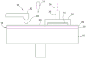
Fig. 1A is a schematic cross-sectional side view of an example polishing pad.
Fig. 1B is a schematic cross-sectional side view of another example polishing pad.
Fig. 1C is a schematic cross-sectional side view of yet another example polishing pad.
Fig. 2 is a schematic side, partial cross-sectional view of a chemical mechanical polishing station.
Fig. 3 is a schematic cross-sectional side view showing a 3D printer for manufacturing the polishing pad of fig. 1A.
To facilitate understanding, identical reference numerals have been used, where possible, to designate identical elements that are common to the figures. It is contemplated that elements and features of one embodiment may be beneficially utilized on other embodiments without further recitation.
Detailed Description
To provide polishing uniformity, the polishing pad needs to make uniform contact with the substrate being polished so that a uniform pressure can be applied across the substrate surface. The thickness variation of the pad may create a non-uniform pressure across the substrate surface. Even small variations in thickness lead to variations in applied pressure and, therefore, non-uniform removal and more serious defects, such as micro-scratches on the substrate surface. This effect is more severe for hard polishing pads and also more severe under low pressure polishing processes. Although soft polishing pads can accommodate greater thickness variations, the process of forming grooves in the pad is more likely to produce non-uniformities in the soft polishing pad.
A technique for manufacturing polishing pads that can provide improved thickness uniformity is 3D printing. In the 3D printing process, a thin layer of pad precursor, such as a liquid, is gradually deposited and melted to form the complete three-dimensional polishing pad.
In one example, a method of manufacturing a polishing layer of a polishing pad includes sequentially depositing a plurality of layers with a 3D printer, each layer of the plurality of polishing layers being deposited by ejecting a liquid pad material precursor from a nozzle and curing the pad material precursor to form a cured pad material.
Implementations of the invention may include one or more of the following features. Each of the plurality of layers may have a thickness that is less than 50% of a total thickness of the polishing layer. Each of the plurality of layers may have a thickness that is less than 1% of a total thickness of the polishing layer. Recesses (reciss) may be formed in the polishing layer by controlling the jetting of the pad material precursor with a 3D mapping program running on a computer to form a pattern in at least some of the plurality of layers. The recess can be 10% to 75% of the total horizontal surface area of the polishing pad. The plateau (plateau) between the notches may have a lateral dimension of 0.1 to 2.5 mm. The recess may have a depth of 0.25 to 1.5 mm. The notch may have a widest lateral dimension of 0.1mm to 2 mm. The recesses may be shaped as one or more of a cylinder, truncated pyramid, or prism. The recess may be a groove. Curing the mat material precursor may include hardening the mat material precursor. Curing the mat material precursor may include Ultraviolet (UV) curing. The mat material precursor may include a urethane acrylate oligomer or an acrylate monomer. The cured mat material may comprise polyurethane. Abrasive particles may be supplied in the solidified pad material. The abrasive particles may be metal oxide particles. The back layer of the polishing pad can be formed by sequentially depositing a plurality of layers with a 3D printer. Forming the backing layer may include hardening the plurality of layers of the backing layer with a different amount than the plurality of layers of the abrasive layer. Forming the backing layer may include injecting a material different from the pad precursor material. The cured abrasive layer may have a Shore D hardness (Shore D hardness) of between about 30 to about 90 in some regions and between about 26 to about 95 in other regions of the pad. The mat material precursor may be a molten mat material and solidifying the mat material precursor may include cooling the molten mat material.
Advantages of the invention may include one or more of the following. The polishing pad can be manufactured with very tight tolerances, such as good thickness uniformity. Grooves can be formed in the polishing pad without distortion (distor) thickness uniformity. Polishing uniformity across the substrate can be improved, particularly at low pressures, such as below 0.8psi, or even below 0.5psi or 0.3 psi. The pad manufacturing process is adaptable to different polishing pad configurations and groove patterns. The polishing pad can be made faster and cheaper.
Referring to fig. 1A-1C, the polishing pad 18 includes a polishing layer 22. The polishing pad 18 may be a single layer pad comprised of a polishing layer 22, as shown in fig. 1A, or the polishing pad 18 may be a multi-layer pad comprising a polishing layer 22 and at least one backing layer 20, as shown in fig. 1C. In one or more embodiments, the backing layer 20 and the abrasive layer 22 may be integrally formed when 3D printing the abrasive pad 18.
The polishing pad 18 may have one or more regions, such as a first region 42, a second region 41, and a third region 43. The regions 42, 41, 43 may be discrete regions having different characteristics. One or more of the regions 42, 41, 43 may have additives incorporated into each region to modify the properties of the polishing pad 18. For example, regions 41 and 43 may be stiffer than region 42. The regions 42, 41, 43 may also have different abrasive, thermal or other properties. This may be achieved by using different types and/or amounts of additives in at least two of the regions 42, 41, 43.
The polishing layer 22 may be a material that is inert during the polishing process. The material of the abrasive layer 22 may be a plastic, such as polyurethane. In some implementations, the polishing layer 22 is a relatively durable and hard material. For example, the polishing layer 22 may have a hardness of about 30 Shore D to about 90 Shore D, such as about 50 Shore D to about 65 Shore D, on the Shore D scale. In other softer regions, the polishing layer 22 may have a Shore A hardness of between about 26 Shore A and 95 Shore A.
The abrasive layer 22 may be a layer of homogenous (homogenous) composition, as shown in fig. 1A, or the abrasive layer 22 may include abrasive particles 28 held in a matrix (matrix)29 of plastic material, such as polyurethane, as shown in fig. 1B. The abrasive particles 28 are harder than the material of the matrix 29. The abrasive particles 28 may comprise about 0.05 weight percent (wt%) to about 75 wt% of the abrasive layer. For example, the abrasive particles 28 may be less than about 1 weight percent of the abrasive layer 22, such as less than about 0.1 weight percent. Alternatively, the abrasive particles 28 may be greater than about 10 weight percent, such as greater than about 50 weight percent, of the abrasive layer 22. The material of the abrasive particles may be a metal oxide such as cerium oxide, aluminum oxide, silicon oxide, or combinations thereof.
The abrasive layer 22 can have a thickness D1 of 80 mils (mil) or less, such as 50 mils or less, such as 25 mils or less. Because conditioning processes tend to wear away the polishing surface 24, the thickness of the polishing layer 22 may be selected to provide an effective useful life of the polishing pad 18, such as 3000 polishing and conditioning cycles.
On a microscopic scale, the abrasive surface 24 of the abrasive layer 22 may have a rough surface texture, such as 2-4 microns rms. For example, the abrasive layer 22 may be subjected to a grinding (grind) or conditioning process to create a rough surface texture. In addition, 3D printing can provide small uniform features, such as small as about 200 microns.
While the polishing surface 24 may be rough on a micro-scale, the polishing layer 22 may have good thickness uniformity on a macro-scale of the polishing pad itself (this uniformity refers to the overall variation in height of the polishing surface 24 relative to the bottom surface of the polishing layer, and is not intended to be any macro-grooves or perforations formed in the polishing layer). For example, the thickness non-uniformity may be less than about 1 mil.
At least a portion of the polishing surface 24 optionally includes a plurality of grooves 26 formed therein for carrying a polishing slurry. The grooves 26 can have almost any pattern, such as concentric circles, straight lines, intersecting lines, spiral lines, and the like. Assuming grooves are present, the polishing surface 24 (i.e., the elevations between the grooves 26) may be about 25-90% of the total horizontal surface area of the polishing pad 18. Thus, the grooves 26 may occupy 10% -75% of the total horizontal surface area of the polishing pad 18. The elevations between the grooves 26 may have a lateral width of about 0.1 to 2.5 mm.
In certain implementations, for example, if the backing layer 20 is present, the grooves 26 may extend entirely through the abrasive layer 22. In some implementations, the grooves 26 can extend through about 20-80%, such as about 40%, of the thickness of the abrasive layer 22. The depth of the groove 26 may be about 0.25mm to about 1 mm. For example, in a polishing pad 18 having a polishing layer 22 that is about 50 mils thick, the grooves 26 may have a depth D2 of about 20 mils.
The backing layer 20 may be softer and more compressible than the abrasive layer 22. The backing layer 20 can have a hardness of 80 shore a or less on the shore a scale, such as a hardness of less than about 60 shore a. The backing layer 20 may be thinner or thicker than the abrasive layer 22 or may have the same thickness as the abrasive layer 22.
For example, the backing layer 20 may be an open-cell or closed-cell foam, such as polyurethane or silicone with voids, such that the cells disintegrate under pressure and the backing layer compresses. Suitable materials for the backing layer are PORON 4701-30 from Rogers, Inc. of Rogers, Cantonese Rogers or SUBA-IV from Rohm & Haas. The hardness of the backing layer can be adjusted by the choice of the layer material and the porosity. Alternatively, the backing layer 20 formed from the same precursor has the same porosity as the abrasive layer, but has a different degree of hardening to have a different hardness.
Turning now to fig. 2, one or more substrates 14 may be polished at a polishing station 10 of a CMP apparatus. The polishing station 10 may include a rotatable platen 16 with a polishing pad 18 placed on the rotatable platen 16. During the polishing step, a polishing liquid 30 (e.g., slurry) may be supplied to the surface of the polishing pad 18 through a slurry supply port or a combined slurry/rinse arm 32. The polishing fluid 30 may contain abrasive particles, a pH adjuster, or a chemically active component. In addition, the polishing station 10 may have a laser 31 for scanning the polishing pad 18. The laser 31 may be used to recondition the polishing pad 18 as the polishing pad 18 wears from use.
The substrate 14 is held against the polishing pad 18 by the carrier head 34. The carrier head 34 is suspended from a support structure, such as a carousel, and is connected to a carrier head rotation motor by a carrier drive shaft 36 so that the carrier head can rotate about an axis 38. The relative motion of the polishing pad 18 and the substrate 14 in the presence of the polishing liquid 30 results in the polishing of the substrate 14.
The polishing pad 18 may be manufactured in 30 a printing process. Suitable techniques for 3D printing the abrasive pad 18 may generally include directed energy deposition, powder bed fusing, or sheet lamination techniques. For example, the polyjet (polyjet)3D technique is a layer addition technique with a thin layer, such as 16 microns (0.0006 "). The poly jet rapid prototyping process uses high resolution inkjet technology in combination with UV curable materials to produce highly detailed and accurate layers in the polishing pad 18. In another example, the 3D printer uses Fused Deposition Modeling (FDM) to additionally lay down material into layers. The filaments or wires of the polishing pad material are unwound from the coil and fused together to create the polishing pad. In yet another example, the 3D printer inkjets the binder into a powder bed. This technique is known as "binder jetting" or "drop-on-powder". The powder bed may include additives and base materials for creating a polishing pad. The inkjet print head moves across the bed of powder to selectively deposit the liquid bonding material. A thin layer of powder is spread across the completed part and the process is repeated with each layer adhering to the end. In another example, the polishing pad may be 3D printed using selective laser sintering. A laser or other suitable power source sinters the powder material by automatically aiming the laser at points in the powder defined by the 3D model. The laser bonds the materials together to produce a solid (solid) structure. When the layer is complete, the build platform moves down and a new layer of material is sintered to form the next cross section of the polishing pad. This process is repeated to build up the polishing pad layer by layer at a time. Selective Laser Melting (SLM) uses a comparable concept, but in SLM the material is completely melted rather than sintered, which allows for different crystal structures, porosity, etc. other properties. In another example, stereolithography (Vat Photopolymerization) is used to 3D print the polishing pad. The slot photopolymerization process creates a polishing pad by using light (e.g., a UV laser or other similar power source) to selectively harden a material layer in the slots of photopolymer or photoreactive resin. Another stereolithography technique is digital light processing. Digital Light Processing (DLP) uses a projector to project a cross-sectional image of an object into a trough of photopolymer. The light selectively hardens only the areas designated by the image. The most recently printed layer is then repositioned to leave space for the uncured photopolymer to fill the newly created space between the printer and the projector. This process is repeated to build the target layer at a time. Layers produced using DLP may have layer thicknesses below 30 microns. In other examples, the polishing pad is produced using sheet lamination. The polishing pad is manufactured by stacking sheet materials on top of each other and bonding them together. The 3D printer then slices the outline of the polishing pad into the material of the boundary sheet. This process is repeated to build up the polishing pad one layer (sheet) at a time. In yet another example, the polishing pad is produced using directed energy Deposition (DEP). DEP is an additive manufacturing process in which focused thermal energy is used to melt a material by melting the material. The material may be fed into a melt pool created by a computer-directed electron beam to move to form a layer of polishing pads on the build platform. It should be appreciated that other 3D printing techniques are suitable for 3D printing polishing pads as well as the illustrated technique.
It should be understood that the additives may or may not have a uniform concentration in the base material across the polishing pad. The additives may gradually change in concentration in different regions of the polishing pad. The regions of different concentrations may have a radial, azimuthal, polar, grid or other spatial relationship. For example, the additives may gradually decrease or increase in concentration in an edge-to-center relationship across the polishing pad. The additives may be alternately added in discrete horizontal 91 increments (as shown in fig. 1C) across the substrate. In addition, the additives may be alternately added in discrete vertical 92 increments across the substrate (as shown in fig. 1C).
Referring to fig. 3, the polishing layer 22 of the polishing pad 18 may be fabricated using a 3D printing process, such as inkjet printing. In the manufacturing process, thin layers of material are gradually deposited and melted. For example, droplets 52 may be ejected from nozzles 54A of a droplet ejection printer 55 to form layer 50. The drop jet printer 55 is similar to an ink jet printer, but uses a pad precursor material rather than ink.
Drop jet printer 55 can have a controller 60, a printhead 61, and an energy source 62. The controller 60 may be a processing unit configured to direct the print head 61 to deposit a material on the support 59 and to harden the material with an energy source 62. The energy source 62 may be UV light (e.g., a laser) configured to direct a beam of energy for hardening the deposited material. The print head 61 and the energy source 62 translate across the support mechanism 51 (as indicated by arrow a). Alternatively, support 59 may be hinged (annular) to provide a planar access to print head 61 and energy source 62.
Droplets 52A, 52B may form a first layer 50A of material on support 59. For subsequently deposited layers 50B, one or both of nozzles 54A, 54B may be sprayed onto already cured material 56. After each layer 50 is cured, a new layer is then deposited over the previously deposited layer until the complete 3-dimensional abrasive layer 22 is produced. The nozzles 54A and 54B are implemented in various layers in a pattern stored in a 3D graphics computer program that is run on a controller 60 (e.g., a computer). Each layer 50 can be less than 50%, such as less than 10%, such as less than 5%, such as less than 1% of the total thickness of the polishing layer 22.
The support 59 may be a rigid body (rigid) base, or a flexible membrane, such as a Polytetrafluoroethylene (PTFE) layer or a Pressure Sensitive Adhesive (PSA) for step extension. If the support 59 is a PSA film, the support 59 may form part of the polishing pad 18. For example, the support 59 may be the backing layer 20 or a layer between the backing layer 20 and the abrasive layer 22. Alternatively, the polishing layer 22 may be removed from the support 59.
The transformation of layer 50 from droplet 52 into solidified material 56 may be accomplished by polymerization. For example, the layer 50 of pad precursor material may be a monomer, and the monomer may be polymerized in situ by Ultraviolet (UV) curing. Further, the additive may be a UV curable foam for creating porosity of the UV curable polymer-inorganic hybrid for altering abrasion resistance, rigidity of the layer 50, or creating temperature or magnetic properties in the layer 50. The pad precursor material may be effectively hardened immediately after deposition, or the entire layer 50 of pad precursor material may be deposited and then the entire layer 50 instantaneously hardened. Alternatively, the droplets 52A, 52B may be a polymer melt that solidifies upon cooling. Alternatively, the polishing layer 22 may be created by spreading a powder layer and spraying droplets 52A of a binder material over the powder layer. The powder may include additives similar to those available from the additive source 57 for locally enhancing the characteristics of the polishing pad.
As described above, the additive source 57 provides one or more additives to introduce particular properties or characteristics into the layer 50 of the polishing pad 18. For example, the additives may alter the porosity, stiffness, surface energy, abrasion resistance, conductivity, chemical functionality of the polishing pad, or other combinations of properties for enhancing CMP operations. For example, the additives provide a friction/temperature dependent change in material stiffness, i.e., as the friction or temperature increases, the additives cause the base material and thus the polishing pad 18 to become more rigid, e.g., reduce dishing. The additives may enhance one or more properties or characteristics of the polishing pad 18 and may be non-uniformly printed across the polishing pad 18 (e.g., regions 41, 42, 43 shown in fig. 1C). For example, more additive may be added in one location and may make the polishing pad 18 more rigid than in a second location, which has less additive. The additives may provide an embedded chemical function that may change at the interface of the polishing pad and the substrate processed thereon. For example, the additive may react with, e.g., soften, the surface of the substrate to facilitate mechanical polishing of the substrate surface. The unique characteristics achieved in 3D printing pads and the additives used to bring them are now discussed below.
Porous plastic abrasive pads can be produced by using additives such as inkjet bubbles, foam UV curable features, reactive jetting, or other techniques for creating pores. Porosity of the polishing pad can be achieved in the final hardened material by rapid mixing of the viscous formulation, immediately followed by UV hardening to trap air bubbles in place. Alternatively, small bubbles of an inert gas (e.g., nitrogen) can be used as an additive and introduced into the formulation, mixed, and immediately hardened. Porosity can also be achieved by the addition of porogens, such as polyethylene glycol (PEG) having a diameter of about 5nm to 50 μm, polyethylene oxide (PEO), hollow particles or microspheres, for example, gelatin, chitosan, polymethyl methacrylate, mesoporous (mesoporous) nanoparticles, carboxymethyl cellulose (CMC), macroporous hydrogels, and emulsified microspheres. Alternatively, the extraction (leeching) technique can be performed by the binding of salt particles (NaCl) with PEG as a common porogen, where the salt is subsequently extracted to form the pores.
Porosity may also be achieved by the addition of UV active species that generate gas and foam (e.g., with the aid of a photoacid generator), such as an adjunct to a thermal initiator like 2,2' -Azobisisobutyronitrile (AIBN). Upon exposure to UV, the cross-linking exothermic reaction causes the UV-curable formulation to heat, thereby activating the AlBN, e.g.This also produces N trapped during the hardening process2Gas, leaving behind a porous. Alternatively, the UV curable polyurethane-acrylate (PUA) may have hollow nanoparticles for creating micropores.
The additives may also be used to improve the polishing quality of the polishing pad. Exemplary inorganic (ceramic) particles can be used as additives in printed abrasive pads. The ceramic particles can change the polishing characteristics of the polishing pad. The ceramic particles may comprise SiO2、CeO2、TiO2、Al2O3、BaTiO3、HfO2、SrTiO3、ZrO2、SnO2、MgO、CaO、Y2O3、CaCO3、Si3N4. The size (i.e., diameter) of the ceramic particles may range from about 2nm to about 1 μm, such that the UV-curable polymer-inorganic mixture remains ink-jettable. The ceramic particles may also be core-shell particles with any combination of two metal oxides comprising a core or a shell. For example, in one embodiment, a UV curable and ink jettable mixture would comprise 10-60 weight percent of a urethane acrylate oligomer resin mixed with 40-60% acrylate monomer/reaction diluent, 0.1-10% nanoparticles of cerium oxide (ceramic), 0-10% porogen (hollow microspheres), 0.5-5% photoinitiator, and 0.1-0.5% thermal inhibitor (such as ether of Monomethylhydroquinone (MEHQ)). This formulation utilizes a surface energy of about 24mN/m to produce a viscosity of about 10-20cP at a temperature between about 25 ℃ and about 80 ℃.
The additives may be activated to crosslink into a layer of the polymer matrix. The surface of the abrasive pad may be activated by a CMP pad conditioner that contains a laser that abrades the polymer matrix to expose the abrasive particles from the process. The CMP pad conditioner may include one or more wavelengths of varying power for activating different additives in the polishing pad. In addition, a laser source may be coupled to a scanning mechanism (e.g., laser 31 shown in fig. 2) to scan and activate additives (e.g., polishing particles) across the polishing pad surface that are available on the polishing layer 22 as the polishing pad 18 wears away from use.
The additive may also be thermally conductive and/or may enhance the thermal conductivity of the polishing pad. The thermally conductive additives in the polishing pad can provide localized regions on the substrate having different temperature profiles for producing localized temperature-dependent polishing results on the substrate. Thermally conductive Nanoparticles (NPs) can be used as additives and include Au, Ag, Pt, Cu, intermetallic NPs comprising combinations of these metal NPs (PtAu, PtAg, etc.), carbon black, carbon nanotubes, and core-shell NPs (e.g., Fe core-carbon shell).
Similar to the conductive additives, magnetic additives may be included in the polishing pad. The externally generated magnetic field may add or generate local forces on the polishing pad to create regions of different magnetic fields for locally controlling the polishing force on the substrate. The magnetic particles may comprise alloys of Fe, Ni, Co, Gd, Dy with these metals and e.g. Fe2O3、FeOFe2O3、NiOFe2O3、CuOFe2O3、MgOFe2O3、MnBi、MnSb、MnOFe2O3、Y3Fe5O12、CrO2Ferromagnetic particles of MnAs and EuO.
The additives may also include piezoelectric additives. The piezoelectric additives may be activated in the polishing pad to promote small vibrations to locally enhance polishing results. The piezoelectric material may comprise tourmaline, quartz, topaz, potassium sodium tartrate tetrahydrate (sodium potassium tartrate tetrahydrate), PVDF, GaPO4、La3Ga5SiO14、BaTiO3、Pb[ZrxTi1-x]O3Wherein x is more than or equal to 0 and less than or equal to 1, KNbO3、LiNbO3、LiTaO3、Na2WO3、Ba2NaNb5O5、Pb2KNb5O15、ZnO、((K,Na)NbO3)、BiFeO3、NaNbO3、Bi4Ti3O12、Na0.5Bi0.5TiO3There are other suitable materials.
The additives in the form of particles can be added to the material as preformed particles or as inorganic precursors for the corresponding inorganic sol-gel reactions, e.g. addition of titanium chloride and titanium ethoxide leads to TiO2And (4) forming particles. The latter is more convenientIt is also beneficial and can further reduce the process cost. The main advantage of this is that all substances can be mixed in one solution at once (thus single pot synthesis).
Many implementations for 3D printed polishing pads with additive distributions are designed to adjust the physical property distribution of the polishing pad and thus the polishing results. It will be understood, however, that various modifications may be made within the teachings of the disclosure made herein. The polishing pad may be circular or some other shape. An adhesive layer may be applied to the bottom surface of the polishing pad to secure the pad to the platen, and the adhesive layer may be covered by a removable liner before the polishing pad is placed on the platen. Further, while the term vertically oriented is used, it should be understood that the polishing surface and substrate may be clamped upside down in a vertical orientation or in some other orientation.
While the foregoing is directed to embodiments of the present disclosure, other and further embodiments of the disclosure may be devised without departing from the basic scope thereof, and the scope thereof is determined by the claims that follow.
Claims (20)
1. A method of making a polishing pad comprising the steps of:
flowing a base material from a precursor source to a first nozzle of a printhead of a 3D printer;
flowing additive material from an additive source to the first nozzle or a second nozzle of the printhead independent of the base material;
depositing a plurality of abrasive layers with the printhead, wherein at least a first layer of the plurality of abrasive layers comprises the base material provided from the precursor source coupled to the printhead and the additive material provided from the additive source coupled to the printhead; and
curing the plurality of abrasive layers to form a cured abrasive layer,
wherein the concentration of the additive material in the polishing pad changes in a first direction or a second direction across the polishing pad, and
wherein the first direction is parallel to a polishing surface of the polishing pad and the second direction is perpendicular to the polishing surface.
2. The method of claim 1, wherein the additive material changes a thermal conductivity of the polishing pad.
3. The method of claim 1, wherein the additive material changes a porosity of the polishing pad.
4. The method of claim 3, wherein the additive material comprises nanoparticles having a diameter between 5nm to 50 μm.
5. The method of claim 1, wherein the additive material is a piezoelectric material.
6. The method of claim 1, further comprising the steps of:
sequentially depositing a plurality of layers on the plurality of abrasive layers to form a backing layer integrally with the plurality of abrasive layers.
7. The method of claim 6, wherein forming the backing layer comprises:
depositing a material different from a material of a base material used to form the polishing layer.
8. The method of claim 1, wherein the polishing layer has a shore D hardness of 30 shore D to 90 shore D.
9. The method of claim 8, wherein the polishing layer has a shore D hardness of 50 shore D to 65 shore D.
10. The method of claim 1, wherein the polishing layer has a shore a hardness of between 26 shore a and 95 shore a.
11. The method of claim 1, wherein at least one of the plurality of layers comprising the abrasive layer further comprises:
forming two or more regions, wherein the regions are discrete regions having different characteristics.
12. The method of claim 11, wherein the additive material and/or the base material may be different in two or more regions.
13. The method of claim 11, wherein the additive material alters at least one property of the abrasive layer, the at least one property selected from the group consisting of: porosity, rigidity, surface energy, abrasion resistance, conductivity, and chemical function.
14. The method of claim 1, further comprising:
depositing the base material from a first nozzle of the printhead; and
depositing the additive material from a second nozzle of the printhead.
15. The method of claim 1, wherein the second nozzle controls a local concentration of the additive material in the cured abrasive layer.
16. A polishing pad comprising:
an abrasive layer comprising:
a plurality of 3D printer deposited layers, wherein a first layer of the plurality of 3D printer deposited layers comprises:
a base material; and
one or more additive materials that modify at least one property of the abrasive layer, the at least one property selected from the group consisting of: porosity, rigidity, surface energy, abrasion resistance, conductivity, and chemical function, wherein a concentration of the additive material in the polishing pad changes in a first direction or a second direction across the polishing pad, and wherein the first direction is parallel to a polishing surface of the polishing pad and the second direction is perpendicular to the polishing surface.
17. The polishing pad of claim 16, wherein the additive material comprises:
nanoparticles having a diameter between 5nm and 50 μm.
18. The polishing pad of claim 16, further comprising:
a backing layer formed of a material different from the base material of the abrasive layer.
19. The polishing pad of claim 16, wherein at least one of the plurality of layers comprising the polishing layer further comprises:
two or more regions, wherein the regions comprise discrete regions having different characteristics.
20. The polishing pad of claim 19, wherein the additive material and/or the base material may be different in two or more regions.
Applications Claiming Priority (5)
| Application Number | Priority Date | Filing Date | Title |
|---|---|---|---|
| US201462065190P | 2014-10-17 | 2014-10-17 | |
| US62/065,190 | 2014-10-17 | ||
| US201462066291P | 2014-10-20 | 2014-10-20 | |
| US62/066,291 | 2014-10-20 | ||
| PCT/US2015/056021 WO2016061506A1 (en) | 2014-10-17 | 2015-10-16 | Printed chemical mechanical polishing pad |
Publications (2)
| Publication Number | Publication Date |
|---|---|
| CN107073677A CN107073677A (en) | 2017-08-18 |
| CN107073677B true CN107073677B (en) | 2020-05-15 |
Family
ID=55747430
Family Applications (1)
| Application Number | Title | Priority Date | Filing Date |
|---|---|---|---|
| CN201580056353.6A Active CN107073677B (en) | 2014-10-17 | 2015-10-16 | Printing chemical mechanical polishing pad |
Country Status (6)
| Country | Link |
|---|---|
| US (2) | US10322491B2 (en) |
| JP (1) | JP6703985B2 (en) |
| KR (2) | KR102638128B1 (en) |
| CN (1) | CN107073677B (en) |
| TW (1) | TWI689406B (en) |
| WO (1) | WO2016061506A1 (en) |
Families Citing this family (40)
| Publication number | Priority date | Publication date | Assignee | Title |
|---|---|---|---|---|
| US9873180B2 (en) | 2014-10-17 | 2018-01-23 | Applied Materials, Inc. | CMP pad construction with composite material properties using additive manufacturing processes |
| US10821573B2 (en) | 2014-10-17 | 2020-11-03 | Applied Materials, Inc. | Polishing pads produced by an additive manufacturing process |
| US10875145B2 (en) | 2014-10-17 | 2020-12-29 | Applied Materials, Inc. | Polishing pads produced by an additive manufacturing process |
| US11745302B2 (en) | 2014-10-17 | 2023-09-05 | Applied Materials, Inc. | Methods and precursor formulations for forming advanced polishing pads by use of an additive manufacturing process |
| TWI689406B (en) * | 2014-10-17 | 2020-04-01 | 美商應用材料股份有限公司 | Polishing pad and method of fabricating the same |
| US10399201B2 (en) | 2014-10-17 | 2019-09-03 | Applied Materials, Inc. | Advanced polishing pads having compositional gradients by use of an additive manufacturing process |
| US10875153B2 (en) | 2014-10-17 | 2020-12-29 | Applied Materials, Inc. | Advanced polishing pad materials and formulations |
| CN113579992A (en) | 2014-10-17 | 2021-11-02 | 应用材料公司 | CMP pad construction with composite material properties using additive manufacturing process |
| US10618141B2 (en) | 2015-10-30 | 2020-04-14 | Applied Materials, Inc. | Apparatus for forming a polishing article that has a desired zeta potential |
| KR102629800B1 (en) | 2016-01-19 | 2024-01-29 | 어플라이드 머티어리얼스, 인코포레이티드 | Porous Chemical Mechanical Polishing Pads |
| US10391605B2 (en) | 2016-01-19 | 2019-08-27 | Applied Materials, Inc. | Method and apparatus for forming porous advanced polishing pads using an additive manufacturing process |
| EP3257660A1 (en) | 2016-06-13 | 2017-12-20 | Siemens Aktiengesellschaft | Method of providing an abrasive means and of additively manufacturing a component |
| KR102202909B1 (en) * | 2016-11-21 | 2021-01-14 | 주식회사 엘지화학 | Composition for 3 dimensional printing |
| US10864612B2 (en) * | 2016-12-14 | 2020-12-15 | Taiwan Semiconductor Manufacturing Company, Ltd. | Polishing pad and method of using |
| KR101897659B1 (en) * | 2017-01-16 | 2018-09-13 | 원광대학교산학협력단 | Fabrication system and method of dual-pore scaffold and scaffolds |
| IT201700038586A1 (en) * | 2017-04-07 | 2018-10-07 | Aros Srl | METHOD FOR THE REALIZATION OF A TOOL. |
| US20180304539A1 (en) | 2017-04-21 | 2018-10-25 | Applied Materials, Inc. | Energy delivery system with array of energy sources for an additive manufacturing apparatus |
| US11471999B2 (en) | 2017-07-26 | 2022-10-18 | Applied Materials, Inc. | Integrated abrasive polishing pads and manufacturing methods |
| US11072050B2 (en) | 2017-08-04 | 2021-07-27 | Applied Materials, Inc. | Polishing pad with window and manufacturing methods thereof |
| WO2019032286A1 (en) | 2017-08-07 | 2019-02-14 | Applied Materials, Inc. | Abrasive delivery polishing pads and manufacturing methods thereof |
| KR20200108098A (en) | 2018-02-05 | 2020-09-16 | 어플라이드 머티어리얼스, 인코포레이티드 | Piezoelectric endpointing for 3D printed CMP pads |
| US11826876B2 (en) * | 2018-05-07 | 2023-11-28 | Applied Materials, Inc. | Hydrophilic and zeta potential tunable chemical mechanical polishing pads |
| WO2020050932A1 (en) | 2018-09-04 | 2020-03-12 | Applied Materials, Inc. | Formulations for advanced polishing pads |
| US20200157265A1 (en) * | 2018-11-19 | 2020-05-21 | Sivapackia Ganapathiappan | Low Viscosity UV-Curable Formulation For 3D Printing |
| CN109483418B (en) * | 2018-12-28 | 2023-11-17 | 西安增材制造国家研究院有限公司 | Metal-based micro-lubrication grinding wheel and manufacturing method thereof |
| US20200230781A1 (en) * | 2019-01-23 | 2020-07-23 | Applied Materials, Inc. | Polishing pads formed using an additive manufacturing process and methods related thereto |
| US11731231B2 (en) * | 2019-01-28 | 2023-08-22 | Micron Technology, Inc. | Polishing system, polishing pad, and related methods |
| CN110076339A (en) * | 2019-03-06 | 2019-08-02 | 上海工程技术大学 | A kind of complexity cavity increases the polishing method of material product surfaces externally and internally |
| US11851570B2 (en) | 2019-04-12 | 2023-12-26 | Applied Materials, Inc. | Anionic polishing pads formed by printing processes |
| WO2020227472A1 (en) * | 2019-05-07 | 2020-11-12 | Cabot Microelectronics Corporation | Chemical mechanical planarization pads with constant groove volume |
| CN110977801A (en) * | 2019-12-20 | 2020-04-10 | 中国科学院长春光学精密机械与物理研究所 | Pitch polishing dish preparation facilities |
| US11813712B2 (en) | 2019-12-20 | 2023-11-14 | Applied Materials, Inc. | Polishing pads having selectively arranged porosity |
| US20210323114A1 (en) * | 2020-04-21 | 2021-10-21 | Smart Pad LLC | Chemical-mechanical polishing pad with protruded structures |
| US11738517B2 (en) | 2020-06-18 | 2023-08-29 | Applied Materials, Inc. | Multi dispense head alignment using image processing |
| US11806829B2 (en) | 2020-06-19 | 2023-11-07 | Applied Materials, Inc. | Advanced polishing pads and related polishing pad manufacturing methods |
| US11878389B2 (en) | 2021-02-10 | 2024-01-23 | Applied Materials, Inc. | Structures formed using an additive manufacturing process for regenerating surface texture in situ |
| US11951590B2 (en) | 2021-06-14 | 2024-04-09 | Applied Materials, Inc. | Polishing pads with interconnected pores |
| WO2023055663A1 (en) * | 2021-09-29 | 2023-04-06 | Entegris, Inc. | Pad conditioner with polymer backing plate |
| US20230405765A1 (en) * | 2022-06-15 | 2023-12-21 | Cmc Materials Llc | Dual-cure resin for preparing chemical mechanical polishing pads |
| WO2023244740A1 (en) * | 2022-06-15 | 2023-12-21 | Cmc Materials Llc | Uv-curable resins for chemical mechanical polishing pads |
Family Cites Families (34)
| Publication number | Priority date | Publication date | Assignee | Title |
|---|---|---|---|---|
| US5919082A (en) | 1997-08-22 | 1999-07-06 | Micron Technology, Inc. | Fixed abrasive polishing pad |
| JP2000061817A (en) * | 1998-08-24 | 2000-02-29 | Nikon Corp | Polishing pad |
| WO2001091975A1 (en) * | 2000-05-31 | 2001-12-06 | Jsr Corporation | Abrasive material |
| JP2002028849A (en) * | 2000-07-17 | 2002-01-29 | Jsr Corp | Polishing pad |
| JP2002067171A (en) * | 2000-08-25 | 2002-03-05 | Canon Inc | Object article forming device, object article forming method, and storage medium |
| US6592443B1 (en) | 2000-08-30 | 2003-07-15 | Micron Technology, Inc. | Method and apparatus for forming and using planarizing pads for mechanical and chemical-mechanical planarization of microelectronic substrates |
| US6477926B1 (en) * | 2000-09-15 | 2002-11-12 | Ppg Industries Ohio, Inc. | Polishing pad |
| GB0103754D0 (en) * | 2001-02-15 | 2001-04-04 | Vantico Ltd | Three-dimensional structured printing |
| JP2004281685A (en) * | 2003-03-14 | 2004-10-07 | Mitsubishi Electric Corp | Polishing pad for semiconductor substrate and method for polishing semiconductor substrate |
| US20060189269A1 (en) | 2005-02-18 | 2006-08-24 | Roy Pradip K | Customized polishing pads for CMP and methods of fabrication and use thereof |
| SG2012073722A (en) * | 2003-06-03 | 2016-11-29 | Nexplanar Corp | Synthesis of a functionally graded pad for chemical mechanical planarization |
| US7435161B2 (en) | 2003-06-17 | 2008-10-14 | Cabot Microelectronics Corporation | Multi-layer polishing pad material for CMP |
| KR100640998B1 (en) | 2003-09-19 | 2006-11-02 | 엘지.필립스 엘시디 주식회사 | The bracket structure for Liquid Crystal Display Device |
| US20060079159A1 (en) * | 2004-10-08 | 2006-04-13 | Markus Naujok | Chemical mechanical polish with multi-zone abrasive-containing matrix |
| WO2006057720A1 (en) | 2004-11-29 | 2006-06-01 | Rajeev Bajaj | Method and apparatus for improved chemical mechanical planarization pad with pressure control and process monitor |
| US7815778B2 (en) | 2005-11-23 | 2010-10-19 | Semiquest Inc. | Electro-chemical mechanical planarization pad with uniform polish performance |
| US8075745B2 (en) | 2004-11-29 | 2011-12-13 | Semiquest Inc. | Electro-method and apparatus for improved chemical mechanical planarization pad with uniform polish performance |
| US7846008B2 (en) | 2004-11-29 | 2010-12-07 | Semiquest Inc. | Method and apparatus for improved chemical mechanical planarization and CMP pad |
| KR101616535B1 (en) | 2005-02-18 | 2016-04-29 | 넥스플래너 코퍼레이션 | Customized polishing pads for cmp and methods of fabrication and use thereof |
| TWI385050B (en) * | 2005-02-18 | 2013-02-11 | Nexplanar Corp | Customized polishing pads for cmp and methods of fabrication and use thereof |
| US7875091B2 (en) * | 2005-02-22 | 2011-01-25 | Saint-Gobain Abrasives, Inc. | Rapid tooling system and methods for manufacturing abrasive articles |
| JP2006231464A (en) * | 2005-02-24 | 2006-09-07 | Nitta Haas Inc | Polishing pad |
| US7829000B2 (en) * | 2005-02-25 | 2010-11-09 | Hewlett-Packard Development Company, L.P. | Core-shell solid freeform fabrication |
| WO2009032768A2 (en) * | 2007-09-03 | 2009-03-12 | Semiquest, Inc. | Polishing pad |
| JP5514806B2 (en) | 2008-04-29 | 2014-06-04 | セミクエスト・インコーポレーテッド | Polishing pad composition, method for producing the same and use thereof |
| WO2009158665A1 (en) | 2008-06-26 | 2009-12-30 | 3M Innovative Properties Company | Polishing pad with porous elements and method of making and using the same |
| US8292692B2 (en) | 2008-11-26 | 2012-10-23 | Semiquest, Inc. | Polishing pad with endpoint window and systems and method using the same |
| SG181678A1 (en) | 2009-12-30 | 2012-07-30 | 3M Innovative Properties Co | Polishing pads including phase-separated polymer blend and method of making and using the same |
| US9211628B2 (en) * | 2011-01-26 | 2015-12-15 | Nexplanar Corporation | Polishing pad with concentric or approximately concentric polygon groove pattern |
| KR20130095430A (en) * | 2012-02-20 | 2013-08-28 | 케이피엑스케미칼 주식회사 | Polishing pad and manufacturing method thereof |
| US9067299B2 (en) * | 2012-04-25 | 2015-06-30 | Applied Materials, Inc. | Printed chemical mechanical polishing pad |
| US10071459B2 (en) | 2013-09-25 | 2018-09-11 | 3M Innovative Properties Company | Multi-layered polishing pads |
| US9421666B2 (en) * | 2013-11-04 | 2016-08-23 | Applied Materials, Inc. | Printed chemical mechanical polishing pad having abrasives therein |
| TWI689406B (en) * | 2014-10-17 | 2020-04-01 | 美商應用材料股份有限公司 | Polishing pad and method of fabricating the same |
-
2015
- 2015-09-25 TW TW104131878A patent/TWI689406B/en active
- 2015-10-16 CN CN201580056353.6A patent/CN107073677B/en active Active
- 2015-10-16 KR KR1020227025793A patent/KR102638128B1/en active IP Right Grant
- 2015-10-16 KR KR1020177013087A patent/KR102426444B1/en active IP Right Grant
- 2015-10-16 US US14/885,955 patent/US10322491B2/en active Active
- 2015-10-16 WO PCT/US2015/056021 patent/WO2016061506A1/en active Application Filing
- 2015-10-16 JP JP2017520355A patent/JP6703985B2/en active Active
-
2019
- 2019-06-17 US US16/442,687 patent/US20190299357A1/en active Pending
Also Published As
| Publication number | Publication date |
|---|---|
| WO2016061506A1 (en) | 2016-04-21 |
| TW201615389A (en) | 2016-05-01 |
| CN107073677A (en) | 2017-08-18 |
| JP6703985B2 (en) | 2020-06-03 |
| US20160107288A1 (en) | 2016-04-21 |
| JP2017533831A (en) | 2017-11-16 |
| TWI689406B (en) | 2020-04-01 |
| KR20170070177A (en) | 2017-06-21 |
| KR102638128B1 (en) | 2024-02-20 |
| KR20220110333A (en) | 2022-08-05 |
| US20190299357A1 (en) | 2019-10-03 |
| KR102426444B1 (en) | 2022-07-29 |
| US10322491B2 (en) | 2019-06-18 |
Similar Documents
| Publication | Publication Date | Title |
|---|---|---|
| CN107073677B (en) | Printing chemical mechanical polishing pad | |
| JP6898379B2 (en) | Chemical mechanical polishing pad by printing | |
| US20210245322A1 (en) | Printing chemical mechanical polishing pad having window or controlled porosity | |
| TWI687280B (en) | Printed chemical mechanical polishing pad having abrasives therein |
Legal Events
| Date | Code | Title | Description |
|---|---|---|---|
| PB01 | Publication | ||
| PB01 | Publication | ||
| SE01 | Entry into force of request for substantive examination | ||
| SE01 | Entry into force of request for substantive examination | ||
| GR01 | Patent grant | ||
| GR01 | Patent grant |