CN106972019B - Flash memory and manufacturing method thereof - Google Patents
Flash memory and manufacturing method thereof Download PDFInfo
- Publication number
- CN106972019B CN106972019B CN201610017863.9A CN201610017863A CN106972019B CN 106972019 B CN106972019 B CN 106972019B CN 201610017863 A CN201610017863 A CN 201610017863A CN 106972019 B CN106972019 B CN 106972019B
- Authority
- CN
- China
- Prior art keywords
- layer
- groove
- forming
- dielectric layer
- active region
- Prior art date
- Legal status (The legal status is an assumption and is not a legal conclusion. Google has not performed a legal analysis and makes no representation as to the accuracy of the status listed.)
- Active
Links
Images


Classifications
-
- H—ELECTRICITY
- H10—SEMICONDUCTOR DEVICES; ELECTRIC SOLID-STATE DEVICES NOT OTHERWISE PROVIDED FOR
- H10B—ELECTRONIC MEMORY DEVICES
- H10B41/00—Electrically erasable-and-programmable ROM [EEPROM] devices comprising floating gates
-
- H—ELECTRICITY
- H01—ELECTRIC ELEMENTS
- H01L—SEMICONDUCTOR DEVICES NOT COVERED BY CLASS H10
- H01L21/00—Processes or apparatus adapted for the manufacture or treatment of semiconductor or solid state devices or of parts thereof
- H01L21/70—Manufacture or treatment of devices consisting of a plurality of solid state components formed in or on a common substrate or of parts thereof; Manufacture of integrated circuit devices or of parts thereof
- H01L21/71—Manufacture of specific parts of devices defined in group H01L21/70
- H01L21/76—Making of isolation regions between components
- H01L21/762—Dielectric regions, e.g. EPIC dielectric isolation, LOCOS; Trench refilling techniques, SOI technology, use of channel stoppers
- H01L21/76224—Dielectric regions, e.g. EPIC dielectric isolation, LOCOS; Trench refilling techniques, SOI technology, use of channel stoppers using trench refilling with dielectric materials
Abstract
The invention discloses a flash memory and a manufacturing method thereof. The method comprises the following steps: providing a substrate, forming an active region and a shallow trench isolation region on the substrate, and sequentially forming a first oxide layer, a floating gate layer and a dielectric layer on the active region; forming a silicon nitride layer containing a first groove on the dielectric layer; forming a control gate layer on the dielectric layer exposed in the first groove and forming a second groove; respectively forming source electrode and source electrode end conductive grooves on the active region exposed at the bottom of the second groove and the shallow channel isolation region adjacent to the active region; forming a second oxide layer in the first groove and the second groove, and removing the residual silicon nitride layer, the redundant dielectric layer, the redundant floating gate layer and the redundant first oxide layer to form a gate; and sequentially forming a gate oxide layer wall, a drain electrode and a contact window. The method for manufacturing the flash memory improves the operation efficiency and reliability of the chip.
Description
Technical Field
The embodiment of the invention relates to a semiconductor neighborhood, in particular to a flash memory and a manufacturing method thereof.
Background
With the continuous development of semiconductor technology, flash memory, which is a nonvolatile memory with excellent performance, is attracting attention.
In the prior art, a gate self-alignment process is usually adopted to manufacture a flash memory device, the process is simple, the cost is low, but the depth-to-width ratio of a groove required to be obtained when a source electrode is formed is very large, so that photoresist residues in the processes of control gate etching and source electrode etching are difficult to clean, the residual photoresist can obstruct the subsequent source electrode ion injection process, the current of some storage units in a chip is low, the current uniformity of the storage units in the chip is reduced, and the operation efficiency and the reliability of the chip are influenced. As the feature size of the memory cell is further reduced, the trench depth ratio in the process is further increased, and the defect of the photoresist residue is more and more serious.
Disclosure of Invention
The invention provides a flash memory and a manufacturing method thereof, which are used for improving the operation efficiency and the reliability of a chip.
In a first aspect, an embodiment of the present invention provides a method for manufacturing a flash memory, where the method includes:
providing a substrate, forming an active region and a shallow trench isolation region on the substrate, and sequentially forming a first oxide layer, a floating gate layer and a dielectric layer on the active region;
forming a silicon nitride layer containing a first groove on the dielectric layer;
forming a control gate layer on the dielectric layer exposed in the first groove and forming a second groove;
respectively forming source electrode and source electrode end conductive grooves on the active region exposed at the bottom of the second groove and the shallow channel isolation region adjacent to the active region;
forming a second oxide layer in the first groove and the second groove, and removing the residual silicon nitride layer, the redundant dielectric layer, the redundant floating gate layer and the redundant first oxide layer to form a gate;
and sequentially forming a gate oxide layer wall, a drain electrode and a contact window.
In a second aspect, an embodiment of the present invention further provides a flash memory, where the flash memory is manufactured by the manufacturing method according to any embodiment of the present invention.
According to the invention, the shallow trench isolation structure, the floating gate structure and the dielectric layer are sequentially prepared on the substrate, the silicon nitride layer with the first groove formed on the dielectric layer and the control gate layer formed on the dielectric layer in the first groove are used as a mask, the source electrode, the gate electrode and the source electrode end conductive groove are formed through etching and ion implantation processes, and then the gate oxide layer wall, the drain electrode and the contact window are sequentially formed.
Drawings
FIG. 1a is a schematic diagram of a layout of a flash memory fabricated by a source self-aligned process in the prior art;
FIGS. 1 b-1 e are cross-sectional views taken along line AA' of FIG. 1 a;
FIG. 1f is a cross-sectional view taken along line BB' in FIG. 1 a;
fig. 2 is a schematic flow chart illustrating a method for manufacturing a flash memory according to an embodiment of the present invention;
fig. 3a to fig. 3l are schematic diagrams illustrating a method for manufacturing a flash memory according to a first embodiment of the invention.
Detailed Description
The present invention will be described in further detail with reference to the accompanying drawings and examples. It is to be understood that the specific embodiments described herein are merely illustrative of the invention and are not limiting of the invention. It should be further noted that, for the convenience of description, only some of the structures related to the present invention are shown in the drawings, not all of the structures.
Fig. 1a is a layout diagram of a flash memory manufactured by a source self-aligned process in the prior art. As shown in fig. 1a, the control gate layer 11 is vertically intersected with the active region 12, the intersection point is a gate 13 of the device, one end of the gate 13 is a drain 14 of the device, and the other end is a source 15 of the device, wherein the drain 14 is led out through a contact window 16, and the source 15 is led out through a source-side conductive trench. Fig. 1b to fig. 1e are cross-sectional views along line AA' in fig. 1a, as shown in fig. 1b, an active region (not shown) and a shallow trench isolation region (not shown) are formed on a substrate, a tunnel oxide layer 17 and a floating gate layer 18 are sequentially formed on the active region, a floating gate structure with a flat surface is obtained by performing electrochemical polishing on the floating gate layer 18, then a dielectric layer 19 is formed on the surface of the floating gate structure, a control gate layer 11 is formed on the substrate of the dielectric layer 19, a photoresist layer 20 is formed on the control gate layer 11 and is developed, and the upper surface of the control gate layer 11 corresponding to a source region is exposed. As shown in fig. 1c, the materials of the layers corresponding to the source region are removed by dry etching to leak out of the substrate surface. Then, the photoresist is paved again, the photoresist in the source region and the passive region adjacent to the source region is removed, and the source electrode of the active region and the source electrode conducting groove of the passive region are formed simultaneously through ion implantation. As shown in fig. 1d, the ion implantation process forms the source electrode 15. Fig. 1f is a cross-sectional view along line BB' in fig. 1a, where the corresponding region in fig. 1f includes a source region and a shallow trench isolation region adjacent to the source region, and as shown in fig. 1f, dry etching is used to remove the oxide in the trench isolation structure in the shallow trench isolation region, followed by ion implantation to form a source terminal conductive trench 21, where the source terminal conductive trench 21 is disposed adjacent to the source 15. Finally, as shown in fig. 1e, the protective sidewall 22, the drain 14 and the contact window 16 are sequentially formed.
In the prior art, a process for preparing a flash memory uses a light resistor, but as the characteristic size of a device is continuously reduced, the depth-to-width ratio of a groove required to be obtained when a source electrode is formed is increased, so that the light resistor residue is difficult to clean in the etching process, ion implantation is hindered, the current uniformity of a device unit in a formed chip is reduced, and the operation efficiency and the reliability of the chip are influenced.
In order to solve the problems, the invention provides a method for manufacturing a flash memory, which does not use a light resistor, realizes the preparation of a flash memory device by using silicon nitride as a hard mask and using an oxide layer in a matching way, solves the problems caused by light resistor residue, reduces the depth-to-width ratio of a groove required to be obtained when a source electrode is formed, and improves the operation efficiency and the reliability of a chip.
Example one
Fig. 2 is a schematic flow chart of a method for manufacturing a flash memory according to an embodiment of the present invention, as shown in fig. 2, the method may include the following steps:
And 230, forming a control gate layer on the dielectric layer exposed in the first groove, and forming a second groove.
Forming a control gate layer on the dielectric layer exposed in the first groove and forming a second groove may include: forming a control gate layer on the dielectric layer exposed in the first groove and on the side wall and the upper surface of the silicon nitride layer; and etching the control gate layer, the dielectric layer, the floating gate layer and the first oxidation layer in sequence to form the second groove.
Wherein, forming source and source terminal conductive trenches on the active region exposed at the bottom of the second groove and the shallow trench isolation region adjacent to the active region, respectively, may include: and simultaneously performing ion implantation on the active region exposed at the bottom of the second groove and the shallow trench isolation region adjacent to the active region to form the source electrode and the source electrode end conductive groove.
And 250, forming a second oxide layer in the first groove and the second groove, and removing the residual silicon nitride layer, the redundant dielectric layer, the redundant floating gate layer and the redundant first oxide layer to form a gate.
Removing the remaining silicon nitride layer, the excess dielectric layer, the excess floating gate layer, and the excess first oxide layer to form a gate may include: stripping the rest silicon nitride layer by using phosphoric acid; and removing the redundant dielectric layer, the redundant floating gate layer and the redundant first oxide layer through etching to form the grid.
In the embodiment, the shallow trench isolation structure, the floating gate structure and the dielectric layer are sequentially prepared on the substrate, the silicon nitride layer with the first groove formed on the dielectric layer and the control gate layer formed on the dielectric layer in the first groove are used as a mask, the source electrode, the grid electrode and the source electrode end conductive groove are formed through etching and ion implantation processes, and then the grid electrode oxidation layer wall, the drain electrode and the contact window are sequentially formed.
Hereinafter, a method for manufacturing a NOR nonvolatile flash memory having a node of about 65nm will be described as an example.
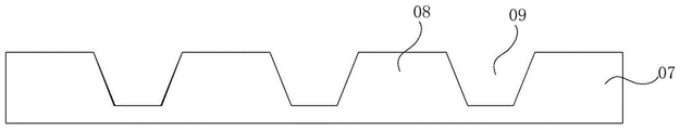
Referring to fig. 3a, a substrate is provided and an active region 08 and shallow trench isolation region 09 are formed on the substrate 07. The substrate 07 may be a polysilicon substrate. The material of the substrate 07 is not particularly limited in the present invention, and the substrate 07 may be a semiconductor substrate or a composite structure substrate. The material of the semiconductor substrate may include silicon, germanium, silicon germanium, gallium arsenide, or the like.
Referring to fig. 3b, a shallow trench oxide layer 10 is formed in the shallow trench isolation region and fills the shallow trench isolation region. Referring to fig. 3c, a first oxide layer 17, a floating gate layer 18, and a dielectric layer 19 are sequentially formed on an active region (not shown). It should be noted that fig. 3c shows a cross-sectional view of the active region, perpendicular to the cross-sectional views shown in fig. 3 a-3 b, in order to make the depicted structure more intuitive. The first oxide layer 17 is a tunnel oxide layer, and the material thereof may be silicon oxide. The dielectric layer 19 may have a thickness of And
And dielectric layer 19 may be an oxide-nitride-oxide structure.
It should be noted that, since the first oxide layer 17 and the shallow trench isolation structure are both made of oxide, silicon oxide is generally used, and the thickness of the first oxide layer 17 is small, the first oxide layer 17 may be formed on the entire substrate, so as to omit the patterning process of the first oxide layer 17 and simplify the process. The floating gate layer 18 and the dielectric layer 19 are sequentially formed in the gate region of the active region, and the floating gate structures of the memory cells are separated from each other, so that the memory cells can independently operate. In the memory cell array, control gates of the memory cells in the same row are connected through continuous control gate layers, and the continuous control gate layers are used as word lines to provide control signals for the connected memory cells and determine the working memory cells by matching with bit lines.
Referring to fig. 3d, a silicon nitride layer 31 comprising a first recess 30 is formed on the dielectric layer 19. Wherein, the silicon nitride layer 31 can be grown by using a furnace tube and has a thickness of First, the entire
 silicon nitride layer 31 is deposited, and then the first groove 30 is formed by development and dry etching.
Referring to fig. 3e, a control gate layer 11 is formed on the dielectric layer 19 exposed in the first recess and on the sidewalls and upper surface of the silicon nitride layer 31. The control gate layer 11 may be prepared by a furnace growth process, and may have a thickness of
Referring to fig. 3f, the control gate layer 11, the dielectric layer 19, the floating gate layer 18, and the first oxide layer 17 are sequentially etched to form the second groove 32. Wherein the second recess 32 corresponds to the source. And etching the control gate layer 11, the dielectric layer 19, the floating gate layer 18 and the first oxide layer 17 by adopting a dry etching process. It should be noted that the silicon nitride layer 31 belongs to a hard mask body and is not affected by the dry etching in this embodiment, the thickness of the control gate layer 11 in the first groove is relatively large, although affected by the dry etching, a part of the volume close to the silicon nitride layer 31 is still remained to form a silicon nitride polysilicon wall, and the thickness close to the silicon nitride layer is larger than the thickness far from the silicon nitride layer, compared with the prior art, the aspect ratio of the second groove 32 is reduced, the etching and cleaning difficulty of the second groove is reduced, and ion implantation is facilitated.
It should be further noted that the second groove 32 includes an active region second groove and a shallow trench isolation region second groove, which are both completed in the same etching process step, and the oxide filled in the shallow trench isolation structure corresponding to the shallow trench isolation region second groove is also removed by dry etching in the above process step, so as to prevent the oxide from blocking ion implantation performed when a source terminal conductive trench is formed in a subsequent process.
Referring to fig. 3g, a second trench recess 32 is formed in a portion of the bottom of the active region that leaks out of the source region in the active region, and the source electrode 15 is formed by an ion implantation process. Fig. 3h is a schematic view of a cross section of a NOR flash in a direction perpendicular to the shallow trench structure during the same ion implantation process as in fig. 3g, where the cross section includes only a source and a shallow trench isolation region adjacent to the source. As shown in fig. 3h, the source terminal conductive trench 21 is adjacent to the corresponding source 15, and the source 15 and the source terminal conductive trench 21 are formed by the same ion implantation, so that the thicknesses of the doped regions of the source 15 and the source terminal conductive trench 21 are the same, and the source 15 of each memory cell in the same row in the memory cell array is led out through the source terminal conductive trench 21. It should be noted that the shape of the source terminal conductive trench 21 is similar to the trench structure formed in the shallow trench isolation structure, and is generally a trapezoid, when ion implantation is performed, ions are implanted into both the bottom and the sidewall of the trapezoid, and in order to improve the electrical performance of the source terminal conductive trench 21, tilt angle implantation is typically performed on the sidewall, so that the thicknesses of the doped regions at the bottom and the sidewall of the source terminal conductive trench 21 are equal.
Referring to fig. 3i, a second oxide layer 33 is formed in the first and second grooves. It should be noted that the second oxide layer 33 is used to fill the first and second grooves, and the formed excessive second oxide layer 33 is removed by a chemical mechanical polishing process.
Referring to fig. 3j, the remaining silicon nitride layer is removed. It should be noted that the remaining silicon nitride layer corresponds to the drain electrode of the active region and the shallow trench isolation region adjacent to the drain electrode, and after removing the remaining silicon nitride layer, the surface of the dielectric layer 19 corresponding to the drain electrode is exposed, specifically, the remaining silicon nitride layer may be stripped by using phosphoric acid. In addition, since the gates of the memory cells only exist in the gate region of the active region, the dielectric layer 19, the floating gate layer 18 and the first oxide layer 17 corresponding to the drain belong to redundant structures.
Referring to fig. 3k, the excess dielectric layer 19, the excess floating gate layer 18 and the excess first oxide layer 17 are removed to form a gate. Specifically, the excess dielectric layer 19, the excess floating gate layer 18, and the excess first oxide layer 17 may be removed by etching.
Note that the second oxide layer 33 is left in this embodiment. On one hand, the second oxide layer 33 in the second groove is in direct contact with the gate and can be used as a gate oxide wall, and on the other hand, pollution and impurities caused by removing the second oxide layer 33 are avoided.
Referring to fig. 3l, the gate oxide wall 22, the drain electrode 14 and the contact window 16 are sequentially formed. The gate oxide layer wall 22 is tightly attached to the gate, is formed only on the sidewall of the gate 13, and is used for protecting the gate 13, and plays an electrical insulation role to avoid the mutual influence between the electrodes. Since the second oxide layer 33 remains, the gate oxide wall 22 may be formed only on the sidewall of the gate away from the second oxide layer 33. The drain electrode 14 is formed by an ion implantation process using the same ion electric polarity as that implanted when the source electrode is formed. A contact window 16 is formed on the drain electrode 14, and the contact surface area of the contact window with the corresponding drain electrode 14 is smaller than the area of the drain electrode 14, so as to lead out the drain electrode 14.
Compared with the traditional process, the method for manufacturing the flash memory provided by the embodiment of the invention omits the use of the photoresist, avoids the phenomenon of ion implantation blockage caused by the difficulty in cleaning the residual photoresist, reduces the depth-to-width ratio of the groove required to be obtained when the source electrode is formed, and improves the operation efficiency and reliability of the chip.
The embodiment of the invention also provides a flash memory, and the flash memory can be prepared by the manufacturing method of the flash memory provided by any embodiment of the invention.
It is to be noted that the foregoing is only illustrative of the preferred embodiments of the present invention and the technical principles employed. It will be understood by those skilled in the art that the present invention is not limited to the particular embodiments described herein, but is capable of various obvious changes, rearrangements and substitutions as will now become apparent to those skilled in the art without departing from the scope of the invention. Therefore, although the present invention has been described in greater detail by the above embodiments, the present invention is not limited to the above embodiments, and may include other equivalent embodiments without departing from the spirit of the present invention, and the scope of the present invention is determined by the scope of the appended claims.
Claims (9)
1. A method for manufacturing a flash memory, comprising:
providing a substrate, forming an active region and a shallow trench isolation region on the substrate, and sequentially forming a first oxide layer, a floating gate layer and a dielectric layer on the active region;
forming a silicon nitride layer containing a first groove on the dielectric layer;
forming a control gate layer on the dielectric layer exposed in the first groove and forming a second groove;
respectively forming source electrode and source electrode end conductive grooves on the active region exposed at the bottom of the second groove and the shallow channel isolation region adjacent to the active region;
forming a second oxide layer in the first groove and the second groove, and removing the residual silicon nitride layer, the redundant dielectric layer, the redundant floating gate layer and the redundant first oxide layer to form a gate;
sequentially forming a gate oxide layer wall, a drain electrode and a contact window;
wherein the first groove is formed by adopting a dry etching process;
wherein, form the control gate layer on the exposed dielectric layer in the said first recess, and form the second recess, include:
forming a control gate layer on the dielectric layer exposed in the first groove and on the side wall and the upper surface of the silicon nitride layer;
and etching the control gate layer, the dielectric layer, the floating gate layer and the first oxidation layer in sequence to form the second groove.
2. The method of claim 1, wherein forming source and source-side conductive trenches in the exposed active region at the bottom of the second recess and the shallow trench isolation region adjacent to the active region, respectively, comprises:
and simultaneously performing ion implantation on the active region exposed at the bottom of the second groove and the shallow trench isolation region adjacent to the active region to form the source electrode and the source electrode end conductive groove.
3. The method of claim 2 wherein the doped regions of the source and source terminal conductive trenches are of equal thickness.
4. The method of claim 1, wherein removing the remaining silicon nitride layer, the excess dielectric layer, the excess floating gate layer, and the excess first oxide layer to form a gate electrode comprises:
stripping the rest silicon nitride layer by using phosphoric acid;
and removing the redundant dielectric layer, the redundant floating gate layer and the redundant first oxide layer through etching to form the grid.
5. The method of claim 1, wherein the dielectric layer has a thickness in a range of values
6. The method of claim 1, wherein the silicon nitride layer has a thickness in a range of values
7. The method of claim 1, wherein forming a control gate layer over the dielectric layer exposed in the first recess comprises:
and forming a control gate layer on the dielectric layer exposed in the first groove by adopting a furnace tube growth process.
8. The method of claim 1, wherein the control gate layer thickness ranges from
9. A flash memory manufactured by the method of any one of claims 1 to 8.
Priority Applications (1)
| Application Number | Priority Date | Filing Date | Title |
|---|---|---|---|
| CN201610017863.9A CN106972019B (en) | 2016-01-12 | 2016-01-12 | Flash memory and manufacturing method thereof |
Applications Claiming Priority (1)
| Application Number | Priority Date | Filing Date | Title |
|---|---|---|---|
| CN201610017863.9A CN106972019B (en) | 2016-01-12 | 2016-01-12 | Flash memory and manufacturing method thereof |
Publications (2)
| Publication Number | Publication Date |
|---|---|
| CN106972019A CN106972019A (en) | 2017-07-21 |
| CN106972019B true CN106972019B (en) | 2020-03-24 |
Family
ID=59334215
Family Applications (1)
| Application Number | Title | Priority Date | Filing Date |
|---|---|---|---|
| CN201610017863.9A Active CN106972019B (en) | 2016-01-12 | 2016-01-12 | Flash memory and manufacturing method thereof |
Country Status (1)
| Country | Link |
|---|---|
| CN (1) | CN106972019B (en) |
Families Citing this family (2)
| Publication number | Priority date | Publication date | Assignee | Title |
|---|---|---|---|---|
| CN109935592B (en) * | 2019-04-16 | 2023-12-01 | 上海格易电子有限公司 | Memory and preparation method thereof |
| CN110931492A (en) * | 2019-12-09 | 2020-03-27 | 上海华力微电子有限公司 | Integrated process method of NOR flash memory |
Citations (1)
| Publication number | Priority date | Publication date | Assignee | Title |
|---|---|---|---|---|
| CN1134054C (en) * | 1996-09-04 | 2004-01-07 | 冲电气工业株式会社 | Nonvolatile semiconductor memory and fabricating method |
Family Cites Families (6)
| Publication number | Priority date | Publication date | Assignee | Title |
|---|---|---|---|---|
| TW480676B (en) * | 2001-03-28 | 2002-03-21 | Nanya Technology Corp | Manufacturing method of flash memory cell |
| US6635533B1 (en) * | 2003-03-27 | 2003-10-21 | Powerchip Semiconductor Corp. | Method of fabricating flash memory |
| KR100621553B1 (en) * | 2004-09-22 | 2006-09-19 | 삼성전자주식회사 | Nonvolatile memory device and method for fabricating the same |
| CN102130132B (en) * | 2010-01-18 | 2013-03-13 | 上海华虹Nec电子有限公司 | EEPROM (electronically erasable programmable read-only memory) device and manufacturing method thereof |
| CN101807577B (en) * | 2010-03-12 | 2015-05-27 | 上海华虹宏力半导体制造有限公司 | Split gate flash memory and manufacture method thereof |
| CN104465524B (en) * | 2014-12-30 | 2018-04-27 | 上海华虹宏力半导体制造有限公司 | Mirror image Split-gate flash memory and forming method thereof |
-
2016
- 2016-01-12 CN CN201610017863.9A patent/CN106972019B/en active Active
Patent Citations (1)
| Publication number | Priority date | Publication date | Assignee | Title |
|---|---|---|---|---|
| CN1134054C (en) * | 1996-09-04 | 2004-01-07 | 冲电气工业株式会社 | Nonvolatile semiconductor memory and fabricating method |
Also Published As
| Publication number | Publication date |
|---|---|
| CN106972019A (en) | 2017-07-21 |
Similar Documents
| Publication | Publication Date | Title |
|---|---|---|
| TWI520275B (en) | Memory device and method of manufacturing the same | |
| US7316955B2 (en) | Method of manufacturing semiconductor device | |
| KR101813820B1 (en) | Formation of self-aligned source for split-gate non-volatile memory cell | |
| KR100720232B1 (en) | Method for forming semiconductor device having fin structure | |
| US11088155B2 (en) | Method for fabricating split-gate non-volatile memory | |
| US7049189B2 (en) | Method of fabricating non-volatile memory cell adapted for integration of devices and for multiple read/write operations | |
| CN106972019B (en) | Flash memory and manufacturing method thereof | |
| KR100608507B1 (en) | Method for the production of a nrom memory cell field | |
| US20080048253A1 (en) | Semiconductor device having a recess channel structure and method for manufacturing the same | |
| KR100753038B1 (en) | Method for forming contact plug in semiconductor device | |
| JP5030047B2 (en) | Manufacturing method of semiconductor device | |
| US20120292684A1 (en) | Non-volatile memory device and method for fabricating the same | |
| KR100791331B1 (en) | Nonvolatile memory device and method for fabricating the same | |
| KR100419963B1 (en) | Method for manufacturing common source region of flash memory device | |
| KR20230031334A (en) | Split gate having erase gate disposed over word line gate, 2-bit non-volatile memory cell, and manufacturing method thereof | |
| US20060263989A1 (en) | Semiconductor device and fabrication method therefor | |
| KR20100138542A (en) | Manufacturing method of gate pattern for nonvolatile memory device | |
| TWI815380B (en) | Method of manufacturing non-volatile memory device | |
| CN108666315B (en) | Flash memory and manufacturing method thereof | |
| CN101399206A (en) | Method for making flash memory | |
| KR100680487B1 (en) | Method of forming a dielectric spacer in a NAND flash memory device | |
| KR20030049781A (en) | Method of manufacturing a flash memory cell | |
| CN106972018A (en) | A kind of flash memory and preparation method thereof | |
| KR100799056B1 (en) | Method for fabricating a semiconductor device | |
| KR100862145B1 (en) | Flash memory device and method for manufacturing the same |
Legal Events
| Date | Code | Title | Description |
|---|---|---|---|
| PB01 | Publication | ||
| SE01 | Entry into force of request for substantive examination | ||
| SE01 | Entry into force of request for substantive examination | ||
| GR01 | Patent grant | ||
| GR01 | Patent grant | ||
| CP01 | Change in the name or title of a patent holder |
Address after: 502 / 15, building 1, 498 GuoShouJing Road, Zhangjiang High Tech Park, Pudong New Area, Shanghai 201203 Patentee after: SHANGHAI GEYI ELECTRONIC Co.,Ltd. Patentee after: Zhaoyi Innovation Technology Group Co.,Ltd. Address before: 502 / 15, building 1, 498 GuoShouJing Road, Zhangjiang High Tech Park, Pudong New Area, Shanghai 201203 Patentee before: SHANGHAI GEYI ELECTRONIC Co.,Ltd. Patentee before: GIGADEVICE SEMICONDUCTOR(BEIJING) Inc. |
|
| CP01 | Change in the name or title of a patent holder |