CN106935491B - Laser annealing device and annealing method thereof - Google Patents
Laser annealing device and annealing method thereof Download PDFInfo
- Publication number
- CN106935491B CN106935491B CN201511021931.0A CN201511021931A CN106935491B CN 106935491 B CN106935491 B CN 106935491B CN 201511021931 A CN201511021931 A CN 201511021931A CN 106935491 B CN106935491 B CN 106935491B
- Authority
- CN
- China
- Prior art keywords
- laser
- annealing
- silicon wafer
- temperature
- control system
- Prior art date
- Legal status (The legal status is an assumption and is not a legal conclusion. Google has not performed a legal analysis and makes no representation as to the accuracy of the status listed.)
- Active
Links
Images


Classifications
-
- H—ELECTRICITY
- H01—ELECTRIC ELEMENTS
- H01L—SEMICONDUCTOR DEVICES NOT COVERED BY CLASS H10
- H01L21/00—Processes or apparatus adapted for the manufacture or treatment of semiconductor or solid state devices or of parts thereof
- H01L21/67—Apparatus specially adapted for handling semiconductor or electric solid state devices during manufacture or treatment thereof; Apparatus specially adapted for handling wafers during manufacture or treatment of semiconductor or electric solid state devices or components ; Apparatus not specifically provided for elsewhere
- H01L21/67005—Apparatus not specifically provided for elsewhere
- H01L21/67011—Apparatus for manufacture or treatment
- H01L21/67098—Apparatus for thermal treatment
-
- B—PERFORMING OPERATIONS; TRANSPORTING
- B23—MACHINE TOOLS; METAL-WORKING NOT OTHERWISE PROVIDED FOR
- B23K—SOLDERING OR UNSOLDERING; WELDING; CLADDING OR PLATING BY SOLDERING OR WELDING; CUTTING BY APPLYING HEAT LOCALLY, e.g. FLAME CUTTING; WORKING BY LASER BEAM
- B23K26/00—Working by laser beam, e.g. welding, cutting or boring
- B23K26/02—Positioning or observing the workpiece, e.g. with respect to the point of impact; Aligning, aiming or focusing the laser beam
- B23K26/03—Observing, e.g. monitoring, the workpiece
- B23K26/034—Observing the temperature of the workpiece
-
- B—PERFORMING OPERATIONS; TRANSPORTING
- B23—MACHINE TOOLS; METAL-WORKING NOT OTHERWISE PROVIDED FOR
- B23K—SOLDERING OR UNSOLDERING; WELDING; CLADDING OR PLATING BY SOLDERING OR WELDING; CUTTING BY APPLYING HEAT LOCALLY, e.g. FLAME CUTTING; WORKING BY LASER BEAM
- B23K26/00—Working by laser beam, e.g. welding, cutting or boring
- B23K26/0006—Working by laser beam, e.g. welding, cutting or boring taking account of the properties of the material involved
-
- B—PERFORMING OPERATIONS; TRANSPORTING
- B23—MACHINE TOOLS; METAL-WORKING NOT OTHERWISE PROVIDED FOR
- B23K—SOLDERING OR UNSOLDERING; WELDING; CLADDING OR PLATING BY SOLDERING OR WELDING; CUTTING BY APPLYING HEAT LOCALLY, e.g. FLAME CUTTING; WORKING BY LASER BEAM
- B23K26/00—Working by laser beam, e.g. welding, cutting or boring
- B23K26/02—Positioning or observing the workpiece, e.g. with respect to the point of impact; Aligning, aiming or focusing the laser beam
- B23K26/06—Shaping the laser beam, e.g. by masks or multi-focusing
- B23K26/064—Shaping the laser beam, e.g. by masks or multi-focusing by means of optical elements, e.g. lenses, mirrors or prisms
- B23K26/0648—Shaping the laser beam, e.g. by masks or multi-focusing by means of optical elements, e.g. lenses, mirrors or prisms comprising lenses
-
- H—ELECTRICITY
- H01—ELECTRIC ELEMENTS
- H01L—SEMICONDUCTOR DEVICES NOT COVERED BY CLASS H10
- H01L21/00—Processes or apparatus adapted for the manufacture or treatment of semiconductor or solid state devices or of parts thereof
- H01L21/02—Manufacture or treatment of semiconductor devices or of parts thereof
- H01L21/04—Manufacture or treatment of semiconductor devices or of parts thereof the devices having at least one potential-jump barrier or surface barrier, e.g. PN junction, depletion layer or carrier concentration layer
- H01L21/18—Manufacture or treatment of semiconductor devices or of parts thereof the devices having at least one potential-jump barrier or surface barrier, e.g. PN junction, depletion layer or carrier concentration layer the devices having semiconductor bodies comprising elements of Group IV of the Periodic System or AIIIBV compounds with or without impurities, e.g. doping materials
- H01L21/26—Bombardment with radiation
- H01L21/263—Bombardment with radiation with high-energy radiation
- H01L21/268—Bombardment with radiation with high-energy radiation using electromagnetic radiation, e.g. laser radiation
-
- H—ELECTRICITY
- H01—ELECTRIC ELEMENTS
- H01L—SEMICONDUCTOR DEVICES NOT COVERED BY CLASS H10
- H01L21/00—Processes or apparatus adapted for the manufacture or treatment of semiconductor or solid state devices or of parts thereof
- H01L21/02—Manufacture or treatment of semiconductor devices or of parts thereof
- H01L21/04—Manufacture or treatment of semiconductor devices or of parts thereof the devices having at least one potential-jump barrier or surface barrier, e.g. PN junction, depletion layer or carrier concentration layer
- H01L21/18—Manufacture or treatment of semiconductor devices or of parts thereof the devices having at least one potential-jump barrier or surface barrier, e.g. PN junction, depletion layer or carrier concentration layer the devices having semiconductor bodies comprising elements of Group IV of the Periodic System or AIIIBV compounds with or without impurities, e.g. doping materials
- H01L21/30—Treatment of semiconductor bodies using processes or apparatus not provided for in groups H01L21/20 - H01L21/26
- H01L21/324—Thermal treatment for modifying the properties of semiconductor bodies, e.g. annealing, sintering
-
- H—ELECTRICITY
- H01—ELECTRIC ELEMENTS
- H01L—SEMICONDUCTOR DEVICES NOT COVERED BY CLASS H10
- H01L21/00—Processes or apparatus adapted for the manufacture or treatment of semiconductor or solid state devices or of parts thereof
- H01L21/67—Apparatus specially adapted for handling semiconductor or electric solid state devices during manufacture or treatment thereof; Apparatus specially adapted for handling wafers during manufacture or treatment of semiconductor or electric solid state devices or components ; Apparatus not specifically provided for elsewhere
- H01L21/67005—Apparatus not specifically provided for elsewhere
- H01L21/67242—Apparatus for monitoring, sorting or marking
- H01L21/67248—Temperature monitoring
-
- H—ELECTRICITY
- H01—ELECTRIC ELEMENTS
- H01S—DEVICES USING THE PROCESS OF LIGHT AMPLIFICATION BY STIMULATED EMISSION OF RADIATION [LASER] TO AMPLIFY OR GENERATE LIGHT; DEVICES USING STIMULATED EMISSION OF ELECTROMAGNETIC RADIATION IN WAVE RANGES OTHER THAN OPTICAL
- H01S3/00—Lasers, i.e. devices using stimulated emission of electromagnetic radiation in the infrared, visible or ultraviolet wave range
- H01S3/05—Construction or shape of optical resonators; Accommodation of active medium therein; Shape of active medium
- H01S3/06—Construction or shape of active medium
- H01S3/063—Waveguide lasers, i.e. whereby the dimensions of the waveguide are of the order of the light wavelength
- H01S3/067—Fibre lasers
-
- H—ELECTRICITY
- H01—ELECTRIC ELEMENTS
- H01S—DEVICES USING THE PROCESS OF LIGHT AMPLIFICATION BY STIMULATED EMISSION OF RADIATION [LASER] TO AMPLIFY OR GENERATE LIGHT; DEVICES USING STIMULATED EMISSION OF ELECTROMAGNETIC RADIATION IN WAVE RANGES OTHER THAN OPTICAL
- H01S3/00—Lasers, i.e. devices using stimulated emission of electromagnetic radiation in the infrared, visible or ultraviolet wave range
- H01S3/10—Controlling the intensity, frequency, phase, polarisation or direction of the emitted radiation, e.g. switching, gating, modulating or demodulating
- H01S3/13—Stabilisation of laser output parameters, e.g. frequency or amplitude
-
- H—ELECTRICITY
- H01—ELECTRIC ELEMENTS
- H01S—DEVICES USING THE PROCESS OF LIGHT AMPLIFICATION BY STIMULATED EMISSION OF RADIATION [LASER] TO AMPLIFY OR GENERATE LIGHT; DEVICES USING STIMULATED EMISSION OF ELECTROMAGNETIC RADIATION IN WAVE RANGES OTHER THAN OPTICAL
- H01S3/00—Lasers, i.e. devices using stimulated emission of electromagnetic radiation in the infrared, visible or ultraviolet wave range
- H01S3/23—Arrangements of two or more lasers not provided for in groups H01S3/02 - H01S3/22, e.g. tandem arrangements of separate active media
-
- B—PERFORMING OPERATIONS; TRANSPORTING
- B23—MACHINE TOOLS; METAL-WORKING NOT OTHERWISE PROVIDED FOR
- B23K—SOLDERING OR UNSOLDERING; WELDING; CLADDING OR PLATING BY SOLDERING OR WELDING; CUTTING BY APPLYING HEAT LOCALLY, e.g. FLAME CUTTING; WORKING BY LASER BEAM
- B23K2103/00—Materials to be soldered, welded or cut
- B23K2103/50—Inorganic material, e.g. metals, not provided for in B23K2103/02 – B23K2103/26
- B23K2103/56—Inorganic material, e.g. metals, not provided for in B23K2103/02 – B23K2103/26 semiconducting
-
- H—ELECTRICITY
- H01—ELECTRIC ELEMENTS
- H01L—SEMICONDUCTOR DEVICES NOT COVERED BY CLASS H10
- H01L21/00—Processes or apparatus adapted for the manufacture or treatment of semiconductor or solid state devices or of parts thereof
- H01L21/02—Manufacture or treatment of semiconductor devices or of parts thereof
- H01L21/02104—Forming layers
- H01L21/02365—Forming inorganic semiconducting materials on a substrate
- H01L21/02656—Special treatments
- H01L21/02664—Aftertreatments
- H01L21/02667—Crystallisation or recrystallisation of non-monocrystalline semiconductor materials, e.g. regrowth
- H01L21/02675—Crystallisation or recrystallisation of non-monocrystalline semiconductor materials, e.g. regrowth using laser beams
- H01L21/02678—Beam shaping, e.g. using a mask
-
- H—ELECTRICITY
- H01—ELECTRIC ELEMENTS
- H01L—SEMICONDUCTOR DEVICES NOT COVERED BY CLASS H10
- H01L21/00—Processes or apparatus adapted for the manufacture or treatment of semiconductor or solid state devices or of parts thereof
- H01L21/02—Manufacture or treatment of semiconductor devices or of parts thereof
- H01L21/02104—Forming layers
- H01L21/02365—Forming inorganic semiconducting materials on a substrate
- H01L21/02656—Special treatments
- H01L21/02664—Aftertreatments
- H01L21/02667—Crystallisation or recrystallisation of non-monocrystalline semiconductor materials, e.g. regrowth
- H01L21/02691—Scanning of a beam
Abstract
The invention discloses a laser annealing device and an annealing method thereof, wherein the laser annealing device comprises a laser light source system, a laser adjusting system connected with the laser light source system and positioned above a silicon wafer, a temperature monitoring system positioned above the silicon wafer and used for measuring the temperature of a light spot position on the surface of the silicon wafer in real time, and a central control system respectively connected with the laser light source system, the laser adjusting system, the temperature monitoring system and a wafer carrying platform. According to the invention, the plurality of independent lasers are arranged to provide lasers with different wavelengths, the silicon wafer is subjected to combined annealing, the silicon wafer is annealed by selecting the optimal process parameter group, and the lasers with different wavelengths are complemented, so that the optimal annealing temperature is reached, and the image effect on the surface of the silicon wafer is well inhibited; through a feedback mechanism of the temperature monitoring system and an adjusting mechanism of the central control system, the uniformity and controllability of annealing are improved, the thermal budget is reduced, the thermal diffusion is reduced, and the process adaptability of the annealing device is improved.
Description
Technical Field
The invention relates to the technical field of laser annealing, in particular to a laser annealing device and an annealing method thereof.
Background
In the manufacture of a semiconductor device, when ion implantation is performed in a predetermined region on the back surface of a silicon substrate, P ions are generally implanted in a deep layer, and B ions are generally implanted in a shallow layer, and the solubility of the B ions is higher than that of the P ions in the deep layer. In view of the above problems, a laser annealing method is generally used for a semiconductor film formed on an insulating substrate such as glass to achieve crystallization or increase crystallinity, and as a result of the laser annealing, an amorphous material is converted into a polycrystalline or single crystalline state, and after ion implantation, doped impurities are combined with an ordered arrangement of atoms in the crystal, thereby effectively improving electrical characteristics of the material.
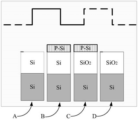
After a silicon wafer is subjected to a photolithography process, such as a TSV (through silicon via) technique, different nm-level geometric structures and material properties are formed at different positions of a surface, which causes inconsistent absorption of incident laser energy at different positions of the surface, and thus causes a deterioration in uniformity of temperature distribution on the surface after laser annealing, i.e., a so-called pattern effect.
As shown in fig. 1, it is a schematic structural diagram of a silicon wafer surface after being processed by a specific photolithography process. It can be seen that the silicon wafer surface is comprised of a series of bare chips 1' shown as black boxes. For the formed die 1', a series of specific periodic structures with spatial dimensions on the nm scale on the surface and different material compositions are shown in fig. 2. Therefore, the reflectance R (x, y) of the upper surface of the silicon wafer with respect to incident light differs depending on the position.
Meanwhile, according to the electromagnetic wave theory, the reflectivity R (λ, θ) of a specific material surface is a function of the wavelength λ of incident light and the incident angle θ. For laser with specific wavelength, the reflectivity R of the surface of the silicon wafer is obtained when the laser is incident at different incidence anglesλ(θ) varies with the incident angle, and as shown in fig. 3a and 3b, the reflectivity of the laser beams with 800nm and 500nm incident on A, B, C, D shown in fig. 2 is plotted with the incident angle. It can be found that the reflectance R is the same for incident light of the same wavelengthλ(θ) varies with the angle of incidence; while the reflectivity R is the same for the same incident angleθ(λ) may also vary with the wavelength of the incident light.
In summary, for a silicon wafer processed by a photolithography process, the reflectivity R (λ, θ, x, y) of incident light is related to the surface position of the silicon wafer, the wavelength of the laser used and the incident angle.
The existing laser annealing technology uses laser as an energy source to irradiate the surface of a silicon wafer to be processed, so that the surface of the silicon wafer reaches a specified annealing temperature T0, and the target annealing is realized. However, the existing laser annealing technology only adopts a laser with one wavelength for annealing, and inevitably causes the problem of silicon wafer surface pattern effect, which can generate important influence on the consistency of device performance, thereby reducing the photoetching effect and stability of the silicon wafer.
Disclosure of Invention
The invention provides a laser annealing device and an annealing method thereof, which aim to solve the technical problems.
In order to solve the technical problems, the technical scheme of the invention is as follows: a laser annealing device is used for carrying out laser annealing on a silicon wafer on a wafer carrying table and comprises:
the laser light source system comprises at least two lasers and outputs laser beams, and the power of the laser beams is adjustable;
the laser adjusting system is connected with the laser light source system, is positioned above the silicon wafer, comprises at least two laser adjusters which correspond to the lasers one by one, monitors the power of the corresponding laser beams and the positions of light spots on the surface of the silicon wafer, and adjusts the shapes and the incident angles of the light spots;
the temperature monitoring system is positioned above the silicon wafer and is used for measuring the temperature of the light spot position on the surface of the silicon wafer in real time;
and the central control system is respectively connected with the laser light source system, the laser adjusting system, the temperature monitoring system and the slide holder, receives the data information of the laser light source system, the laser adjusting system, the temperature monitoring system and the slide holder and controls the laser light source system, the laser adjusting system and the slide holder.
Furthermore, a laser light source control system is connected between the central control system and the laser light source system, receives a control command of the central control system to control the power of the laser beam output by each laser in the laser light source system, and feeds back a control result to the central control system.
Furthermore, a laser regulation control system is connected between the central control system and the laser regulation system, receives a control command of the central control system to control each laser regulator in the laser regulation system, and feeds back a control result to the central control system.
Furthermore, a slide holder control system is arranged between the central control system and the slide holder, receives a control command of the central control system to control the movement of the slide holder, and feeds back a control result to the central control system.
Further, the temperature monitoring system is a pyrometer or a reflectivity detector.
Further, the laser and the laser regulator are connected through an optical fiber.
Furthermore, each laser regulator comprises a light spot detection system, an energy attenuation system, a light homogenizing system and a rotating and displacing device which are arranged along a light path, wherein the light spot detection system is respectively connected with the laser and the central processing system, and the rotating and displacing device is positioned above the silicon wafer.
Further, the light spot detection system comprises a power meter, a CCD detector and an image collector.
Further, the dodging system adopts a micro-lens array or an optical integrating rod.
Furthermore, a beam expanding and collimating system is arranged between the energy attenuation system and the light homogenizing system, collimates the light beam and controls the shape of the light spot.
Further, the rotating and displacing device comprises a galvanometer lens and a piezoelectric ceramic displacing device.
Furthermore, an F-theta lens is arranged between the rotating and displacing device and the silicon wafer.
The invention also provides an annealing method of the laser annealing device, which comprises the following steps:
s1: placing the silicon wafer on a wafer carrying platform to complete the posture adjustment of the silicon wafer along the horizontal direction;
s2: determining the position of a light spot in the silicon wafer according to the position of a laser regulator in a laser regulation system, and selecting the optimal process parameter set according to the reflectivity of the position of the light spot;
s3: adjusting a laser light source system and a laser adjusting system, exposing the light spot position by adopting the optimal process parameters, measuring temperature data at the light spot position by a temperature monitoring system, and sending the temperature data to a central control system;
s4: the central control system judges whether the temperature meets the set temperature range according to the received temperature data; if not, recording the exposure temperature at the position, and adjusting the parameters of the laser light source system and the laser adjusting system when exposing the next silicon wafer position with the same reflectivity to ensure that the exposure temperature is in a set range; if so, controlling the wafer carrying platform to drive the silicon wafer to move to the next exposure position relative to the light spot;
s5: and judging whether the position is an end position, if not, repeating the steps S2-S4, and if not, ending.
Further, in step S2, the selecting the optimal set of process parameters includes the following steps:
s21: selecting the wavelength of each laser;
s22: aiming at any position on the silicon chip, adjusting the incident angle and the power of each laser to form a plurality of parameter combinations comprising the incident angle and the laser power of each laser;
s23: selecting one parameter combination, measuring the reflectivity and the absorbed light intensity of the position of the silicon wafer to the laser beams corresponding to the lasers, and obtaining the exposure temperature corresponding to the parameter combination through a temperature model;
s24: judging whether the exposure temperature meets a set temperature range or not; and if not, selecting the next group of parameter combinations, jumping to the step S23, if so, determining the group of parameter combinations as the optimal process parameter group, moving the slide holder to the next position of the silicon wafer, and jumping to the step S23 until all positions on the silicon wafer 1 are traversed.
The invention also provides an annealing method of the laser annealing device, which comprises the following steps:
s1: arranging a silicon wafer on a wafer bearing table to obtain process parameters of the surface of the silicon wafer;
s2: selecting at least 2 lasers to generate laser beams according to the process parameters, and adjusting different annealing angles and different annealing powers through corresponding laser regulators;
s3: and integrating the laser beams into annealing light spots to carry out a silicon wafer surface annealing process.
Further, in step S1, the process parameters are obtained by selecting from parameter models obtained by measuring the surface type of the silicon wafer in advance during the annealing process according to the type of the silicon wafer.
Further, in step S1, the process parameters are obtained by measuring the surface profile of the silicon wafer in real time during the annealing process.
Further, the process parameters include surface profile distribution of the silicon wafer surface and reflectivity of the material.
Further, in step S2, at least 2 laser beams with different wavelengths are selected according to the reflectivity of the material, and the power of the laser beams is adjusted by the corresponding laser regulators.
Further, in step S2, the incident angle of the laser beam is adjusted by the corresponding laser adjuster according to the surface profile of the surface, so as to obtain different annealing angles.
Further, in step S3, the energy distribution of the annealing spot is matched with the surface profile of the silicon wafer surface and the reflectivity of the material.
The invention provides a laser annealing device and an annealing method thereof, wherein a plurality of independent lasers are arranged to provide lasers with different wavelengths, a silicon wafer is subjected to combined annealing, the silicon wafer is annealed by selecting an optimal process parameter group, and the lasers with different wavelengths are complemented, so that the optimal annealing temperature is achieved, and the image effect on the surface of the silicon wafer is well inhibited; through a feedback mechanism of the temperature monitoring system and an adjusting mechanism of the central control system, the uniformity and controllability of annealing are improved, the thermal budget is reduced, the thermal diffusion is reduced, and the process adaptability of the annealing device is improved.
Drawings
FIG. 1 is a schematic structural view of a prior art silicon wafer surface;
FIG. 2 is a schematic view of the internal structure of a prior art silicon wafer;
FIGS. 3a and 3b are graphs showing the reflectivity of laser light with a wavelength of 800nm and a wavelength of 500nm incident on A, B, C, D of FIG. 2 according to the incident angle;
FIG. 4 is a schematic structural view of a laser annealing apparatus according to the present invention;
FIG. 5 is a schematic diagram of the construction of the laser regulator of the present invention;
FIG. 6 is a schematic diagram of the spots formed by 3 different lasers incident on the surface of a silicon wafer;
FIG. 7 is a graph of temperature difference changes from annealing for different sets of process parameters for laser formation at two wavelengths, 500nm and 800 nm.
Shown in FIG. 1: 1', a bare chip;
shown in FIGS. 4-7: 1. a silicon wafer; 2. a slide stage; 3. a laser light source system; 31. a laser; 4. a laser regulation system; 41. a laser regulator; 411. a light spot detection system; 412. an energy attenuation system; 413. a light uniformizing system; 414. a rotation and displacement device; 415. a beam expanding collimation system; 416. an F-theta lens; 5. a temperature monitoring system; 6. a central control system; 7. an optical fiber; 8. a laser light source control system; 9. a laser regulation control system; 10. slide holder control system.
Detailed Description
The invention is described in detail below with reference to the attached drawing figures:
as shown in fig. 4, the present invention provides a laser annealing apparatus for laser annealing a silicon wafer 1 on a stage 2, comprising:
the laser light source system 3 comprises at least two lasers 31, outputs laser beams, irradiates the surface of the silicon wafer 1 to anneal the silicon wafer, the power of the laser beams is adjustable, the laser wavelength output by each laser 31 is different, and the power of each laser 31 can be independently adjusted.
And the laser adjusting system 4 is connected with the laser light source system 3, is positioned above the silicon wafer 1, comprises at least two laser adjusters 41 which correspond to the lasers 31 one by one, monitors the power of the corresponding laser beams and the positions of the light spots on the surface of the silicon wafer 1, and adjusts the shapes and the incidence angles of the light spots. Preferably, the laser adjusting system 4 is connected with the laser light source system 3 through an optical fiber 7 for guiding the laser beam.
The temperature monitoring system 5 is positioned above the silicon chip 1 and is used for measuring the temperature of the light spot position on the surface of the silicon chip in real time; preferably, the temperature monitoring system 5 adopts a pyrometer or a reflectivity detector to realize real-time measurement of the temperature of the surface of the silicon wafer at the position of the light spot, and feeds back the real-time measured temperature data to the central control system 6 as a basis for feedback control.
And the central control system 6 is respectively connected with the laser light source system 3, the laser adjusting system 4, the temperature monitoring system 5 and the slide stage 2, receives the data information of the laser light source system 3, the laser adjusting system 4, the temperature monitoring system 5 and the slide stage 2, and controls the laser light source system 3, the laser adjusting system 4 and the slide stage 2. Specifically, after processing the temperature data measured by the temperature monitoring system 5, the central control system 6 feeds back the temperature data to two control degrees of freedom of the power and the incident angle of the laser beam in the laser light source system 3 and the laser adjusting system 4 in real time, so that the temperature of the surface of the silicon wafer at the position of a light spot is always kept within a set temperature range in the annealing process of the whole device, wherein the set temperature range is T0+. DELTA.T where T0At is the target annealing temperature for the wafer surface at the spot location, at is the acceptable temperature difference.
As shown in fig. 5, each of the laser regulators 41 includes a light spot detection system 411, an energy attenuation system 412, a dodging system 413, and a rotation and displacement device 414 arranged along the optical path, the light spot detection system 411 is respectively connected with the laser 31 and the central processing system 6, and includes a power meter, a CCD detector, and an image collector for monitoring the power of the laser beam in real time and transmitting the data to the central control system 6. The energy attenuation system 412 is composed of a polarization beam splitter prism and an attenuation sheet or a wave plate, and adjusts the energy of the laser beam incident to the surface of the silicon wafer in a mode of changing the transmittance or the polarization direction of the lens; the light homogenizing system 413 adopts a micro-lens array or an optical integrating rod and is used for enabling light spots incident to the surface of the silicon wafer to have specific light intensity distribution, the rotating and displacing device 414 comprises a galvanometer lens and a piezoelectric ceramic displacing device and is positioned above the silicon wafer 1, and the incident angle of laser beams incident to the surface of the silicon wafer is changed and the position of the light spots relative to the surface of the silicon wafer is changed through rotation and translation.
Referring to fig. 5, a beam expanding and collimating system 415 is further disposed between the energy attenuation system 412 and the light homogenizing system 413, and may adopt a single lens or a telescope system to collimate the laser beam and adjust the shape of the spot irradiated on the surface of the silicon wafer. Preferably, an F-theta lens 416 is further disposed between the rotating and displacing device 414 and the silicon wafer 1, so that the laser beam forms a spot with a certain energy distribution on the surface of the silicon wafer. As shown in fig. 6, there are schematic views of the spots formed by 3 different lasers 31 incident on the surface of the silicon wafer. In general, during laser annealing, the shape of the spot has a linear distribution, i.e., it is narrower in the scanning direction and longer in the non-scanning direction. The multiple light spots output by the laser adjusting system can be overlapped or partially overlapped in space. In general, the intensity energy satisfies a certain distribution in the scanning direction, while the intensity energy is uniformly distributed in the non-scanning direction.
Referring to fig. 4, a laser light source control system 8 is connected between the central control system 6 and the laser light source system 3, receives a control command from the central control system 6 to control the power of the laser beam output by each laser 31 in the laser light source system 3 so as to meet a specified power requirement, and feeds back a control result to the central control system 6, and simultaneously each laser 31 in the laser light source system 3 can send the wavelength and power information of the current laser beam to the central control system 6 through the laser light source control system 8.
Referring to fig. 4, a laser adjustment control system 9 is connected between the central control system 6 and the laser adjustment system 4, and receives a control command from the central control system 6 to control each laser adjuster 41 in the laser adjustment system 4, so that the output laser beam meets the requirements of the specified incident angle and shape, and the control result is fed back to the central control system 6.
Preferably, a slide holder control system 10 is arranged between the central control system 6 and the slide holder 2, receives a control command of the central control system 6 to control the movement of the slide holder 2, and feeds back a control result to the central control system 6. Specifically, the slide holder 2 comprises a moving table which at least freely moves in the horizontal plane, and can drive the silicon wafer 1 to move relative to the light spots, so that the light spots anneal each position on the surface of the silicon wafer, and certainly, the silicon wafer 1 needs to be within the focal depth of the laser light source system 3.
The invention also provides an annealing method of the laser annealing device, which comprises the following steps:
s1: the silicon chip 1 is placed on the chip carrying platform 2, and the posture of the silicon chip 1 along the horizontal direction is adjusted, namely the silicon chip 1 is in the horizontal state.
S2: determining Spot (x, y) position in the silicon chip 1 according to the position of the laser regulator 41 in the laser regulating system 4, and selecting the optimal process parameter set according to the reflectivity R (x, y) at the Spot position Wherein
 Corresponding to the Nth wavelength as lambdaNAt theta of laser 31NThe intensity of the laser light upon incidence; specifically, the position of the light spot irradiated on the surface of the silicon wafer can be obtained according to the relative position of the rotating and displacing
 device 414 in the laser regulator 41 and the silicon wafer 1. The selection of the optimal process parameter set specifically comprises the following steps:
s21: the wavelength λ of each laser 31 is selectedi,i=1,2…N;
S22: adjusting the incident angle and power of each laser 31 for any position (x, y) on the silicon wafer 1 to form m parameter combinations including the incident angle and laser power of each laser 31, wherein the maximum value of the laser power is the rated power of the laser 31, the incident angle Is 0 to 90 degrees;
s23: selecting one of the parameter combinations, measuringReflectivity of the corresponding laser beam for each laser 31 at (x, y) on the silicon wafer 1 And the intensity of the absorbed light
 i is 1,2, … N, and the exposure temperature T corresponding to the parameter combination is obtained through a temperature modelm;
S24: determining the exposure temperature TmWhether the set temperature range T is satisfied0+ -Delta T; if not, selecting the next group of parameter combinations, jumping to step S23, if so, determining the group of parameter combinations as the optimal process parameter group And moving the
 slide holder 2 to the next position of the silicon chip 1, and jumping to the step S23 until all positions on the silicon chip 1 are traversed.
S3: the laser light source system 3 and the laser adjusting system 4 are adjusted through the laser light source control system 8 and the laser adjusting control system 9 respectively, the optimal process parameters are adopted to expose the light spot position, meanwhile, the temperature data at the light spot position is measured through the temperature monitoring system 5, and the temperature data are sent to the central control system 6;
s4: the central control system 6 judges whether the temperature meets the set temperature range T according to the received temperature data0Within ± Δ T; if the position is not satisfied, recording the exposure temperature T (x, y) at the position, and when the next position with the same reflectivity is exposed, the central control system 6 respectively adjusts the laser light source system 3 through the laser light source control system 8 according to the exposure temperature T (x, y), and adjusts the parameters of the laser adjustment system 4 through the laser adjustment control system 9, including the incident angle and the power of the laser beam, so that the exposure temperature at the position is in a set range; if the exposure position is met, the central control system 6 controls the slide holder 2 through the slide holder control system 10 to drive the silicon wafer 1 to move to the next exposure position relative to the light spot;
s5: and judging whether the position is an end position, if not, repeating the steps S2-S4, and if not, ending.
As shown in fig. 7, annealing with a set of process parameters close to 4500 for both 500nm and 800nm wavelengths is shown, resulting in a temperature difference Δ T that varies with the process parameters, where the maximum value of the temperature difference Δ T reaches 350 ℃ and the minimum value is 110 ℃, thus demonstrating that the annealing method herein is an effective and feasible method for suppressing the pattern effect.
The invention also provides an annealing method of the laser annealing device, which comprises the following steps:
s1: arranging a silicon wafer 1 on a wafer carrying platform 2 to obtain process parameters of the surface of the silicon wafer 1; the process parameters comprise the surface profile distribution of the surface of the silicon wafer and the reflectivity of the material. The process parameters can be selected from a parameter model obtained by measuring the surface shape of the silicon wafer in advance according to the model of the silicon wafer 1 in the annealing process, or can be obtained by measuring the surface shape of the silicon wafer in real time in the annealing process.
S2: according to the process parameters, at least 2 lasers 31 are selected to provide laser beams, and different annealing angles and different annealing powers are adjusted through the laser adjusting system 4; specifically, at least 2 laser beams having different wavelengths are selected according to the reflectivity of the material, and the laser beam power is adjusted by the corresponding laser adjuster 41. Meanwhile, according to the surface profile distribution of the surface, the incident angle of the laser beam is adjusted by the rotating and shifting device 414, so as to obtain different annealing angles.
S3: and integrating the laser beams into annealing light spots, and performing a silicon wafer surface annealing process, wherein the energy distribution of the annealing light spots is matched with the surface profile distribution of the silicon wafer surface and the reflectivity of the material.
In summary, the invention provides a laser annealing device and an annealing method thereof, wherein a plurality of independent lasers 31 are arranged to provide lasers with different wavelengths, the silicon wafer 1 is jointly annealed, the silicon wafer 1 is annealed by selecting the optimal process parameter group, and the laser beams with different wavelengths are complemented, so that the optimal annealing temperature is achieved, and the pattern effect on the surface of the silicon wafer is well inhibited; through the feedback mechanism of the temperature monitoring system 5 and the adjusting mechanism of the central control system 6, the uniformity and controllability of annealing are improved, the thermal budget is reduced, the thermal diffusion is reduced, and the process adaptability of the annealing device is improved.
Although the embodiments of the present invention have been described in the specification, these embodiments are merely provided as a hint, and should not limit the scope of the present invention. Various omissions, substitutions, and changes may be made without departing from the spirit of the invention and are intended to be within the scope of the invention.
Claims (21)
1. A laser annealing device is used for carrying out laser annealing on a silicon wafer on a wafer carrying table, and is characterized by comprising:
the laser light source system comprises at least two lasers and outputs laser beams, and the power of the laser beams is adjustable;
the laser adjusting system is connected with the laser light source system, comprises at least two laser adjusters which correspond to the lasers one by one, monitors the power of the corresponding laser beams and the positions of light spots on the surface of the silicon wafer, and adjusts the shapes and the incident angles of the light spots;
the temperature monitoring system is used for measuring the temperature of the light spot position on the surface of the silicon wafer in real time;
and
and the central control system is respectively connected with the laser light source system, the laser adjusting system, the temperature monitoring system and the slide holder, receives the data information of the laser light source system, the laser adjusting system, the temperature monitoring system and the slide holder, and controls the laser light source system, the laser adjusting system and the slide holder to adjust the power and the incident angle of the laser beam output by each laser, so that the temperature of the surface of the silicon wafer at the position of the light spot is kept within a set temperature range under the simultaneous irradiation of the laser beam output by each laser in the annealing process.
2. The laser annealing device of claim 1, wherein a laser light source control system is connected between the central control system and the laser light source system, receives a control command from the central control system to control the power of the laser beam output by each laser in the laser light source system, and feeds back the control result to the central control system.
3. The laser annealing device of claim 1, wherein a laser regulation control system is connected between the central control system and the laser regulation system, and receives a control command from the central control system to control each laser regulator in the laser regulation system and feed back a control result to the central control system.
4. The laser annealing device of claim 1, wherein a stage control system is provided between the central control system and the stage, receives the control command from the central control system to control the movement of the stage, and feeds back the control result to the central control system.
5. The laser annealing device of claim 1, wherein the temperature monitoring system is a pyrometer or a reflectivity detector.
6. The laser annealing device of claim 1, wherein the laser and the laser regulator are connected by an optical fiber.
7. The laser annealing device of claim 1, wherein each laser regulator comprises a spot detection system, an energy attenuation system, a dodging system, a rotation and displacement device arranged along the optical path, the spot detection system is connected with the laser and the central processing system respectively, and the rotation and displacement device is positioned above the silicon wafer.
8. The laser annealing device of claim 7, wherein the spot detection system comprises a power meter, a CCD detector and an image collector.
9. The laser annealing device of claim 7, wherein the dodging system employs a microlens array or an optical integrator rod.
10. The laser annealing device of claim 7, wherein a beam expanding and collimating system is further disposed between the energy attenuation system and the dodging system.
11. The laser annealer of claim 7 wherein the rotation and displacement device comprises a galvanometer lens and a piezo ceramic displacement device.
12. The laser annealing device according to claim 7, wherein an F-theta lens is further provided between the rotating and displacing means and the silicon wafer.
13. An annealing method of a laser annealing device is characterized by comprising the following steps:
s1: placing a silicon wafer on a wafer carrying platform, and carrying out posture adjustment on the silicon wafer along the horizontal direction;
s2: determining the position of a light spot in the silicon wafer according to the position of a laser regulator in a laser regulation system, and selecting the optimal process parameter set according to the reflectivity of the position of the light spot;
s3: adjusting a laser adjusting system to adjust at least two lasers of a laser light source system, exposing the position of a light spot by adopting optimal process parameters, measuring temperature data of the position of the light spot by a temperature monitoring system, and sending the temperature data to a central control system; the optimal process parameters refer to the incident angle and the power of each laser when the exposure temperature at the position of a light spot meets a set temperature range;
s4: the central control system judges whether the temperature meets the set temperature range according to the received temperature data; if not, recording the exposure temperature at the position, and adjusting the parameters of the laser light source system and the laser adjusting system when exposing the next silicon wafer position with the same reflectivity to ensure that the exposure temperature is in a set range; if so, controlling the wafer carrying platform to drive the silicon wafer to move to the next exposure position relative to the light spot;
s5: and judging whether the position is an end position, if not, repeating the steps S2-S4, and if not, ending.
14. The annealing method of claim 13, wherein in step S2, the step of selecting the optimal set of process parameters comprises the steps of:
s21: selecting the wavelength of each laser;
s22: aiming at any position on the silicon chip, adjusting the incident angle and the power of each laser to form a plurality of parameter combinations comprising the incident angle and the laser power of each laser;
s23: selecting one parameter combination, measuring the reflectivity and the absorbed light intensity of the position of the silicon wafer to the laser beams corresponding to the lasers, and obtaining the exposure temperature corresponding to the parameter combination through a temperature model;
s24: judging whether the exposure temperature meets a set temperature range or not; if not, selecting the next group of parameter combinations, jumping to step S23, if yes, determining the group of parameter combinations as the best process parameter group, moving the slide holder to the next position of the silicon chip, and jumping to step S23 until all positions on the silicon chip are traversed.
15. An annealing method of a laser annealing device is characterized by comprising the following steps:
s1: setting a silicon wafer on a wafer carrying table to obtain process parameters of the surface of the silicon wafer;
s2: selecting at least 2 lasers to generate laser beams according to the process parameters, and adjusting different annealing angles and different annealing powers through corresponding laser regulators;
s3: and simultaneously irradiating the silicon wafer by using the at least two laser beams, integrating the laser beams into annealing light spots, enabling the temperature of the surface of the silicon wafer at the annealing light spots to meet a set temperature range, and carrying out a silicon wafer surface annealing process.
16. The annealing method of a laser annealing apparatus according to claim 15, wherein in step S1, the process parameter is selected from a parametric model obtained by previously measuring the surface type of the silicon wafer according to the type of the silicon wafer during the annealing process.
17. The annealing method of a laser annealer according to claim 15, wherein in step S1, said process parameters are obtained by measuring the surface profile of the silicon wafer in real time during the annealing process.
18. The annealing method of a laser annealing apparatus according to claim 15, 16 or 17, wherein the process parameters include a profile of the surface of the silicon wafer and a reflectivity of the material.
19. The annealing method of claim 18, wherein in step S2, at least 2 laser beams with different wavelengths are selected according to the reflectivity of the material, and the power of the laser beams is adjusted by the corresponding laser adjuster.
20. The annealing method of a laser annealer according to claim 19, wherein in step S2, the laser beam is adjusted by the corresponding laser adjuster to obtain different annealing angles according to the profile of the surface.
21. The annealing method of a laser annealing apparatus according to claim 18, wherein in step S3, the energy distribution of the annealing spot is matched with the profile distribution of the silicon wafer surface and the reflectance of the material.
Priority Applications (7)
| Application Number | Priority Date | Filing Date | Title |
|---|---|---|---|
| CN201511021931.0A CN106935491B (en) | 2015-12-30 | 2015-12-30 | Laser annealing device and annealing method thereof |
| KR1020187021712A KR102080613B1 (en) | 2015-12-30 | 2016-12-28 | Laser annealing device and its annealing method |
| US16/067,353 US20190015929A1 (en) | 2015-12-30 | 2016-12-28 | Laser annealing device and annealing method therefor |
| JP2018534060A JP6831383B2 (en) | 2015-12-30 | 2016-12-28 | Laser annealing device and laser annealing method for it |
| EP16881213.9A EP3399543B1 (en) | 2015-12-30 | 2016-12-28 | Laser annealing device and annealing method therefor |
| PCT/CN2016/112662 WO2017114424A1 (en) | 2015-12-30 | 2016-12-28 | Laser annealing device and annealing method therefor |
| TW105143862A TW201729295A (en) | 2015-12-30 | 2016-12-29 | Laser annealing device and annealing method therefor |
Applications Claiming Priority (1)
| Application Number | Priority Date | Filing Date | Title |
|---|---|---|---|
| CN201511021931.0A CN106935491B (en) | 2015-12-30 | 2015-12-30 | Laser annealing device and annealing method thereof |
Publications (2)
| Publication Number | Publication Date |
|---|---|
| CN106935491A CN106935491A (en) | 2017-07-07 |
| CN106935491B true CN106935491B (en) | 2021-10-12 |
Family
ID=59224600
Family Applications (1)
| Application Number | Title | Priority Date | Filing Date |
|---|---|---|---|
| CN201511021931.0A Active CN106935491B (en) | 2015-12-30 | 2015-12-30 | Laser annealing device and annealing method thereof |
Country Status (7)
| Country | Link |
|---|---|
| US (1) | US20190015929A1 (en) |
| EP (1) | EP3399543B1 (en) |
| JP (1) | JP6831383B2 (en) |
| KR (1) | KR102080613B1 (en) |
| CN (1) | CN106935491B (en) |
| TW (1) | TW201729295A (en) |
| WO (1) | WO2017114424A1 (en) |
Families Citing this family (13)
| Publication number | Priority date | Publication date | Assignee | Title |
|---|---|---|---|---|
| US10270032B2 (en) * | 2017-09-13 | 2019-04-23 | Int Tech Co., Ltd. | Light source and a manufacturing method therewith |
| US10768532B2 (en) * | 2018-05-15 | 2020-09-08 | International Business Machines Corporation | Co-optimization of lithographic and etching processes with complementary post exposure bake by laser annealing |
| KR102546719B1 (en) * | 2018-09-04 | 2023-06-21 | 삼성전자주식회사 | Monitoring device and monitoring method |
| CN109686686A (en) * | 2019-01-30 | 2019-04-26 | 北京华卓精科科技股份有限公司 | Laser heat treatment equipment and laser heat treatment method |
| CN110181165B (en) * | 2019-05-27 | 2021-03-26 | 北京华卓精科科技股份有限公司 | Laser preheat annealing system and method |
| KR102446159B1 (en) * | 2019-07-30 | 2022-09-22 | (주)에이치아이티오토모티브 | heat treatment device |
| CN110918770B (en) * | 2019-12-16 | 2021-01-15 | 山东大学 | Multi-point laser impact forming device and forming method |
| CN112769025A (en) * | 2020-12-30 | 2021-05-07 | 中国科学院微电子研究所 | Optical shaping device and method |
| CN113345806B (en) * | 2021-04-23 | 2024-03-05 | 北京华卓精科科技股份有限公司 | Laser annealing method of SiC-based semiconductor |
| CN113305389A (en) * | 2021-06-08 | 2021-08-27 | 武汉虹信科技发展有限责任公司 | Laser welding device and laser welding method |
| CN114932308B (en) * | 2022-04-11 | 2024-01-30 | 深圳市韵腾激光科技有限公司 | Dynamic Mini display unit repairing system |
| CN115602751A (en) * | 2022-10-25 | 2023-01-13 | 江苏华兴激光科技有限公司(Cn) | Laser annealing device for infrared avalanche detection chip and detection method thereof |
| CN116275509B (en) * | 2023-05-15 | 2023-09-08 | 苏州亚太精睿传动科技股份有限公司 | Laser welding method |
Citations (2)
| Publication number | Priority date | Publication date | Assignee | Title |
|---|---|---|---|---|
| CN101160646A (en) * | 2005-04-13 | 2008-04-09 | 应用材料公司 | Dual wavelength thermal flux laser anneal |
| CN103903967A (en) * | 2012-12-28 | 2014-07-02 | 上海微电子装备有限公司 | Laser annealing device and method |
Family Cites Families (33)
| Publication number | Priority date | Publication date | Assignee | Title |
|---|---|---|---|---|
| US4663513A (en) * | 1985-11-26 | 1987-05-05 | Spectra-Physics, Inc. | Method and apparatus for monitoring laser processes |
| JP3301054B2 (en) * | 1996-02-13 | 2002-07-15 | 株式会社半導体エネルギー研究所 | Laser irradiation device and laser irradiation method |
| JP4514861B2 (en) * | 1999-11-29 | 2010-07-28 | 株式会社半導体エネルギー研究所 | Laser irradiation apparatus, laser irradiation method, and manufacturing method of semiconductor device |
| TW521310B (en) * | 2001-02-08 | 2003-02-21 | Toshiba Corp | Laser processing method and apparatus |
| US6639177B2 (en) * | 2001-03-29 | 2003-10-28 | Gsi Lumonics Corporation | Method and system for processing one or more microstructures of a multi-material device |
| TW582062B (en) * | 2001-09-14 | 2004-04-01 | Sony Corp | Laser irradiation apparatus and method of treating semiconductor thin film |
| JP2003347236A (en) * | 2002-05-28 | 2003-12-05 | Sony Corp | Laser irradiation device |
| WO2004017380A2 (en) * | 2002-08-19 | 2004-02-26 | The Trustees Of Columbia University In The City Of New York | A single-shot semiconductor processing system and method having various irradiation patterns |
| JP2004119971A (en) * | 2002-09-04 | 2004-04-15 | Sharp Corp | Laser processing method and laser processing device |
| US6747245B2 (en) * | 2002-11-06 | 2004-06-08 | Ultratech Stepper, Inc. | Laser scanning apparatus and methods for thermal processing |
| JP4373115B2 (en) * | 2003-04-04 | 2009-11-25 | 株式会社半導体エネルギー研究所 | Method for manufacturing semiconductor device |
| US7364952B2 (en) * | 2003-09-16 | 2008-04-29 | The Trustees Of Columbia University In The City Of New York | Systems and methods for processing thin films |
| KR101041066B1 (en) * | 2004-02-13 | 2011-06-13 | 삼성전자주식회사 | Method and apparatus of crystallizing silicon, thin film transistor using the same and method of manufacturing thin film transistor using the same, and display device using the same |
| US7645337B2 (en) * | 2004-11-18 | 2010-01-12 | The Trustees Of Columbia University In The City Of New York | Systems and methods for creating crystallographic-orientation controlled poly-silicon films |
| JP2007251015A (en) * | 2006-03-17 | 2007-09-27 | Sumitomo Heavy Ind Ltd | Laser annealing apparatus and method |
| US8148663B2 (en) * | 2007-07-31 | 2012-04-03 | Applied Materials, Inc. | Apparatus and method of improving beam shaping and beam homogenization |
| US20090114630A1 (en) * | 2007-11-05 | 2009-05-07 | Hawryluk Andrew M | Minimization of surface reflectivity variations |
| US8674257B2 (en) * | 2008-02-11 | 2014-03-18 | Applied Materials, Inc. | Automatic focus and emissivity measurements for a substrate system |
| JP5590925B2 (en) * | 2010-03-10 | 2014-09-17 | 住友重機械工業株式会社 | Semiconductor device manufacturing method and laser annealing apparatus |
| CN102062647B (en) * | 2010-11-24 | 2012-08-08 | 中国科学院半导体研究所 | Testing system for measuring temperature of cavity surface of semiconductor laser |
| US9302348B2 (en) * | 2011-06-07 | 2016-04-05 | Ultratech Inc. | Ultrafast laser annealing with reduced pattern density effects in integrated circuit fabrication |
| US8309474B1 (en) * | 2011-06-07 | 2012-11-13 | Ultratech, Inc. | Ultrafast laser annealing with reduced pattern density effects in integrated circuit fabrication |
| JP6030451B2 (en) * | 2011-06-15 | 2016-11-24 | 株式会社日本製鋼所 | Laser processing apparatus and laser processing method |
| US8546805B2 (en) * | 2012-01-27 | 2013-10-01 | Ultratech, Inc. | Two-beam laser annealing with improved temperature performance |
| SG10201503482QA (en) * | 2012-06-11 | 2015-06-29 | Ultratech Inc | Laser annealing systems and methods with ultra-short dwell times |
| CN103578943B (en) * | 2012-07-25 | 2017-05-31 | 上海微电子装备有限公司 | A kind of laser anneal device and laser anneal method |
| US10226837B2 (en) * | 2013-03-15 | 2019-03-12 | Nlight, Inc. | Thermal processing with line beams |
| US20140273533A1 (en) * | 2013-03-15 | 2014-09-18 | Taiwan Semiconductor Manufacturing Company, Ltd. | Semiconductor Annealing Method Utilizing a Vacuum Environment |
| CN104078339B (en) * | 2013-03-26 | 2017-08-29 | 上海微电子装备有限公司 | A kind of laser anneal device and method |
| TW201528379A (en) * | 2013-12-20 | 2015-07-16 | Applied Materials Inc | Dual wavelength annealing method and apparatus |
| US10736182B2 (en) * | 2014-07-02 | 2020-08-04 | Applied Materials, Inc. | Apparatus, systems, and methods for temperature control of substrates using embedded fiber optics and epoxy optical diffusers |
| US10088365B2 (en) * | 2016-11-08 | 2018-10-02 | Sumitomo Heavy Industries, Ltd. | Laser annealing apparatus |
| DE102017100015A1 (en) * | 2017-01-02 | 2018-07-05 | Schott Ag | Method for separating substrates |
-
2015
- 2015-12-30 CN CN201511021931.0A patent/CN106935491B/en active Active
-
2016
- 2016-12-28 WO PCT/CN2016/112662 patent/WO2017114424A1/en active Application Filing
- 2016-12-28 EP EP16881213.9A patent/EP3399543B1/en active Active
- 2016-12-28 US US16/067,353 patent/US20190015929A1/en not_active Abandoned
- 2016-12-28 KR KR1020187021712A patent/KR102080613B1/en active IP Right Grant
- 2016-12-28 JP JP2018534060A patent/JP6831383B2/en active Active
- 2016-12-29 TW TW105143862A patent/TW201729295A/en unknown
Patent Citations (2)
| Publication number | Priority date | Publication date | Assignee | Title |
|---|---|---|---|---|
| CN101160646A (en) * | 2005-04-13 | 2008-04-09 | 应用材料公司 | Dual wavelength thermal flux laser anneal |
| CN103903967A (en) * | 2012-12-28 | 2014-07-02 | 上海微电子装备有限公司 | Laser annealing device and method |
Also Published As
| Publication number | Publication date |
|---|---|
| JP6831383B2 (en) | 2021-02-17 |
| KR20180098383A (en) | 2018-09-03 |
| CN106935491A (en) | 2017-07-07 |
| TW201729295A (en) | 2017-08-16 |
| EP3399543A1 (en) | 2018-11-07 |
| JP2019507493A (en) | 2019-03-14 |
| WO2017114424A1 (en) | 2017-07-06 |
| KR102080613B1 (en) | 2020-02-24 |
| EP3399543A4 (en) | 2018-12-12 |
| EP3399543B1 (en) | 2021-12-22 |
| US20190015929A1 (en) | 2019-01-17 |
Similar Documents
| Publication | Publication Date | Title |
|---|---|---|
| CN106935491B (en) | Laser annealing device and annealing method thereof | |
| TWI223858B (en) | Thermal flux processing by scanning | |
| JP2019507493A5 (en) | ||
| JP5963219B2 (en) | Optical design for generating lines using microlens arrays | |
| US7514305B1 (en) | Apparatus and methods for improving the intensity profile of a beam image used to process a substrate | |
| US7674999B2 (en) | Fast axis beam profile shaping by collimation lenslets for high power laser diode based annealing system | |
| US7763828B2 (en) | Laser thermal processing with laser diode radiation | |
| JP6312636B2 (en) | Method and apparatus for irradiating a semiconductor material surface with laser energy | |
| CN108406088B (en) | Laser annealing device and annealing method thereof | |
| TWI544522B (en) | Laser spike annealing using fiber lasers | |
| TW201214566A (en) | Laser beam positioning system | |
| US9779945B2 (en) | Method and apparatus for irradiating a semiconductor material surface by laser energy | |
| KR20150060743A (en) | Method for manufacturing crystalline semiconductor and device for manufacturing crystalline semiconductor |
Legal Events
| Date | Code | Title | Description |
|---|---|---|---|
| PB01 | Publication | ||
| PB01 | Publication | ||
| SE01 | Entry into force of request for substantive examination | ||
| SE01 | Entry into force of request for substantive examination | ||
| CB02 | Change of applicant information | ||
| CB02 | Change of applicant information |
Address after: 201203 Pudong New Area East Road, No. 1525, Shanghai Applicant after: Shanghai microelectronics equipment (Group) Limited by Share Ltd Address before: 201203 Pudong New Area East Road, No. 1525, Shanghai Applicant before: Shanghai Micro Electronics Equipment Co., Ltd. |
|
| GR01 | Patent grant | ||
| GR01 | Patent grant |