CN106896552B - display device - Google Patents
display device Download PDFInfo
- Publication number
- CN106896552B CN106896552B CN201611006094.9A CN201611006094A CN106896552B CN 106896552 B CN106896552 B CN 106896552B CN 201611006094 A CN201611006094 A CN 201611006094A CN 106896552 B CN106896552 B CN 106896552B
- Authority
- CN
- China
- Prior art keywords
- metal pattern
- conductive layer
- substrate
- display device
- display panel
- Prior art date
- Legal status (The legal status is an assumption and is not a legal conclusion. Google has not performed a legal analysis and makes no representation as to the accuracy of the status listed.)
- Active
Links
Images


Classifications
-
- G—PHYSICS
- G02—OPTICS
- G02F—OPTICAL DEVICES OR ARRANGEMENTS FOR THE CONTROL OF LIGHT BY MODIFICATION OF THE OPTICAL PROPERTIES OF THE MEDIA OF THE ELEMENTS INVOLVED THEREIN; NON-LINEAR OPTICS; FREQUENCY-CHANGING OF LIGHT; OPTICAL LOGIC ELEMENTS; OPTICAL ANALOGUE/DIGITAL CONVERTERS
- G02F1/00—Devices or arrangements for the control of the intensity, colour, phase, polarisation or direction of light arriving from an independent light source, e.g. switching, gating or modulating; Non-linear optics
- G02F1/01—Devices or arrangements for the control of the intensity, colour, phase, polarisation or direction of light arriving from an independent light source, e.g. switching, gating or modulating; Non-linear optics for the control of the intensity, phase, polarisation or colour
- G02F1/13—Devices or arrangements for the control of the intensity, colour, phase, polarisation or direction of light arriving from an independent light source, e.g. switching, gating or modulating; Non-linear optics for the control of the intensity, phase, polarisation or colour based on liquid crystals, e.g. single liquid crystal display cells
- G02F1/133—Constructional arrangements; Operation of liquid crystal cells; Circuit arrangements
- G02F1/1333—Constructional arrangements; Manufacturing methods
- G02F1/13338—Input devices, e.g. touch panels
-
- G—PHYSICS
- G02—OPTICS
- G02F—OPTICAL DEVICES OR ARRANGEMENTS FOR THE CONTROL OF LIGHT BY MODIFICATION OF THE OPTICAL PROPERTIES OF THE MEDIA OF THE ELEMENTS INVOLVED THEREIN; NON-LINEAR OPTICS; FREQUENCY-CHANGING OF LIGHT; OPTICAL LOGIC ELEMENTS; OPTICAL ANALOGUE/DIGITAL CONVERTERS
- G02F1/00—Devices or arrangements for the control of the intensity, colour, phase, polarisation or direction of light arriving from an independent light source, e.g. switching, gating or modulating; Non-linear optics
- G02F1/01—Devices or arrangements for the control of the intensity, colour, phase, polarisation or direction of light arriving from an independent light source, e.g. switching, gating or modulating; Non-linear optics for the control of the intensity, phase, polarisation or colour
- G02F1/13—Devices or arrangements for the control of the intensity, colour, phase, polarisation or direction of light arriving from an independent light source, e.g. switching, gating or modulating; Non-linear optics for the control of the intensity, phase, polarisation or colour based on liquid crystals, e.g. single liquid crystal display cells
- G02F1/133—Constructional arrangements; Operation of liquid crystal cells; Circuit arrangements
- G02F1/1333—Constructional arrangements; Manufacturing methods
- G02F1/1345—Conductors connecting electrodes to cell terminals
- G02F1/13452—Conductors connecting driver circuitry and terminals of panels
-
- G—PHYSICS
- G06—COMPUTING OR CALCULATING; COUNTING
- G06F—ELECTRIC DIGITAL DATA PROCESSING
- G06F3/00—Input arrangements for transferring data to be processed into a form capable of being handled by the computer; Output arrangements for transferring data from processing unit to output unit, e.g. interface arrangements
- G06F3/01—Input arrangements or combined input and output arrangements for interaction between user and computer
- G06F3/03—Arrangements for converting the position or the displacement of a member into a coded form
- G06F3/041—Digitisers, e.g. for touch screens or touch pads, characterised by the transducing means
- G06F3/0412—Digitisers structurally integrated in a display
-
- G—PHYSICS
- G06—COMPUTING OR CALCULATING; COUNTING
- G06F—ELECTRIC DIGITAL DATA PROCESSING
- G06F3/00—Input arrangements for transferring data to be processed into a form capable of being handled by the computer; Output arrangements for transferring data from processing unit to output unit, e.g. interface arrangements
- G06F3/01—Input arrangements or combined input and output arrangements for interaction between user and computer
- G06F3/03—Arrangements for converting the position or the displacement of a member into a coded form
- G06F3/041—Digitisers, e.g. for touch screens or touch pads, characterised by the transducing means
- G06F3/044—Digitisers, e.g. for touch screens or touch pads, characterised by the transducing means by capacitive means
Landscapes
- Engineering & Computer Science (AREA)
- Physics & Mathematics (AREA)
- Theoretical Computer Science (AREA)
- General Engineering & Computer Science (AREA)
- General Physics & Mathematics (AREA)
- Nonlinear Science (AREA)
- Human Computer Interaction (AREA)
- Mathematical Physics (AREA)
- Chemical & Material Sciences (AREA)
- Crystallography & Structural Chemistry (AREA)
- Optics & Photonics (AREA)
- Devices For Indicating Variable Information By Combining Individual Elements (AREA)
- Liquid Crystal (AREA)
Abstract
本发明提供一种显示装置,其包括:显示面板,其限定有显示图像的有源区和在有源区外的非有源区,所述显示面板嵌入有第一类型的触摸传感器并且包括具有第一表面和与第一表面相对的第二表面的基板;多个像素,其在基板的第一表面上的有源区中,每个像素包括像素驱动电路;透明导电层,其在基板的第二表面上覆盖有源区以及非有源区的一部分;以及在基板的第二表面上的非有源区中的金属图案,金属图案电连接至透明导电层并且具有比透明导电层更小的电阻,金属图案包括朝着基板的第二表面的边缘突出并且接收来自外部的电信号的延伸部,金属图案用作用于减小透明导电层的整个区域中的相对于电信号的电势差的导电路径。
The present invention provides a display device comprising: a display panel defining an active area displaying an image and a non-active area outside the active area, the display panel having a first type of touch sensor embedded therein and including a A substrate with a first surface and a second surface opposite to the first surface; a plurality of pixels in an active region on the first surface of the substrate, each pixel including a pixel drive circuit; a transparent conductive layer on the substrate The second surface covers the active region and a portion of the inactive region; and a metal pattern in the inactive region on the second surface of the substrate, the metal pattern is electrically connected to the transparent conductive layer and has a smaller size than the transparent conductive layer The resistance of the metal pattern includes an extension that protrudes toward the edge of the second surface of the substrate and receives an electrical signal from the outside, the metal pattern serves as a conductive for reducing the potential difference with respect to the electrical signal in the entire area of the transparent conductive layer path.
Description
相关申请的交叉引用CROSS-REFERENCE TO RELATED APPLICATIONS
本申请要求在韩国知识产权局2015年10月31日提交的韩国专利申请第10-2015-0152833号和在2015年12月30日提交的韩国专利申请第10-2015-0190310号的优先权,其公开内容通过参引并入本文用于所有目的如在本文中完全陈述一样。This application claims the priority of Korean Patent Application No. 10-2015-0152833 filed on October 31, 2015 and Korean Patent Application No. 10-2015-0190310 filed on December 30, 2015 in the Korean Intellectual Property Office, Its disclosure is incorporated herein by reference for all purposes as fully set forth herein.
技术领域technical field
本公开涉及一种显示装置及其制造方法,并且更具体地涉及包括触摸传感器的显示装置。The present disclosure relates to a display device and a method of manufacturing the same, and more particularly, to a display device including a touch sensor.
背景技术Background technique
通常,在实现能够识别用户的触摸的显示装置时,在已经单独地制造触摸屏面板之后,然后将其接合至显示面板。也就是说,已经利用玻璃基板、塑料基板、膜或板作为支承构件单独形成了触摸电极。然后,已经用粘合板或粘结剂将其上形成有触摸电极的支承构件接合至显示面板以实现触摸功能。Generally, when a display device capable of recognizing a user's touch is implemented, after the touch screen panel has been separately manufactured, it is then bonded to the display panel. That is, the touch electrodes have been individually formed using a glass substrate, a plastic substrate, a film, or a plate as a supporting member. Then, the support member on which the touch electrodes are formed has been bonded to the display panel with an adhesive sheet or an adhesive to realize a touch function.
近年来,根据朝向轻重量和薄的显示装置的趋势,常规技术已经被在显示面板中形成触摸传感器的技术替代。也就是说,在利用显示面板作为支承构件而没有单独的支承构件的显示面板上设置触摸电极或者在显示面板内设置触摸传感器。因而,已经实现了包括具有触摸功能的显示面板的显示装置。In recent years, according to the trend toward light-weight and thin display devices, conventional techniques have been replaced by techniques of forming touch sensors in display panels. That is, touch electrodes are provided on a display panel using the display panel as a supporting member without a separate supporting member or a touch sensor is provided in the display panel. Thus, a display device including a display panel with a touch function has been realized.
在触摸传感器形成在显示面板内或显示面板上的情况下,触摸传感器物理地非常靠近显示面板的各种部件。因而,需要考虑在触摸传感器与其他部件之间的干扰。为了使显示装置的触摸传感器更加精确地识别用户的触摸,有必要考虑引起在触摸传感器中的非故意的干扰的因素。然而,由于朝着超薄显示面板的工业趋势,还没有满意地处理非故意干扰。Where a touch sensor is formed in or on a display panel, the touch sensor is physically very close to various components of the display panel. Thus, interference between the touch sensor and other components needs to be considered. In order for the touch sensor of the display device to more accurately recognize the user's touch, it is necessary to consider factors that cause unintentional interference in the touch sensor. However, due to the industrial trend towards ultra-thin display panels, unintentional interference has not been satisfactorily dealt with.
另外,两种类型的触摸传感器一起被嵌入在显示装置中以识别用户的触摸,从而在显示图像的同时向用户提供有各种用户界面(UI)和用户体验(UX)。为了使这样的多个触摸传感器和谐地实现用户触摸而不彼此干扰,需要优化在两种类型的触摸传感器之间的位置关系。In addition, two types of touch sensors are embedded together in the display device to recognize the user's touch, thereby providing the user with various user interfaces (UI) and user experiences (UX) while displaying images. In order for such a plurality of touch sensors to harmoniously implement user touch without interfering with each other, it is necessary to optimize the positional relationship between the two types of touch sensors.
发明内容SUMMARY OF THE INVENTION
因此,本公开旨在提供一种基本上消除了由于相关技术的限制和缺点的一个或更多个问题的显示装置及其制造方法。Accordingly, the present disclosure is directed to provide a display device and a method of manufacturing the same that substantially obviate one or more of the problems due to limitations and disadvantages of the related art.
本公开的优点是提供具有增强的触摸功能的显示装置。An advantage of the present disclosure is to provide a display device with enhanced touch functionality.
根据常规技术,触摸传感器被嵌入在显示面板中,使得显示面板的各种不同部件对触摸传感器的直接和间接影响会增加。特别是,如果触摸传感器是投射式电容触摸传感器,则一旦用户触摸则通过测量一个触摸电极与用户的电容值或者通过测量在触摸电极之间的电容值来识别触摸信号。在这种情况下,由于与显示面板的各种部件的干扰,待测的电容值会改变。这样的改变会劣化触摸功能。另外,对于显示面板的像素驱动电路,每个部件的特性会被触摸传感器的直接和间接影响而改变。这样的改变会劣化图像质量。另外,由于压敏触摸传感器和电容式触摸传感器嵌入在一起,所以在两个触摸传感器之间会发生干扰。这样的干扰会劣化触摸感测准确度。According to the conventional technology, the touch sensor is embedded in the display panel, so that the direct and indirect influence of the various components of the display panel on the touch sensor is increased. In particular, if the touch sensor is a projected capacitive touch sensor, once the user touches, the touch signal is identified by measuring the capacitance value between one touch electrode and the user or by measuring the capacitance value between the touch electrodes. In this case, the capacitance value to be measured changes due to interference with various components of the display panel. Such changes can degrade touch functionality. In addition, for the pixel driving circuit of the display panel, the characteristics of each component may be changed by the direct and indirect influence of the touch sensor. Such changes can degrade image quality. In addition, since the pressure-sensitive touch sensor and the capacitive touch sensor are embedded together, interference can occur between the two touch sensors. Such interference can degrade touch sensing accuracy.
本公开的一个目的通过以下实施方案实现,其提供一种其中在下基板(所述下基板的一个表面覆盖有导电层)上形成宽度为几百纳米并且与导电层具有界面的金属图案的显示装置。One object of the present disclosure is achieved by the following embodiment, which provides a display device in which a metal pattern having a width of several hundreds of nanometers and having an interface with the conductive layer is formed on a lower substrate (one surface of which is covered with a conductive layer) .
本公开的另一个目的通过以下实施方案实现,其提供一种其中使用印刷工艺或点胶(dispensing)工艺形成与导电层具有界面的金属图案以不破坏显示面板的部件的显示装置。Another object of the present disclosure is achieved by the following embodiments, which provide a display device in which a metal pattern having an interface with a conductive layer is formed using a printing process or a dispensing process so as not to damage components of a display panel.
本公开的另一个目的通过以下实施方案实现,其提供一种其中接地电压可以经由具有低薄层电阻的金属图案施加至导电层以在通过电容式触摸传感器感测用户的触摸时阻挡干扰的显示装置。Another object of the present disclosure is achieved by the following embodiments, which provide a display in which a ground voltage can be applied to a conductive layer via a metal pattern with low sheet resistance to block interference when a user's touch is sensed through a capacitive touch sensor device.
本公开的又一个目的通过以下实施方案实现,其提供一种其中用作压敏触摸传感器的次级传感器(secondary sensor)或者面对传感器(facing sensor)的导电层设置在电容式触摸传感器与压敏触摸传感器之间的显示装置。因而,触摸传感器以通过具有低的薄层电阻的金属图案更加容易且快速地施加至导电层。Still another object of the present disclosure is achieved by the following embodiments, which provide a secondary sensor serving as a pressure-sensitive touch sensor or a conductive layer facing the sensor disposed between the capacitive touch sensor and the pressure-sensitive touch sensor. display device between sensitive touch sensors. Thus, the touch sensor is more easily and quickly applied to the conductive layer with a metal pattern with low sheet resistance.
本公开的又一个目的通过以下实施方案实现,其提供一种包括具有导电性和光透射特性并且对于低水平的外部光反射还满足光学特性和电学特性的导电层的显示装置。Still another object of the present disclosure is achieved by the following embodiments, which provide a display device including a conductive layer having electrical conductivity and light transmission properties and also satisfying optical properties and electrical properties for a low level of external light reflection.
本公开的又一个目的通过以下实施方案实现,其提供一种其中通过金属图案电连接FPC和导电层的显示装置,因而,与其中FPC和导电层没有通过金属图案电连接的情况相比,在界面处接触电阻低以及导电层更稳定地接地。Still another object of the present disclosure is achieved by the following embodiment, which provides a display device in which the FPC and the conductive layer are electrically connected by a metal pattern, thus, compared with the case where the FPC and the conductive layer are not electrically connected by the metal pattern, in Low contact resistance at the interface and more stable grounding of the conductive layer.
本公开的又一个目的通过以下实施方案实现,其提供一种其中金属图案沿着导电层的底面的所有边缘连续形成的显示装置,因而,在金属图案与导电层之间的界面作为用于待被施加至导电层的电信号的路径并且导电层可以更加快速地变成等势面。Still another object of the present disclosure is achieved by the following embodiments, which provide a display device in which the metal pattern is continuously formed along all edges of the bottom surface of the conductive layer, and thus, the interface between the metal pattern and the conductive layer serves as a The path of the electrical signal applied to the conductive layer and the conductive layer can become an equipotential surface more rapidly.
本公开的又一个目的通过以下实施方案实现,其提供一种其中导电层通过金属图案更稳定地接地的显示装置,因而能够使得通过内嵌式(in-cell)电容触摸传感器感测的用户的触摸信号的噪声最小化。Still another object of the present disclosure is achieved by the following embodiments, which provide a display device in which a conductive layer is more stably grounded through a metal pattern, thus enabling a user's sense of touch through an in-cell capacitive touch sensor The noise of the touch signal is minimized.
本公开的又一个目的通过以下实施方案实现,其提供一种其中在显示装置中累积的静电通过金属图案经由导电层有效地释放的显示装置。Still another object of the present disclosure is achieved by the following embodiments, which provide a display device in which static electricity accumulated in a display device is efficiently discharged through a metal pattern through a conductive layer.
本公开的优点和目的不限于前述目的,并且以上未提及的其他目的根据下面的描述对本领域普通技术人员将是明显的。The advantages and objects of the present disclosure are not limited to the foregoing objects, and other objects not mentioned above will be apparent to those of ordinary skill in the art from the following description.
根据本公开的一个方面,提供了一种包括内嵌式(in-cell)电容触摸传感器和压敏触摸传感器的显示装置。在该显示装置中,在下基板的整个底表面上设置有透光导电层。不透明的金属图案沿着导电层的边缘形成为闭环形状。因而,即使透光导电层具有相对大的尺寸,也可以通过具有低薄层电阻的金属图案来接收电信号并且因而可以快速形成等势面。According to one aspect of the present disclosure, there is provided a display device including an in-cell capacitive touch sensor and a pressure-sensitive touch sensor. In this display device, a light-transmitting conductive layer is provided on the entire bottom surface of the lower substrate. The opaque metal pattern is formed in a closed loop shape along the edge of the conductive layer. Thus, even if the light-transmitting conductive layer has a relatively large size, an electrical signal can be received through a metal pattern having a low sheet resistance and thus an equipotential surface can be rapidly formed.
根据本公开的一个方面,提供了一种显示装置,该显示装置包括:显示面板,其限定有显示图像的有源区和在所述有源区外的非有源区,所述显示面板包括具有第一表面和与所述第一表面相反的第二表面的基板;在基板的位于有源区中的第一表面上的多个像素,每个像素包括像素驱动电路;在基板的所述第二表面上的透明导电层,透明导电层覆盖有源区以及非有源区的一部分;以及在基板的第二表面上的非有源区中的金属图案,所述金属图案电连接至所述透明导电层以及具有比透明导电层的电阻更小的电阻,所述金属图案包括朝向所述基板的第二表面的边缘突出并且接收电信号的延伸部,与没有所述金属图案的显示装置相比,所述金属图案用作导电路径以减小所述透明导电层的整个区域中的相对于所述电信号的电势差。According to one aspect of the present disclosure, there is provided a display device including: a display panel defining an active area displaying an image and a non-active area outside the active area, the display panel including a substrate having a first surface and a second surface opposite the first surface; a plurality of pixels on the first surface of the substrate located in the active region, each pixel including a pixel driver circuit; on the substrate's first surface a transparent conductive layer on the second surface, the transparent conductive layer covering the active area and a portion of the inactive area; and a metal pattern in the inactive area on the second surface of the substrate, the metal pattern being electrically connected to all the transparent conductive layer and having a resistance smaller than that of the transparent conductive layer, the metal pattern including an extension protruding toward the edge of the second surface of the substrate and receiving an electrical signal, and a display device without the metal pattern In contrast, the metal pattern serves as a conductive path to reduce a potential difference with respect to the electrical signal in the entire area of the transparent conductive layer.
根据本公开的一个方面,提供了一种显示装置,该显示装置包括:显示面板,其限定有显示图像的有源区和在所述有源区外的非有源区,所述显示面板包括具有第一表面和与所述第一表面相反的第二表面的基板;在所述基板的位于有源区中的所述第一表面上的多个像素,每个像素包括像素驱动电路;在所述基板的所述第二表面上的透明导电层,其覆盖所述有源区,以及所述非有源区的一部分;以及在所述透明导电层的外边缘上的位于非有源区中的金属图案。According to one aspect of the present disclosure, there is provided a display device including: a display panel defining an active area displaying an image and a non-active area outside the active area, the display panel including a substrate having a first surface and a second surface opposite the first surface; a plurality of pixels on the first surface of the substrate in an active region, each pixel including a pixel driver circuit; in a transparent conductive layer on the second surface of the substrate covering the active area and a portion of the inactive area; and a non-active area on the outer edge of the transparent conductive layer metal pattern in .
本公开的示例性实施方案的细节将包括在本公开的详细描述和附图中。The details of exemplary embodiments of the present disclosure will be included in the detailed description of the present disclosure and the accompanying drawings.
根据本公开的实施方案,可以提供一种其中在下基板(所述下基板的一个表面覆盖有导电层)上形成有宽度为几百纳米并且与导电层具有界面的金属图案的显示装置。According to an embodiment of the present disclosure, it is possible to provide a display device in which a metal pattern having a width of several hundreds of nanometers and having an interface with the conductive layer is formed on a lower substrate, one surface of which is covered with a conductive layer.
另外,根据本公开的实施方案,可以提供一种其中使用印刷工艺或点胶工艺形成与导电层具有界面的金属图案以不破坏显示面板的部件的显示装置。In addition, according to embodiments of the present disclosure, it is possible to provide a display device in which a metal pattern having an interface with a conductive layer is formed using a printing process or a dispensing process so as not to damage components of a display panel.
此外,根据本公开的实施方案,可以提供一种其中接地电压可以经由具有低薄层电阻的金属图案施加至导电层以在通过电容式触摸传感器感测用户的触摸时阻挡干扰的显示装置。Also, according to embodiments of the present disclosure, a display device in which a ground voltage can be applied to a conductive layer via a metal pattern having low sheet resistance to block interference when a user's touch is sensed through a capacitive touch sensor can be provided.
另外,根据本公开的实施方案,可以提供一种其中起压敏触摸传感器的次级传感器或者面对传感器的作用的导电层设置在电容式触摸传感器与压敏触摸传感器之间的显示装置。因而,触摸传感器可以通过具有低的薄层电阻的金属图案更加容易且快速地施加至导电层。In addition, according to an embodiment of the present disclosure, it is possible to provide a display device in which a conductive layer functioning as a secondary sensor of a pressure-sensitive touch sensor or a facing sensor is provided between a capacitive touch sensor and a pressure-sensitive touch sensor. Thus, the touch sensor can be more easily and quickly applied to the conductive layer by a metal pattern with low sheet resistance.
另外,根据本公开的实施方案,可以提供一种包括对于低水平的外部光反射具有传导性和光透射特性并且还满足光学特性和电学特性的导电层的显示装置。In addition, according to the embodiments of the present disclosure, it is possible to provide a display device including a conductive layer having conductivity and light transmission characteristics for a low level of external light reflection and also satisfying optical characteristics and electrical characteristics.
此外,根据本公开的实施方案,可以提供一种其中通过金属图案电连接FPC和导电层的显示装置,因而,与其中FPC和导电层没有通过金属图案电连接的情况相比,在界面处接触电阻低并且导电层更稳定地接地。In addition, according to the embodiments of the present disclosure, it is possible to provide a display device in which the FPC and the conductive layer are electrically connected through a metal pattern, thus making contact at an interface compared to a case in which the FPC and the conductive layer are not electrically connected through the metal pattern The resistance is low and the conductive layer is more stably grounded.
另外,根据本公开的实施方案,可以提供一种其中金属图案沿着导电层的底面的所有边缘连续形成的显示装置,因而,在金属图案与导电层之间的界面作为用于待被施加至导电层的电信号的路径并且导电层可以更加快速地变成等势面。In addition, according to the embodiments of the present disclosure, it is possible to provide a display device in which the metal pattern is continuously formed along all edges of the bottom surface of the conductive layer, and thus, the interface between the metal pattern and the conductive layer serves as a source for the metal pattern to be applied to the conductive layer. The path of the electrical signal of the conductive layer and the conductive layer can become an equipotential surface more quickly.
另外,根据本公开的实施方案,可以提供一种其中导电层通过金属图案更稳定地接地的显示装置,因而能够使得通过内嵌式(in-cell)电容触摸传感器感测的用户的触摸信号的噪声最小化。In addition, according to the embodiments of the present disclosure, it is possible to provide a display device in which the conductive layer is more stably grounded through the metal pattern, thus enabling the detection of a user's touch signal sensed through an in-cell capacitive touch sensor. Noise is minimized.
此外,根据本公开的实施方案,可以提供一种其中在显示装置中累积的静电通过金属图案经由导电层有效地释放的显示装置。In addition, according to the embodiments of the present disclosure, it is possible to provide a display device in which static electricity accumulated in the display device is effectively discharged through the metal pattern through the conductive layer.
本公开的效果不限于上述效果,并且以上未提及的其他效果根据下面的描述对本领域普通技术人员将是明显的。The effects of the present disclosure are not limited to the above-mentioned effects, and other effects not mentioned above will be apparent to those of ordinary skill in the art from the following description.
以上所描述的将通过本公开实现的目的、本公开的方面和效果不一定指定权利要求的必要特征,因而权利要求的范围不限于本公开的具体的公开内容。The objects to be achieved by the present disclosure, the aspects and effects of the present disclosure described above do not necessarily specify essential features of the claims, and thus the scope of the claims is not limited to the specific disclosure of the present disclosure.
附图说明Description of drawings
根据下面结合附图的详细描述,本公开的上述和其他方面、特征以及其他优点将更加容易理解,其中:The above and other aspects, features, and other advantages of the present disclosure will be more readily understood from the following detailed description taken in conjunction with the accompanying drawings, wherein:
图1是根据本公开一个的示例性实施方案的显示装置的分解透视图;1 is an exploded perspective view of a display device according to an exemplary embodiment of the present disclosure;
图2A是示出根据本公开的一个示例性实施方案的显示面板的顶表面的显示面板的透视图;2A is a perspective view of a display panel showing a top surface of a display panel according to an exemplary embodiment of the present disclosure;
图2B是示出在盒(cell)状态中的显示面板的底表面的显示面板的透视图;2B is a perspective view of the display panel showing the bottom surface of the display panel in a cell state;
图3是在图2B中示出的显示面板的底表面的放大的平面图;3 is an enlarged plan view of the bottom surface of the display panel shown in FIG. 2B;
图4是示出根据本公开的一个示例性实施方案的位于显示面板的下基板的底表面上的金属图案的延伸部与位于在下基板的顶表面上的FPC的连接结构的显示面板的部分透视图;4 is a partial perspective view of a display panel illustrating a connection structure of an extension of a metal pattern on a bottom surface of a lower substrate of the display panel and an FPC on a top surface of the lower substrate according to an exemplary embodiment of the present disclosure picture;
图5是放大在图4中示出的区域Z的放大的透视图;FIG. 5 is an enlarged perspective view enlarging the area Z shown in FIG. 4;
图6是沿着图4的线A-A’截取的截面图;以及Figure 6 is a cross-sectional view taken along line A-A' of Figure 4; and
图7是沿着图4的线B-B’截取的截面图。Fig. 7 is a cross-sectional view taken along line B-B' of Fig. 4 .
具体实施方式Detailed ways
将通过参照附图从下面描述的各种示例性实施方案中更清楚地理解本公开的优点和特征以及用于实现本公开的优点和特征的方法。然而,本公开不限于以下示例性实施方案,而是可以以各种不同的形式实现。提供各种示例性实施方案仅为了完成本公开的公开并且向本领域普通技术人员完全地提供本公开涉及的公开的范畴,并且本公开将由所附权利要求限定。The advantages and features of the present disclosure and methods for achieving the advantages and features of the present disclosure will be more clearly understood from the various exemplary embodiments described below by referring to the accompanying drawings. However, the present disclosure is not limited to the following exemplary embodiments, but may be implemented in various forms. Various exemplary embodiments are provided only to complete the disclosure of the present disclosure and to fully provide those of ordinary skill in the art with the scope of the disclosure to which the present disclosure pertains, and the present disclosure will be defined by the appended claims.
在附图中示出的用于描述本公开的示例性实施方案的形状、尺寸、比率、角度、数量等仅是示例,本公开不限于此。The shapes, sizes, ratios, angles, numbers, etc. shown in the drawings to describe the exemplary embodiments of the present disclosure are only examples, and the present disclosure is not limited thereto.
贯穿整个说明书,相同的附图标记表示相同的元件。The same reference numbers refer to the same elements throughout the specification.
在以下描述中,为了避免不必要地模糊本公开的主题,可以省略对公知的相关技术的详细说明。In the following description, detailed descriptions of well-known related art may be omitted in order to avoid unnecessarily obscuring the subject matter of the present disclosure.
本文中所使用的诸如“包含”、“具有”和“包括”的术语通常旨在允许添加其他部件,除非该术语与术语“仅”一起使用。Terms such as "comprising," "having," and "including" as used herein are generally intended to allow for the addition of other components, unless the term is used in conjunction with the term "only."
对单数的任何引用可以包括复数,除非另有明确说明。Any reference to the singular may include the plural unless expressly stated otherwise.
部件被解释为包括普通误差范围,即使没有明确说明。Components are interpreted to include ordinary error ranges even if not expressly stated.
当使用诸如“上”、“上方”、“下方”和“临近(next)”的术语对两个部件之间的位置关系进行描述时,一个或更多个部件可以位于两个部件之间,除非这些术语与术语“立即”或“直接”使用。When the positional relationship between two components is described using terms such as "on", "above", "below" and "next", one or more components may be located between the two components, Unless these terms are used with the terms "immediately" or "directly".
尽管术语“第一”、“第二”等用于描述各种部件,但是这些部件不受这些术语限制。这些术语仅用于区分一个部件与其他部件。因此,在本公开的技术概念中以下涉及的第一部件可以是第二部件。Although the terms "first," "second," etc. are used to describe various components, these components are not limited by these terms. These terms are only used to distinguish one component from another. Therefore, the first component referred to below in the technical concept of the present disclosure may be the second component.
在描述本公开的部件时,可以使用诸如第一、第二、A、B、(a)、(b)等术语。这些术语仅用于区分部件与其他部件。因此,相应部件的性质、次序、顺序或数量不受这些术语的限制。应当理解,当一个元件被称为“连接至”或“耦合至”另一元件时,其可以直接连接至或直接耦合至另一元件,在具有“插入”其间的另一元件的情况下连接至或耦合至另一元件,或者经由又一元件“连接至”或“耦合至”另一元件。Terms such as first, second, A, B, (a), (b), etc. may be used when describing components of the present disclosure. These terms are only used to distinguish parts from other parts. Accordingly, the nature, order, sequence or number of corresponding components is not limited by these terms. It will be understood that when an element is referred to as being "connected" or "coupled to" another element, it can be directly connected or coupled to the other element with the other element "interposed" therebetween to or coupled to, or "connected to" or "coupled to" another element through yet another element.
本公开的各种示例性实施方案的特征可以部分地或整体地彼此接合或组合,并且可以如本领域普通技术人员完全理解的一样以技术上各种方式互锁和操作,并且各种示例性实施方案可以彼此独立地或相关联地执行。The features of the various exemplary embodiments of the present disclosure may be engaged or combined with each other, in part or in whole, and may be interlocked and operated in technically various ways as fully understood by those of ordinary skill in the art, and various exemplary Embodiments may be performed independently of each other or in association with each other.
在下文中,将参照图1对根据本公开的示例性实施方案的显示装置100进行描述。Hereinafter, a
图1是根据本公开的示例性实施方案的显示装置100的分解透视图。FIG. 1 is an exploded perspective view of a
参照图1,根据本公开的示例性实施方案的显示装置100包括:用于显示图像的显示面板110;用于从显示面板110的后表面提供光的背光单元120;以及用于保护显示装置100的屏幕的盖玻璃131。1 , a
显示面板110包括其上设置有像素阵列层242的下基板230和其上设置有滤色器层232的上基板240。下基板230和上基板240彼此面对地接合在一起,在下基板230与上基板240之间具有光控制材料。The
背光单元120包括光学片121、在光学片121下的导光板123、在导光板123旁边或下方的光源124、以及在光源124和导光板123下的压敏触摸传感器125。另外,背光单元120包括盖底部129,盖底部129设置在压敏触摸传感器125下以接纳背光单元120的其他部件并且连接至系统的接地线以将显示装置100连接至地面。The
光源124可以是例如边缘型或直接型LED组合件。LED组合件可以包括多个LED封装件和PCB,在PCB上多个LED封装件彼此以预定距离排列并且安装。可替代地,光源124可以是荧光灯,例如冷阴极荧光灯或外部电极荧光灯。虽然图1示出了边缘型的光源124,但是光源124可以是直接(direct)型的,并且不限于此。如果光源124是直接型LED组合件,那么可以从背光单元120省略导光板123。如果荧光灯被用作光源124,那么背光单元120还可以包括灯导向件以保护荧光灯并且使光集中朝向导光板123。The
显示面板110和背光单元120通过引导面板127、前框架132和盖底部129被模块化为一体,并且构成显示装置100。例如,根据本公开的示例性实施方案的显示装置100还可以包括前框架132以容纳显示面板110和背光单元120的各种模块化部件。前框架132可以被配置为覆盖显示面板110的顶表面边缘和侧面。可替代地,显示面板110和背光单元120的边缘被具有方形框架形状的引导面板127包围的显示面板110和背光单元120可以设置在盖底部129上并且集成为一体。The
稍后将参照图2A、图2B以及图3至图5对显示面板110的细节进行描述。Details of the
图2A是根据本公开的示例性实施方案的示出显示面板110的顶表面的显示面板110的透视图。FIG. 2A is a perspective view of the
参照图2A,显示面板110包括彼此接合以实现单元(cell)状态的下基板230和上基板240。另外,下偏振板210和上偏振板220分别接合至单元的底表面和顶表面。也就是说,显示面板110包括下基板230、上基板240、下偏振板210和上偏振板220。Referring to FIG. 2A , the
在下基板230的顶表面上,设置有用于向像素施加各种驱动信号的栅极线和用于向像素施加数据电压的数据线。在显示面板110上多个像素被设置成对应于栅极线与数据线之间的交叉。如稍后将参照图6所描述的,在下基板230的顶表面上设置有包括分别与多个像素对应的多个像素驱动电路的像素阵列层242。另外,在上基板240的底表面上,设置有包括分别与多个像素对应的多个滤色器的滤色器层232。On the top surface of the
每个像素包括两个电极,所述两个电极形成电场。形成电场的两个电极被称为像素电极和公共电极。像素电极从数据线接收每个像素所固有的数据电压。公共电极被设置成对应于像素电极,以便与像素电极形成水平电场或垂直电场。公共电极被实现为使得相同的电压可以施加到所有的多个像素。与像素电极不同,公共电极因此可以被实现为相对于所有多个像素形成一体。可替代地,多个像素可以被分组成几个组(block),并且公共电极可以被提供给每个像素组。也就是说,公共电极可以包括多个公共电极组。公共电极位于照射到显示装置100的外部的光的路径上,因此可以由具有优异的光透射特性的材料形成。例如,公共电极可以由诸如铟锡氧化物(ITO)之类的透明导电材料形成。Each pixel includes two electrodes that form an electric field. The two electrodes that form an electric field are called a pixel electrode and a common electrode. The pixel electrodes receive data voltages inherent to each pixel from the data lines. The common electrode is disposed to correspond to the pixel electrode so as to form a horizontal electric field or a vertical electric field with the pixel electrode. The common electrode is implemented so that the same voltage can be applied to all of the plurality of pixels. Unlike the pixel electrode, the common electrode can thus be implemented integrally with respect to all of the plurality of pixels. Alternatively, a plurality of pixels may be grouped into several blocks, and a common electrode may be provided to each pixel group. That is, the common electrode may include a plurality of common electrode groups. The common electrode is located on the path of light irradiated to the outside of the
由于多个像素被设置在显示面板110上,所以显示面板110被划分为显示图像的有源区A/A和围绕有源区A/A的非有源区I/A。Since a plurality of pixels are disposed on the
虽然像素驱动电路被配置在下基板230的顶表面上,但是用于将电信号施加到栅极线的栅极驱动器也可以安装在下基板230的顶表面上。这种安装方法被称为栅极驱动器安装在下基板230的顶表面的除了设置有像素驱动电路的区域之外的区域上的板内栅极(GIP)方法。Although pixel driving circuits are configured on the top surface of the
除了与多个像素对应的空间之外,如稍后将参照图7描述的下基板230可以包括用于固定各种电路部件诸如源极驱动器290的空间。例如,用于固定各种电路部件的空间可以制备(prepare)在对应于下基板230的一侧的非有源区I/A中。为此,下基板230可以具有比上基板240的尺寸大的尺寸。另外,下基板230的与上基板240不交叠的一部分区域对应于非有源区I/A。In addition to spaces corresponding to a plurality of pixels, the
FPC 250接合到下基板230的与上基板240不交叠的顶表面的边缘的一侧并且因此部分地露出。各种电信号从显示面板110的外部通过FPC 250提供至显示面板110,包括施加到导电层IM的预定电信号。The
接合到下基板230的底表面的下偏振板210具有比下基板230的尺寸小的尺寸。上偏振板220和下偏振板210具有比有源区A/A的尺寸大的尺寸。另外,上偏振板220和下偏振板210两者与整个有源区A/A交叠。因此,下偏振板210被设置在从有源区A/A到非有源区I/A的区域之上。因此,下基板230在非有源区I/A中的部分与上基板240不交叠,使得下基板230的顶表面的一部分被露出。The lower
另外,FPC 250接合到下基板230的顶表面的露出部分。FPC 250的部分区域与下基板230的顶表面不交叠。在FPC 250的与下基板230不交叠的部分区域上设置有FPC连接焊盘251。也就是说,在FPC 250的朝向显示面板110的侧表面突出的部分区域上,设置有FPC连接焊盘251。FPC连接焊盘251被设置成并且电连接至形成在下基板230的底表面上的闭环形状的金属图案MP。稍后将参照图2B和图3对接触下基板230的底表面的金属图案MP进行描述。稍后将参照图5和图7对FPC 250进行描述。In addition, the
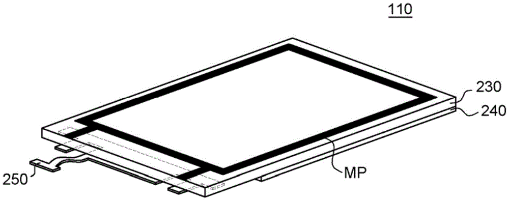
图2B是示出处于单元状态的显示面板的底表面的显示面板的透视图。其中下基板230和上基板240彼此接合为彼此间隔开的结构被称为单元(cell)。也就是说,图2B示出显示面板110的上偏振板220和下偏振板210没有接合到单元的状态。在根据本公开的示例性实施方案的显示面板110中,具有闭环形状的金属图案MP沿下基板230的底表面的边缘形成。FIG. 2B is a perspective view of the display panel showing the bottom surface of the display panel in a unit state. A structure in which the
更具体地,具有比导电层IM的薄层电阻更低的薄层电阻的金属图案MP沿导电层IM的边缘形成为闭环形状,以减小或最小化导电层IM的相对远离FPC连接焊盘251的点与导电层IM相对接近FPC连接焊盘251的点之间的电位差。具有比导电层IM的薄层电阻更低的薄层电阻的金属图案MP用作导电通道(highway)以将具有减小的或最小化的RC延迟的预定电信号从FPC连接焊盘251均匀地转移至导电层IM的整个区域。More specifically, the metal pattern MP having a lower sheet resistance than that of the conductive layer IM is formed in a closed-loop shape along the edge of the conductive layer IM to reduce or minimize the relative distance of the conductive layer IM from the FPC connection pads. The potential difference between the point of 251 and the point of the conductive layer IM relatively close to the
金属图案MP包括至少两个分支、延伸部EX。金属图案MP的延伸部EX朝向金属图案MP的环的外侧突出。换句话说,延伸部EX朝向显示面板110的边缘突出。延伸部EX被设置为与FPC连接焊盘251相邻。稍后将参照图3和图4对金属图案MP和延伸部EX的具体位置进行描述。The metal pattern MP includes at least two branches, extensions EX. The extension portion EX of the metal pattern MP protrudes toward the outside of the ring of the metal pattern MP. In other words, the extension EX protrudes toward the edge of the
图3是图2B所示的显示面板的底表面的放大平面图。FIG. 3 is an enlarged plan view of the bottom surface of the display panel shown in FIG. 2B .
在从有源区A/A到非有源区I/A上方连续沉积的导电层IM可以设置在下基板230的底表面上。导电层IM有利地具有在可见光波长范围内小于1%的光反射率。因此,其可以用作在显示装置100内部产生并且辐射到外部的光的路径。另外,导电层IM有利地具有小于300Ω/sq的薄层电阻。因此,其可以更快速和均匀地形成等电位表面。The conductive layer IM continuously deposited over from the active region A/A to the inactive region I/A may be disposed on the bottom surface of the
导电层IM可以具有其中具有高折射率的层和具有低折射率的层依次交替地层叠的多层结构。例如,导电层IM可以包括依次层叠的折射率为n1的第一无机层、折射率为n2的第二无机层和折射率为n3的第三无机层。本文中,n1、n2和n3相对于可见光波长范围内的光可以具有n2<n1和n2<n3的关系。第一无机层至第三无机层中的一个或更多个无机层可以由导电材料形成。例如,第三无机层可以通过沉积铟锡氧化物形成。在这种情况下,第三无机层可以形成为至少
同时,当第三无机层由诸如铟锡氧化物(ITO)的导电透明材料形成时,第三无机层的透光率随着第三无机层的厚度的增加而减小。为了补偿第三无机层的透光率,具有低折射率的第二无机层和具有高折射率的第一无机层交替地层叠。例如,第一无机层可以由氧化铌(Nb2O5)形成,第二无机层可以由氧化硅(SiO2)形成,第三无机层可以由铟锡氧化物(ITO)形成。因此,可以获得具有小于1%的光反射率,95%或更大的透光率和300Ω/sq或更小的薄层电阻的导电层IM。Meanwhile, when the third inorganic layer is formed of a conductive transparent material such as indium tin oxide (ITO), the light transmittance of the third inorganic layer decreases as the thickness of the third inorganic layer increases. In order to compensate the light transmittance of the third inorganic layer, second inorganic layers having a low refractive index and first inorganic layers having a high refractive index are alternately stacked. For example, the first inorganic layer may be formed of niobium oxide (Nb 2 O 5 ), the second inorganic layer may be formed of silicon oxide (SiO 2 ), and the third inorganic layer may be formed of indium tin oxide (ITO). Therefore, the conductive layer IM having a light reflectivity of less than 1%, a light transmittance of 95% or more and a sheet resistance of 300Ω/sq or less can be obtained.
另外,在形成铟锡氧化物(ITO)的第三无机层的情况下,如果为了减小导电层IM的薄层电阻而增加第三无机层的厚度,那么光反射率增加到1%或更大,或者透光率降低至小于90%。因此,调整用于形成铟锡氧化物(ITO)的第三无机层的条件,使得导电层IM有利地具有300Ω/sq或更小的薄层电阻和1%或更小的光反射率。如果导电层IM的尺寸由于显示面板110的尺寸的增加而增加,那么单独导电层IM的电阻率可能不能够在导电层IM的整个区域上快速形成等电位面。当通过施加点将电信号施加到导电层IM时,在施加点与位于远离施加点的导电层IM处的点之间可能存在电位差。这种电位差与导电层IM的尺寸成比例。In addition, in the case of forming the third inorganic layer of indium tin oxide (ITO), if the thickness of the third inorganic layer is increased in order to reduce the sheet resistance of the conductive layer IM, the light reflectivity is increased to 1% or more large, or the transmittance is reduced to less than 90%. Therefore, the conditions for forming the third inorganic layer of indium tin oxide (ITO) are adjusted so that the conductive layer IM advantageously has a sheet resistance of 300Ω/sq or less and a light reflectivity of 1% or less. If the size of the conductive layer IM increases due to an increase in the size of the
为了解决这个问题,用于形成导电层IM的等电位的预定电信号通过金属图案MP施加,金属图案MP具有比导电层IM的薄层电阻小的薄层电阻,并且有利地与导电层IM的整个边缘接触。也就是说,有利的是,金属图案MP和导电层IM形成尽可能大的界面而不侵入有源区A/A。因此,预定的电信号能够通过由金属图案MP与导电层IM之间的接触形成的界面施加到导电层IM。In order to solve this problem, a predetermined electric signal for forming the equipotential of the conductive layer IM is applied through the metal pattern MP, the metal pattern MP has a sheet resistance smaller than that of the conductive layer IM, and is advantageously similar to that of the conductive layer IM. Entire edge contact. That is, it is advantageous that the metal pattern MP and the conductive layer IM form an interface as large as possible without invading the active region A/A. Therefore, a predetermined electrical signal can be applied to the conductive layer IM through the interface formed by the contact between the metal pattern MP and the conductive layer IM.
具有比导电层IM的薄层电阻小的薄层电阻的金属图案MP设置在其上形成有导电层IM的下基板230的底表面上。因此,金属图案MP与导电层IM的底表面接触。更具体地,金属图案MP形成与导电层IM的第三无机层的界面。换句话说,金属图案MP与第三无机层的为导电层IM提供导电性的一个表面直接接触。随着不透明金属图案MP与透光导电层IM之间的界面的尺寸增加,金属图案MP与导电层IM之间的接触电阻减小。因此,当设置成对应于非有源区域I/A时,金属图案MP可以沿导电层IM的一个表面的边缘形成为闭环形状,以便增加或最大化金属图案MP与透光导电层IM之间的界面的尺寸。例如,如果显示面板110在平面图中具有正方形形状,那么金属图案MP可以具有正方形环形状。此外,金属电极可以具有闭环形状,但不限于此。例如,参照图2B至图3,在两个延伸部EX之间延伸的金属图案MP的一部分可以打开,从而金属图案MP可以具有开环形状。A metal pattern MP having a sheet resistance smaller than that of the conductive layer IM is disposed on the bottom surface of the
当金属图案MP不透明时,如上所述期望尽可能不侵入有源区A/A。换句话说,金属图案MP被设置成使得金属图案MP与透光导电层IM之间的界面的尺寸增大或最大化,并且同时金属图案MP尽可能不侵入有源区A/A。例如,金属图案MP可以围绕下基板230的有源区A/A。也就是说,金属图案MP可以沿导电层IM的底表面的边缘形成闭环形状。金属图案MP可以使用金属墨印刷在下基板230的底表面上以具有闭环形状。When the metal pattern MP is opaque, as described above, it is desirable not to invade the active area A/A as much as possible. In other words, the metal pattern MP is disposed such that the size of the interface between the metal pattern MP and the light-transmitting conductive layer IM is increased or maximized, and at the same time, the metal pattern MP does not intrude into the active area A/A as much as possible. For example, the metal pattern MP may surround the active area A/A of the
金属墨是指其中高导电性颗粒如金属颗粒分散在溶剂中的糊料状态的组合物。金属墨具有适于通过喷墨印刷法形成线状的流动性、粘度和表面张力。金属墨可以包括作为基底的在室温下为液态并且金属颗粒可以均匀分散的有机溶剂。另外,金属墨可以包含促进金属颗粒在溶剂中均匀分散的分散剂。例如,有机溶剂可以是极性有机材料,例如具有适当粘度的醇官能团的三乙二醇单乙醚(TGME,C8H18O4)。另外,有机溶剂可以是碱性材料,例如四甲基氢氧化铵(TMAH,(CH3)4NOH))。例如包含在金属墨中的有机溶剂可以是极性有机溶剂。考虑到金属颗粒的性质、分散剂的性质、进行印刷的基板的性质以及在烧结后的清洁工艺中使用的清洁溶液的性质,金属墨中可以包括具有不同性质的有机溶剂。The metallic ink refers to a composition in a paste state in which highly conductive particles such as metal particles are dispersed in a solvent. The metallic ink has fluidity, viscosity, and surface tension suitable for forming a thread by an inkjet printing method. The metallic ink may include, as a substrate, an organic solvent that is liquid at room temperature and that metal particles can be uniformly dispersed. In addition, the metallic ink may contain a dispersant that promotes uniform dispersion of the metallic particles in the solvent. For example, the organic solvent may be a polar organic material such as triethylene glycol monoethyl ether ( TGME , C8H18O4 ) with alcohol functionality of appropriate viscosity. Additionally, the organic solvent may be an alkaline material such as tetramethylammonium hydroxide (TMAH, (CH 3 ) 4 NOH)). For example, the organic solvent contained in the metallic ink may be a polar organic solvent. Organic solvents with different properties may be included in the metal ink in consideration of the properties of the metal particles, the properties of the dispersant, the properties of the substrate on which printing is performed, and the properties of the cleaning solution used in the post-sintering cleaning process.
金属图案MP可以包含具有优异导电性的金属材料或金属合金材料,例如银(Ag)、铜(Cu)、钼(Mo)、铬(Cr)等。也就是说,包含在金属墨中的金属颗粒可以是具有优异导电性的金属材料或金属合金材料,例如银(Ag)、铜(Cu)、钼(Mo)、铬(Cr)等。如果导电层IM包括铟-锡氧化物(ITO)以实现高透光率,那么金属图案MP有利地具有1Ω/mm或更小的线电阻,以使金属图案MP具有比导电层IM的薄层电阻小的薄层电阻。薄层电阻是通过将包括测量对象的厚度和形状的各种校正因子应用到测量对象的独特特性的线电阻而导出的值。通常,通过4-探针测试来测量薄层电阻。The metal pattern MP may contain a metal material or metal alloy material having excellent conductivity, such as silver (Ag), copper (Cu), molybdenum (Mo), chromium (Cr), and the like. That is, the metal particles contained in the metal ink may be a metal material or a metal alloy material having excellent conductivity, such as silver (Ag), copper (Cu), molybdenum (Mo), chromium (Cr), or the like. If the conductive layer IM includes indium-tin oxide (ITO) to achieve high light transmittance, the metal pattern MP advantageously has a line resistance of 1Ω/mm or less so that the metal pattern MP has a thinner layer than the conductive layer IM Low resistance sheet resistance. Sheet resistance is a value derived by applying various correction factors including the thickness and shape of the measurement object to the line resistance of the unique characteristic of the measurement object. Typically, sheet resistance is measured by a 4-probe test.
确保低的薄层电阻意味着确保低的线电阻。例如,如果金属图案MP由具有比铟-锡氧化物(ITO)的电阻率低的电阻率的银(Ag)形成,那么在导电层IM与金属图案MP之间的接触电阻减小。如果金属图案MP由银(Ag)形成,那么金属图案MP的线电阻可以减小到至少0.005Ω/mm。因此,金属图案MP可以具有0.005Ω/mm至1Ω/mm的线电阻。如果金属图案MP由银(Ag)形成,那么当金属图案MP具有400nm至800nm的宽度W和0.1μm至1μm的高度时,金属图案MP可以具有0.005Ω/mm至1Ω/mm的线电阻。也就是说,如果金属图案MP由银(Ag)形成,那么当金属图案MP具有400nm至800nm的宽度W和0.1μm至1μm的高度时,金属图案MP具有比包含铟锡氧化物(ITO)的导电层IM的薄层电阻更低的薄层电阻。如果金属图案MP由银(Ag)形成,那么当用于形成金属图案MP的金属墨包含重量比为20%至30%的银(Ag)颗粒并且金属墨具有10cp至30cp的粘度时,金属图案MP可以具有400nm至800nm的宽度W和0.1μm至1μm的高度。Ensuring low sheet resistance means ensuring low wire resistance. For example, if the metal pattern MP is formed of silver (Ag) having a lower resistivity than that of indium-tin oxide (ITO), the contact resistance between the conductive layer IM and the metal pattern MP decreases. If the metal pattern MP is formed of silver (Ag), the line resistance of the metal pattern MP may be reduced to at least 0.005Ω/mm. Therefore, the metal pattern MP may have a line resistance of 0.005Ω/mm to 1Ω/mm. If the metal pattern MP is formed of silver (Ag), when the metal pattern MP has a width W of 400 to 800 nm and a height of 0.1 to 1 μm, the metal pattern MP may have a line resistance of 0.005 to 1 Ω/mm. That is, if the metal pattern MP is formed of silver (Ag), when the metal pattern MP has a width W of 400 nm to 800 nm and a height of 0.1 μm to 1 μm, the metal pattern MP has more The sheet resistance of the conductive layer IM is lower sheet resistance. If the metal pattern MP is formed of silver (Ag), when the metal ink used to form the metal pattern MP contains silver (Ag) particles in a weight ratio of 20 to 30% and the metal ink has a viscosity of 10 cp to 30 cp, the metal pattern MP The MP may have a width W of 400 nm to 800 nm and a height of 0.1 μm to 1 μm.
金属图案MP可以形成为足够厚以具有比透光导电层IM的薄层电阻较低的薄层电阻。为了通过沉积形成厚的金属图案MP,通常需要长的制造时间,这意味着显示面板110在制造工艺期间可能长时间暴露于损伤。也就是说,用于制造金属图案MP的环境条件和用于制造金属图案MP的时间量是对于显示装置100的性能被管理(managed)的主要因素。The metal pattern MP may be formed thick enough to have a lower sheet resistance than that of the light-transmitting conductive layer IM. In order to form a thick metal pattern MP by deposition, a long manufacturing time is generally required, which means that the
如果通过印刷或点胶制造金属图案MP,那么与通过沉积制造金属图案MP的情况相比,可能降低金属图案MP的表面或边缘处的均匀性。然而,可以在短得多的时间内形成具有大厚度的金属图案MP。也就是说,如果金属图案MP由可以被印刷或点胶的材料形成,那么与金属图案MP由可以被沉积的材料形成的情况相比,金属图案MP的表面或边缘可以具有低均匀性。由于对于具有几个μm厚度或几百个nm宽度的厚且宽的金属图案MP,与构成微集成电路的金属图案相比,形状精度相对不重要。因此,如果形成具有几个μm的厚度或几百个nm的宽度的厚且宽的金属图案MP,那么优选通过印刷或点胶制造金属图案MP。当通过印刷或点胶制造金属图案MP时,可以通过调节金属墨的排出量或粘度来调整金属图案MP的厚度和宽度。If the metal pattern MP is manufactured by printing or dispensing, the uniformity at the surface or edge of the metal pattern MP may be reduced compared to the case where the metal pattern MP is manufactured by deposition. However, the metal pattern MP with a large thickness can be formed in a much shorter time. That is, if the metal pattern MP is formed of a material that can be printed or dispensed, the surface or edge of the metal pattern MP may have low uniformity compared to a case where the metal pattern MP is formed of a material that can be deposited. Since for a thick and wide metal pattern MP having a thickness of several μm or a width of several hundreds of nm, the shape accuracy is relatively unimportant compared to the metal pattern constituting the micro-integrated circuit. Therefore, if a thick and wide metal pattern MP having a thickness of several μm or a width of several hundreds of nm is formed, it is preferable to manufacture the metal pattern MP by printing or dispensing. When the metal pattern MP is manufactured by printing or dispensing, the thickness and width of the metal pattern MP can be adjusted by adjusting the discharge amount or viscosity of the metal ink.
如上所述,金属图案通过印刷或点胶金属墨形成。因此,金属墨由可以被印刷或点胶的材料形成。印刷或点胶方法可以是气动类型、压电类型和电类型,这仅是示例,但可以不限于此。气动型方法使用气压控制和基于微处理器的计时器。压电型方法是使用压电原理推动液体的方法。电类型方法是在线圈上形成电磁并且推动液体的方法。As mentioned above, the metallic pattern is formed by printing or dispensing metallic ink. Thus, metallic inks are formed from materials that can be printed or dispensed. The printing or dispensing method may be pneumatic type, piezoelectric type, and electric type, which are only examples, but may not be limited thereto. Pneumatic methods use air pressure control and a microprocessor-based timer. Piezo-type methods are methods of propelling liquids using the piezoelectric principle. The electric type method is a method in which an electromagnetism is formed on a coil and a liquid is pushed.
例如,气动型方法可以是通过利用其端部的球形顶端和弹簧驱动气动活塞来排出液体的方法。如果活塞由气动压力升高,那么注射器中的液体通过气动压力通过喷射喷嘴排出。如果活塞的气动压力被阻塞,那么活塞通过复位弹簧压力阻塞喷射喷嘴并且停止液体的排出。液体通过反复进行利用气压的活塞运动和利用复位弹簧压力的操作来排出。For example, a pneumatic type method may be a method of discharging liquid by driving a pneumatic piston with a spherical tip at its end and a spring. If the piston is raised by pneumatic pressure, the liquid in the syringe is expelled through the spray nozzle by pneumatic pressure. If the pneumatic pressure of the piston is blocked, the piston blocks the spray nozzle by the return spring pressure and stops the discharge of the liquid. The liquid is discharged by repeating the piston movement by air pressure and the operation by the pressure of the return spring.
例如,压电型方法可以是通过在注射器中安装利用压电致动器的压电线性电动机来排出液体并且使用压电性作为驱动源的方法,所述压电致动器可以通过施加电压精确地控制位移。由于可以进行高速和高精度的控制,所以可以以非常小的量排出液体。另外,可以根据驱动电压、驱动频率和施加到压电元件的施加电压的波形的变化来控制液体的排出量。For example, a piezoelectric type method may be a method in which liquid is discharged by installing a piezoelectric linear motor using a piezoelectric actuator, which can be precisely applied by applying a voltage, as a driving source by installing a piezoelectric linear motor in a syringe and using piezoelectricity as a driving source. control the displacement. Since high-speed and high-precision control is possible, the liquid can be discharged in a very small amount. In addition, the discharge amount of the liquid can be controlled according to changes in the driving voltage, the driving frequency, and the waveform of the applied voltage applied to the piezoelectric element.
例如,电类型(electric-type)方法可以是通过根据螺线管驱动方法上下移动线圈来排出液体的方法。在类似压电方法的电类型方法中,致动器可以安装在注射器中。电磁阀可以以低功率控制并且使用电信号,因此,可以快速控制打开/关闭时间。另外,可以通过适当地调整线圈的卷绕次数和输入电流来精确地控制液体的排出量。For example, an electric-type method may be a method of discharging liquid by moving a coil up and down according to a solenoid driving method. In an electrical type method like the piezoelectric method, the actuator can be installed in the syringe. Solenoid valves can be controlled with low power and use electrical signals, therefore, opening/closing times can be quickly controlled. In addition, the discharge amount of the liquid can be precisely controlled by appropriately adjusting the number of windings of the coil and the input current.
如上所述,根据本公开的示例性实施方案的金属图案MP可以通过印刷或点胶形成。金属图案MP通过干燥和固化印刷的金属墨而形成。在这种情况下,包含在金属墨中的溶剂或分散剂可以保留在金属图案MP中。也就是说,金属图案MP可以不仅包括金属材料或金属合金材料,而且包括诸如溶剂或分散剂的有机材料。As described above, the metal pattern MP according to the exemplary embodiment of the present disclosure may be formed by printing or dispensing. The metal pattern MP is formed by drying and curing the printed metal ink. In this case, the solvent or dispersant contained in the metal ink may remain in the metal pattern MP. That is, the metal pattern MP may include not only a metal material or a metal alloy material but also an organic material such as a solvent or a dispersant.
通过从金属墨中除去溶剂来除去金属墨的流动性,并且在高温下烧结金属颗粒,以便使得印刷在下基板230上的金属墨被固定到下基板230。因此,可以获得固化的金属图案MP。The fluidity of the metal ink is removed by removing the solvent from the metal ink, and the metal particles are sintered at a high temperature, so that the metal ink printed on the
然后,使用蒸馏水进行洗涤过程,使得下偏振板210可以接合到下基板230的底表面而没有异物。由于在金属墨被干燥和烧结时在下基板230和上基板240上产生和保留了各种异物,因此通常期望洗涤单元的表面。为了避免在使用蒸馏水的洗涤过程中金属图案MP的损失,在洗涤过程之前利用保护涂层OC覆盖金属图案MP。为了使金属图案MP与其他部件绝缘,保护涂层OC可以包括绝缘材料。例如,保护涂层OC可以包括四甲基氢氧化铵基(TMAH,(CH3)4NOH))、乙二醇基或聚酰亚胺基材料。类似于金属图案MP,保护涂层OC可以通过在下基板230上印刷具有粘性和流动性的保护材料来形成,以覆盖金属图案MP,然后固化保护材料。保护涂层OC还可以沿非有源区I/A围绕有源区A/A,以便不侵入有源区A/A。Then, a washing process is performed using distilled water so that the lower
由于保护涂层OC覆盖金属图案MP,所以保护涂层OC可以具有比金属图案MP的宽度大的宽度。因此,存在下基板230与保护涂层OC接触而其间没有金属图案MP的区域。金属图案MP的延伸部EX延伸到显示面板的边缘。另外,在金属图案MP的延伸部EX的端部分别形成有敞开焊盘OP,并且保护涂层OC使敞开焊盘OP露出。也就是说,除了敞开焊盘OP之外,金属图案MP被绝缘保护涂层OC覆盖,使得限定敞开焊盘OP。Since the protective coating OC covers the metal pattern MP, the protective coating OC may have a width greater than that of the metal pattern MP. Therefore, there is a region where the
下偏振板210接合到其上形成有金属图案MP和保护涂层OC的下基板230的底表面。稍后将参照图4和图5对下偏振板210与金属图案MP之间的位置关系和敞开焊盘OP的位置的细节进行描述。The lower
图4是示出位于显示面板的下基板230的底表面上的金属图案MP的延伸部EX与位于下基板230的顶表面上的FPC 250的连接结构的显示面板110的部分透视图。图5是放大在图4中示出的区域Z的放大的透视图。4 is a partial perspective view of the
在用蒸馏水冲洗处理之后,下偏振板210和上偏振板220分别接合至其中上基板240和下基板230接合的单元的底表面和顶表面。下偏振板210接合至下基板230的底表面以与金属图案MP交叠。在这种情况下,下偏振板210露出金属图案MP的延伸部EX以使敞开焊盘OP不被下偏振板210覆盖。另外,下偏振板210可以接合为与有源区A/A交叠而不与延伸部EX交叠。如上所述,FPC连接焊盘251设置在FPC250的突出的而不与下基板230交叠的部分区域上。敞开焊盘OP设置在从金属图案MP突出的延伸部EX上。FPC250的突出的而不与下基板230交叠的一部分区域和延伸部EX与其间的下基板230交叠,使得FPC连接焊盘251与敞开焊盘OP相邻。另外,电连接FPC连接焊盘251和敞开焊盘OP的连接构件410形成在FPC连接焊盘251、下基板230的侧面以及敞开焊盘OP上。可以通过以点形状印刷金属墨然后使金属墨固化来形成连接构件410。金属墨可以是银(Ag)糊料。因此,连接构件410可以是热固化的银(Ag)糊料。也就是说,敞开焊盘OP被热固化的银(Ag)糊料覆盖。After rinsing treatment with distilled water, the lower
参照图5,将详细描述在FPC连接焊盘251与敞开焊盘OP之间的连接。FPC连接焊盘251和敞开焊盘OP朝着相同的方向露出。也就是说,FPC连接焊盘251和敞开焊盘OP朝着显示面板110的底表面露出。另外,沿着下基板230的侧面印刷金属墨以将FPC连接焊盘251连接至敞开焊盘OP。在这种情况下,可以通过连续放电方法或与重复脉冲对应的放电方法来印刷金属墨。金属墨可以覆盖敞开焊盘OP和FPC连接焊盘251的全部,或者可以仅覆盖敞开焊盘OP的或FPC连接焊盘251的一部分。因而,连接构件410可以设置为覆盖敞开焊盘OP的一部分和FPC连接焊盘251的一部分。例如,金属墨可以包括银(Ag)。因此,连接构件410可以是由银(Ag)形成的流线型结构。5, the connection between the
图6是沿着图4的线A-A’截取的截面图。更具体地,图6是示意性示出沿着图4的线A-A’所截取的显示面板110的截面的截面图。Fig. 6 is a cross-sectional view taken along line A-A' of Fig. 4 . More specifically, FIG. 6 is a cross-sectional view schematically showing a cross-section of the
参照图6,根据本公开的示例性实施方案的显示面板110被分成有源区A/A和在有源区A/A的外围上的非有源区I/A。有源区A/A指的是在显示面板110上实际显示图像的区域,并且非有源区I/A指的是在显示面板110上的除了实际显示图像的区域之外的区域。非有源区I/A位于有源区A/A周围以围绕有源区A/A。例如,非有源区I/A可以具有诸如环形的闭环形状。6 , the
彼此面对的上基板240和下基板230也被分成有源区A/A和围绕有源区A/A的非有源区I/A。下基板230可以具有比上基板240的尺寸更大的尺寸。下基板230和上基板240可以起支承构件和保护构件的作用,以及包括在显示面板110中的各种部件设置在保护构件上。下基板230和上基板240可以以平坦的状态固定或者以弯曲的状态固定,或者可以重复地弯曲和伸展。下基板230和上基板240可以由玻璃或基于塑料的聚合物材料形成。下基板230和上基板240具有透光特性因而可以是透明或半透明的。The
显示面板110包括在彼此面对接合的下基板230与上基板240之间的滤色器层232、光控制层270以及像素阵列层242。下基板230和上基板240接合为如彼此隔开一样的状态被称为单元(cell),像素阵列层242设置在下基板230上,滤色器层232设置在上基板240上。在单元状态下的显示面板110包括在上基板240与下基板230之间的光控制层270。光控制层270包括光控制材料。上偏振板220和下偏振板210可以以单元状态分别接合至显示面板110的顶表面和底表面。The
光控制材料控制和过滤由显示装置100生成的光以使显示装置100的每个像素发射具有特定亮度的光。例如,光控制材料可以是使得各个像素能够利用从在光控制材料的背部的背光单元120生成的光的极性而发射具有受控的亮度的光的液晶材料。可替选地,光控制材料可以是其中各个像素发射具有受控的亮度的光的有机发光元件。也就是说,在上基板240与下基板230之间的预定间隙中,可以设置液晶或者有机发光元件。图1示出了其中根据本公开的示例性实施方案的显示装置100是包括背光单元120的液晶显示装置的示例。然而,本公开不限于此。应该理解的是,在有机发光显示装置中,不包括用作光控制材料的有机发光元件和背光单元120,而单独包括压敏触摸传感器125。The light control material controls and filters the light generated by the
为了使上基板240与下基板230接合,在上基板240与下基板230之间的非有源区I/A上涂覆有密封剂260。光控制层270被密封剂260围绕。In order to bond the
设置在上基板240的底表面上的滤色器层232被分成多个滤色器并且可以包括黑矩阵233以覆盖显示面板110的非有源区I/A。黑矩阵233可以包括光敏颜料或炭黑。黑矩阵233可以吸收光并且不可以反射光。黑矩阵233被配置成覆盖在黑矩阵233下方的各种不同部件以在当用户观看显示装置100时可以不被用户视觉地识别。金属图案MP设置在黑矩阵233下方并且还可以被黑矩阵233覆盖。The
设置在下基板230的顶表面上的像素阵列层242包括分别对应于多个像素的多个像素驱动电路。内嵌式电容触摸传感器243嵌入在像素阵列层242中。The
根据本公开的示例性实施方案的显示装置100包括直接设置在显示面板110内的下基板230上的内嵌式电容触摸传感器243。另外,根据本公开的示例性实施方案的显示装置100包括在显示面板110外部的压敏触摸传感器125。也就是说,根据本公开的示例性实施方案的显示装置100通过结合多个触摸传感器来识别触摸。因而,显示装置100包括在显示面板110的上基板240与下基板230之间的内嵌式电容触摸传感器243以及在显示面板110下方的压敏触摸传感器125。图6示出了其中显示面板110包括设置在上基板240和下基板230之间的内嵌式电容触摸传感器243的实例。然而,本公开不限于此。显示面板110可以包括各种不同类型的传感器之一,例如设置在上基板240的顶表面上的盒上式触摸传感器或者设置在上基板240的顶表面和下基板230的顶表面上的混合触摸传感器。压敏触摸传感器125可以设置在显示面板110下方,如嵌入在背光单元120中一样。The
在这种情况下,内嵌式电容触摸传感器243可以是投射式(projected)电容触摸传感器。投射式电容触摸传感器基于当用户的手指触摸显示装置100时在触摸传感器与具有静电的手指之间积累并且通过用户的身体流动的电荷与当不进行接触时所积累的电荷之间的电荷量的变化来识别触摸和触摸坐标。此处,压敏触摸传感器125可以是电阻式触摸传感器。根据本公开的示例性实施方案的显示装置100将利用内嵌式电容触摸传感器243获得触摸坐标并且还利用压敏触摸传感器125获得触摸压力。可以同时识别触摸坐标和触摸压力。为此,压敏触摸传感器125可以施加有第一触摸驱动信号并且内嵌式电容触摸传感器243可以施加有第二触摸驱动信号。In this case, the in-cell
显示面板110的驱动时间段可以是显示图像的时间段与识别用户触摸的时间段的重复(repetition)。待被共同地施加至所有的像素的电压(例如,公共电压)通过公共电极施加至各个像素,公共电极是构成各个像素的两个电极之一。此处,如果公共电极包括多个公共电极组(block),则在通过显示面板110显示图像的驱动时间段期间施加公共电压。此外,可以在通过显示面板110识别用户的触摸的驱动时间段期间施加触摸感测信号。也就是说,内嵌式电容触摸传感器243可以包括多个公共电极组。The driving period of the
如果公共电极仅用于在显示面板110上显示图像,则公共电极可以被制造成相对于所有的像素集成的薄膜型电极。然而,如果公共电极用于在显示面板110上显示图像并且还在显示面板上识别用户的触摸坐标,则公共电极有利地被分成多个公共电极组以识别用户的触摸坐标。因此,内嵌式电容触摸传感器243可以包括多个公共电极组并且可以被实现为适合于时分(time division)驱动以起到公共电极和触摸电极的作用。If the common electrode is only used for displaying an image on the
更具体地,如果显示面板110被驱动为在显示驱动模式期间显示图像,则公共电压被施加至所述多个公共电极组。也就是说,所述多个公共电极组起到面对像素电极并且形成电场的公共电极的作用。另外,如果显示面板110被驱动为在触摸驱动模式期间识别用户触摸,则触摸驱动电压被施加至所述多个公共电极组。然后,通过识别在触摸指示物(例如,用户的手指、笔等)与对应于触摸指示物的位置的公共电极组之间形成的电容来感测用户的触摸。也就是说,所述多个公共电极还起到内嵌式电容触摸传感器243的作用。More specifically, if the
为了向所述多个公共电极组传递公共电压或者第二触摸驱动信号,可以连接分别对应于多个公共电极组的多个触摸信号线。如果显示面板110的驱动模式是显示驱动模式,从公共电压供应单元供应的公共电压通过多个触摸信号线被等同地施加至多个公共电极组中的所有组。如果显示面板110的驱动模式是触摸驱动模式,则在第二触摸集成电路中生成的第二触摸驱动信号通过多个触摸信号线被传递至多个公共电极组中的所有公共电极组或一些电极组。In order to transmit a common voltage or a second touch driving signal to the plurality of common electrode groups, a plurality of touch signal lines respectively corresponding to the plurality of common electrode groups may be connected. If the driving mode of the
由第二触摸集成电路提供的第二触摸驱动信号或者由公共电压供给单元提供的公共电压通过多个触摸信号线被转移至多个公共电极组。第二触摸集成电路或公共电压供给单元被设置在显示面板110的边缘的一个侧上。因而,多个触摸信号线被连接至各个公共电极组并且延伸至显示面板110的边缘的一个侧。从多个公共电极组中的每一个连接至显示面板110的边缘的一个侧的多个触摸信号线被布置为与在像素阵列层242上的有源区A/A对应。多个公共电极组可以以与多个触摸信号线接触的方式彼此连接或可以通过另外的接触图案连接至彼此。也就是说,多个公共电极组中的每一个组被电连接至多个触摸信号线。The second touch driving signal provided by the second touch integrated circuit or the common voltage provided by the common voltage supply unit is transferred to the plurality of common electrode groups through the plurality of touch signal lines. The second touch integrated circuit or the common voltage supply unit is disposed on one side of the edge of the
此处,多个触摸信号线设置在有源区A/A中的多个公共电极组与下基板230之间。换言之,多个触摸信号线设置在有源区A/A中的像素阵列层242上。也就是说,多个触摸信号线像像素驱动电路的一个部件一样被包含在像素驱动电路中。然而,多个触摸信号线的位置不限于此。例如,多个触摸信号线可以设置为与构成多个薄膜晶体管的部件在相同的平面上或者可以被设置为比所述部件高。作为示例,多个公共电极组设置在包含在像素驱动电路中的多个薄膜晶体管上。Here, a plurality of touch signal lines are disposed between a plurality of common electrode groups in the active area A/A and the
FPC 250可以包括各种集成电路,例如第一触摸集成电路或第二触摸集成电路。芯片型第一触摸集成电路或第二触摸集成电路可以接合至FPC 250。在FPC 250中,可以设置有设置在显示面板外部的连接至第一触摸集成电路或第二触摸集成电路的线。此处,第二触摸集成电路和第一触摸集成电路可以是不同的部件或者可以是相同的部件。否则,在FPC250中,可以设置其中来自系统的接地电压施加至其上的线。FPC 250的延伸线形成FPC连接焊盘251的端部。预定的电信号从FPC连接焊盘251施加至导电层IM。此处,金属图案MP的敞开焊盘OP通过连接构件410电连接至FPC连接焊盘251。因而,导电层IM可以电连接至FPC连接焊盘251。The
沉积导电层IM以覆盖下基板230的底表面。也就是说,导电层IM覆盖下基板230的通常与有源区A/A和非有源区I/A对应的整个底表面。此外,可以沉积导电层IM以覆盖下基板230的底表面并且不与非有源区I/A的部分交叠。导电层IM设置在压敏触摸传感器125与内嵌式电容触摸传感器243之间。可以在下基板230的底表面上沉积导电层IM以设置在压敏触摸传感器125与内嵌式电容触摸传感器243之间。导电层IM提供在下基板230的底表面上的等势面因而可以降低或最小化各种不同的电信号之间的干扰。A conductive layer IM is deposited to cover the bottom surface of the
例如,导电层IM可以抑制在第一触摸驱动信号与第二触摸驱动信号之间的干扰。为此,导电层IM可以电连接至系统的接地线以接地。也就是说,导电层IM可以向显示面板110提供平顺的放电路径。在这种情况下,施加至导电层IM的预定的电信号是接地电压。可替选地,为了感测用户的触摸压力,导电层IM可以是面对压敏触摸传感器125的触摸传感器。在这种情况下,施加至导电层IM的预定的电信号可以是第三触摸驱动信号,第三触摸驱动信号响应于第一触摸驱动信号而形成电势差因而能感测压力。可替选地,为了感测用户的触摸压力,导电层IM可以是压敏触摸传感器125的次级触摸传感器。在这种情况下,与压敏触摸传感器125类似,导电层IM可以通过第一触摸集成电路而施加有第一触摸驱动信号。For example, the conductive layer IM may suppress interference between the first touch driving signal and the second touch driving signal. To this end, the conductive layer IM may be electrically connected to the ground line of the system for grounding. That is, the conductive layer IM may provide a smooth discharge path to the
导电层IM由能够更加迅速且均匀地形成等势面的材料形成。导电层IM位于在显示装置100中生成的并且向显示装置100的外部辐射的光的路径上。因而,优选地,导电层IM可以具有优异的光学性能。例如,导电层IM可以由透光材料形成,使得从在显示面板110下方的背光单元120通过下偏振板210向显示装置100的外部辐射的光能够通过。优选地,导电层IM可以具有在可见光波段范围内为90%或更大的透光率。另外,优选地,导电层IM可以具有在可见光波长范围内小于1%的平均光反射率。因而,可以减小或最小化在通过从外部入射到显示装置100中的外部光的反射而引起的显示装置的可视性的降低。例如,导电层IM可以由铟锡氧化物(ITO)形成以具有透光特性并且还具有高的电导率。The conductive layer IM is formed of a material capable of forming an equipotential surface more rapidly and uniformly. The conductive layer IM is located on the path of light generated in the
然而,导电层IM有利地是光学透明的。因而,在导电层IM的厚度的增加方面存在限制以减小导电层IM的薄层电阻。也就是说,如果导电层IM的厚度增加以使导电层IM在短时间内成为等势面,则降低了导电层IM的透光率。因此,沿着导电层IM的边缘形成金属图案MP以使导电层IM在短时间内成为在整个区域中的均匀的等势面并且不降低导电层IM的透光率。However, the conductive layer IM is advantageously optically transparent. Thus, there is a limit in increasing the thickness of the conductive layer IM to reduce the sheet resistance of the conductive layer IM. That is, if the thickness of the conductive layer IM is increased so that the conductive layer IM becomes an equipotential surface in a short time, the light transmittance of the conductive layer IM is lowered. Therefore, the metal pattern MP is formed along the edge of the conductive layer IM to make the conductive layer IM a uniform equipotential surface in the entire area in a short time and not reduce the light transmittance of the conductive layer IM.
导电层IM通过金属图案MP和连接构件410电连接至FPC250。例如,导电层IM由铟锡氧化物(ITO)形成并且金属图案MP由银(Ag)形成,与导电层IM相比金属图案MP具有更低的薄层电阻。此处,如图6所示,在当金属图案MP位于导电层IM的底表面上时形成的界面处的接触电阻小于假设FPC250与导电层IM接触时形成的界面处的接触电阻。用具有高电导率并且电连接导电层IM与FPC 250的金属图案MP,电信号可以迅速传递至导电层IM的所有边缘。因而,导电层IM可以更加迅速且均匀地成为等势面。另外,如果连接构件410与金属图案MP由相同的材料形成,则能够降低形成在金属图案MP与连接构件410之间的界面处的接触电阻。另外,用类似金属图案MP的具有高电导率的连接构件410,电信号可以更加迅速地传递至金属图案MP的敞开焊盘OP。The conductive layer IM is electrically connected to the
图7是沿着图4的线B-B’截取的截面图。更具体地,图7是示意性示出沿着图4的线B-B’截取的显示面板110的截面的截面图。也就是说,与图6相比,图7示出了除了在图4中所示出的在显示面板110中电连接至彼此的金属图案MP的敞开焊盘OP与FPC连接焊盘251的部分之外的一部分的截面图。更具体地,图7是其中如果金属图案MP具有如在图3中所示出的两个延伸部EX则源极驱动器290设置在两个延伸部EX之间的一部分的截面图。Fig. 7 is a cross-sectional view taken along line B-B' of Fig. 4 . More specifically, FIG. 7 is a cross-sectional view schematically showing a cross-section of the
参照图7,配置为向下基板230的顶表面上的数据线施加电信号的源极驱动器290以与非有源区I/A对应的驱动集成电路(IC)的形式安装。配置为接收施加至像素阵列层242的各种电信号的焊盘244可以被设置在像素阵列层242的边缘上。焊盘244可以通过各向异性导电膜(ACF)280电连接至FPC连接焊盘251。在这种情况下,电连接至焊盘244的FPC连接焊盘251可以与如在图6中所示出的电连接至金属图案MP的FPC连接焊盘251相同或者不同。ACF膜280通过将导电颗粒分散在树脂膜内而形成。当膜由于被按压并且通过热和压力而固化时,导电颗粒通过将焊盘244与FPC连接焊盘251电连接而导电。同时,在其中延伸部EX部不突出的区域中,金属图案MP被保护涂层OC整体覆盖并且与下偏振板210交叠。金属图案MP设置为与非有源区I/A对应。7, the
也就是说,参照图4、图6和图7,在根据本公开的示例性实施方案的显示装置100中,具有闭环形状并且在非有源区I/A周围环绕的金属图案MP设置在下基板230下方。金属图案MP的各个延伸部EX设置在源极驱动器290的两侧上,并且敞开焊盘OP在每个延伸部EX的一端处露出。FPC连接焊盘251与下基板230的边缘相比进一步突出以与延伸部EX对应。FPC连接焊盘251和金属图案MP的敞开焊盘OP通过连接构件410电连接。连接构件410被固定为与下基板230的侧面接触。也就是说,覆盖下基板230的底表面的导电层IM与设置在下基板230的顶表面上的FPC250通过金属图案MP和连接构件410电连接。That is, referring to FIGS. 4 , 6 and 7 , in the
已经描述了根据本公开的示例性实施方案的显示装置100,包括光源124的背光单元120以示例的方式包括在该显示装置100中,但是本公开不限于此。例如,如果光控制材料通过通常在显示面板110外部不需要单独的光源124的有机发光元件实现,则背光单元120能够被压敏触摸传感器125取代。The
尽管已经参照附图详细地描述了本公开的示例性实施方案,但是本公开不限于此并且可以在不脱离本公开的技术概念的情况下以许多不同的形式实施。因此,提供本公开的示例性实施方案仅用于说明的目的而不限制本公开的技术概念。本公开的技术概念的范围不限于此。因此,应该理解的是,上述示例性实施方案在所有的方面是说明性的并且不限制本公开。本公开的保护范围应该基于下面的权利要求理解,并且在其等同范围内的所有技术概念应该被理解为落入本公开的范围内。Although the exemplary embodiments of the present disclosure have been described in detail with reference to the accompanying drawings, the present disclosure is not limited thereto and may be embodied in many different forms without departing from the technical concept of the present disclosure. Therefore, the exemplary embodiments of the present disclosure are provided for the purpose of illustration only and do not limit the technical concept of the present disclosure. The scope of the technical concept of the present disclosure is not limited thereto. Therefore, it should be understood that the above-described exemplary embodiments are illustrative in all respects and do not limit the present disclosure. The protection scope of the present disclosure should be understood based on the following claims, and all technical concepts within the equivalent scope thereof should be understood as falling within the scope of the present disclosure.
Claims (15)
Applications Claiming Priority (4)
| Application Number | Priority Date | Filing Date | Title |
|---|---|---|---|
| KR10-2015-0152833 | 2015-10-31 | ||
| KR20150152833 | 2015-10-31 | ||
| KR1020150190310A KR20170051111A (en) | 2015-10-31 | 2015-12-30 | A display device |
| KR10-2015-0190310 | 2015-12-30 |
Publications (2)
| Publication Number | Publication Date |
|---|---|
| CN106896552A CN106896552A (en) | 2017-06-27 |
| CN106896552B true CN106896552B (en) | 2020-12-01 |
Family
ID=58742055
Family Applications (1)
| Application Number | Title | Priority Date | Filing Date |
|---|---|---|---|
| CN201611006094.9A Active CN106896552B (en) | 2015-10-31 | 2016-10-27 | display device |
Country Status (2)
| Country | Link |
|---|---|
| KR (1) | KR20170051111A (en) |
| CN (1) | CN106896552B (en) |
Families Citing this family (4)
| Publication number | Priority date | Publication date | Assignee | Title |
|---|---|---|---|---|
| CN107797323B (en) * | 2017-11-17 | 2020-06-05 | 厦门天马微电子有限公司 | Display panel and display device |
| CN110543260B (en) | 2019-09-20 | 2024-07-26 | 深圳市道通科技股份有限公司 | Touch screen, display panel and automobile diagnosis equipment |
| CN110794923B (en) | 2019-10-21 | 2021-04-13 | 维沃移动通信有限公司 | Display module, control method and device thereof and electronic equipment |
| CN113552746B (en) * | 2021-07-23 | 2023-01-24 | 京东方(河北)移动显示技术有限公司 | Display panel and display device |
Citations (4)
| Publication number | Priority date | Publication date | Assignee | Title |
|---|---|---|---|---|
| EP0831357A2 (en) * | 1996-09-18 | 1998-03-25 | Sony Corporation | Liquid crystal display device |
| CN1497650A (en) * | 2002-09-26 | 2004-05-19 | 佳能株式会社 | Image display device and information display device |
| CN103852945A (en) * | 2012-12-03 | 2014-06-11 | 株式会社日本显示器 | Display device |
| US9293606B2 (en) * | 2011-11-15 | 2016-03-22 | Taiwan Semiconductor Manufacturing Co., Ltd. | Semiconductor device with seal ring with embedded decoupling capacitor |
Family Cites Families (7)
| Publication number | Priority date | Publication date | Assignee | Title |
|---|---|---|---|---|
| JP5033740B2 (en) * | 2007-10-26 | 2012-09-26 | 帝人株式会社 | Transparent conductive laminate and touch panel |
| CN101581800A (en) * | 2008-05-15 | 2009-11-18 | 甘国工 | Compound conducting film and touch screen using same |
| JP5458443B2 (en) * | 2010-09-14 | 2014-04-02 | 株式会社ジャパンディスプレイ | Display device with touch detection function and electronic device |
| JP2013054411A (en) * | 2011-08-31 | 2013-03-21 | Sony Corp | Information processor, information processing method, and program |
| CN104641331B (en) * | 2012-09-20 | 2017-03-08 | 株式会社村田制作所 | Touch panel |
| US9423897B2 (en) * | 2013-04-01 | 2016-08-23 | Apple Inc. | Electronic device display with shielding layer |
| US10359871B2 (en) * | 2014-09-26 | 2019-07-23 | Lg Display Co., Ltd. | Display panel and method of manufacturing the same |
-
2015
- 2015-12-30 KR KR1020150190310A patent/KR20170051111A/en not_active Withdrawn
-
2016
- 2016-10-27 CN CN201611006094.9A patent/CN106896552B/en active Active
Patent Citations (4)
| Publication number | Priority date | Publication date | Assignee | Title |
|---|---|---|---|---|
| EP0831357A2 (en) * | 1996-09-18 | 1998-03-25 | Sony Corporation | Liquid crystal display device |
| CN1497650A (en) * | 2002-09-26 | 2004-05-19 | 佳能株式会社 | Image display device and information display device |
| US9293606B2 (en) * | 2011-11-15 | 2016-03-22 | Taiwan Semiconductor Manufacturing Co., Ltd. | Semiconductor device with seal ring with embedded decoupling capacitor |
| CN103852945A (en) * | 2012-12-03 | 2014-06-11 | 株式会社日本显示器 | Display device |
Also Published As
| Publication number | Publication date |
|---|---|
| CN106896552A (en) | 2017-06-27 |
| KR20170051111A (en) | 2017-05-11 |
Similar Documents
| Publication | Publication Date | Title |
|---|---|---|
| US10402019B2 (en) | Display device | |
| TWI637297B (en) | Wiring body, wiring board, and touch detector | |
| CN203012297U (en) | Display device with touch panel | |
| CN105630226B (en) | Touch window | |
| US20110316810A1 (en) | Display device with touch panel | |
| US20100171718A1 (en) | Method for manufacturing touch panel, touch panel, display device, and electronic apparatus | |
| JP2010181747A (en) | Liquid crystal display device with touch sensor function | |
| KR102262470B1 (en) | Touch screen panel manufacturing method | |
| CN106896552B (en) | display device | |
| CN110794987A (en) | Organic Light Emitting Display Device | |
| US20190206898A1 (en) | Display device | |
| KR101901253B1 (en) | Display Device integrating with Touch Screen and Method for Manufacturing the Same | |
| CN102436323A (en) | Display device associated with touch panel and producing method thereof | |
| US20120098791A1 (en) | Touch panels, method for fabricating touch panels, display devices, and method for fabricating display devices | |
| JP5473460B2 (en) | Input device and display device including the input device | |
| JP2011039759A (en) | Touch panel device, method for manufacturing the same, display, and electronic equipment | |
| JP2011039758A (en) | Touch panel device, display, and electronic equipment | |
| KR101956086B1 (en) | Touch panel, display and method of the same | |
| JP2013045261A (en) | Touch panel sensor with color filter, liquid-crystal display, and coordinate detector | |
| KR20170050536A (en) | A display device and manufacturing method thereof | |
| KR101152716B1 (en) | Capacitive touch sensor and capacitive touch panel of integrated window panel type including the same | |
| KR102029710B1 (en) | Touch panel | |
| JP6267521B2 (en) | Liquid crystal display | |
| KR20180113081A (en) | Touch panel | |
| KR102302824B1 (en) | Touch window and touch device |
Legal Events
| Date | Code | Title | Description |
|---|---|---|---|
| PB01 | Publication | ||
| PB01 | Publication | ||
| SE01 | Entry into force of request for substantive examination | ||
| GR01 | Patent grant | ||
| GR01 | Patent grant |