CN106716441B - Event-based computer vision computing - Google Patents
Event-based computer vision computing Download PDFInfo
- Publication number
- CN106716441B CN106716441B CN201580050415.2A CN201580050415A CN106716441B CN 106716441 B CN106716441 B CN 106716441B CN 201580050415 A CN201580050415 A CN 201580050415A CN 106716441 B CN106716441 B CN 106716441B
- Authority
- CN
- China
- Prior art keywords
- sensor element
- feature
- sensor
- subject
- event
- Prior art date
- Legal status (The legal status is an assumption and is not a legal conclusion. Google has not performed a legal analysis and makes no representation as to the accuracy of the status listed.)
- Active
Links
- 238000000034 method Methods 0.000 claims abstract description 62
- 238000004364 calculation method Methods 0.000 claims abstract description 11
- 239000003550 marker Substances 0.000 claims description 11
- 230000000007 visual effect Effects 0.000 claims description 7
- 238000001514 detection method Methods 0.000 abstract description 44
- 230000008859 change Effects 0.000 abstract description 27
- 230000008569 process Effects 0.000 description 22
- 230000002093 peripheral effect Effects 0.000 description 16
- 238000004891 communication Methods 0.000 description 11
- 238000010586 diagram Methods 0.000 description 11
- 230000015654 memory Effects 0.000 description 11
- 235000019580 granularity Nutrition 0.000 description 8
- 230000003936 working memory Effects 0.000 description 8
- 230000003287 optical effect Effects 0.000 description 5
- 230000005540 biological transmission Effects 0.000 description 4
- 239000003990 capacitor Substances 0.000 description 4
- 238000012986 modification Methods 0.000 description 4
- 230000004048 modification Effects 0.000 description 4
- ORQBXQOJMQIAOY-UHFFFAOYSA-N nobelium Chemical compound [No] ORQBXQOJMQIAOY-UHFFFAOYSA-N 0.000 description 3
- 102100029469 WD repeat and HMG-box DNA-binding protein 1 Human genes 0.000 description 2
- 101710097421 WD repeat and HMG-box DNA-binding protein 1 Proteins 0.000 description 2
- 238000010276 construction Methods 0.000 description 2
- 230000007613 environmental effect Effects 0.000 description 2
- 230000006870 function Effects 0.000 description 2
- 238000009434 installation Methods 0.000 description 2
- 230000004044 response Effects 0.000 description 2
- RYGMFSIKBFXOCR-UHFFFAOYSA-N Copper Chemical compound [Cu] RYGMFSIKBFXOCR-UHFFFAOYSA-N 0.000 description 1
- 230000001133 acceleration Effects 0.000 description 1
- 238000003491 array Methods 0.000 description 1
- 230000010267 cellular communication Effects 0.000 description 1
- 230000006835 compression Effects 0.000 description 1
- 238000007906 compression Methods 0.000 description 1
- 238000004590 computer program Methods 0.000 description 1
- 238000013500 data storage Methods 0.000 description 1
- 230000006837 decompression Effects 0.000 description 1
- 238000005516 engineering process Methods 0.000 description 1
- 239000000835 fiber Substances 0.000 description 1
- 230000017525 heat dissipation Effects 0.000 description 1
- 238000007726 management method Methods 0.000 description 1
- 230000008520 organization Effects 0.000 description 1
- 239000007787 solid Substances 0.000 description 1
- 230000003068 static effect Effects 0.000 description 1
- 239000000126 substance Substances 0.000 description 1
- 230000001960 triggered effect Effects 0.000 description 1
- 230000002618 waking effect Effects 0.000 description 1
Images


Classifications
-
- G—PHYSICS
- G06—COMPUTING; CALCULATING OR COUNTING
- G06F—ELECTRIC DIGITAL DATA PROCESSING
- G06F3/00—Input arrangements for transferring data to be processed into a form capable of being handled by the computer; Output arrangements for transferring data from processing unit to output unit, e.g. interface arrangements
- G06F3/01—Input arrangements or combined input and output arrangements for interaction between user and computer
- G06F3/03—Arrangements for converting the position or the displacement of a member into a coded form
- G06F3/041—Digitisers, e.g. for touch screens or touch pads, characterised by the transducing means
- G06F3/042—Digitisers, e.g. for touch screens or touch pads, characterised by the transducing means by opto-electronic means
- G06F3/0425—Digitisers, e.g. for touch screens or touch pads, characterised by the transducing means by opto-electronic means using a single imaging device like a video camera for tracking the absolute position of a single or a plurality of objects with respect to an imaged reference surface, e.g. video camera imaging a display or a projection screen, a table or a wall surface, on which a computer generated image is displayed or projected
-
- G—PHYSICS
- G06—COMPUTING; CALCULATING OR COUNTING
- G06V—IMAGE OR VIDEO RECOGNITION OR UNDERSTANDING
- G06V10/00—Arrangements for image or video recognition or understanding
- G06V10/40—Extraction of image or video features
- G06V10/44—Local feature extraction by analysis of parts of the pattern, e.g. by detecting edges, contours, loops, corners, strokes or intersections; Connectivity analysis, e.g. of connected components
-
- G—PHYSICS
- G06—COMPUTING; CALCULATING OR COUNTING
- G06V—IMAGE OR VIDEO RECOGNITION OR UNDERSTANDING
- G06V10/00—Arrangements for image or video recognition or understanding
- G06V10/94—Hardware or software architectures specially adapted for image or video understanding
- G06V10/955—Hardware or software architectures specially adapted for image or video understanding using specific electronic processors
-
- H—ELECTRICITY
- H01—ELECTRIC ELEMENTS
- H01L—SEMICONDUCTOR DEVICES NOT COVERED BY CLASS H10
- H01L27/00—Devices consisting of a plurality of semiconductor or other solid-state components formed in or on a common substrate
- H01L27/14—Devices consisting of a plurality of semiconductor or other solid-state components formed in or on a common substrate including semiconductor components sensitive to infrared radiation, light, electromagnetic radiation of shorter wavelength or corpuscular radiation and specially adapted either for the conversion of the energy of such radiation into electrical energy or for the control of electrical energy by such radiation
- H01L27/144—Devices controlled by radiation
- H01L27/146—Imager structures
- H01L27/14643—Photodiode arrays; MOS imagers
-
- H—ELECTRICITY
- H04—ELECTRIC COMMUNICATION TECHNIQUE
- H04N—PICTORIAL COMMUNICATION, e.g. TELEVISION
- H04N25/00—Circuitry of solid-state image sensors [SSIS]; Control thereof
- H04N25/70—SSIS architectures; Circuits associated therewith
- H04N25/71—Charge-coupled device [CCD] sensors; Charge-transfer registers specially adapted for CCD sensors
- H04N25/75—Circuitry for providing, modifying or processing image signals from the pixel array
-
- H—ELECTRICITY
- H04—ELECTRIC COMMUNICATION TECHNIQUE
- H04N—PICTORIAL COMMUNICATION, e.g. TELEVISION
- H04N25/00—Circuitry of solid-state image sensors [SSIS]; Control thereof
- H04N25/70—SSIS architectures; Circuits associated therewith
- H04N25/76—Addressed sensors, e.g. MOS or CMOS sensors
- H04N25/77—Pixel circuitry, e.g. memories, A/D converters, pixel amplifiers, shared circuits or shared components
-
- G—PHYSICS
- G06—COMPUTING; CALCULATING OR COUNTING
- G06V—IMAGE OR VIDEO RECOGNITION OR UNDERSTANDING
- G06V10/00—Arrangements for image or video recognition or understanding
- G06V10/40—Extraction of image or video features
- G06V10/46—Descriptors for shape, contour or point-related descriptors, e.g. scale invariant feature transform [SIFT] or bags of words [BoW]; Salient regional features
- G06V10/467—Encoded features or binary features, e.g. local binary patterns [LBP]
Abstract
The present invention provides techniques for triggering events based on detecting changes in CV features such as edges, corners, etc., by generating calculated results based on sensor readings. The present invention also provides other techniques for detecting a CV characteristic when an event is detected based on a change in sensor readings of the sensor elements. In certain aspects, the event detection logic and the feature calculation CV vision operations may be performed individually or in combination in circuitry on the sensor or in software/firmware on the computing device.
Description
Technical Field
The present invention relates generally to enabling computer vision, and more particularly to using computer vision to improve the efficiency of detecting features.
Background
Computer vision is a field that encompasses methods of acquiring, processing, analyzing, and understanding images for use in various applications. Traditionally, a processor coupled to the sensor acquires image data from the sensor and performs certain Computer Vision (CV) operations on the information received from the sensor for detecting CV features and thus objects associated with those features. The features may include edges, corners, etc. These CV features can be used to determine macroscopic features such as faces, smiles, and gestures. Programs executing on the processor may use the detected features in a variety of applications such as plane detection, face detection, smile detection, gesture detection, and the like.
Much effort has been expended in recent years to enable computing devices to detect features and objects in the field of view of the computing device. Computing devices, such as mobile devices, are designed to be sensitive to the amount of processing resources and power used by the mobile device, as well as heat dissipation. However, traditionally, detecting features and objects using cameras in the field of view of computing devices requires significant processing resources, resulting in higher power consumption and lower battery life in computing devices such as mobile devices.
Drawings
Aspects of the invention are illustrated by way of example. The following description is provided with reference to the drawings, wherein like reference numerals are used to refer to like elements throughout. Although various details of one or more techniques are described herein, other techniques are also possible. In some instances, well-known structures and devices are shown in block diagram form in order to facilitate describing the various techniques.
A further understanding of the nature and advantages of the examples provided by the present invention may be realized by reference to the remaining portions of the specification and the drawings wherein like reference numerals are used throughout the several drawings to refer to similar components. In some cases, a sub-label is associated with a reference numeral to denote one of multiple similar components. When reference is made to a reference numeral without specification to an existing sub-label, the reference numeral refers to all such similar components.
FIG. 1 illustrates an example sensor including a plurality of sensor elements arranged in a 2-dimensional array.
FIG. 2 illustrates an example pixel including a sensor element and in-pixel circuitry.
FIG. 3 illustrates an example array of sensor elements coupled to peripheral circuitry.
FIG. 4 illustrates an example sensor element array coupled to a special purpose Computer Vision (CV) processing module.
FIG. 5 illustrates an example implementation of a visual sensor using an event-based camera.
FIG. 6 illustrates an example pixel of a vision sensor.
FIG. 7 illustrates an example block diagram of a sensing apparatus for calculating CV characteristics.
Fig. 8 is an example flow diagram in accordance with certain aspects of the present disclosure.
FIG. 9 illustrates example information transmitted between an event detection module and the CV module in FIG. 7.
FIG. 10 illustrates an example pixel for performing aspects of the disclosure.
FIG. 11 illustrates an example sensor apparatus for performing aspects of the present disclosure.
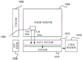
FIG. 12 illustrates another example sensor apparatus for performing aspects of the present disclosure.
FIG. 13 illustrates another example block diagram of a sensing apparatus for performing CV operations.
Fig. 14 is an example flow diagram in accordance with certain aspects of the present disclosure.
FIG. 15 illustrates an example implementation of circuitry and modules for a sensor according to certain aspects of the present disclosure.
FIG. 16A provides an example implementation of an SRAM cell that can be used in aspects of the present disclosure.
FIG. 16B provides an example implementation of a comparator that can be used in aspects of the present disclosure.
FIG. 17 illustrates another example implementation of a sensor apparatus for performing certain aspects of the present disclosure.
FIG. 18 illustrates another example implementation of a sensor apparatus for performing certain aspects of the present disclosure.
Fig. 19 illustrates an example of a computing system in which one or more embodiments may be implemented.
Disclosure of Invention
The present invention relates generally to enabling computer vision, and more particularly to using computer vision to improve the efficiency of detecting features.
In one aspect, techniques are provided for triggering events based on detecting changes in Computer Vision (CV) features, such as edges, corners, etc., by generating computed results based on sensor readings. In another aspect, techniques are also provided for detecting a CV feature when an event is detected based on a change in sensor readings of a sensor element. In certain aspects, the event detection logic and the feature calculation CV operations may be performed individually or in combination in circuitry on the sensor or in software/firmware on the computing device.
An example vision sensor may include a sensor element array including a plurality of sensor elements arranged along at least a first dimension and a second dimension of the sensor element array, each of the plurality of sensor elements capable of producing a sensor reading based on light incident on the sensor element. Further, the vision sensor may include dedicated Computer Vision (CV) calculation hardware configured to calculate a local CV feature of the subject sensor element based at least on sensor readings of the subject sensor element and neighboring sensor elements of the subject sensor element, and generate an event based on a change in the calculated CV feature of the subject sensor element from a previously calculated CV feature, the event comprising information relating to a location of the subject sensor element associated with the change in the calculated CV feature.
In certain aspects of the invention, dedicated CV computation hardware may be implemented as dedicated CV processing modules, in-pixel circuitry, or peripheral circuitry. The pixel may contain a sensor element and in-pixel circuitry. In some cases, events generated at dedicated CV computation hardware may be sent to the application processor. Computing the local CV features may include generating a Local Binary Pattern (LBP) flag, a variant of the LBP flag, or a signed gradient Histogram (HSG) flag. In some cases, a sensor element of the sensor element array may include at least one photodiode. In some aspects of the invention, events may be generated using Dynamic Visual Sensor (DVS) circuitry.
Aspects of the invention further disclose methods and apparatus comprising means for performing the aspects disclosed above and disclosed throughout this specification. Aspects of the invention further disclose non-transitory computer-readable storage media, wherein the non-transitory computer-readable storage media may include instructions executable by a special purpose computer vision microprocessor for performing aspects of the invention discussed above and throughout this specification.
The foregoing has outlined rather broadly the features and technical advantages of the examples in order that the detailed description that follows may be better understood. Additional features and advantages will be described hereinafter. The conception and specific examples disclosed may be readily utilized as a basis for modifying or designing other structures for carrying out the same purposes of the present invention. Such equivalent constructions do not depart from the spirit and scope of the appended claims. The features which are believed to be characteristic of the concepts disclosed herein, both as to their organization and method of operation, together with the advantages associated therewith, will be better understood from the following description when considered in connection with the accompanying figures. Each of the figures is provided for purposes of illustration and description only and is not provided as a definition of the limits of the claims.
Detailed Description
Several illustrative embodiments will now be described with respect to the accompanying drawings, which form a part hereof. While specific embodiments in which one or more aspects of the invention may be implemented are described below, other embodiments may be used and various modifications may be made without departing from the scope of the invention or the spirit of the following claims.
The sensor may comprise a sensor element array of a plurality of sensor elements. The sensor element array may be a 2-dimensional array including sensor elements arranged in two dimensions (e.g., columns and rows) of the sensor element array. Each of the sensor elements may be capable of generating a sensor reading based on an environmental condition. In certain implementations, the sensor can be a visual sensor and can generate sensor readings based on light incident on the sensor element. FIG. 1 illustrates an example sensor 100 including a plurality of sensor elements arranged in a 2-dimensional array. In fig. 1, the illustration of sensor 100 represents 64(8 × 8) sensor elements in an array of sensor elements. In various implementations, the shape of the sensor elements, the number of sensor elements, and the spacing between the sensor elements may vary greatly without departing from the scope of the present invention. Sensor element 102 represents an example sensor element from a grid of 64 sensor elements.
In certain implementations, the sensor elements may have dedicated Computer Vision (CV) computing hardware implemented as in-pixel circuitry (computing structure) coupled to the sensor elements. In some implementations, the sensor elements and in-pixel circuitry together can be referred to as pixels. The processing performed by the in-pixel circuitry coupled to the sensor elements may be referred to as in-pixel processing. In some cases, the array of sensor elements may be referred to as a pixel array, with the difference that the pixel array includes both sensor elements and in-pixel circuitry associated with each sensor element. Fig. 2 illustrates an example pixel 200 having a sensor element 202 and in-pixel circuitry 204. In some embodiments, the in-pixel circuitry 204 may be analog circuitry, digital circuitry, or any combination thereof.
In certain implementations, the sensor element array can have dedicated CV computation hardware implemented as peripheral circuitry (computation structure) coupled to a set of sensor elements. This peripheral circuit may be referred to as an on-chip sensor circuit. FIG. 3 illustrates example peripheral circuitry (304 and 306) coupled to an array of sensor elements 302.
Further, as shown in fig. 4, in certain embodiments, the sensor element array may have dedicated CV computation hardware implemented as a dedicated CV processing module 404 coupled to the sensor element array 402 and implemented using an Application Specific Integrated Circuit (ASIC), a Field Programmable Gate Array (FPGA), an embedded microprocessor, or any similar analog or digital computation logic for performing aspects of the invention. In certain implementations, dedicated CV computation hardware implemented as a dedicated CV processing module 404 may be configured to execute instructions stored on a non-transitory computer media device for computing CV features.
It should be noted that, at least in some embodiments, the dedicated CV processing module 404 is in addition to the application processor 406, rather than replacing the application processor 406. For example, the dedicated CV processing module 404 may process and/or detect CV features. The application processor 406 may receive indications of these detected CV features and pattern matches against previously stored images or reference indications to determine macroscopic features such as smiles, faces, objects, and the like. Further, the application processor 406 may be relatively much more complex, computationally intensive, power intensive, and responsible for performing system-level operations (e.g., an operating system), implementing a user interface for interacting with a user, performing power management of the device, managing memory and other resources, and so forth. The application processor 406 may be similar to the processor 1910 of fig. 19.
FIG. 5 illustrates an example implementation for a sensing apparatus including a vision sensor. Several techniques may be employed for acquiring an image or a series of images, such as a video, using one or more cameras coupled to a computing device.
FIG. 5 illustrates an example implementation of a visual sensor using an event-based camera. The vision sensor may be used in a camera or a video camera for acquiring image data. The event-based camera sensor may be configured to acquire image information based on the event. In one embodiment, as shown in fig. 1, an event-based camera may include a plurality of pixels. Each pixel may include a sensor element and in-pixel circuitry. Each pixel may be configured to acquire image data based on an event detected at the pixel. For example, in one embodiment, a change in the perceived environmental conditions at any given pixel (e.g., a change in light reflected off an object) may cause a voltage change that exceeds a threshold value, and may cause an event at the pixel. In response to the event, logic associated with the pixel may send the sensor read to a processor for further processing.
Referring to fig. 6, each pixel may contain a photodiode 602 and a Dynamic Vision Sensor (DVS)604 circuit. The DVS module may also be referred to as an event detection module. The event detection module detects a change in value at the pixel and generates an event indicator. When the intensity change of the pixel exceeds a threshold, a sensor read is issued to the processor, indicating an event. In some cases, the location of the sensor element that detected the event is sent along with the payload to a computer system for further processing. In one embodiment, the payload may be the voltage strength, the change in voltage strength, or the polarity (sign) of the change in voltage strength. In some cases, an event-based camera may result in a greatly reduced amount of data being passed to the processor for further processing, which results in power savings, as compared to a conventional frame-based camera.
Referring back to FIG. 5, block 502 generally represents a sensor and event detection circuit. Block 502 represents a sensor having a plurality of pixels, each pixel including a sensor element and circuitry for detecting an event. Each pixel uses a sensor element to generate a sensor reading. The sensor readings are later digitized, i.e., converted from analog to digital data using ADC converter 508. In one embodiment, for each pixel, the results of the previous sensor readings may be stored in the column parallel SRAM 506. In some cases, the results stored in the column parallel SRAM 506 may be used by a comparator to compare and trigger events based on a comparison between the current sensor reading and a previous sensor reading. Analog information acquired at the pixels is converted to the digital domain using an analog-to-digital (ADC) converter 508. The digitized sensor readings may be sent to processor 512 for further image processing to calculate CV features.
The image processor 512 may compute certain CV features on the information received from the individual pixels for detecting the features and thus the objects associated with those features. The features may comprise less complex features such as edges, corners, etc. The calculation of the CV features may use information from a plurality of pixels of the sensor element array for detecting the features by performing a multi-pixel calculation. For example, to calculate the CV features of a subject sensor element or pixel, the CV operation may use sensor readings generated by neighboring sensor elements or pixels in proximity to the subject sensor element or pixel.
In certain embodiments, on an application processor 406, such as the image processor 512, computing lower-level CV features, such as Linear Binary Patterns (LBPs), variants of LBPs, and signed gradient Histogram (HSG) labels, may be power-intensive and processing-intensive. In many cases, an event detected at the pixel level may falsely cause a chain of events until the change is discarded by performing a CV operation on the pixel values at the application processor 406. Furthermore, converting analog pixel values to digital pixel values may consume power. Furthermore, detecting CV features on the application processor 406 may be power and processing intensive, as performing CV operations on the application processor 406 in many cases requires storing information from sensors in system memory, triggering processing of sensor information, fetching instructions from memory for CV calculations, and storing results. In addition, the application processor 406 is typically power hungry when executing instructions. Spurious or non-interesting events from the sensors wake up the application processor 406 that may be running in a low power mode due to inactivity and greatly increase the power consumption of the system.
Certain embodiments of the present invention describe techniques for performing events based on CV operations (e.g., LBP, variants of LBP, and HSG flag computation using dedicated CV computation hardware) rather than waking the application processor 406 and computing these low-level CV features at the application processor 406.
In some cases, events may be detected at a feature-level granularity rather than a pixel-level granularity by executing CV operations for detecting CV features inside or very close to the pixels by dedicated CV computation hardware. Detecting events at the feature level granularity may reduce the number of false positive events generated and send them to the application processor 406 for further processing.
As described herein, the dedicated CV computation hardware computes a CV feature or localized CV feature for each of the subject sensor elements based at least in part on signals associated with a plurality of neighboring sensor elements that are proximate to the subject sensor element.
As described herein, sensor elements that are relatively close to a subject sensor element may be referred to as neighboring sensor elements. In certain aspects of the present disclosure, adjacent sensor elements may include sensor elements that are immediately adjacent to the subject sensor element. In certain other aspects of the present disclosure, neighboring sensor elements may also include sensor elements that are relatively close to, but not immediately adjacent to, the subject sensor element. For example, in some cases, when the width or height of the number of sensors is sixty-four sensor elements, sensor elements within three sensor elements from the subject sensor element may still be considered neighboring sensor elements.
As described herein, a CV feature or localized CV feature may refer to detecting a low-level CV mark or indicator, such as a marker associated with each sensor element or pixel of a sensor. For example, the label may comprise an LBP label of the sensor element. The LBP label of a sensor element may be generated by comparing sensor readings of the sensor element and some neighboring sensor elements of the sensor element. The LBP flag may indicate whether the CV feature from the reference of the sensor element represents an edge, a corner, a curve, a blob, or the like. Other techniques, such as HSG or other suitable variants of LBP, may be used to detect CV features without departing from the scope of the invention.
As described herein, detecting and/or generating an event based on a change in CV characteristics may refer to detecting a change in characteristics from an angle of a sensor element or a small group of sensor elements. For example, if the LBP label at the sensor element changes, an event may be detected and/or generated. In other words, if the CV feature detected at the sensor element changes from a blob to an edge, this may trigger the generation of an event.
In addition to the LBP markers discussed herein, different types of CV features may also include calculating variants of LBP markers. Such a variant may Comprise (CS) -LBP, where the central pixel/block is not considered, and all the opposite corners/edges around the central block are compared, and thus 4 comparison markers are generated, which then represent the LBP markers and are used in the same way as the previously described LBP. Other variations include, but are not limited to, "patch symmetric" LBP (where the center pixel/block is not considered in the comparison, but the average of the entire 3x3 patch is calculated, and then each edge/corner is compared to the average) and "Local Ternary Patterns (LTP)" (variants of LBP that contain not only 1 or 0 but may contain results of +1, 0, and-1; zero means the difference is below the threshold, and +1 and-1 means the difference is greater than the threshold and also considers whether the difference is a sign difference).
As described in more detail below, the generation of events with additional information (e.g., location and CV characteristic information) may be provided to an application processor for further processing. In one aspect of the invention, the application processor may use these events and associated information for detecting macroscopic features such as smiles, faces, or any other object used for the matter.
FIG. 7 illustrates an example block diagram of a sensing device for calculating and detecting CV characteristics based on detected events. Fig. 7 illustrates a sensor 702, an event detection module 704, and a CV module 706. As shown in fig. 7, after generating sensor readings from sensor 702, event detection module 704 may detect an event based on a change in the sensor readings. Once an event representing a change in pixel values is detected, the CV module may calculate CV features and detect the event at a feature level granularity. In some cases, after detecting a feature, an application executing on the processor may use the detected feature.
The sensors 702, event detection module 704, and CV module 706 may be implemented in various different configurations at various different granularities. For example, the sensor in fig. 7 may represent a single sensor element (e.g., sensor element 102 in fig. 1) or an entire array of sensor elements (e.g., sensor 100 in fig. 1). In certain embodiments, the event detection module 704 or/and the CV module 706 may be implemented in analog or digital form in the in-pixel circuitry 204, the peripheral circuitry 304/306, or the dedicated CV processing module 404.
The event detection module 704 may be implemented as an in-pixel circuit or a peripheral circuit, or any combination thereof. In configurations where event detection module 704 processes sensor readings for multiple pixels, event detection module 704 can process sensor readings from sensor elements associated with one dimension of the sensor element array (e.g., a column (also referred to as a column-parallel DVS)) or the entire sensor element array.
The CV module 706 may be implemented as in-pixel circuitry internal to each of the sensor pixels 204, as peripheral circuitry 304 for processing sensor readings for multiple pixels, or as a dedicated CV processing module 404, as on-chip or off-chip sensor circuitry, or any combination thereof. In configurations where the CV module 706 processes sensor readings for a plurality of pixels, the CV module 706 may process sensor readings from sensor elements associated with one dimension of an array of sensor elements (e.g., a column (also referred to as a column-parallel CV)) or the entire array of sensor elements. In some embodiments, CV module 706 may be implemented in firmware/software instructions for execution on a dedicated CV processing module 404 in the digital domain.
Although not shown, CV module 706 may be configured to perform analog or digital operations representing multi-pixel calculations of sensor elements based on sensor readings generated by neighboring sensor elements in proximity to a reference sensor element.
Fig. 8 is an example flow diagram in accordance with certain aspects of the present disclosure. Some or all of process 800 (or any other process described herein or variations and/or combinations thereof) may be performed by circuitry or logic. The circuitry or logic may be implemented in-pixel circuitry, peripheral circuitry, or a dedicated CV processing module, or any combination thereof. In some cases, all or part of the logic may be implemented using instructions executed on digital circuits and stored on a non-transitory computer-readable storage medium.
At block 802, a component of a sensor array element, such as a subject sensor element, receives at least one sensor reading based on light incident on the subject sensor element. The sensor element array includes a plurality of sensor elements. The sensor elements may be arranged at least along a first dimension and a second dimension of the array of sensor elements. In certain aspects of the present disclosure, the array of sensor elements is a vision sensor, and each of the sensor elements includes a photodiode.
At block 804, a component disclosed herein, such as dedicated CV computation hardware, detects a change in sensor readings of the subject sensor elements and generates an event. In certain embodiments, an event detection circuit or DVS module is used to detect and generate events.
At block 806, a component disclosed herein, such as dedicated CV computation hardware, computes localized CV features based on sensor readings of the subject sensor element and neighboring sensor elements of the subject sensor element.
As described herein, a CV feature or localized CV feature may refer to a low-level CV flag or indicator, such as a flag associated with each sensor element or pixel of a sensor. For example, the label may comprise an LBP label of the sensor element. The LBP label of a sensor element may be generated by comparing sensor readings of the sensor element and some neighboring sensor elements of the sensor element. The LBP flag may indicate whether the CV feature from the reference of the sensor element represents an edge, a corner, a curve, a blob, or the like. Other techniques, such as HSG or other suitable variants of LBP, may be used to detect CV features without departing from the scope of the invention. Localized CV features can be inferred from either LBP markers or HSG markers.
In certain aspects of the invention, the dedicated CV computation hardware is implemented as part of a dedicated CV microprocessor, such as the dedicated CV processing module 404 in fig. 4. In certain other aspects of the invention, dedicated CV computation hardware may be implemented as either the in-pixel circuitry 204 or the peripheral circuitry 304. In some aspects of the invention, the computed CV features are sent from the dedicated CV computation hardware to the application processor 406 for further processing.
It should be appreciated that the particular steps illustrated in FIG. 8 provide a particular method of switching between operational modes according to one embodiment. Other sequences of steps may also be performed in alternative embodiments. For example, alternative embodiments may perform the steps/blocks outlined above in a different order. For example, the user may select to change from the third mode of operation to the first mode of operation, from the fourth mode to the second mode, or any combination therebetween. Moreover, the individual steps/blocks illustrated in fig. 8 may include multiple sub-steps performed in various orders as applicable to the individual steps. Moreover, additional steps/blocks may be added or removed depending on the particular application. Many variations, modifications, and alternatives to the processes described will be recognized and understood by those of ordinary skill in the art.
Fig. 9, 10, 11, and 12 are example configurations for performing a DVS operation prior to performing a CV operation as described with respect to fig. 7 and 8.
Fig. 9 illustrates example information transmitted between the event detection module 704 and the CV module 706 in fig. 7. In one embodiment, the DVS module 901 detects events associated with the position of the sensor elements at the sensor element array 900. The DVS module 901 may promote the events and information 906 to the CV module 903, including the locations of the sensor elements at the array of sensor elements and the optional payload. The payload may contain the voltage strength, a change in the voltage strength, or a polarity of the change.
The event or the location of the sensor element associated with the event may correspond to an image pixel of image 904. The CV module 903 may access a set of image pixel values 902 that includes neighboring values of the image pixels in which the event was detected, such that a CV feature may be detected for the set of pixels, rather than re-calculating the CV feature set for the entire image 904. In one embodiment where the CV feature is detected in the circuit, the value of the neighboring pixel may be accessed from the previous value held in the capacitor of the neighboring pixel. In another embodiment, where CV module 903 operates in a computing system, the neighboring values may be retrieved from memory from the stored images.
FIG. 10 illustrates an example pixel for performing aspects of the disclosure. The pixel in fig. 10 includes a sensing circuit 1002 (i.e., photodiode) and DVS and/or CV circuits 1004 for analog or digital processing in the pixel. As shown in fig. 10, in certain embodiments, multiple capacitors may be used to store the previous voltage (V _ PRE) and the current (V _ CUR) voltage. The CV block 1004 may calculate LBP markers, variants of LBP markers, or HSG markers for CV feature detection. The output may contain information indicative of an aspect of CV feature detection as well as information indicative of an event from an event detection module. For example, in one aspect of the present invention, the output may include 3-4 bits of information regarding detection of a CV (i.e., LBP or HSG) feature and another bit of information for the occurrence of the event itself.
FIG. 11 illustrates an example sensor device implementing the event detection module 702 for performing aspects of the present disclosure. In fig. 11, each pixel, similar to the pixel discussed in fig. 6, includes a sensor element 602 and an event detection module 604, shown together as block 1104. Block 1106 represents a ROW driver (ROW DRV) for driving the data output of the sensor and block 1108 represents a Timing Controller (TCON). In one embodiment, for each pixel, the results of previous sensor reads may be stored in column parallel SRAM 1112. The results stored in the column parallel SRAM 1112 may be used by a comparator to compare and trigger events based on a comparison between the current sensor reading and a previous sensor reading.
In fig. 11, each pixel may output a digital output from the event detection module that is indicative of the pixel level change and the voltage reading from the sensor element. As shown in fig. 11, in some cases, CV module 1110 may be implemented for a group of pixels or an entire array of sensor elements. CV module 1110 may be implemented as peripheral circuitry 304/306 or as dedicated CV processing module 404. Implementing CV module 1110 for a group of pixels or an entire array of sensor elements may allow for high efficiency in processing data. For example, the same CV module may be capable of servicing different groups of pixels in sequence. In one embodiment, the digital output produced by the event detection module (Dout of DVS) located on the pixel 1102 may indicate a change to the CV circuit, and the processing logic may be selected/triggered to process the voltage output (Vpix) from the pixel.
FIG. 12 illustrates another example sensor apparatus for performing aspects of the disclosure, and is a variation of the example configuration discussed in FIG. 11. For example, similar to fig. 11, fig. 12 has components such as a row driver 1206, a timing controller 1208, and a CV module 1210. In fig. 12, each pixel includes a sensor element. Each pixel, e.g., pixel 1202, outputs a current voltage (current Vpix) and a previous voltage (previous Vpix). The previous voltage may be maintained by the pixel using a capacitor circuit. The event detection module may be implemented as the peripheral circuitry 304 or the dedicated CV processing module 404, rather than for each individual pixel (i.e., the in-pixel circuitry 204). As shown in fig. 12, the event detection module may be implemented as a column-parallel event detection module 1212 for each pixel column. The event detection module 1212 compares the current voltage and the previous voltage output by the pixel and generates an event based on a difference between the current voltage output and the previous voltage. The arbitration circuit 1214 shown in FIG. 12 may provide multiplexing logic for selecting the appropriate column and driving the appropriate data between the column parallel event detection module and the CV module 1210.
FIG. 13 illustrates another example block diagram of a sensing apparatus for calculating CV characteristics. FIG. 13 illustrates a sensor 1302, a CV module 1304, and a DVS module 1306. In contrast to the apparatus described with reference to fig. 7 (and fig. 8 to 12), the CV features in fig. 13 are calculated prior to DVS operations. As shown in fig. 13, after generating sensor readings from the sensors 1302, the CV module 1304 may process the sensor information and detect CV features and communicate the information to the DVS module 1306. DVS module 1306 may thus detect events at CV feature granularity (as opposed to events at pixel granularity). In some cases, after detecting the CV features, the CV module 1304 may send the information to a processor, such as the application processor 406, for further processing.
The sensors 1302, CV modules 1304, and DVS modules 1306 may be implemented in a variety of different configurations at a variety of different granularities. For example, sensor 1302 in fig. 13 may represent a single sensor element (e.g., sensor element 102 in fig. 1) or an entire array of sensor elements (e.g., sensor 100 in fig. 1).
The CV module 1304 may be implemented as in-pixel circuitry internal to each of the sensor pixels, peripheral circuitry for processing sensor readings for multiple pixels, or a dedicated CV processing module, on-chip sensor circuitry. In configurations where the CV module 1304 processes sensor readings for a plurality of sensor elements, the CV module 1304 may process sensor readings from sensor elements associated with one dimension of an array of sensor elements (e.g., a column (also referred to as column-parallel CV)) or the entire array of sensor elements.
Although not shown, the CV module 1304 may be configured to perform analog or digital operations representing multi-pixel calculations of pixels based on sensor readings generated by neighboring sensor elements proximate to a reference pixel.
In some embodiments, CV module 1304 may be implemented in firmware/software instructions for execution on a processor in the digital domain.
Similarly, the DVS module 1306 may be implemented as an in-pixel circuit internal to each of the sensor pixels, a peripheral circuit for processing sensor readings for multiple pixels, an on-chip sensor circuit, or using a dedicated CV processing module. In configurations where the DVS module 1306 processes sensor readings for multiple pixels, the DVS module 1306 may process sensor readings from sensor elements associated with one dimension of the sensor element array (e.g., a column (also referred to as column-parallel DVS)) or the entire sensor element array.
Fig. 14 is an example flow diagram in accordance with certain aspects of the present disclosure. Some or all of process 1400 (or any other process described herein or variations and/or combinations thereof) may be performed by circuitry or logic. The circuits or logic may be implemented in-pixel circuitry, peripheral circuitry, or dedicated CV processing logic, or any combination thereof. In some cases, all or part of the logic may be implemented using instructions executed on digital circuits and stored on a non-transitory computer-readable storage medium.
At block 1402, a component of a sensor array element, e.g., a subject sensor element, receives at least one sensor reading based on light incident on the subject sensor element. The sensor element array comprises a plurality of sensor elements, and the sensor elements are arranged at least along a first dimension and a second dimension of the sensor element array. In certain aspects of the present disclosure, the array of sensor elements is a vision sensor, and each of the sensor elements includes at least one photodiode.
At block 1404, a component disclosed herein, such as dedicated CV computation hardware, computes a localized CV feature, wherein the localized CV feature is based on sensor readings of at least neighboring sensor elements of the subject sensor element.
As described herein, a CV feature or localized CV feature may refer to a low-level CV flag or indicator, such as a flag associated with each sensor element or pixel of a sensor. For example, the label may comprise an LBP label of the sensor element. The LBP label of a sensor element may be generated by comparing sensor readings of the sensor element and some neighboring sensor elements of the sensor element. The LBP flag may indicate whether the CV feature from the reference of the sensor element represents an edge, a corner, a curve, a blob, or the like. Other techniques, such as HSG or other suitable variants of LBP, may be used to detect CV features without departing from the scope of the invention. The localized CV features may be based on LBP markers or HSG markers.
As described herein, sensor elements that are relatively close to a subject sensor element may be referred to as neighboring sensor elements. In certain aspects of the present disclosure, adjacent sensor elements may include sensor elements that are immediately adjacent to the subject sensor element. In certain other aspects of the present disclosure, neighboring sensor elements may also include sensor elements that are relatively close to, but not immediately adjacent to, the subject sensor element. For example, in some cases, when the width or height of the number of sensors is sixty-four sensor elements, sensor elements within three sensor elements from the subject sensor element may still be considered neighboring sensor elements.
In certain aspects of the invention, the dedicated CV computation hardware is implemented as part of a dedicated CV microprocessor, such as the dedicated CV processing module 404 in fig. 4. In certain other aspects of the invention, dedicated CV computation hardware may be implemented as either the in-pixel circuitry 204 or the peripheral circuitry 304.
At block 1406, a component disclosed herein, such as dedicated CV computation hardware, generates an event based on the change in the computed CV features, the event including information relating to the position of the subject sensor element associated with the change in the computed CV features. In some aspects of the invention, the computed CV characteristics are sent from dedicated CV computation hardware to the application microprocessor.
As described herein, generating an event based on a change in a CV feature may refer to detecting a change in the feature from the perspective of a sensor element or a small group of sensor elements. For example, if the LBP label at the sensor element changes, an event may be detected and/or generated. In other words, if the CV feature detected at the sensor element changes from a blob to an edge, this may trigger the generation of an event.
The generated events with additional information, such as location and CV feature information, may be provided to the application processor for further processing. In one aspect of the invention, the application processor may use these events and associated information for detecting macroscopic features such as smiles, faces, or any other object used for the matter.
It should be appreciated that the particular steps illustrated in FIG. 14 provide a particular method of switching between operational modes, according to one embodiment. Other sequences of steps may also be performed in alternative embodiments. For example, alternative embodiments may perform the steps/blocks outlined above in a different order. For example, the user may select to change from the third mode of operation to the first mode of operation, from the fourth mode to the second mode, or any combination therebetween. Moreover, a single step/block illustrated in fig. 14 may include multiple sub-steps performed in various orders as applicable to individual steps. Moreover, additional steps/blocks may be added or removed depending on the particular application. Many variations, modifications, and alternatives to the processes described will be recognized and understood by those of ordinary skill in the art.
Fig. 15, 17, and 18 are example configurations of computing CV features prior to performing DVS operations as described with respect to fig. 13.
FIG. 15 illustrates an example implementation of circuitry and modules for a sensor according to certain aspects of the present disclosure. As shown in fig. 15, a pixel 1502 may include a sensing circuit 1504 (e.g., a photodiode) and a CV circuit 1506. The event detection module may be implemented as an on-chip sensor circuit and includes column parallel circuitry (SRAM 1508 and comparator 1510) for checking for time differences between any two frames. Although an SRAM cell 1508 is shown in FIG. 15, any other type of volatile or non-volatile memory may be used. In a digital implementation of the event detection module, the analog capacitor may be replaced by a digital buffer and the analog comparator may be replaced by a digital comparator.
FIG. 16A provides an example implementation of a Static Random Access Memory (SRAM) cell that may be used in the event detection module described in FIG. 15 and other figures of the present disclosure. As with the bistable self-locking circuit shown in fig. 16A, M1, M2, and M5 form one pair of bistable self-locking circuits, and M3, M4, M6 form a second pair of bistable self-locking circuits. FIG. 16B provides an example implementation of a comparator for comparing previous and current values in the event detection module in FIG. 15 and other figures of the present invention. The comparator may compare the two voltages or currents and output a digital signal indicating which of the two values is larger (or smaller). The comparator shown in fig. 16B is a voltage comparator.
FIG. 17 illustrates another example implementation of a sensor apparatus 1702 for performing certain aspects of the present disclosure. As shown in fig. 17, the CV module 1706 and event detection circuitry are both implemented inside the pixel and are configured to perform intra-pixel CV and DVS processing. The CV module may generate either an LBP marker or an HSG marker. In fig. 17, the CV operation is performed first, followed by the DVS operation. DVS operations may be performed in the digital domain and events may be generated based on feature detection. The event detection circuit may implement SRAM 1708 or a similarly suitable memory for storing the previous CV output. The previous and current CV outputs may be compared by comparator 1710 for generating DVS events. The DVS signature events and CV information may be provided to the application processor 406 for further processing.
FIG. 18 illustrates another example implementation of a sensor apparatus 1802 for performing certain aspects of the present disclosure. As shown in fig. 18, sensing circuitry 1804 (e.g., photodiodes) and CV modules 1806 are implemented inside the sensor device 1802 (i.e., pixels) and detect CV features within the pixels. The event detection module is implemented as an on-chip sensor circuit and in a column parallel circuit. In fig. 18, the CV operation is performed first, followed by the DVS operation. DVS operations may be performed in the digital domain and events may be generated based on feature detection. The event detection module may implement SRAM 1808 or similarly suitable memory for storing previous CV outputs. The previous and current CV outputs may be compared by comparator 1810 for generating DVS events. The DVS signature events and CV information may be provided to a processor for further processing.
Although many of the examples described above disclose performing DVS (i.e., event detection) and CV operations in circuitry, in some embodiments, one or both of those operations may be performed in software or firmware on a processor in the digital domain without departing from the scope of the present invention. For example, in some embodiments, these operations may be performed in the digital domain in the dedicated CV processing module 404.
According to one or more aspects, any and/or all of the apparatus modules, circuits, methods, and/or method steps described in fig. 1-18 herein may be implemented by and/or in a sensor apparatus, such as a visual sensor apparatus. In one embodiment, one or more of the method steps discussed may be implemented by sensing elements and processing logic of a sensor device, such as a CV circuit, an event detection module, or any other circuit. Additionally or alternatively, any and/or all of the methods and/or method steps described herein may be embodied in computer readable instructions, such as computer readable instructions stored on a computer readable medium (e.g., memory, storage device, or another computer readable medium).
FIG. 19 illustrates an example computing device incorporating portions of a device and sensor 100 employed in practicing embodiments of the invention. For example, computing device 1900 may represent some of the components of a mobile device or any other computing device. Examples of computing device 1900 include, but are not limited to, a desktop computer, workstation, personal computer, supercomputer, video game console, tablet computer, smart phone, laptop computer, netbook, or other portable device. Fig. 19 provides a schematic illustration of one embodiment of a computing device 1900 that can perform the methods provided by various other embodiments as described herein and/or can function as a host computing device, a remote query kiosk/terminal, a point-of-sale device, a mobile multifunction device, a set-top box, and/or a computing device. FIG. 19 is intended merely to provide a generalized illustration of various components, any or all of which may be utilized as desired. Thus, FIG. 19 broadly illustrates how individual system elements may be implemented in a relatively separated or relatively more integrated manner.
The computing device 1900 may include software elements shown as currently located within a working memory 1935, including an operating system 1940, device drivers, executable libraries, and/or other code, such as one or more application programs 1945, which may include computer programs provided by various embodiments and/or which may be designed to implement methods and/or configure systems, provided by other embodiments, as described herein. By way of example only, one or more programs described with respect to the methods discussed above may be implemented as code and/or instructions executable by a computer (and/or a processor within a computer); in an aspect, such code and/or instructions may then be used to configure and/or adapt a general purpose computer (or other device) to perform one or more operations in accordance with the described methods.
The set of such instructions and/or code may be stored on a computer-readable storage medium, such as the storage 1925 described above. In some cases, the storage medium may be incorporated within a computing device, such as computing device 1900. In other embodiments, the storage medium may be separate from the computing device (e.g., a removable medium such as a compact disc), and/or provided in an installation package, such that the storage medium may be used to program, configure and/or adapt a general purpose computer having the instructions/code stored thereon. These instructions may be in the form of executable code that is executable by computing device 1900, and/or may be in the form of source and/or installable code that, after being compiled on computing device 1900 and/or installed on computing device 1900 (e.g., using any of a variety of commonly available compilers, installation programs, compression/decompression utilities, etc.), is then in the form of executable code.
Substantial changes may be made depending on the specific requirements. For example, customized hardware might also be used and/or particular elements might be implemented in hardware, software (including portable software, e.g., applets, etc.), or both. In addition, connections to other computing devices 1900, such as network input/output devices, may be employed.
Some embodiments may employ a computing device (e.g., computing device 1900) to perform a method in accordance with the invention. For example, some or all of the procedures of the described methods may be performed by the computing device 1900 in response to the processor 1910 executing one or more sequences of one or more instructions (which may be incorporated into the operating system 1940 and/or other code, such as an application 1945) contained in the working memory 1935. Such instructions may be read into the working memory 1935 from another computer-readable medium, such as one or more of the storage devices 1925. For example only, execution of the sequences of instructions contained in the working memory 1935 may cause the processor 1910 to perform one or more procedures of the methods described herein.
As used herein, the terms "machine-readable medium" and "computer-readable medium" refer to any medium that participates in providing data that causes a machine to operation in a specific fashion. In an embodiment implemented using computing device 1900, various computer-readable media may involve providing instructions/code to processor 1910 for execution and/or possibly for storing and/or carrying such instructions/code (e.g., as signals). In many implementations, the computer-readable medium is a physical and/or tangible storage medium. Such a medium may take many forms, including but not limited to, non-volatile media, and transmission media. Non-volatile media includes, for example, optical and/or magnetic disks, such as the storage device 1925. Volatile media includes, but is not limited to, dynamic memory, such as working memory 1935. Transmission media includes, but is not limited to, coaxial cables, copper wire and fiber optics, including the wires that comprise bus 1905, as well as the various components of communication subsystem 1930 (and/or the media by which communication subsystem 1930 provides communication with other devices). Thus, transmission media can also take the form of waves (including, but not limited to, radio, acoustic and/or light waves, such as those generated during radio wave and infrared data communications). In alternative embodiments, event driven components and devices (e.g., cameras) may be used, where some of the processing may be performed in the analog domain.
Common forms of physical and/or tangible computer-readable media include, for example, a floppy disk, a flexible disk, hard disk, magnetic tape, or any other magnetic medium, a CD-ROM, any other optical medium, punch cards, paper tape, any other physical medium with patterns of holes, a RAM, a PROM, an EPROM, a flash EPROM, any other memory chip or cartridge, a carrier wave as described hereinafter, or any other medium from which a computer can read instructions and/or code.
Various forms of computer readable media may be involved in carrying one or more sequences of one or more instructions to processor 1910 for execution. By way of example only, the instructions may initially be carried on a magnetic and/or optical disk of a remote computer. The remote computer can load the instructions into its dynamic memory and send the instructions as signals over a transmission medium to be received and/or executed by the computing device 1900. According to various embodiments of the invention, such signals, which may be in the form of electromagnetic signals, acoustic signals, optical signals, and/or the like, are examples of carrier waves on which instructions may be encoded.
The communication subsystem 1930 (and/or its components) typically receives the signals, and the bus 1905 then possibly carries the signals (and/or data, instructions, etc. carried by the signals) to a working memory 1935, from which the processor 1910 retrieves and executes the instructions. The instructions received by the working memory 1935 may optionally be stored on non-transitory storage 1925 either before or after execution by the processor 1910.
The methods, systems, and devices discussed above are examples. Various embodiments may omit, replace, or add various procedures or components as desired. For example, in alternative configurations, the described methods may be performed in an order different than described, and/or stages may be added, omitted, and/or combined. Also, features described with respect to certain embodiments may be combined in various other embodiments. Different aspects and elements of the embodiments may be combined in a similar manner. Also, technology evolves and, thus, many of the elements are examples, which do not limit the scope of the disclosure to those specific examples.
Specific details are given in the description to provide a thorough understanding of the embodiments. However, embodiments may be practiced without these specific details. For example, well-known circuits, processes, algorithms, structures, and techniques have been shown without unnecessary detail in order to avoid obscuring the embodiments. This description provides example embodiments only, and is not intended to limit the scope, applicability, or configuration of the invention. Indeed, the previous description of the embodiments will provide those skilled in the art with a heuristic description for implementing an embodiment of the invention. Various changes may be made in the function and arrangement of elements without departing from the spirit and scope of the invention.
Also, some embodiments are described as a process that is depicted in flowchart or block diagram form. Although each flowchart or block diagram may describe the operations as a sequential process, many of the operations can be performed in parallel or concurrently. Further, the order of the operations may be rearranged. The process may have additional steps not included in the figure. Furthermore, embodiments of the methods may be implemented by hardware, software, firmware, middleware, microcode, hardware description languages, or any combination thereof. When implemented in software, firmware, middleware or microcode, the program code or code segments to perform the associated tasks may be stored in a computer readable medium such as a storage medium. The processor may perform the associated tasks.
Having described several embodiments, various modifications, alternative constructions, and equivalents may be used without departing from the spirit of the invention. For example, the above elements may simply be components of a larger system, where other rules may take precedence over or otherwise modify the application of the invention. Also, several steps may be performed before, during, or after the above elements are considered. Accordingly, the above description does not limit the scope of the invention.
Claims (18)
1. A computer vision computing method, comprising:
comparing a previous local CV feature computed using computer vision CV feature computation hardware associated with a subject sensor element of an array of sensor elements to a current local CV feature computed using the CV feature computation hardware associated with the subject sensor element, wherein for the previous local CV feature and the current local CV feature the CV feature computation hardware computes the respective CV feature using respective readings from the subject sensor element and respective readings from sensor elements adjacent to the subject sensor element, and wherein:
the sensor element array comprising a plurality of sensor elements arranged along at least a first dimension and a second dimension of the sensor element array,
the pixel comprises the subject sensor element and in-pixel circuitry, an
The CV feature computation hardware is implemented as part of the in-pixel circuitry;
generating an event associated with the subject sensor element based on the comparison, the event comprising a position of the subject sensor element and a feature payload comprising a plurality of bits representing the calculated current local CV feature associated with the subject sensor element; and
sending the event to a processor.
2. The method of claim 1, wherein the localized CV features comprise a Local Binary Pattern (LBP) marker or a variant of the LBP marker.
3. The method of claim 1, wherein the localized CV features comprise signed histogram of gradients (HSG) markers.
4. The method of claim 1, wherein the sensor element array is a vision sensor and each of the plurality of sensor elements of the sensor element array includes at least one photodiode.
5. The method of claim 1, wherein the event is generated using a Dynamic Visual Sensor (DVS) circuit.
6. A vision sensor, comprising:
a sensor element array comprising a plurality of sensor elements arranged along at least a first dimension and a second dimension of the sensor element array, each of the plurality of sensor elements capable of producing a sensor reading based on light incident on the sensor element;
computer vision CV feature computation hardware configured to:
calculating a previous local CV feature associated with a subject sensor element of the array of sensor elements and a current local CV feature associated with the subject sensor element, wherein for the previous local CV feature and the current local CV feature, the CV feature calculation hardware calculates the respective CV features using respective readings from the subject sensor element and respective readings from sensor elements adjacent to the subject sensor element, and wherein:
the pixel comprises the subject sensor element and in-pixel circuitry, an
The CV feature computation hardware is implemented as part of the in-pixel circuitry;
a comparator configured to compare a previous local CV feature associated with the subject sensor element to a current local CV feature associated with the subject sensor element; and
the CV feature calculation hardware is further configured to generate an event associated with the subject sensor element based on the comparison by the comparator, the event comprising a position of the subject sensor element and a feature payload comprising a plurality of bits representing the calculated current local CV feature associated with the subject sensor element, and send the event to a processor.
7. The vision sensor of claim 6, wherein the localized CV features comprise a Local Binary Pattern (LBP) marker or a variant of the LBP marker.
8. The vision sensor of claim 6, wherein the localized CV features comprise signed histogram of gradients (HSG) markers.
9. The vision sensor of claim 6, wherein each of the plurality of sensor elements of the sensor element array comprises at least one photodiode.
10. The vision sensor of claim 6, wherein the events are generated using a Dynamic Vision Sensor (DVS) circuit.
11. A computer vision computing device, comprising:
means for comparing a previous local CV feature computed using computer vision CV feature computation hardware associated with a subject sensor element of an array of sensor elements to a current local CV feature computed using the CV feature computation hardware associated with the subject sensor element, wherein for the previous local CV feature and the current local CV feature, the CV feature computation hardware computes the respective CV features using respective readings from the subject sensor element and respective readings from sensor elements adjacent to the subject sensor element, and wherein:
the sensor element array comprising a plurality of sensor elements arranged along at least a first dimension and a second dimension of the sensor element array,
the pixel comprises the subject sensor element and in-pixel circuitry, an
The CV feature computation hardware is implemented as part of the in-pixel circuitry;
means for generating an event associated with the subject sensor element based on the comparison, the event comprising a location of the subject sensor element and a feature payload comprising a plurality of bits representing the calculated current local CV feature associated with the subject sensor element; and
means for sending the event to a processor.
12. The apparatus of claim 11, wherein the localized CV features comprise a local binary pattern LBP marker or a variant of the LBP marker.
13. The apparatus of claim 11, wherein the localized CV features comprise signed gradient Histogram (HSG) labels.
14. The apparatus of claim 11, wherein the array of sensor elements is a vision sensor and each of the plurality of sensor elements in the array of sensor elements comprises at least one photodiode.
15. A non-transitory computer-readable storage medium, wherein the non-transitory computer-readable storage medium comprises instructions executable by a special-purpose computer vision, CV, processing module for:
comparing a previous local CV feature computed using CV feature computation hardware associated with a subject sensor element of an array of sensor elements to a current local CV feature computed using the CV feature computation hardware associated with the subject sensor element, wherein for the previous local CV feature and the current local CV feature, the CV feature computation hardware computes the respective CV feature using respective readings from the subject sensor element and respective readings from sensor elements adjacent to the subject sensor element, and wherein:
the sensor element array comprising a plurality of sensor elements arranged along at least a first dimension and a second dimension of the sensor element array,
the pixel comprises the subject sensor element and in-pixel circuitry, an
The CV feature computation hardware is implemented as part of the in-pixel circuitry;
generating an event associated with the subject sensor element based on the comparison, the event comprising a position of the subject sensor element and a feature payload comprising a plurality of bits representing the calculated current local CV feature associated with the subject sensor element; and
sending the event to a processor.
16. The non-transitory computer-readable storage medium of claim 15, wherein the localized CV features comprise a local binary pattern LBP marker or a variant of the LBP marker.
17. The non-transitory computer-readable storage medium of claim 15, wherein the localized CV features comprise signed gradient Histogram (HSG) labels.
18. The non-transitory computer-readable storage medium of claim 15, wherein the sensor element array is a vision sensor and each of the plurality of sensor elements of the sensor element array includes at least one photodiode.
Applications Claiming Priority (5)
| Application Number | Priority Date | Filing Date | Title |
|---|---|---|---|
| US201462057927P | 2014-09-30 | 2014-09-30 | |
| US62/057,927 | 2014-09-30 | ||
| US14/859,146 | 2015-09-18 | ||
| US14/859,146 US10728450B2 (en) | 2014-09-30 | 2015-09-18 | Event based computer vision computation |
| PCT/US2015/052067 WO2016053761A1 (en) | 2014-09-30 | 2015-09-24 | Event based computer vision computation |
Publications (2)
| Publication Number | Publication Date |
|---|---|
| CN106716441A CN106716441A (en) | 2017-05-24 |
| CN106716441B true CN106716441B (en) | 2021-05-25 |
Family
ID=55585868
Family Applications (1)
| Application Number | Title | Priority Date | Filing Date |
|---|---|---|---|
| CN201580050415.2A Active CN106716441B (en) | 2014-09-30 | 2015-09-24 | Event-based computer vision computing |
Country Status (5)
| Country | Link |
|---|---|
| US (1) | US10728450B2 (en) |
| EP (1) | EP3201827A1 (en) |
| JP (1) | JP2017531865A (en) |
| CN (1) | CN106716441B (en) |
| WO (1) | WO2016053761A1 (en) |
Families Citing this family (28)
| Publication number | Priority date | Publication date | Assignee | Title |
|---|---|---|---|---|
| CN114796782A (en) | 2015-12-02 | 2022-07-29 | 费雪派克医疗保健有限公司 | Flow path sensing for flow therapy devices |
| JP6668728B2 (en) | 2015-12-14 | 2020-03-18 | 株式会社リコー | Photoelectric conversion element, image reading device, and image forming device |
| US20180146149A1 (en) * | 2016-11-21 | 2018-05-24 | Samsung Electronics Co., Ltd. | Event-based sensor, user device including the same, and operation method of the same |
| WO2018152214A1 (en) | 2017-02-14 | 2018-08-23 | The Trustees Of The University Of Pennsylvania | Event-based feature tracking |
| CN108574793B (en) * | 2017-03-08 | 2022-05-10 | 三星电子株式会社 | Image processing apparatus configured to regenerate time stamp and electronic apparatus including the same |
| US10516841B2 (en) | 2017-03-08 | 2019-12-24 | Samsung Electronics Co., Ltd. | Pixel, pixel driving circuit, and vision sensor including the same |
| US10855927B2 (en) | 2017-03-08 | 2020-12-01 | Samsung Electronics Co., Ltd. | Event detecting device including an event signal generator and an output signal generator |
| WO2019099337A1 (en) | 2017-11-14 | 2019-05-23 | Kaban Technologies Llc | Event camera-based deformable object tracking |
| US10887535B2 (en) * | 2018-07-18 | 2021-01-05 | The Regents Of The University Of California | Query driven image sensing |
| JP7374111B2 (en) * | 2018-09-28 | 2023-11-06 | ソニーセミコンダクタソリューションズ株式会社 | Solid-state imaging device, control method for solid-state imaging device, and electronic equipment |
| KR20200066962A (en) * | 2018-12-03 | 2020-06-11 | 삼성전자주식회사 | Electronic device and method for providing content based on the motion of the user |
| US10832543B2 (en) | 2019-01-11 | 2020-11-10 | The Chamberlain Group, Inc. | Activity sensor |
| KR102640070B1 (en) * | 2019-01-23 | 2024-02-27 | 애플 인크. | Pixel size reduction method for event-driven sensors |
| EP3693698A1 (en) * | 2019-02-05 | 2020-08-12 | Leica Geosystems AG | Measuring device with event-based camera |
| KR20200115881A (en) * | 2019-03-28 | 2020-10-08 | 삼성전자주식회사 | Dynamic vision sensor configured to calibrate event signals using optical black region and method of operating the same |
| CN112118380B (en) | 2019-06-19 | 2022-10-25 | 北京小米移动软件有限公司 | Camera control method, device, equipment and storage medium |
| CN112311964B (en) * | 2019-07-26 | 2022-06-07 | 华为技术有限公司 | Pixel acquisition circuit, dynamic vision sensor and image acquisition equipment |
| KR20220136997A (en) * | 2020-01-31 | 2022-10-11 | 소니 세미컨덕터 솔루션즈 가부시키가이샤 | Solid-state imaging device and imaging device |
| US11134194B2 (en) * | 2020-02-26 | 2021-09-28 | Himax Technologies Limited | Always-on system with multi-layer power management |
| US11227402B2 (en) | 2020-05-29 | 2022-01-18 | Icatch Technology, Inc. | Velocity measuring device |
| EP3930312B8 (en) * | 2020-06-26 | 2023-10-25 | Alpsentek GmbH | Delta image sensor with digital pixel storage |
| CN116057945A (en) * | 2020-07-10 | 2023-05-02 | 索尼半导体解决方案公司 | Image pickup element and image pickup method |
| CN111770245B (en) * | 2020-07-29 | 2021-05-25 | 中国科学院长春光学精密机械与物理研究所 | Pixel structure of retina-like image sensor |
| ES2947688T3 (en) | 2020-08-14 | 2023-08-16 | Alpsentek Gmbh | Image sensor with configurable pixel circuitry and method |
| CN114095676A (en) * | 2021-11-23 | 2022-02-25 | 深圳锐视智芯科技有限公司 | Difference image sensor with digital pixel storage |
| CN114095678A (en) * | 2021-11-23 | 2022-02-25 | 深圳锐视智芯科技有限公司 | Differential image sensor with external writable digital pixel storage |
| WO2023182049A1 (en) * | 2022-03-23 | 2023-09-28 | ソニーセミコンダクタソリューションズ株式会社 | Image sensor and data structure |
| WO2023186468A1 (en) * | 2022-03-31 | 2023-10-05 | Sony Semiconductor Solutions Corporation | Image sensor including pixel circuits for event detection connected to a column signal line |
Citations (1)
| Publication number | Priority date | Publication date | Assignee | Title |
|---|---|---|---|---|
| US8588555B1 (en) * | 2009-06-12 | 2013-11-19 | Cognitive Electronics, Inc. | Power-efficient sensory recognition processor |
Family Cites Families (49)
| Publication number | Priority date | Publication date | Assignee | Title |
|---|---|---|---|---|
| US5543590A (en) | 1992-06-08 | 1996-08-06 | Synaptics, Incorporated | Object position detector with edge motion feature |
| US6822563B2 (en) | 1997-09-22 | 2004-11-23 | Donnelly Corporation | Vehicle imaging system with accessory control |
| JPH0799646A (en) | 1993-05-31 | 1995-04-11 | Sony Corp | Hierarchical encoding and decoding device for digital image signal |
| JP3212874B2 (en) | 1996-04-19 | 2001-09-25 | 日本電気株式会社 | Bolometer type infrared imaging device |
| US7151844B2 (en) | 2001-12-06 | 2006-12-19 | General Motors Corporation | Image sensor method and apparatus having hardware implemented edge detection processing |
| DE602004020737D1 (en) | 2003-02-03 | 2009-06-04 | Goodrich Corp | PICTURE SENSOR WITH OPTIONAL ACCESS |
| US8902971B2 (en) | 2004-07-30 | 2014-12-02 | Euclid Discoveries, Llc | Video compression repository and model reuse |
| US7038185B1 (en) | 2004-12-01 | 2006-05-02 | Mitsubishi Electric Research Laboratories, Inc. | Camera for directly generating a gradient image |
| WO2006078861A2 (en) * | 2005-01-18 | 2006-07-27 | Board Of Regents, The University Of Texas System | Method, system and apparatus for a time stamped visual motion sensor |
| DE102006023611A1 (en) | 2006-05-19 | 2007-11-22 | Siemens Ag | Camera-based system original image`s image data evaluating method, involves computing variance image and integral image assigned to pixels from image data without intermediate storage during reading of image sensor |
| US20100226495A1 (en) | 2007-10-29 | 2010-09-09 | Michael Kelly | Digital readout method and apparatus |
| JP2008131407A (en) | 2006-11-22 | 2008-06-05 | Matsushita Electric Ind Co Ltd | Solid-state imaging element and imaging apparatus using same |
| AT504582B1 (en) | 2006-11-23 | 2008-12-15 | Arc Austrian Res Centers Gmbh | METHOD FOR GENERATING AN IMAGE IN ELECTRONIC FORM, PICTURE ELEMENT FOR AN IMAGE SENSOR FOR GENERATING AN IMAGE AND PICTOR SENSOR |
| US20090020612A1 (en) | 2007-06-28 | 2009-01-22 | Symbol Technologies, Inc. | Imaging dual window scanner with presentation scanning |
| JP5083887B2 (en) * | 2007-12-05 | 2012-11-28 | Kddi株式会社 | Information terminal equipment |
| JP4948379B2 (en) | 2007-12-18 | 2012-06-06 | キヤノン株式会社 | Pattern discriminator generation method, information processing apparatus, program, and storage medium |
| US8462996B2 (en) | 2008-05-19 | 2013-06-11 | Videomining Corporation | Method and system for measuring human response to visual stimulus based on changes in facial expression |
| DE102008052930B4 (en) | 2008-10-23 | 2011-04-07 | Leuze Electronic Gmbh & Co Kg | Image processing sensor |
| FR2939919A1 (en) | 2008-12-16 | 2010-06-18 | New Imaging Technologies Sas | MATRIX SENSOR |
| JP5721994B2 (en) | 2009-11-27 | 2015-05-20 | 株式会社ジャパンディスプレイ | Radiation imaging device |
| US8947448B2 (en) | 2009-12-24 | 2015-02-03 | Sony Corporation | Image processing device, image data generation device, image processing method, image data generation method, and data structure of image file |
| US8928793B2 (en) | 2010-05-12 | 2015-01-06 | Pelican Imaging Corporation | Imager array interfaces |
| WO2012093381A1 (en) | 2011-01-03 | 2012-07-12 | Vitaly Sheraizin | Camera assembly with an integrated content analyzer |
| CN103503029B (en) | 2011-04-11 | 2016-08-17 | 英特尔公司 | The method of detection facial characteristics |
| JP2013003787A (en) | 2011-06-15 | 2013-01-07 | Panasonic Corp | Object detection device |
| US9299036B2 (en) | 2011-08-31 | 2016-03-29 | Striiv, Inc. | Life pattern detection |
| US8748828B2 (en) | 2011-09-21 | 2014-06-10 | Kla-Tencor Corporation | Interposer based imaging sensor for high-speed image acquisition and inspection systems |
| US9030445B2 (en) | 2011-10-07 | 2015-05-12 | Qualcomm Incorporated | Vision-based interactive projection system |
| US9824296B2 (en) | 2011-11-10 | 2017-11-21 | Canon Kabushiki Kaisha | Event detection apparatus and event detection method |
| JP6143190B2 (en) | 2011-11-16 | 2017-06-07 | 国立大学法人静岡大学 | Ramp signal generation circuit and CMOS image sensor |
| FR2985065B1 (en) | 2011-12-21 | 2014-01-10 | Univ Paris Curie | OPTICAL FLOAT ESTIMATING METHOD FROM LIGHT ASYNCHRONOUS SENSOR |
| CN102663409B (en) | 2012-02-28 | 2015-04-22 | 西安电子科技大学 | Pedestrian tracking method based on HOG-LBP |
| US9143687B2 (en) * | 2012-03-14 | 2015-09-22 | University Of Dayton | Method of analyzing motion blur using double discrete wavelet transform |
| US9389229B2 (en) | 2012-07-18 | 2016-07-12 | Theranos, Inc. | Methods for detecting and measuring aggregation |
| EP2709066A1 (en) | 2012-09-17 | 2014-03-19 | Lakeside Labs GmbH | Concept for detecting a motion of a moving object |
| US9936132B2 (en) * | 2012-10-26 | 2018-04-03 | The Regents Of The University Of Michigan | CMOS image sensors with feature extraction |
| US9081571B2 (en) | 2012-11-29 | 2015-07-14 | Amazon Technologies, Inc. | Gesture detection management for an electronic device |
| US20140169663A1 (en) * | 2012-12-19 | 2014-06-19 | Futurewei Technologies, Inc. | System and Method for Video Detection and Tracking |
| US20140254864A1 (en) | 2013-03-07 | 2014-09-11 | Google Inc. | System and method for gesture detection through local product map |
| US10373470B2 (en) | 2013-04-29 | 2019-08-06 | Intelliview Technologies, Inc. | Object detection |
| CN103259985B (en) | 2013-05-17 | 2016-08-17 | 昆山锐芯微电子有限公司 | Cmos image sensor, pixel cell and control method thereof |
| US10091419B2 (en) | 2013-06-14 | 2018-10-02 | Qualcomm Incorporated | Computer vision application processing |
| US20140368423A1 (en) | 2013-06-17 | 2014-12-18 | Nvidia Corporation | Method and system for low power gesture recognition for waking up mobile devices |
| KR102081087B1 (en) * | 2013-06-17 | 2020-02-25 | 삼성전자주식회사 | Image adjustment apparatus and image sensor for synchronous image and non-synchronous image |
| US20150036942A1 (en) | 2013-07-31 | 2015-02-05 | Lsi Corporation | Object recognition and tracking using a classifier comprising cascaded stages of multiple decision trees |
| WO2015131045A1 (en) | 2014-02-28 | 2015-09-03 | The Board Of Trustees Of The Leland Stanford Junior University | Imaging providing ratio pixel intensity |
| US9380312B2 (en) * | 2014-07-14 | 2016-06-28 | Apple Inc. | Encoding blocks in video frames containing text using histograms of gradients |
| US9762834B2 (en) | 2014-09-30 | 2017-09-12 | Qualcomm Incorporated | Configurable hardware for computing computer vision features |
| US9838635B2 (en) | 2014-09-30 | 2017-12-05 | Qualcomm Incorporated | Feature computation in a sensor element array |
-
2015
- 2015-09-18 US US14/859,146 patent/US10728450B2/en active Active
- 2015-09-24 CN CN201580050415.2A patent/CN106716441B/en active Active
- 2015-09-24 WO PCT/US2015/052067 patent/WO2016053761A1/en active Application Filing
- 2015-09-24 JP JP2017516855A patent/JP2017531865A/en active Pending
- 2015-09-24 EP EP15778823.3A patent/EP3201827A1/en not_active Ceased
Patent Citations (1)
| Publication number | Priority date | Publication date | Assignee | Title |
|---|---|---|---|---|
| US8588555B1 (en) * | 2009-06-12 | 2013-11-19 | Cognitive Electronics, Inc. | Power-efficient sensory recognition processor |
Non-Patent Citations (2)
| Title |
|---|
| Event-driven feature analysis in a 4D spatiotemporal representation for ambient assisted living;Ahmed Nabil Belbachir等;《2011 IEEE International Conference on Computer Vision Workshops (ICCV Workshops)》;20120116;第1570-1577页 * |
| 基于激光扫描成像技术的锯材裂缝和孔洞缺陷的机器视觉识别系统;胡传双等;《华南农业大学学报》;20080430;第108-112页 * |
Also Published As
| Publication number | Publication date |
|---|---|
| JP2017531865A (en) | 2017-10-26 |
| WO2016053761A1 (en) | 2016-04-07 |
| CN106716441A (en) | 2017-05-24 |
| US20160094787A1 (en) | 2016-03-31 |
| US10728450B2 (en) | 2020-07-28 |
| EP3201827A1 (en) | 2017-08-09 |
Similar Documents
| Publication | Publication Date | Title |
|---|---|---|
| CN106716441B (en) | Event-based computer vision computing | |
| CN106716443B (en) | Feature calculation in an array of sensor elements | |
| US9762834B2 (en) | Configurable hardware for computing computer vision features | |
| US10129495B2 (en) | Apparatus and method for generating local binary patterns (LBPS) | |
| CN111052035B (en) | Electronic device and operation control method thereof | |
| US9292753B2 (en) | Parallel face detection and tracking system | |
| CN111771226A (en) | Electronic device, image processing method thereof, and computer-readable recording medium | |
| CN103988148A (en) | Static image power management | |
| US9805184B2 (en) | Method of unlocking an electronic device based on motion recognitions, motion recognition unlocking system, and electronic device including the same | |
| US20150220134A1 (en) | Optimizing boot-time peak power consumption for server/rack systems | |
| US20130107065A1 (en) | Inertial sensor aided stationary object detection in videos | |
| CN116324682A (en) | Power control based at least in part on user eye movement | |
| CN114584721A (en) | Vision sensor, image processing apparatus, and method of operating vision sensor | |
| US9923004B2 (en) | Hardware acceleration of computer vision feature detection | |
| US10402704B1 (en) | Object recognition with attribute-based cells | |
| KR101626538B1 (en) | System, method, and medium for image object and contour feature extraction | |
| KR102348366B1 (en) | Electronic device and method for determining central of an eye in electronic device | |
| US9704056B2 (en) | Computing hierarchical computations for computer vision calculations | |
| CN111193617B (en) | Webpage tampering identification method and device, electronic equipment and storage medium | |
| US10614290B1 (en) | Object position determination circuit | |
| CN112764594B (en) | Electronic device and object information identification method using touch data thereof | |
| US20120216060A1 (en) | Noise reduction circuit, electronic device, and noise reduction method | |
| CN115526814A (en) | Image prediction method and device | |
| CN111316223A (en) | Display method of terminal equipment, terminal equipment and storage medium |
Legal Events
| Date | Code | Title | Description |
|---|---|---|---|
| PB01 | Publication | ||
| PB01 | Publication | ||
| SE01 | Entry into force of request for substantive examination | ||
| GR01 | Patent grant | ||
| GR01 | Patent grant |