CN106536068B - Ultrasound transducer arrangement and assembly, coaxial wire assembly, ultrasound probe and ultrasound imaging system - Google Patents
Ultrasound transducer arrangement and assembly, coaxial wire assembly, ultrasound probe and ultrasound imaging system Download PDFInfo
- Publication number
- CN106536068B CN106536068B CN201580039047.1A CN201580039047A CN106536068B CN 106536068 B CN106536068 B CN 106536068B CN 201580039047 A CN201580039047 A CN 201580039047A CN 106536068 B CN106536068 B CN 106536068B
- Authority
- CN
- China
- Prior art keywords
- ultrasound
- ultrasound transducer
- substrate
- assembly
- substrate island
- Prior art date
- Legal status (The legal status is an assumption and is not a legal conclusion. Google has not performed a legal analysis and makes no representation as to the accuracy of the status listed.)
- Active
Links
- 238000002604 ultrasonography Methods 0.000 title claims abstract description 171
- 239000000523 sample Substances 0.000 title claims description 45
- 238000012285 ultrasound imaging Methods 0.000 title claims description 8
- 239000000758 substrate Substances 0.000 claims abstract description 154
- 229920005570 flexible polymer Polymers 0.000 claims abstract description 25
- 229910000679 solder Inorganic materials 0.000 claims abstract description 13
- 239000000615 nonconductor Substances 0.000 claims abstract description 9
- 239000003990 capacitor Substances 0.000 claims description 49
- 239000000463 material Substances 0.000 claims description 30
- 239000012777 electrically insulating material Substances 0.000 claims description 12
- 239000004020 conductor Substances 0.000 claims description 11
- 229910052751 metal Inorganic materials 0.000 claims description 10
- 239000002184 metal Substances 0.000 claims description 10
- 239000010410 layer Substances 0.000 description 32
- 238000000034 method Methods 0.000 description 17
- 238000004519 manufacturing process Methods 0.000 description 10
- 238000012545 processing Methods 0.000 description 9
- 238000003491 array Methods 0.000 description 8
- 238000005516 engineering process Methods 0.000 description 8
- 210000004027 cell Anatomy 0.000 description 7
- 230000008569 process Effects 0.000 description 7
- XUIMIQQOPSSXEZ-UHFFFAOYSA-N Silicon Chemical compound [Si] XUIMIQQOPSSXEZ-UHFFFAOYSA-N 0.000 description 6
- 230000008901 benefit Effects 0.000 description 6
- 230000017531 blood circulation Effects 0.000 description 6
- 238000003384 imaging method Methods 0.000 description 6
- 229910052710 silicon Inorganic materials 0.000 description 6
- 239000010703 silicon Substances 0.000 description 6
- 238000002592 echocardiography Methods 0.000 description 5
- 229910052451 lead zirconate titanate Inorganic materials 0.000 description 5
- 229920001721 polyimide Polymers 0.000 description 5
- 239000004065 semiconductor Substances 0.000 description 5
- 239000002033 PVDF binder Substances 0.000 description 4
- 239000004642 Polyimide Substances 0.000 description 4
- 230000000747 cardiac effect Effects 0.000 description 4
- 238000002059 diagnostic imaging Methods 0.000 description 4
- 238000005530 etching Methods 0.000 description 4
- 238000005259 measurement Methods 0.000 description 4
- 239000012528 membrane Substances 0.000 description 4
- 229910001092 metal group alloy Inorganic materials 0.000 description 4
- 238000000059 patterning Methods 0.000 description 4
- 229920002981 polyvinylidene fluoride Polymers 0.000 description 4
- 239000006096 absorbing agent Substances 0.000 description 3
- 239000000853 adhesive Substances 0.000 description 3
- 230000001070 adhesive effect Effects 0.000 description 3
- WYTGDNHDOZPMIW-RCBQFDQVSA-N alstonine Natural products C1=CC2=C3C=CC=CC3=NC2=C2N1C[C@H]1[C@H](C)OC=C(C(=O)OC)[C@H]1C2 WYTGDNHDOZPMIW-RCBQFDQVSA-N 0.000 description 3
- 229910052782 aluminium Inorganic materials 0.000 description 3
- 210000004369 blood Anatomy 0.000 description 3
- 239000008280 blood Substances 0.000 description 3
- 230000008859 change Effects 0.000 description 3
- 229910052802 copper Inorganic materials 0.000 description 3
- 239000010949 copper Substances 0.000 description 3
- 238000000151 deposition Methods 0.000 description 3
- 238000013461 design Methods 0.000 description 3
- 239000003989 dielectric material Substances 0.000 description 3
- 239000012212 insulator Substances 0.000 description 3
- 238000011835 investigation Methods 0.000 description 3
- 238000002161 passivation Methods 0.000 description 3
- 229920000052 poly(p-xylylene) Polymers 0.000 description 3
- 239000011241 protective layer Substances 0.000 description 3
- 238000011002 quantification Methods 0.000 description 3
- WFKWXMTUELFFGS-UHFFFAOYSA-N tungsten Chemical compound [W] WFKWXMTUELFFGS-UHFFFAOYSA-N 0.000 description 3
- 229910052721 tungsten Inorganic materials 0.000 description 3
- 239000010937 tungsten Substances 0.000 description 3
- 238000009623 Bosch process Methods 0.000 description 2
- RYGMFSIKBFXOCR-UHFFFAOYSA-N Copper Chemical compound [Cu] RYGMFSIKBFXOCR-UHFFFAOYSA-N 0.000 description 2
- 229910001218 Gallium arsenide Inorganic materials 0.000 description 2
- 229910000577 Silicon-germanium Inorganic materials 0.000 description 2
- XAGFODPZIPBFFR-UHFFFAOYSA-N aluminium Chemical compound [Al] XAGFODPZIPBFFR-UHFFFAOYSA-N 0.000 description 2
- 230000005540 biological transmission Effects 0.000 description 2
- 239000011888 foil Substances 0.000 description 2
- HFGPZNIAWCZYJU-UHFFFAOYSA-N lead zirconate titanate Chemical compound [O-2].[O-2].[O-2].[O-2].[O-2].[Ti+4].[Zr+4].[Pb+2] HFGPZNIAWCZYJU-UHFFFAOYSA-N 0.000 description 2
- 150000002739 metals Chemical class 0.000 description 2
- 210000000056 organ Anatomy 0.000 description 2
- 229920005989 resin Polymers 0.000 description 2
- 239000011347 resin Substances 0.000 description 2
- 238000000926 separation method Methods 0.000 description 2
- 238000005476 soldering Methods 0.000 description 2
- 239000010935 stainless steel Substances 0.000 description 2
- 229910001220 stainless steel Inorganic materials 0.000 description 2
- 239000004593 Epoxy Substances 0.000 description 1
- 229910001200 Ferrotitanium Inorganic materials 0.000 description 1
- 229920000877 Melamine resin Polymers 0.000 description 1
- ISWSIDIOOBJBQZ-UHFFFAOYSA-N Phenol Chemical compound OC1=CC=CC=C1 ISWSIDIOOBJBQZ-UHFFFAOYSA-N 0.000 description 1
- 229910052581 Si3N4 Inorganic materials 0.000 description 1
- VYPSYNLAJGMNEJ-UHFFFAOYSA-N Silicium dioxide Chemical compound O=[Si]=O VYPSYNLAJGMNEJ-UHFFFAOYSA-N 0.000 description 1
- RTAQQCXQSZGOHL-UHFFFAOYSA-N Titanium Chemical compound [Ti] RTAQQCXQSZGOHL-UHFFFAOYSA-N 0.000 description 1
- 210000003484 anatomy Anatomy 0.000 description 1
- 230000015572 biosynthetic process Effects 0.000 description 1
- 210000000601 blood cell Anatomy 0.000 description 1
- 210000004204 blood vessel Anatomy 0.000 description 1
- 230000003139 buffering effect Effects 0.000 description 1
- 239000003086 colorant Substances 0.000 description 1
- 238000013329 compounding Methods 0.000 description 1
- 150000001875 compounds Chemical class 0.000 description 1
- 229920001577 copolymer Polymers 0.000 description 1
- 238000005520 cutting process Methods 0.000 description 1
- 238000000708 deep reactive-ion etching Methods 0.000 description 1
- 230000001419 dependent effect Effects 0.000 description 1
- 238000001514 detection method Methods 0.000 description 1
- 238000010586 diagram Methods 0.000 description 1
- 230000008030 elimination Effects 0.000 description 1
- 238000003379 elimination reaction Methods 0.000 description 1
- 239000003822 epoxy resin Substances 0.000 description 1
- 238000001914 filtration Methods 0.000 description 1
- NBVXSUQYWXRMNV-UHFFFAOYSA-N fluoromethane Chemical compound FC NBVXSUQYWXRMNV-UHFFFAOYSA-N 0.000 description 1
- 239000011521 glass Substances 0.000 description 1
- 239000003292 glue Substances 0.000 description 1
- 229910001385 heavy metal Inorganic materials 0.000 description 1
- 238000011065 in-situ storage Methods 0.000 description 1
- 230000010354 integration Effects 0.000 description 1
- 238000004518 low pressure chemical vapour deposition Methods 0.000 description 1
- 230000013011 mating Effects 0.000 description 1
- 239000011159 matrix material Substances 0.000 description 1
- JDSHMPZPIAZGSV-UHFFFAOYSA-N melamine Chemical compound NC1=NC(N)=NC(N)=N1 JDSHMPZPIAZGSV-UHFFFAOYSA-N 0.000 description 1
- 239000007769 metal material Substances 0.000 description 1
- 238000001465 metallisation Methods 0.000 description 1
- 230000007935 neutral effect Effects 0.000 description 1
- QGLKJKCYBOYXKC-UHFFFAOYSA-N nonaoxidotritungsten Chemical compound O=[W]1(=O)O[W](=O)(=O)O[W](=O)(=O)O1 QGLKJKCYBOYXKC-UHFFFAOYSA-N 0.000 description 1
- TWNQGVIAIRXVLR-UHFFFAOYSA-N oxo(oxoalumanyloxy)alumane Chemical compound O=[Al]O[Al]=O TWNQGVIAIRXVLR-UHFFFAOYSA-N 0.000 description 1
- 238000000206 photolithography Methods 0.000 description 1
- 238000007747 plating Methods 0.000 description 1
- 229920002492 poly(sulfone) Polymers 0.000 description 1
- 229920000515 polycarbonate Polymers 0.000 description 1
- 239000004417 polycarbonate Substances 0.000 description 1
- 229910021420 polycrystalline silicon Inorganic materials 0.000 description 1
- 229920000647 polyepoxide Polymers 0.000 description 1
- 229920001225 polyester resin Polymers 0.000 description 1
- 239000009719 polyimide resin Substances 0.000 description 1
- 229920000642 polymer Polymers 0.000 description 1
- 229920005591 polysilicon Polymers 0.000 description 1
- 238000003825 pressing Methods 0.000 description 1
- 230000002265 prevention Effects 0.000 description 1
- 230000000135 prohibitive effect Effects 0.000 description 1
- 238000013139 quantization Methods 0.000 description 1
- 230000009467 reduction Effects 0.000 description 1
- 238000009877 rendering Methods 0.000 description 1
- 230000004044 response Effects 0.000 description 1
- HQVNEWCFYHHQES-UHFFFAOYSA-N silicon nitride Chemical compound N12[Si]34N5[Si]62N3[Si]51N64 HQVNEWCFYHHQES-UHFFFAOYSA-N 0.000 description 1
- 229910052814 silicon oxide Inorganic materials 0.000 description 1
- 229920002050 silicone resin Polymers 0.000 description 1
- 239000011343 solid material Substances 0.000 description 1
- 238000003860 storage Methods 0.000 description 1
- 239000000126 substance Substances 0.000 description 1
- 230000001629 suppression Effects 0.000 description 1
- 238000001356 surgical procedure Methods 0.000 description 1
- 239000010936 titanium Substances 0.000 description 1
- 230000001960 triggered effect Effects 0.000 description 1
- 229910001930 tungsten oxide Inorganic materials 0.000 description 1
Images


Classifications
-
- B—PERFORMING OPERATIONS; TRANSPORTING
- B06—GENERATING OR TRANSMITTING MECHANICAL VIBRATIONS IN GENERAL
- B06B—METHODS OR APPARATUS FOR GENERATING OR TRANSMITTING MECHANICAL VIBRATIONS OF INFRASONIC, SONIC, OR ULTRASONIC FREQUENCY, e.g. FOR PERFORMING MECHANICAL WORK IN GENERAL
- B06B1/00—Methods or apparatus for generating mechanical vibrations of infrasonic, sonic, or ultrasonic frequency
- B06B1/02—Methods or apparatus for generating mechanical vibrations of infrasonic, sonic, or ultrasonic frequency making use of electrical energy
- B06B1/0292—Electrostatic transducers, e.g. electret-type
-
- A—HUMAN NECESSITIES
- A61—MEDICAL OR VETERINARY SCIENCE; HYGIENE
- A61B—DIAGNOSIS; SURGERY; IDENTIFICATION
- A61B8/00—Diagnosis using ultrasonic, sonic or infrasonic waves
- A61B8/12—Diagnosis using ultrasonic, sonic or infrasonic waves in body cavities or body tracts, e.g. by using catheters
-
- A—HUMAN NECESSITIES
- A61—MEDICAL OR VETERINARY SCIENCE; HYGIENE
- A61B—DIAGNOSIS; SURGERY; IDENTIFICATION
- A61B8/00—Diagnosis using ultrasonic, sonic or infrasonic waves
- A61B8/44—Constructional features of the ultrasonic, sonic or infrasonic diagnostic device
- A61B8/4444—Constructional features of the ultrasonic, sonic or infrasonic diagnostic device related to the probe
- A61B8/445—Details of catheter construction
-
- A—HUMAN NECESSITIES
- A61—MEDICAL OR VETERINARY SCIENCE; HYGIENE
- A61B—DIAGNOSIS; SURGERY; IDENTIFICATION
- A61B8/00—Diagnosis using ultrasonic, sonic or infrasonic waves
- A61B8/44—Constructional features of the ultrasonic, sonic or infrasonic diagnostic device
- A61B8/4483—Constructional features of the ultrasonic, sonic or infrasonic diagnostic device characterised by features of the ultrasound transducer
- A61B8/4494—Constructional features of the ultrasonic, sonic or infrasonic diagnostic device characterised by features of the ultrasound transducer characterised by the arrangement of the transducer elements
-
- B—PERFORMING OPERATIONS; TRANSPORTING
- B06—GENERATING OR TRANSMITTING MECHANICAL VIBRATIONS IN GENERAL
- B06B—METHODS OR APPARATUS FOR GENERATING OR TRANSMITTING MECHANICAL VIBRATIONS OF INFRASONIC, SONIC, OR ULTRASONIC FREQUENCY, e.g. FOR PERFORMING MECHANICAL WORK IN GENERAL
- B06B1/00—Methods or apparatus for generating mechanical vibrations of infrasonic, sonic, or ultrasonic frequency
- B06B1/02—Methods or apparatus for generating mechanical vibrations of infrasonic, sonic, or ultrasonic frequency making use of electrical energy
- B06B1/06—Methods or apparatus for generating mechanical vibrations of infrasonic, sonic, or ultrasonic frequency making use of electrical energy operating with piezoelectric effect or with electrostriction
- B06B1/0607—Methods or apparatus for generating mechanical vibrations of infrasonic, sonic, or ultrasonic frequency making use of electrical energy operating with piezoelectric effect or with electrostriction using multiple elements
- B06B1/0622—Methods or apparatus for generating mechanical vibrations of infrasonic, sonic, or ultrasonic frequency making use of electrical energy operating with piezoelectric effect or with electrostriction using multiple elements on one surface
-
- H—ELECTRICITY
- H01—ELECTRIC ELEMENTS
- H01R—ELECTRICALLY-CONDUCTIVE CONNECTIONS; STRUCTURAL ASSOCIATIONS OF A PLURALITY OF MUTUALLY-INSULATED ELECTRICAL CONNECTING ELEMENTS; COUPLING DEVICES; CURRENT COLLECTORS
- H01R12/00—Structural associations of a plurality of mutually-insulated electrical connecting elements, specially adapted for printed circuits, e.g. printed circuit boards [PCB], flat or ribbon cables, or like generally planar structures, e.g. terminal strips, terminal blocks; Coupling devices specially adapted for printed circuits, flat or ribbon cables, or like generally planar structures; Terminals specially adapted for contact with, or insertion into, printed circuits, flat or ribbon cables, or like generally planar structures
- H01R12/50—Fixed connections
- H01R12/51—Fixed connections for rigid printed circuits or like structures
- H01R12/515—Terminal blocks providing connections to wires or cables
-
- H—ELECTRICITY
- H01—ELECTRIC ELEMENTS
- H01R—ELECTRICALLY-CONDUCTIVE CONNECTIONS; STRUCTURAL ASSOCIATIONS OF A PLURALITY OF MUTUALLY-INSULATED ELECTRICAL CONNECTING ELEMENTS; COUPLING DEVICES; CURRENT COLLECTORS
- H01R4/00—Electrically-conductive connections between two or more conductive members in direct contact, i.e. touching one another; Means for effecting or maintaining such contact; Electrically-conductive connections having two or more spaced connecting locations for conductors and using contact members penetrating insulation
- H01R4/02—Soldered or welded connections
- H01R4/023—Soldered or welded connections between cables or wires and terminals
Abstract
An ultrasound transducer arrangement (100) is disclosed, comprising: a plurality of substrate islands (110, 120, 130) spatially separated and electrically interconnected by a flexible polymer assembly (150), the flexible polymer assembly comprising conductive traces providing the electrical interconnections, the plurality of substrate islands comprising a first substrate island (110) comprising a plurality of ultrasound transducer cells (112) and a second substrate island (120) comprising an array of external contacts for connecting the ultrasound sensor arrangement to a flexible tubular body comprising a coaxial wire assembly (200) comprising a plurality of coaxial wires (220), each coaxial wire having a conductive core (228) covered by an electrically insulating sleeve (226); and an electrical insulator (210) having a first major surface (211), a second major surface (213) and a plurality of through holes (212), each through hole extending from the first major surface to the second major surface and being coated with an electrically conductive member, wherein each coaxial wire comprises an exposed terminal core portion mounted in one of the through holes from the first major surface, and wherein each through hole is sealed by a solder protrusion (214) on the second major surface, such that the ultrasound transducer arrangement is directly mountable on the flexible tubular body without the need for a PCB.
Description
Technical Field
The invention relates to an ultrasound transducer arrangement comprising a plurality of substrate islands spatially separated and electrically interconnected by a flexible polymer assembly.
The invention further relates to an ultrasound transducer assembly comprising such an ultrasound transducer arrangement.
The invention also relates to a coaxial wire assembly for mating with the ultrasonic transducer assembly.
The invention also relates to an ultrasound probe comprising such an ultrasound transducer assembly and a coaxial wire assembly.
The invention also relates to an ultrasound imaging system comprising such an ultrasound probe.
Background
IC dies (e.g., ultrasound transducer chips) that include ultrasound sensing capabilities are increasingly being used as the sensing end of ultrasound probes, such as ultrasound catheters. The ultrasound sensing capability may be provided, for example, by a plurality of transducer elements in a major surface of the ultrasound transducer chip, e.g., to provide a front or side looking ultrasound probe. Popular techniques for implementing transducer elements include piezoelectric transducer elements formed from materials such as lead zirconate titanate (PZT) or polyvinylidene fluoride (PVDF), and Capacitive Micromachined Ultrasonic Transducer (CMUT) elements. An ultrasonic transducer chip based on such CMUT elements is sometimes referred to as a CMUT device.
CMUT devices are becoming increasingly popular because they can provide excellent bandwidth and acoustic impedance characteristics, which makes them preferable compared to, for example, piezoelectric transducers. The vibration of the CMUT membrane can be triggered by applying pressure (e.g. using ultrasound) or can be electrically induced. The transmit and receive modes of the device are typically facilitated by means of an electrical connection of an Integrated Circuit (IC), such as an Application Specific Integrated Circuit (ASIC), to the CMUT device. In the receive mode, a change in the position of the membrane causes a change in capacitance, which can be recorded electronically. In the transmit mode, application of an electrical signal causes vibration of the membrane. The pressure causes deflection of the membrane, which is electronically sensed as a change in capacitance. Pressure readings may then be derived.
Miniaturization is a particular challenge in developing ultrasound probes. In particular, when such probes are to be used for advanced diagnostic purposes (e.g. cardiac investigations and surgery), these probes must be as small as possible to allow the probe to enter the body part of interest. At the same time, the ultrasound probe should be rigid, for example when used as the tip of a catheter to allow the probe to be guided into the body part of interest in a controlled manner. These requirements are difficult to reconcile with the desire to include significant signal processing capabilities at the probe.
In particular, it may be desirable to include active components (e.g., Application Specific Integrated Circuits (ASICs)) at the probe end to provide control signals to the ultrasound transducer unit and to process response signals, and passive components (e.g., decoupling capacitors) that, for example, protect various circuits from fluctuations in supply voltage (e.g., power supply bounce), which may be caused by the power consumption behavior of some components (particularly ASICs).
US 2010/0280388 a1 discloses a CMUT array mounted on a flexible member together with supporting electronics. This subassembly can be rolled into a tube (cylinder) to form a CMUT based ultrasound scanner, wherein the ultrasound transducers are distributed on the side surface of the cylinder. However, it is not simple to implement a sufficiently compact ultrasound scanner in this way. In particular, in order to mount the subassembly to the catheter lumen, the subassembly is typically connected to a Printed Circuit Board (PCB) carrying additional supporting electronics, such as discrete components (e.g., decoupling capacitors) that cannot be readily formed during subassembly manufacturing, for example because these components are manufactured in different technologies. The PCB is connected to a number of coaxial wires within the cavity, typically matching the number of channels of the ultrasound scanner. Such a PCB gives the required rigidity to the ultrasound scanner. However, the minimum dimensions of the PCB and discrete components often preclude sufficient miniaturization that facilitates the use of such probes in dimensionally challenging environments (e.g., cardiac environments). Another disadvantage of the array shown in US 2010/0280388 Al is its limited field of view in the forward viewing direction.
Disclosure of Invention
The present invention seeks to provide an ultrasonic transducer assembly that eliminates the need for a separate PCB.
The present invention seeks to provide a coaxial wire assembly that can be connected to such an ultrasonic transducer assembly in a direct manner.
The present invention further seeks to provide an ultrasound probe comprising such an ultrasound transducer assembly and a coaxial wire assembly connected to each other.
The present invention further seeks to provide an ultrasound imaging system comprising such an ultrasound probe.
According to an aspect, there is provided a foldable ultrasound transducer arrangement comprising: a plurality of substrate islands spatially separated and electrically interconnected by a flexible polymer component, the flexible polymer component comprising electrically conductive traces providing the electrical interconnections, the plurality of substrate islands comprising a first substrate island comprising a plurality of ultrasound transducer cells and a second substrate island comprising an array of external contacts for connecting the ultrasound sensor arrangement to a flexible tubular body; and a rigid support structure having a first planar portion comprising a first surface, a second planar portion opposite the first portion with a second surface, and a third planar portion with a third surface extending between the first and second surfaces, wherein the foldable ultrasonic transducer arrangement is arranged to be folded onto the support structure such that the first substrate island is mounted on the first surface and the second island is mounted on the second surface.
The invention is based on the following insight: some embodiments of a flexible transducer arrangement that can be folded onto a pre-shaped rigid carrier (structure) may be provided such that the transducer arrangement may be directly connected to a set of coaxial wires without the need for an interconnecting PCB. Thus, a particularly compact transducer assembly may be produced, which can be used in an ultrasound probe for a flexible tubular body such as a catheter. In addition, the first substrate island comprising the plurality of ultrasound transducer cells may provide a high density ultrasound array capable of acquiring high resolution ultrasound images in a forward looking direction away from the first surface of the rigid support structure.
Advantageously, the ultrasound transducer assembly further comprises at least one further substrate island comprising a plurality of external contacts for receiving active and/or passive components. This also avoids the need for a separate PCB, as the further substrate islands may act as mounting pads for such active components (e.g. ASICs) and/or passive components (e.g. decoupling capacitors).
In an embodiment, at least one of the first substrate island, the second substrate island and the at least one further substrate island comprises a plurality of trenches defining decoupling capacitors, each trench being filled with an electrically conductive material separated from the substrate material by an electrically insulating material. Such embedded vertical or trench capacitors may have a large plate area due to the three-dimensional nature of such capacitors, and may therefore be used as decoupling capacitors, thereby avoiding the need for discrete capacitors. This further reduces the overall size of the ultrasound transducer arrangement, since the discrete decoupling capacitors are typically relatively large and in some application areas too large to facilitate sufficient miniaturization of the ultrasound transducer configuration.
The ultrasound transducer arrangement may comprise a plurality of said decoupling capacitors, each located on a different substrate island. This has the further advantage that the respective decoupling capacitors are truly electrically isolated from each other, so that different decoupling capacitors can be operated at different potentials, i.e. the substrate can be operated at different potentials. This increases the operational flexibility and robustness of the ultrasound transducer arrangement.
In an alternative embodiment, the flexible polymer member is a ribbon-like member and the first and second substrate islands are at opposite ends of the ribbon-like member, the ultrasound transducer arrangement further comprising a plurality of support islands between the first and second substrate islands, the respective substrate islands and support islands being interconnected by the flexible polymer member.
This allows for the formation of a compact rigid ultrasound transducer assembly, wherein the need for a separate PCB or pre-shaped rigid carrier may be avoided.
The ultrasound transducer arrangement may further comprise at least one further substrate island comprising a plurality of external contacts for receiving active and/or passive components, the at least one further substrate island being mounted on the third planar portion. Due to the planar nature of the second surface between the first surface and the third surface, such components may be added to the ultrasound transducer arrangement while retaining a compact arrangement. The ultrasound transducer may comprise active and/or passive components mounted on at least one further substrate island.
The rigid support structure may be a metal support structure. This provides a particularly rigid support structure in addition to being able to be manufactured at low cost.
The first substrate island may be separated from the first surface by a backing member to isolate the ultrasound transducer cell from scattered ultrasound waves from undesired directions.
According to another aspect, there is provided an ultrasonic transducer assembly comprising: a backing member; and an ultrasound transducer arrangement according to an alternative embodiment, wherein the first substrate island is mounted on a first surface of a backing member and the ribbon assembly is folded to define a plurality of serpentine folds mounted on a second surface of the backing member opposite the first surface, wherein the folds are dimensioned such that adjacent support islands are bonded together within a single fold, and wherein the second substrate island is exposed relative to the backing member at a distal end of the folded ribbon assembly. This provides a compact and rigid ultrasound transducer assembly without the need for a separate rigid support structure.
According to another aspect, there is provided a coaxial wire assembly comprising: a plurality of coaxial wires, each coaxial wire having a conductive core covered by an electrically insulating sleeve; and an electrically insulating body having a first major surface, a second major surface, and a plurality of through holes, each through hole extending from the first major surface to the second major surface, each of the holes being coated with an electrically conductive member; wherein each coaxial wire includes an exposed terminal core portion mounted in one of the through holes from the first major surface, and wherein each through hole is sealed by a solder bump on the second major surface.
By fixing the coaxial wires in connection pads (which may e.g. be used as ball grid array), the connection between the coaxial wires and the item to be connected therewith (e.g. the second substrate island of the ultrasound transducer arrangement) can be achieved in a simple and straightforward manner. To this end, the coaxial wire assembly may further comprise a flexible tubular body, such as a catheter lumen, housing the coaxial wire, wherein the electrical insulator is mounted on an end of the flexible tubular body. It should be understood, however, that such a coaxial wire assembly is not limited to connection with the coaxial wire assembly of the present invention; such a coaxial wire assembly may be connected to any item requiring connection to multiple coaxial wires. In particular, the coaxial wire assembly may be connected to an edge portion of a carrier, such as a PCB, to facilitate a direct connection between the coaxial wire assembly and the carrier.
According to a further aspect, there is provided an ultrasound probe comprising one or more embodiments of the above ultrasound transducer assembly and coaxial wire assembly, wherein each of the external contacts of the second substrate island is conductively coupled to one of the solder bumps. This results in a particularly compact and rigid ultrasound probe that can be reliably used in small spaces, such as a heart volume.
According to yet another aspect, an ultrasound imaging system comprising such an ultrasound probe is provided. Such imaging systems can be reliably used to produce images of small spaces of interest, such as cardiac volumes.
Drawings
Embodiments of the invention are described in more detail and by way of non-limiting examples with reference to the accompanying drawings, in which:
fig. 1 schematically depicts aspects of a coaxial wire assembly according to an embodiment;
fig. 2 schematically depicts another aspect of a coaxial wire assembly in accordance with an embodiment;
fig. 3 schematically depicts a coaxial wire assembly according to an embodiment, mounted on an edge of a printed circuit board;
fig. 4 schematically depicts an ultrasound transducer arrangement according to an embodiment;
fig. 5 schematically depicts a rigid carrier on which the ultrasound transducer arrangement of fig. 4 may be mounted;
fig. 6 schematically depicts an ultrasound transducer assembly according to an embodiment;
fig. 7 schematically depicts an aspect of an ultrasound probe tip comprising an ultrasound transducer arrangement according to another embodiment;
FIG. 8 schematically depicts the ultrasound probe tip of FIG. 7 with the ultrasound transducer arrangement in a folded arrangement;
fig. 9 schematically depicts an example embodiment of a method of manufacturing an ultrasound transducer arrangement;
fig. 10 schematically depicts a method of integrating a trench capacitor into an ultrasound transducer arrangement according to an embodiment; and is
Fig. 11 schematically depicts an ultrasound imaging system according to an example embodiment.
Detailed Description
It should be understood that the figures are merely schematic and are not drawn to scale. It should also be understood that the same reference numerals are used throughout the figures to indicate the same or similar parts.
Embodiments of the present invention are directed to providing a compact and rigid ultrasound probe tip, wherein the rigidity of the tip may be provided without the need for a Printed Circuit Board (PCB). To this end, a plug and socket type arrangement has been envisaged in which an ultrasonic transducer assembly and a coaxial wire assembly are mated directly to connect the ultrasonic transducer assembly to a flexible cavity, such as a flexible conduit, as opposed to prior art arrangements in which the ultrasonic transducer assembly is typically mounted to a PCB onto which the coaxial wire is soldered. As explained previously, these prior art arrangements do not achieve the desired miniaturization of the ultrasonic probe tip due to the size constraints of the PCB.
Fig. 1 and 2 schematically provide respective perspective views of a coaxial wire assembly 200 according to an embodiment. The coaxial wire assembly 200 includes a plurality of coaxial wires 220 each having a conductive core 228 covered by an electrically insulative sleeve 226. An electrically insulative sleeve 226 generally separates the conductive core 228 from the conductive outer sheath 224, which is electrically insulated by the outer sleeve 222. Since such a coaxial wire 220 is known per se, this will not be explained in more detail. However, for the avoidance of doubt, it should be noted that any suitable type of coaxial wire may be used in the coaxial wire assembly 200.
The coaxial wire assembly also includes an electrical insulator 210 having a first major surface 211, a second major surface 213, and a plurality of through holes 212, each through hole extending from the first major surface 211 to the second major surface 213. Each of the vias 212 is coated with a conductive member, such as a metal or metal alloy layer, which may be applied to the inner surface of the via 212 in any suitable manner (e.g., by any suitable plating technique). Vias 212 may be formed in electrical insulator 210 in any suitable manner (e.g., using a suitable etch recipe). Electrical insulator 210 may be made of any suitable material, such as undoped silicon or any other electrically insulating material through which vias 212 may be formed in a suitable manner, such as any electrically insulating material that may be etched to form vias 212. Each coaxial wire 220 includes an exposed terminal core portion where an electrically insulative sleeve 226 has been peeled back to expose the terminal core portion. Each exposed terminal core portion is mounted in one of the through holes 212 such that the terminal core portion enters the through hole 212 from the first main surface 211. Each terminal core portion is secured in its via 212 such that it is electrically coupled to a conductive member inside the via 212. For example, the terminal core portion may be fixed in the through hole 212 using solder. Each through-hole 212 may be further sealed by solder bumps (not shown) on the second major surface 213, which may define a ball grid array on the second major surface 213. The solder bumps may form part of the solder securing the terminal core portions within the through holes 212. Alternatively, the conductive member formed inside each via 212 may be shaped such that the conductive member protrudes from the second major surface 213, which protrusion may instead define an array of contacts on the second major surface 213. In an embodiment, the coaxial wire 220 forms part of a flexible lumen, such as a catheter, wherein the coaxial wire 220 is typically housed within a flexible tubular body known per se. In this embodiment, an array of contacts (e.g., a ball grid array) may be used to connect the flexible chamber directly to the ultrasound transducer assembly, i.e., without the need to connect the coaxial wires 220 to a PCB, as will be explained in more detail later.
It should be understood, however, that the coaxial wire assembly 200 is not limited to such use. The coaxial wire assembly 200 may be used as a coaxial wire connection for any additional assembly that requires multiple coaxial wires connected thereto. In particular, the coaxial wire assembly 200 may be advantageously used in devices in which the coaxial wires 220 are to be connected to each other in relatively close proximity, where the required close proximity makes it difficult to reliably establish a desired interconnection on an individual basis. For example, a coaxial wire assembly 200 according to embodiments may facilitate a connection matrix of coaxial wires 220 having a pitch of 200 microns or less.
Fig. 3 schematically depicts an example in which the coaxial wire assembly 200 is mounted to a PCB 300 carrying one or more discrete components 310. Here, the coaxial wire assembly 200 is electrically coupled (e.g., soldered or glued between opposing contacts using a drop of conductive glue) to an edge portion of the PCB 300. Such an edge arrangement is particularly compact and may be achieved because the coaxial wire assembly 200 may have an overall height of about 1 millimeter or less, well within the thickness of most PCBs. More generally, the form factor of the coaxial wire assembly 200 makes it particularly suitable for connection to an edge portion of another assembly, wherein the edge portion connects two opposing major surfaces of the other assembly.
In a particular embodiment, the coaxial wire assembly 200 may form part of a flexible cavity (e.g., a catheter) and may be used to form a compact rigid probe tip with an ultrasound transducer arrangement designed to include a substrate island including an array of external contacts to connect the ultrasound sensor arrangement to the catheter via the coaxial wire assembly 200 without an intermediate rigid carrier, such as a PCB, between the ultrasound transducer arrangement and the coaxial wire assembly 200.
Fig. 4 schematically depicts an ultrasound transducer arrangement 100 according to such an embodiment. The ultrasound transducer arrangement 100 generally comprises an ultrasound transducer substrate island or chip 110 having a main surface comprising an ultrasound transducer region, which typically comprises a plurality of transducer elements, such as CMUT or PZT elements. In a preferred embodiment, the main surface comprises an ultrasound transducer region formed by a plurality of CMUT elements.
The main surface further comprises a plurality of contacts which may provide points of contact to the transducer element in any suitable manner known per se. Any suitable embodiment of such a transducer substrate island or chip 110 may be selected; it should be understood that embodiments of the present invention are not limited to a particular embodiment of such a transducer chip. For example, the transducer chip 110 may be implemented in any suitable semiconductor technology (e.g., CMOS, BiCMOS, bipolar technology, etc.) using any suitable semiconductor substrate material (e.g., silicon-on-insulator, SiGe, GaAs, etc.). Further, it should be understood that transducer substrate island or chip 110 is shown by way of non-limiting example only as a circular chip; the transducer substrate island or chip 110 may take any suitable shape or form.
The ultrasound transducer assembly also includes a contact substrate island or chip 120 spatially separated from the transducer substrate island or chip 110 by a flexible polymer assembly 150 that includes (e.g., is embedded in) conductive traces between the transducer substrate island or chip 110 and the contact substrate island or chip 120. The contact chip 120 generally includes a plurality of external contacts 420 for engaging with the coaxial wire assembly 200, as will be explained in more detail later. Any suitable embodiment of such a contact substrate island or chip 120 may be selected; it should be understood that embodiments of the present invention are not limited to a particular embodiment of such a contact chip. For example, the contact chip 120 may be implemented in any suitable semiconductor technology (e.g., CMOS, BiCMOS, bipolar technology, etc.) using any suitable semiconductor substrate material (e.g., silicon-on-insulator, SiGe, GaAs, etc.).
The external contacts may be implemented in any suitable electrically conductive material, such as any material commonly used to form such contacts, for example any suitable metal or metal alloy. In an embodiment, the outer contact 420 carries a solder bump for establishing an electrical connection with the coaxial wire assembly 200.
For example, the flexible polymer member 150 may be formed of an electrically insulating flexible polymer such as polyimide, wherein the conductive traces may be formed by: a metal layer, such as a copper layer, is deposited over the electrically insulating flexible polymer and patterned to form conductive traces. In an embodiment, the flexible interconnect 150 may be a Flex foil or a copper coated polyimide, such as sold by dupont A foil.
In the embodiment shown in fig. 4, the ultrasound transducer substrate islands or chips 110 and the contact substrate islands or chips 120 may be discretely fabricated chips, e.g., chips fabricated using different techniques in different fabrication processes, which are interconnected to each other by the flexible polymer member 150 after singulation (singulation). This has the advantage of increased flexibility in the design of the ultrasound transducer chip 110 and the contact chip 120, but at the expense of a more complex assembly process of the ultrasound generator assembly, since connecting the flexible interconnect 150 to the respective chip 110, 120 may be cumbersome. Thus, in an alternative embodiment, which will be explained in more detail later with the aid of fig. 9, the ultrasound transducer substrate island or chip 110, the contact substrate island or chip 120 and the flexible polymer assembly 150 may be produced in a single (integrated) production process.
The ultrasound transducer arrangement 100 may further comprise one or more mounting substrate islands or chips 130, which may be realized in the same technology as the ultrasound transducer substrate islands or chips 110 and/or the contact substrate islands or chips 120, i.e. in a single integrated production process or in a different technology as explained previously. One or more mounting substrate islands or chips 130 are electrically connected to ultrasound transducer substrate island or chip 110 and/or contact substrate island or chip 120 by conductive traces in flexible polymer assembly 150. One or more mounting substrate islands or chips 130 include contacts on an exposed surface on which active components 132 (e.g., transducer controller and/or signal processing components such as ICs, e.g., application specific ICs (asics)) or passive components 134 (e.g., decoupling capacitors, etc.) may be mounted in any suitable manner (e.g., soldering, thermocompression bonding, etc.). This has the following advantages: discrete components may be added to the ultrasound transducer arrangement 100 without having to fabricate these elements in the same technology as, for example, the ultrasound transducer substrate islands or chips 110. This increases the design flexibility of the ultrasound transducer arrangement 100. The at least one mounting substrate island or chip 130 effectively serves as an alternative mounting platform for such discrete components, thereby facilitating the elimination of a PCB from the ultrasound transducer assembly comprising the ultrasound transducer arrangement 100.
It should be understood, however, that embodiments of the invention are not limited to discrete components being mounted on a dedicated substrate island 130; it is also possible that the ultrasound transducer substrate island or chip 110 and/or the contact substrate island or chip 120 contain such external contacts for additionally or alternatively mounting such discrete components on the substrate island or chip 130.
In the absence of such a PCB, additional measures are required to ensure that the ultrasound transducer assembly achieves a desired stiffness when used as a probe end, for example, of an invasive diagnostic arrangement, such as a catheter. In a first embodiment, the ultrasound transducer arrangement 100 may be mounted on a pre-shaped rigid support structure 400 (an example embodiment of which is schematically depicted in fig. 5) to form an ultrasound transducer assembly 600 as schematically depicted in fig. 6. The rigid support structure 400 may have a first planar portion 410, a second planar portion 420 and a third planar portion 430, the first planar portion 410 including a first surface for supporting the ultrasound transducer substrate island or chip 110, the second planar portion 420 being opposite the first portion 410, having a second surface for supporting the contact substrate island or chip 120, the third planar portion 430 having a third plane extending between the first and second surfaces for supporting one or more mounting substrate islands or chips 130, which one or more mounting substrate islands or chips 130 may carry active components 132 and/or passive components 134 as previously explained. The third planar portion may coincide with the total length (weighted) of the probe (while being perpendicular to the first and second surfaces), wherein such an assembly may be used. In an embodiment, both major surfaces of third planar portion 430 may be used to support mounting substrate island or chip 130.
The ultrasound transducer arrangement 100 may be mounted on the rigid support 400 by folding the flexible polymer assembly 150 such that the associated substrate island is mounted on the aforementioned flat surface. To this end, the flexible polymer assembly 150 may be shaped (e.g., patterned) to include a plurality of flaps that each carry one or more substrate islands, which are folded over a suitable flat surface of the rigid support structure 400 to form the rigid ultrasound transducer assembly 600. The ultrasound transducer arrangement 100 may be fixed on the rigid support structure 400 in any suitable way, for example using a suitable adhesive, which will be known per se to the person skilled in the art.
The rigid support structure 400 may be made of any suitable rigid material, such as a rigid (bio) polymer, a metal alloy, such as stainless steel, and the like. In an embodiment, the rigid support structure 400 is made of a rigid material (e.g., titanium or stainless steel) specifically for use inside the patient. The rigid support structure 400 may take any suitable shape. In an embodiment, a first surface of the first planar portion 410 is substantially parallel to a second surface of the second planar portion 420, wherein the first surface and the second surface face in opposite directions.
This may be used, for example, to provide an ultrasound transducer assembly 600 having a forward looking ultrasound transducer array and a contact substrate island or chip 120 arranged to connect to a coaxial wire assembly 100 mounted on the end of a flexible tubular member (e.g., a lumen or catheter). Upon connecting such an ultrasonic transducer assembly 600 to such a coaxial wire assembly 100, a particularly compact probe tip may be achieved, for example having an overall length from the transducer chip 110 to the contact chip 120 of less than 10mm or even less than 8mm, having a high degree of rigidity, thus providing an ultrasonic probe tip particularly suitable for investigations and procedures involving small body volumes (e.g. cardiac investigations and procedures). Advantages of such a probe including a forward looking ultrasound array on the front surface of its tip may be compact size and the ability for high resolution ultrasound imaging due to the possibility of varying transducer density in the ultrasound transducer substrate island 110.
Optionally, in the ultrasonic transducer assembly 600 for a probe tip, the ultrasonic transducer chip 110 may be separated from the first surface of the first planar portion 410 by a backing member 610. In this embodiment, at least a portion of the flexible polymer assembly 150 may extend along the outside of the backing member 610 such that the transducer chip 110 and the contact chip 120 are electrically interconnected. The backing member 610 typically comprises a resin, such as an epoxy resin that includes an ultrasound scattering and/or absorbing body therein. For example, an ultrasonic scatterer and/or an ultrasonic absorber may be dispersed in the resin. These bodies suppress or even prevent scattered and/or reflected ultrasound waves from reaching the ultrasound transducer elements of the ultrasound transducer chip 110. This may improve the resolution of the ultrasound image generated by the ultrasound transducer chip 110, as ultrasound waves that are generated and reflected primarily or only in the desired direction (e.g., forward generated and reflected ultrasound waves in the case of a forward looking ultrasound probe that includes the ultrasound transducer chip 100) are detected by the ultrasound transducer elements of the ultrasound transducer chip 100. In other words, suppression or prevention of ultrasonic waves from other directions by the backing member 610 from reaching the ultrasonic sensor chip 110 will reduce or even avoid interference of such stray ultrasonic waves with ultrasonic waves from the direction of interest.
Any suitable ultrasound scattering material may be used to form the ultrasound scatterers in the backing member 610. For example, a non-limiting example of such an ultrasonic scatterer is a hollow glass sphere, although other suitable ultrasonic scatterers will also be immediately apparent to those skilled in the art. Similarly, any suitable solid material may be used to form the ultrasonic absorber. It is known per se that heavy materials (e.g. heavy metal based materials) are well suited for this purpose. A non-limiting example of such a material is tungsten. For example, the ultrasonic absorber may comprise tungsten, for example in the form of tungsten oxide. Also, it will be immediately apparent to those skilled in the art that many suitable alternatives to tungsten are readily available, and that such suitable alternatives may be equally feasible when intended for use in the backing member 610.
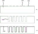
Fig. 7 schematically depicts an alternative embodiment of an ultrasound transducer arrangement 100 that may be folded into a rigid ultrasound transducer assembly 600 having a plurality of serpentine folds as schematically shown in fig. 8. In this embodiment, the flexible polymer assembly 150 is shaped as an elongated strip, wherein the ultrasound transducer arrangement 100 comprises, in addition to the ultrasound transducer substrate islands or chips 110 and the contact substrate islands or chips 120, a plurality of supporting substrate islands or chips 140 interconnected by the flexible polymer assembly 150 as explained before.
Support substrate islands or chips 140 are spaced apart such that the exposed major surfaces of adjacent support substrate islands or chips 140 may contact each other when flexible polymeric component 150 is folded into multiple serpentine loops or folds, wherein adjacent support substrate islands or chips 140 occupy a single fold or loop as shown in fig. 8. Adjacent support substrate islands or chips 140 may be secured to one another in any suitable manner (e.g., using a suitable adhesive). The supporting substrate island or chip 140 acts as a rigid support member for the ultrasound transducer assembly 600, which helps to impart its desired rigidity to the ultrasound transducer assembly 600.
In an embodiment, at least some of the supporting substrate islands or chips 140 may perform the previously described functions of mounting the substrate islands or chips 130. In other words, at least some of the support substrate islands or chips 140 may include contacts on exposed surfaces on which active components 132 (e.g., transducer controllers and/or signal processing components such as ICs, e.g., application specific ICs (asics)) or passive components 134 (e.g., decoupling capacitors or the like) may be mounted in any suitable manner (e.g., soldering, thermocompression bonding, etc.).
In an embodiment, the ultrasound transducer substrate island or chip 110 is spatially separated from another substrate island (e.g., one of the supporting substrate islands or chips 140) by a backing member 610, which may be a backing member as previously explained. The ultrasound transducer substrate islands or chips 110 and the further substrate islands may be secured to the backing member 610 in any suitable manner, for example using an adhesive.
The ultrasound transducer substrate island or chip 110 may be located at a proximal end of the ribbon-shaped flexible polymer assembly 150 and the contact substrate island or chip 120 may be located at a distal end of the ribbon-shaped flexible polymer assembly 150 relative to the backing member 610. As shown in fig. 8, the contact substrate island or chip 120 may be connected to a coaxial wire assembly 200 comprising a plurality of coaxial wires 220 as previously explained.
In fig. 9, a non-limiting example of a method according to an embodiment of the invention is schematically depicted, wherein an ultrasound transducer arrangement 100 is formed. In a first step, depicted in fig. 9(a), a wafer 900 is provided, wherein a plurality of ultrasound transducer substrate islands or chips 110 having a plurality of ultrasound transducer elements 112 and a plurality of first contacts 114 have been formed in one or more arrays 920, and wherein contact substrate islands or chips 120 comprising a plurality of second contacts 122 are formed in one or more arrays 930 (two arrays 920, 930 are shown by way of non-limiting example). The array 920 of ultrasound transducer substrate islands or chips 110 is separated from an adjacent array 930 of contact substrate islands or chips 120 by sacrificial regions 910 of wafer 900. The individual substrate islands or chips within each of the arrays 920, 930 are separated by additional sacrificial wafer regions 912 (e.g., scribe lines, etc., which will be explained in more detail later).
The method proceeds as shown in fig. 9(b), providing a layer of flexible electrically insulating material 150 on the front side of the wafer 900, which is subsequently patterned by photolithography to expose the first and second contacts 114, 122 underlying the layer 200. Any suitable material may be used for layer 200. The flexible electrically insulating material may be selected from the group consisting of parylene, polyimide resin, polycarbonate, fluorocarbon, polysulfone, epoxy, phenol, melamine, polyester, and silicone resin or copolymers thereof. Polyimide and parylene are particularly suitable when the IC is to be integrated into an invasive medical arrangement, as these materials have been specifically used for invasive medical devices.
The layer thickness of the flexible electrically insulating material 150 is preferably selected in the range of 1-20 μm and more preferably in the range of 1-10 μm to ensure sufficient flexibility of the result. If the layer 150 becomes too thick, its flexibility will decrease. However, if layer 150 becomes too thin, it may be too easily damaged.
In a subsequent step, shown in fig. 9(c), an electrically conductive material is deposited on the layer of flexible electrically insulating material 150 and subsequently patterned to provide respective electrically conductive traces 152 in electrically conductive contact with the exposed first and second contacts 114, 122 underlying the layer 150. Any suitable conductive material may also be used, such as Al, Cu, or other suitable metals and metal alloys.
In an optional step shown in fig. 9(d), the conductive traces 152 are then covered with a second layer of flexible, electrically insulating material 150', the second layer of flexible, electrically insulating material 150' preferably being the same material as used for layer 150, although this is not necessary. In other words, the materials for layers 150 and 150', respectively, may be individually selected from the group of suitable compounds described previously.
In a preferred embodiment, layers 150 and 150' are made of the same material (e.g., polyimide or parylene) and have the same thickness, e.g., about 5 μm. By using the same thickness for both layers 150 and 150', the conductive trace(s) 152 are located at the so-called neutral line of stress of the flexible contact extensions of the contacts 114, 122. The second layer 150' of flexible electrically insulating material, if present, may be covered with a thin protective layer (not shown) from a subsequent wafer processing step. Any suitable material may be used, for example a metal, such as Al. The use of a material that can serve both the protective layer 150 'during subsequent processing steps and a hard etch mask for subsequent patterning of the second layer of flexible electrically insulating material 150' is preferred because it reduces wafer processing complexity. For this reason, metals such as aluminum are preferred.
As shown in fig. 9(e), the method proceeds by applying and patterning a resist layer 902 on the backside of the wafer 900. Alternatively, the resist layer 902 may be replaced by a patterned hard mask. The patterned resist layer 902 may be any suitable material including similar or identical materials used for the aforementioned thin protective layer over the second layer 150', which protects (covers) the regions of the arrays 920, 930 in the wafer 500.
In a final step as shown in fig. 9(f), the exposed portions of the backside of the wafer 900 (i.e., the portions not covered by the patterned resist 902) are exposed to an etch recipe, preferably an anisotropic etch recipe such as a Bosch process, for example in the case where the wafer 900 is a silicon wafer, wherein the exposed portions are etched to a depth corresponding to the desired final thickness of the substrate islands or chips 110, 120 to be formed from the wafer 900, to release (singulate) arrays 920, 930, wherein each array 920 is connected to the array 530 by a flexible interconnect 200. It is noted that the Bosch process, which typically comprises successive etching and passivation steps, is known per se and will therefore not be described in further detail for the sake of brevity only. Of course other suitable etch recipes are also contemplated. The patterned resist 902 is then stripped from the backside of the wafer 900.
Although not specifically shown, additional singulation steps may be employed to singulate the ultrasound transducer arrangement 100, such as by cutting the sacrificial region 912. Alternatively, the etching step shown in step (f) may comprise removing the sacrificial region 912 such that the ultrasound transducer arrangement 100 is individualized during a single step.
In this regard, it should be noted that the wafer 900 may of course include further substrate islands, such as mounting substrate islands 130 and/or virtual substrate islands 140, wherein these further substrate islands may be connected to the ultrasound transducer substrate islands or chips 110 and/or contact substrate islands or chips 120 as explained above for electrical connection between the contacts 114, 122, if necessary. These further substrate islands are not shown for reasons of clarity only.
It should also be noted that the contact substrate island or chip 120 also includes a plurality of external contacts to connect the contact substrate island or chip 120 to the coaxial wire assembly 200, as previously explained. Again, these external contacts may be formed in any suitable manner and are not shown for clarity reasons only. In an embodiment, solder bumps may be formed on these external contacts. These solder bumps may be formed on the external contacts at any suitable point in the manufacturing process described above, for example before or after singulation of the arrays 520, 530. The solder bumps may be formed on the contacts in any suitable manner, such as by using a laser process available from PacTech corporation of Nauen, germany.
As previously mentioned, the ultrasound transducer arrangement 100 may comprise passive components 134, such as one or more capacitors, e.g. decoupling capacitors. Such a decoupling capacitance is typically required if the ultrasound transducer arrangement 100 includes components that generate switching transients that are large enough to compromise the integrity of the power supply. An example of such a component is a signal processing IC such as an ASIC. This problem is particularly prevalent at the end of miniature probes, where the power supply line tends to have a relatively high impedance of uncertainty. In such a case, decoupling capacitors are used to decouple various components from the power supply line so that these components are shielded from power supply fluctuations. Such decoupling capacitors have a capacitance typically ranging from 1 to 100 nF. Furthermore, discrete capacitors may be included to establish AC connections between different circuit portions operating at different DC potentials, for example in the case of CMUT transducer arrays and ASICs. Such capacitors must be electrically floating, i.e. must be dielectrically insulated from the substrate and ground.
The size of such discrete capacitors makes the integration of miniaturized ultrasound probe tips prohibitive because such capacitors are too large. In an embodiment, this problem is solved by integrating trench capacitors into at least some of the substrate islands 110, 120, 130 such that the need to include discrete capacitors in the ultrasound transducer arrangement 100 is avoided.
Advantageously, the ultrasound transducer arrangement 100 comprises a plurality of substrate islands comprising at least a first substrate island 110 and a second substrate island 120, the first substrate island 110 comprising a plurality of ultrasound transducer cells 112, the second substrate island 120 comprising an array of external contacts for connecting the ultrasound sensor arrangement to the flexible tubular body, wherein the plurality of substrate islands optionally further comprises at least one mounting substrate island 130 for mounting one or more active and/or passive components thereon as explained before. In an embodiment, at least two of the substrate islands each comprise a trench capacitor, which has the advantage that the respective trench capacitors are truly electrically isolated from each other due to the fact that they are located in different substrates, such that these different substrates can operate at different potentials. Furthermore, the inclusion of trench capacitors avoids the need to include discrete capacitors in the ultrasound transducer arrangement 100, thereby also facilitating miniaturization of the ultrasound transducer arrangement 100 and the ultrasound probe tip formed by such an arrangement.
In the context of the present application, a trench capacitor is a capacitor formed by a plurality of trenches extending almost perpendicularly from a main surface of a substrate into the substrate. The trenches may have any suitable shape, such as a profile, for example the trenches may be square, rectangular, circular trenches, etc. The substrate is typically a conductive or semiconductive substrate and serves as the first plate of the trench capacitor. These trenches are typically lined with an electrical insulator, such as a dielectric material, and filled with additional conductive or semiconductive material to serve as the second plate of the trench capacitor, wherein the electrical insulator separates the first plate from the second plate. Due to the fact that the plates of the trench capacitor extend in all three dimensions and are formed by a plurality of trenches, a capacitor is obtained which has a large plate area in a compact substrate volume, thereby enabling a compact high capacity capacitor.
Fig. 10 schematically depicts an exemplary embodiment of a method of manufacturing such a trench capacitor. It should be understood that alternative manufacturing methods are readily available and will be known to those skilled in the art. Such alternative manufacturing methods are also contemplated.
The method starts in step (a) with providing a conductive substrate 1000, which may be part of the wafer 900 and which may be converted into one of the above-described substrate islands 110, 120, 130 as previously explained, for example, with the aid of fig. 9. For example, the conductive substrate 1000 may be a highly conductive silicon substrate, such As an n-type substrate, e.g., an As-doped substrate, although a p-type substrate may also be used. Additionally, as previously explained, substrate materials other than silicon are also contemplated. A suitable etch mask 1002 is formed on the substrate 100, for example by growing a thermal oxide on the substrate 1000, which is opened where the trench of the trench capacitor is to be formed to create an opening 1004. Etch mask 1002 may be formed to any suitable thickness, for example, about 1 μm.
Next, as shown in step (b), the trench 1006 is etched using a suitable etch recipe (e.g., using deep reactive ion etching in the case of a silicon substrate 1000). The trench 1006 may be etched to a depth of about 50-60% of the final thickness of the substrate island to be formed. For example, for a substrate island having a final thickness of about 50 μm, the trench 1006 may be etched to a depth of about 30 μm. The trench 1006 may have any suitable width, such as a width of about 1-2 μm.
After etching of the hole 1006, a capacitor dielectric 1008 is deposited in step (c). Any suitable dielectric material may be used for this purpose. A particularly suitable material is silicon nitride, which may be deposited using LPCVD, for example. However, other dielectric materials, such as silicon oxide, aluminum oxide, or combinations of these materials, may also be used, and other deposition techniques, such as ALD, are also contemplated. The capacitor dielectric 1008 may be formed to any suitable thickness, such as a few tens of nm, such as 20 nm.
In step (d), the trench 1006 lined with the capacitor dielectric 1008 is filled with a conductive material 1010 to form a second plate of the trench capacitor. In an embodiment, the trench 1006 may be filled by depositing a layer of in-situ doped polysilicon, although other conductive materials may also be used. After patterning the conductive material 1010 (e.g., using a suitable etch recipe in step (e)), an additional dielectric layer 1012 is formed over the patterned conductive material 1010 in step (f) to electrically isolate the conductive material 1010 from subsequent metallization steps. Fabrication of the trench capacitor is completed by etching contact windows 1014, 1016 in step (g) and depositing and patterning a metal interconnect layer, such as an aluminum interconnect layer, in step (h) to form metal contacts 1020 and 1022 for the first and second plates of the trench capacitor, respectively. Since such finishing steps are known per se, they are not explained in further detail merely for the sake of brevity.
The substrate 1000 may then undergo further processing steps, for example to form an array of transducer elements thereon, as will be appreciated by those skilled in the art. For example, a passivation layer or layer stack may be formed on the trench capacitor, after which an array of ultrasound transducer elements (e.g. CMUT elements) may be formed on the passivation layer (stack), as is known per se. Other further processing steps, such as forming other elements on such substrates, will be apparent to those skilled in the art. It should also be understood that each substrate island may include a plurality of such trench capacitors.
Referring to fig. 11, an exemplary embodiment of an ultrasonic diagnostic imaging system with an array transducer probe according to an embodiment of the present invention is shown in block diagram form. In fig. 11, a CMUT transducer array 110 (not shown in fig. 11) on an ultrasound transducer chip 100 is provided on an ultrasound probe 10 to transmit an ultrasound wave and receive echo information. Transducer array 110 may alternatively include piezoelectric transducer elements formed from materials such as lead zirconate titanate (PZT) or polyvinylidene fluoride (PVDF). The transducer array 110 may be an array of one-or two-dimensional transducer elements that can be scanned in a two-dimensional plane or in three-dimensional space for 3D imaging.
The transducer array 110 is coupled to a microbeamformer 12 in the probe 10, the microbeamformer 12 controlling the transmission and reception of signals by CMUT array cells or piezoelectric elements. The microbeamformer is capable of at least partial beamforming of signals received by groups or "patches" of transducer elements, for example, as described in U.S. patents US 5997479(Savord et al), US6013032(Savord), and US 6623432(Powers et al).
The microbeamformer 12 is coupled to a transmit/receive (T/R) switch 16 by a probe cable (e.g., coaxial cable 410), the T/R switch 16 switches between transmit and receive and protects the main beamformer 20 from high energy transmit signals when the microbeamformer is not present or used, and the transducer array 110 is operated directly by the main system beamformer 20. The transmission of ultrasound beams from the transducer array 110 under the control of the microbeamformer 12 is directed by a transducer controller 18 coupled to the microbeamformer through a T/R switch 16 and a main system beamformer 20, which receives input from user operation of a user interface or control panel 38. One of the functions controlled by the transducer controller 18 is the direction in which the beam is steered and focused. The beams may be steered directly in front of the transducer array 110 (orthogonal to the transducer array 110) or at different angles for a wider field of view. The transducer controller 18 may be coupled to control a DC bias control 45 for the CMUT array. For example, the DC bias control 45 sets the DC bias voltage(s) applied to the CMUT cell(s) 150 of the CMUT array 110.
The partially beamformed signals produced by the microbeamformer 12 are forwarded to a main beamformer 20 where the partially beamformed signals from the individual patches of transducer elements are combined into a fully beamformed signal. For example, the main beamformer 20 may have 128 channels, where each channel receives partially beamformed signals from tens or hundreds of patches (see fig. 1-3) or piezoelectric elements of CMUT transducer cells 112. In this manner, signals received by the thousands of transducer elements of the transducer array 110 may effectively contribute to a single beamformed signal.
The beamformed signals are coupled to a signal processor 22. The signal processor 22 may process the echo signals in various ways, such as bandpass filtering, decimation, I and Q component separation, and harmonic signal separation, which acts to separate linear and nonlinear signals, thereby enabling the identification of nonlinear (higher harmonics of the fundamental frequency) echo signals returned from tissue and microbubbles.
The signal processor 22 optionally may perform additional signal enhancement such as speckle reduction, signal compounding, and noise cancellation. The band pass filter in the signal processor 22 may be a tracking filter whose pass band slides from a higher frequency band to a lower frequency band as echo signals are received from increasing depths, thereby suppressing noise at higher frequencies from greater depths where these frequencies lack anatomical information.
The processed signals are coupled to a B-mode processor 26 and optionally to a doppler processor 28. The B-mode processor 26 employs detection of the amplitude of the received ultrasound signals to image structures in the body, such as tissues of organs and blood vessels in the body. As described in US 6283919(Roundhill et al) and US 6458083(Jago et al), B-mode images of structures of the body can be formed in harmonic image modes or fundamental image modes or a combination of both.
A doppler processor 28, if present, processes temporally different signals from tissue motion and blood flow in order to detect motion of a substance, such as the flow of blood cells in an image field. The doppler processor typically includes a wall filter having parameters that can be set to pass and/or reject echoes returned from selected types of materials in the body. For example, a wall filter may be configured to have a passband characteristic that passes relatively low amplitude signals from higher velocity materials while rejecting relatively strong signals from lower or zero velocity materials.
This band pass characteristic will pass signals from flowing blood while rejecting signals from nearby stationary or slowly moving objects, such as the heart wall. The inverse nature will pass signals from moving tissue of the heart while rejecting blood flow signals, which is known as so-called tissue doppler imaging, which detects and depicts the motion of tissue. The doppler processor receives and processes a sequence of time-discrete echo signals from different points in the image field, the sequence of echoes from a particular point being referred to as an ensemble (ensemble). An ensemble of echoes received in rapid succession over a relatively short time interval may be used to estimate the doppler shift frequency of flowing blood, where the correspondence of doppler frequency to velocity is indicative of blood flow velocity. The ensemble of echoes received over a longer period of time is used to estimate the velocity of slower flowing blood or slowly moving tissue.
The structural and motion signals produced by the B-mode processor(s) (and doppler processor (s)) are coupled to the scan converter 32 and the multiplanar reformatter 44. The scan converter 32 arranges the echo signals in a spatial relationship according to which the echo signals are received in a desired image format. For example, the scan converter may arrange the echo signals into a two-dimensional (2D) fan format or a pyramidal three-dimensional (3D) image.
Implementing a scan converter may overlay the B-mode structure image with its doppler estimated velocity using colors corresponding to motion at points in the image field to produce a color doppler image depicting motion of tissue and blood flow in the image field. The multiplanar reformatter 44 converts echoes received from points in a common plane in a volumetric region of the body into an ultrasound image of that plane, for example as described in US patent US 6443896 (Detmer). The volume renderer 42 converts the echo signals of the 3D data set into a projected 3D image as seen from a given reference point, as described in US6530885(Entrekin et al).
The 2D or 3D image is coupled from the scan converter 32, the multi-plane reformatter 44 and the volume renderer 42 to the image processor 30 for further enhancement, buffering and temporary storage for display on the image display 40. In addition to being used for imaging, the blood flow values produced by the Doppler processor 28 and the tissue structure information produced by the B-mode processor 26 are coupled to a quantification processor 34. The quantification processor produces a measure of the different flow conditions (e.g., volumetric flow of blood flow) as well as structural measurements (e.g., size and gestational age of the organ). The quantification processor may receive input from the user control panel 38, such as points in the anatomy of the image in which measurements are to be made.
The output data from the quantization processor is coupled to a graphics processor 36 for rendering the measurement pattern and values using an image on a display 40. The graphics processor 36 may also generate a graphic overlay for display with the ultrasound images. These graphic overlays may contain standard identifying information (e.g., patient name, date and time of the image, imaging parameters, etc.). For these purposes, the graphics processor receives input from the user interface 38, such as a patient name.
The user interface is also coupled to the transmit controller 18 to control the generation of ultrasound signals from the transducer array 110 and, thus, the images produced by the transducer array and ultrasound system. The user interface is further coupled to a multiplanar reformatter 44 for selecting and controlling planes of a plurality of multiplanar reformatted (MPR) images that may be used to perform quantitative measurements in the image field of the MPR image.
As understood by those skilled in the art, the above embodiments of the ultrasonic diagnostic imaging system are intended to give a non-limiting example of such an ultrasonic diagnostic imaging system. One of ordinary skill in the art will immediately recognize that several variations of the architecture of an ultrasonic diagnostic imaging system are possible without departing from the teachings of the present invention. For example, as also noted in the above embodiments, the microbeamformer 12 and/or the doppler processor 28 can be omitted, the ultrasound probe 10 can have no three-dimensional imaging capability, or the like. Other variations will be apparent to those skilled in the art.
It should be noted that the above-mentioned embodiments illustrate rather than limit the invention, and that those skilled in the art will be able to design many alternative embodiments without departing from the scope of the appended claims. In the claims, any reference signs placed between parentheses shall not be construed as limiting the claim. The word "comprising" does not exclude the presence of other elements or steps than those listed in a claim. The word "a" or "an" preceding an element does not exclude the presence of a plurality of such elements. The invention can be implemented by means of hardware comprising several distinct elements. In the device claim enumerating several means, several of these means may be embodied by one and the same item of hardware. The mere fact that certain measures are recited in mutually different dependent claims does not indicate that a combination of these measures cannot be used to advantage.
Claims (14)
1. An ultrasonic transducer assembly (600) comprising:
a foldable ultrasound transducer arrangement (100) comprising a plurality of substrate islands (110, 120, 130) spatially separated and electrically interconnected by a flexible polymer component (150), the flexible polymer component comprising electrically conductive traces providing the electrical interconnections, the plurality of substrate islands comprising a first substrate island (110) comprising a plurality of ultrasound transducer cells (112) and a second substrate island (120) comprising an array of external contacts for connecting the foldable ultrasound transducer arrangement to a flexible tubular body; and
a rigid support structure (400) having a first planar portion (410) including a first surface, a second planar portion (420) opposite the first planar portion, the second planar portion having a second surface, and a third planar portion (430) having a third surface extending between the first and second surfaces;
wherein the foldable ultrasound transducer arrangement is arranged to be folded onto the rigid support structure such that the first substrate island (110) is mounted on the first surface and a second substrate island (120) is mounted on the second surface.
2. The ultrasound transducer assembly (600) of claim 1, wherein the foldable ultrasound transducer arrangement (100) further comprises at least one further substrate island (130) comprising a plurality of external contacts for receiving active and/or passive components (132, 134), the at least one further substrate island being mounted on the third planar portion (430).
3. The ultrasound transducer assembly (600) of claim 2, further comprising active and/or passive components (132, 134) mounted on the at least one further substrate island (130).
4. The ultrasonic transducer assembly (600) of claim 2, wherein at least one of said first substrate island (110), said second substrate island (120) and said at least one further substrate island (130) comprises a plurality of trenches (1006) defining decoupling capacitors, each trench being filled with a conductive material (1010), said conductive material being separated from a substrate material (1000) by an electrically insulating material (1008).
5. The ultrasound transducer assembly (600) of claim 4, comprising a plurality of said decoupling capacitors, each decoupling capacitor being positioned on a different substrate island (110, 120, 130).
6. The ultrasound transducer assembly (600) of claim 1, wherein the rigid support structure (400) is a metal support structure.
7. The ultrasonic transducer assembly (600) according to any one of claims 1-6, wherein said first substrate island (110) is separated from said first surface by a backing member (610).
8. The ultrasonic transducer assembly (600) according to claim 7, wherein at least a portion of said flexible polymer assembly (150) extends along an outer surface of said backing member.
9. A coaxial wire assembly (200), comprising:
a plurality of coaxial wires (220), each having a conductive core (228) covered by an electrically insulating sleeve (226); and
an electrical insulator (210) having a first major surface (211), a second major surface (213), and a plurality of through holes (212), each of the plurality of through holes extending from the first major surface to the second major surface, each of the holes being coated with an electrically conductive member;
wherein each coaxial wire includes an exposed terminal core portion mounted in one of the plurality of through holes from the first major surface, and wherein each through hole is sealed by a solder bump (214) on the second major surface.
10. The coaxial wire assembly (200) of claim 9, further comprising a flexible tubular body housing the coaxial wire (220), wherein the electrical insulator (210) is mounted on an end portion of the flexible tubular body.
11. An ultrasound probe comprising the ultrasound transducer assembly (600) of any of claims 1 to 8.
12. An ultrasound probe comprising the ultrasound transducer assembly (600) of any of claims 1 to 7, wherein a total length from the first substrate island (110) to the second substrate island (120) is less than 10mm or less than 8 mm.
13. An ultrasound probe comprising the ultrasound transducer assembly (600) of any of claims 1-8 and the coaxial wire assembly (200) of claim 9, wherein each of the external contacts of the second substrate island (120) is electrically coupled to one of the solder bumps (214).
14. An ultrasound imaging system (1) comprising an ultrasound probe according to any of claims 11 to 13.
Applications Claiming Priority (3)
| Application Number | Priority Date | Filing Date | Title |
|---|---|---|---|
| EP14177454.7 | 2014-07-17 | ||
| EP14177454 | 2014-07-17 | ||
| PCT/EP2015/064365 WO2016008690A1 (en) | 2014-07-17 | 2015-06-25 | Ultrasound transducer arrangement and assembly, coaxial wire assembly, ultrasound probe and ultrasonic imaging system |
Publications (2)
| Publication Number | Publication Date |
|---|---|
| CN106536068A CN106536068A (en) | 2017-03-22 |
| CN106536068B true CN106536068B (en) | 2020-06-05 |
Family
ID=51211086
Family Applications (1)
| Application Number | Title | Priority Date | Filing Date |
|---|---|---|---|
| CN201580039047.1A Active CN106536068B (en) | 2014-07-17 | 2015-06-25 | Ultrasound transducer arrangement and assembly, coaxial wire assembly, ultrasound probe and ultrasound imaging system |
Country Status (5)
| Country | Link |
|---|---|
| US (2) | US10828673B2 (en) |
| EP (2) | EP3169448A1 (en) |
| JP (3) | JP6670292B2 (en) |
| CN (1) | CN106536068B (en) |
| WO (1) | WO2016008690A1 (en) |
Families Citing this family (21)
| Publication number | Priority date | Publication date | Assignee | Title |
|---|---|---|---|---|
| US11325828B2 (en) * | 2013-02-22 | 2022-05-10 | Vibrant Composites Inc. | High-volume millimeter scale manufacturing |
| EP3140049B1 (en) * | 2014-05-06 | 2018-08-01 | Koninklijke Philips N.V. | Ultrasonic transducer chip assembly, ultrasound probe, ultrasonic imaging system and ultrasound assembly and probe manufacturing methods |
| EP3169448A1 (en) * | 2014-07-17 | 2017-05-24 | Koninklijke Philips N.V. | Ultrasound transducer arrangement and assembly, coaxial wire assembly, ultrasound probe and ultrasonic imaging system |
| US20170055948A1 (en) * | 2015-08-27 | 2017-03-02 | Tyco Electronics Corporation | Probe assembly and system including a modular device and a cable assembly |
| WO2017182344A1 (en) * | 2016-04-19 | 2017-10-26 | Koninklijke Philips N.V. | Ultrasound transducer positioning |
| EP3518776B1 (en) * | 2016-09-29 | 2020-11-25 | Koninklijke Philips N.V. | Guide member for electrical cable alignment and attachment and associated intraluminal devices |
| US11963823B2 (en) | 2016-10-03 | 2024-04-23 | Koninklijke Philips N.V. | Radiopaque arrangement of electronic components in intra-cardiac echocardiography (ICE) catheter |
| US10088642B2 (en) | 2016-11-09 | 2018-10-02 | International Business Machines Corporation | Coaxial wire and optical fiber trace via hybrid structures and methods to manufacture |
| GB2555835B (en) * | 2016-11-11 | 2018-11-28 | Novosound Ltd | Ultrasound transducer |
| WO2018132443A1 (en) * | 2017-01-10 | 2018-07-19 | The Regents Of The University Of California | Stretchable ultrasonic transducer devices |
| EP3369383A1 (en) * | 2017-03-02 | 2018-09-05 | Koninklijke Philips N.V. | Ultrasound device |
| EP3619727A4 (en) * | 2017-05-02 | 2021-02-17 | L. Pierre De Rochemont | High speed semiconductor chip stack |
| JP7145892B2 (en) | 2017-06-30 | 2022-10-03 | コーニンクレッカ フィリップス エヌ ヴェ | Intracavitary ultrasound imaging device having a substrate separated into a plurality of spaced apart segments, intracavitary ultrasound imaging device with grooves, and method of manufacture |
| US11642099B2 (en) * | 2017-12-08 | 2023-05-09 | Koninklijke Philips N.V. | Rolled flexible substrate with integrated window for intraluminal ultrasound |
| CN112004480A (en) * | 2018-02-09 | 2020-11-27 | 皇家飞利浦有限公司 | Flexible support members for intraluminal imaging devices and associated devices, systems, and methods |
| CN109031259A (en) * | 2018-07-24 | 2018-12-18 | 常州波速传感器有限公司 | Ultrasonic probe |
| CN111447533B (en) * | 2019-01-16 | 2021-05-18 | 昆山康龙电子科技有限公司 | Internal module formed by metal material belt |
| EP4003612B1 (en) | 2019-07-24 | 2024-05-15 | Vermon S.A. | Method of manufacturing a panel transducer scale package |
| US11959707B2 (en) * | 2019-10-10 | 2024-04-16 | Sunnybrook Research Institute | Systems and methods for cooling ultrasound transducers and ultrasound transducer arrays |
| US11207140B2 (en) * | 2019-12-18 | 2021-12-28 | GE Precision Healthcare LLC | Ultrasound-enabled invasive medical device and method of manufacturing an ultrasound-enabled invasive medical device |
| CN117257351B (en) * | 2023-11-22 | 2024-04-23 | 深圳欢影医疗科技有限公司 | High-performance micro linear array transducer and preparation method thereof |
Citations (5)
| Publication number | Priority date | Publication date | Assignee | Title |
|---|---|---|---|---|
| EP0853919A2 (en) * | 1997-01-08 | 1998-07-22 | Endosonics Corporation | A high resolution intravascular ultrasound transducer assembly having a flexible substrate and method for manufacture thereof |
| CN1930689A (en) * | 2004-03-10 | 2007-03-14 | 皇家飞利浦电子股份有限公司 | Trench-gate transistors and their manufacture |
| CN201270345Y (en) * | 2008-09-12 | 2009-07-08 | 镇江天安电信电器有限公司(中外合资) | Insulator for coaxial cable connector |
| CN101868185A (en) * | 2007-12-03 | 2010-10-20 | 科隆科技公司 | CMUT packaging for ultrasound system |
| CN101960673A (en) * | 2008-03-14 | 2011-01-26 | 胡贝尔和茹纳股份公司 | Multiple coaxial cable plug connection and method for installing such a multiple coaxial cable plug connection |
Family Cites Families (24)
| Publication number | Priority date | Publication date | Assignee | Title |
|---|---|---|---|---|
| JPH04179074A (en) | 1990-11-13 | 1992-06-25 | Toshiba Corp | Method for connecting multi-core cable |
| DE69516444T2 (en) * | 1994-03-11 | 2001-01-04 | Intravascular Res Ltd | Ultrasonic transducer arrangement and method for its production |
| US6283919B1 (en) | 1996-11-26 | 2001-09-04 | Atl Ultrasound | Ultrasonic diagnostic imaging with blended tissue harmonic signals |
| US6458083B1 (en) | 1996-11-26 | 2002-10-01 | Koninklijke Philips Electronics N.V. | Ultrasonic harmonic imaging with adaptive image formation |
| US5947905A (en) * | 1997-10-15 | 1999-09-07 | Advanced Coronary Intervention, Inc. | Ultrasound transducer array probe for intraluminal imaging catheter |
| US6013032A (en) | 1998-03-13 | 2000-01-11 | Hewlett-Packard Company | Beamforming methods and apparatus for three-dimensional ultrasound imaging using two-dimensional transducer array |
| US5997479A (en) | 1998-05-28 | 1999-12-07 | Hewlett-Packard Company | Phased array acoustic systems with intra-group processors |
| JP2001178724A (en) * | 1999-12-22 | 2001-07-03 | Olympus Optical Co Ltd | Ultrasonic probe |
| US6530885B1 (en) | 2000-03-17 | 2003-03-11 | Atl Ultrasound, Inc. | Spatially compounded three dimensional ultrasonic images |
| US6443896B1 (en) | 2000-08-17 | 2002-09-03 | Koninklijke Philips Electronics N.V. | Method for creating multiplanar ultrasonic images of a three dimensional object |
| US6468216B1 (en) | 2000-08-24 | 2002-10-22 | Kininklijke Philips Electronics N.V. | Ultrasonic diagnostic imaging of the coronary arteries |
| JP2002352877A (en) * | 2001-05-29 | 2002-12-06 | Hitachi Cable Ltd | Terminal connection and connection method of minute coaxial cable |
| US20030236443A1 (en) | 2002-04-19 | 2003-12-25 | Cespedes Eduardo Ignacio | Methods and apparatus for the identification and stabilization of vulnerable plaque |
| JP4571435B2 (en) * | 2004-05-27 | 2010-10-27 | ジーイー・メディカル・システムズ・グローバル・テクノロジー・カンパニー・エルエルシー | Ultrasonic probe |
| JP4575372B2 (en) * | 2004-06-10 | 2010-11-04 | オリンパス株式会社 | Capacitive ultrasonic probe device |
| EP1949419A1 (en) * | 2005-11-08 | 2008-07-30 | Nxp B.V. | Trench capacitor device suitable for decoupling applications in high-frequency operation |
| JP5069745B2 (en) * | 2006-06-20 | 2012-11-07 | エヌエックスピー ビー ヴィ | Integrated circuit and assembly comprising the same |
| US8403858B2 (en) * | 2006-10-12 | 2013-03-26 | Perceptive Navigation Llc | Image guided catheters and methods of use |
| JP5261929B2 (en) | 2006-12-15 | 2013-08-14 | 株式会社デンソー | Semiconductor device |
| CN101270345A (en) | 2008-02-13 | 2008-09-24 | 南开大学 | 1-strain pseudomonas mendocina and uses thereof |
| IN2013CN03726A (en) * | 2010-11-18 | 2015-08-07 | Koninkl Philips Electronics Nv | |
| EP2846699A4 (en) * | 2012-05-11 | 2016-01-27 | Volcano Corp | Circuit architectures and electrical interfaces for rotational intravascular ultrasound (ivus) devices |
| EP3169448A1 (en) * | 2014-07-17 | 2017-05-24 | Koninklijke Philips N.V. | Ultrasound transducer arrangement and assembly, coaxial wire assembly, ultrasound probe and ultrasonic imaging system |
| US10192281B2 (en) | 2016-07-07 | 2019-01-29 | Intel Corporation | Graphics command parsing mechanism |
-
2015
- 2015-06-25 EP EP15731346.1A patent/EP3169448A1/en not_active Withdrawn
- 2015-06-25 US US15/326,055 patent/US10828673B2/en active Active
- 2015-06-25 CN CN201580039047.1A patent/CN106536068B/en active Active
- 2015-06-25 EP EP20200436.2A patent/EP3795262A1/en not_active Withdrawn
- 2015-06-25 JP JP2017501646A patent/JP6670292B2/en active Active
- 2015-06-25 WO PCT/EP2015/064365 patent/WO2016008690A1/en active Application Filing
-
2019
- 2019-10-17 JP JP2019190035A patent/JP6878546B2/en active Active
-
2020
- 2020-10-20 US US17/075,179 patent/US20210031234A1/en active Pending
-
2021
- 2021-04-28 JP JP2021075645A patent/JP2021129996A/en active Pending
Patent Citations (5)
| Publication number | Priority date | Publication date | Assignee | Title |
|---|---|---|---|---|
| EP0853919A2 (en) * | 1997-01-08 | 1998-07-22 | Endosonics Corporation | A high resolution intravascular ultrasound transducer assembly having a flexible substrate and method for manufacture thereof |
| CN1930689A (en) * | 2004-03-10 | 2007-03-14 | 皇家飞利浦电子股份有限公司 | Trench-gate transistors and their manufacture |
| CN101868185A (en) * | 2007-12-03 | 2010-10-20 | 科隆科技公司 | CMUT packaging for ultrasound system |
| CN101960673A (en) * | 2008-03-14 | 2011-01-26 | 胡贝尔和茹纳股份公司 | Multiple coaxial cable plug connection and method for installing such a multiple coaxial cable plug connection |
| CN201270345Y (en) * | 2008-09-12 | 2009-07-08 | 镇江天安电信电器有限公司(中外合资) | Insulator for coaxial cable connector |
Also Published As
| Publication number | Publication date |
|---|---|
| JP2017528178A (en) | 2017-09-28 |
| JP2020032199A (en) | 2020-03-05 |
| US20170209898A1 (en) | 2017-07-27 |
| JP6670292B2 (en) | 2020-03-18 |
| US10828673B2 (en) | 2020-11-10 |
| US20210031234A1 (en) | 2021-02-04 |
| EP3795262A1 (en) | 2021-03-24 |
| WO2016008690A1 (en) | 2016-01-21 |
| CN106536068A (en) | 2017-03-22 |
| EP3169448A1 (en) | 2017-05-24 |
| JP2021129996A (en) | 2021-09-09 |
| JP6878546B2 (en) | 2021-05-26 |
Similar Documents
| Publication | Publication Date | Title |
|---|---|---|
| CN106536068B (en) | Ultrasound transducer arrangement and assembly, coaxial wire assembly, ultrasound probe and ultrasound imaging system | |
| US11931777B2 (en) | Ultrasonic transducer chip assembly, ultrasound probe, ultrasonic imaging system and ultrasound assembly and probe manufacturing methods | |
| JP7227318B2 (en) | IC dies, probes, and ultrasonic systems | |
| Dausch et al. | In vivo real-time 3-D intracardiac echo using PMUT arrays | |
| JP6482558B2 (en) | Monolithically integrated three-electrode CMUT device | |
| CN108348217B (en) | Ultrasound transducer array, probe and system | |
| US10586753B2 (en) | IC die, ultrasound probe, ultrasonic diagnostic system and method | |
| JP6767474B2 (en) | Capacitive Micromachine Ultrasonic Transducer with Increased Life | |
| WO2005114820A2 (en) | Implantable ultrasonic transducer systems and methods | |
| Chen et al. | A monolithic three-dimensional ultrasonic transducer array for medical imaging |
Legal Events
| Date | Code | Title | Description |
|---|---|---|---|
| C06 | Publication | ||
| PB01 | Publication | ||
| SE01 | Entry into force of request for substantive examination | ||
| SE01 | Entry into force of request for substantive examination | ||
| GR01 | Patent grant | ||
| GR01 | Patent grant |