CN106019917B - Electronic device and method for initializing control unit of electronic device - Google Patents
Electronic device and method for initializing control unit of electronic device Download PDFInfo
- Publication number
- CN106019917B CN106019917B CN201610097361.1A CN201610097361A CN106019917B CN 106019917 B CN106019917 B CN 106019917B CN 201610097361 A CN201610097361 A CN 201610097361A CN 106019917 B CN106019917 B CN 106019917B
- Authority
- CN
- China
- Prior art keywords
- voltage
- secondary battery
- threshold voltage
- electronic device
- initialization
- Prior art date
- Legal status (The legal status is an assumption and is not a legal conclusion. Google has not performed a legal analysis and makes no representation as to the accuracy of the status listed.)
- Active
Links
Images


Classifications
-
- G—PHYSICS
- G06—COMPUTING; CALCULATING OR COUNTING
- G06F—ELECTRIC DIGITAL DATA PROCESSING
- G06F1/00—Details not covered by groups G06F3/00 - G06F13/00 and G06F21/00
- G06F1/24—Resetting means
-
- G—PHYSICS
- G04—HOROLOGY
- G04G—ELECTRONIC TIME-PIECES
- G04G19/00—Electric power supply circuits specially adapted for use in electronic time-pieces
- G04G19/10—Arrangements for supplying back-up power
-
- G—PHYSICS
- G06—COMPUTING; CALCULATING OR COUNTING
- G06F—ELECTRIC DIGITAL DATA PROCESSING
- G06F1/00—Details not covered by groups G06F3/00 - G06F13/00 and G06F21/00
- G06F1/26—Power supply means, e.g. regulation thereof
- G06F1/263—Arrangements for using multiple switchable power supplies, e.g. battery and AC
-
- H—ELECTRICITY
- H03—ELECTRONIC CIRCUITRY
- H03K—PULSE TECHNIQUE
- H03K17/00—Electronic switching or gating, i.e. not by contact-making and –breaking
- H03K17/22—Modifications for ensuring a predetermined initial state when the supply voltage has been applied
-
- G—PHYSICS
- G04—HOROLOGY
- G04C—ELECTROMECHANICAL CLOCKS OR WATCHES
- G04C10/00—Arrangements of electric power supplies in time pieces
- G04C10/02—Arrangements of electric power supplies in time pieces the power supply being a radioactive or photovoltaic source
Abstract
The invention relates to an electronic device and an initialization method of a control unit of the electronic device. The electronic device includes a secondary battery and a control unit that receives power supply from the secondary battery and performs drive control of one or more other circuits driven by the secondary battery supplied with power, and is provided with an initialization unit that starts processing for outputting an initialization signal instructing initialization to the control unit at a predetermined timing when a voltage of the secondary battery decreases to a first threshold voltage or less higher than an operation guaranteed voltage set by the control unit and the state continues for a predetermined time, and stops output of the initialization signal when the voltage of the secondary battery increases to a second threshold voltage or more higher than the operation guaranteed voltage set by the control unit.
Description
Technical Field
The present invention relates to an electronic device using a secondary battery.
Background
Electronic devices using a secondary battery as a power source, such as an electronic timepiece (hereinafter, referred to as a "solar watch") having a solar cell, are widely used. When such an electronic apparatus is driven in a state where the electronic apparatus is placed in a dark place or the like without charging the secondary battery, the power supply voltage gradually decreases. In such an electronic device, when the power supply voltage is lower than a lower limit value of a voltage (hereinafter, referred to as an operation guarantee voltage) for guaranteeing a normal operation of a control Unit such as a CPU (Central Processing Unit), the control Unit may fail to perform a normal control and may be in a runaway state (a runaway state ). Even in the case where the charging of the power supply and the power consumption are performed simultaneously, if the state where the charging current is lower than the consumption current continues, it is possible to become the runaway state. Further, when the charging of the power source and the power consumption are performed simultaneously, there is a fear that: the power supply voltage surmounting action guarantee voltage fluctuates due to charging and power consumption, so that the generation of runaway and recovery from a runaway state occur repeatedly. Various techniques have been proposed to prevent such occurrence of runaway and repetition of recovery from a runaway state (hereinafter referred to as "continuation of a runaway state"), and the technique disclosed in patent document 1 is given as an example thereof. In the technique disclosed in patent document 1, when the power supply voltage is lower than a voltage set higher than the operation guarantee voltage (hereinafter, referred to as a set voltage), an initialization signal instructing initialization is periodically output to a CPU or the like to initialize the system, thereby preventing continuation of the runaway state.
Patent document 1: japanese patent laid-open publication No. 2006-153669
However, in the technique disclosed in patent document 1, there is a fear that: when the power supply voltage is lower than the set voltage due to a temporary voltage drop caused by a heavy load, an initialization signal is output, and the system is unintentionally initialized. For example, when the technique disclosed in patent document 1 is applied to a solar watch with an alarm (alarm), there are cases where: the system is initialized due to a temporary voltage drop caused by the alarm ringing.
Disclosure of Invention
The present invention has been made in view of the above problems, and an object thereof is to provide the following technology: in an electronic apparatus using a secondary battery, a situation where a system is inadvertently initialized due to a temporary voltage drop is avoided, and continuation of a runaway state is prevented.
In order to solve the above problem, the present invention provides an electronic device including: a secondary battery; a control unit that receives power supply from the secondary battery and performs drive control of one or more other circuits that are driven by the secondary battery; and an initialization unit that starts a process of outputting an initialization signal instructing initialization to the control unit at a predetermined timing when a voltage of the secondary battery decreases to a value equal to or lower than a first threshold voltage set higher than an operation guaranteed voltage of the control unit and the state continues for a predetermined time, and stops an output of the initialization signal when a voltage of the secondary battery increases to a value equal to or higher than a second threshold voltage set higher than the operation guaranteed voltage of the control unit.
According to such an electronic apparatus, even if the voltage of the secondary battery drops below the first threshold voltage due to the driving of any of the one or more other circuits, the initialization signal is not output as long as the time length during which the voltage of the secondary battery is lower than the first threshold voltage is shorter than the predetermined time. Therefore, even if the voltage of the secondary battery temporarily falls below the first threshold voltage due to the driving of any of the one or more other circuits, it is not inadvertently initialized. In the electronic apparatus according to the present invention, the process of outputting the initialization signal at the predetermined timing is continued until the voltage of the secondary battery rises to the second threshold voltage or more, and therefore, the runaway state can be prevented from continuing.
As another aspect of the present invention, it is considered to provide a method for initializing a control unit of an electronic device, the electronic device including: a secondary battery; one or more other circuits driven by power supplied from the secondary battery; and a control unit that receives power supply from the secondary battery and executes drive control of the one or more other circuits, wherein when a voltage of the secondary battery drops below a first threshold voltage set higher than an operation guaranteed voltage of the control unit and the state continues for a predetermined time, a process of transmitting an initialization signal instructing initialization to the control unit at a predetermined timing is started, and when a voltage of the secondary battery rises above a second threshold voltage set higher than the operation guaranteed voltage of the control unit, an output of the initialization signal is stopped. According to such an initialization method, it is possible to prevent the system from being initialized unintentionally due to a temporary voltage drop, and to prevent the runaway state from continuing.
In the present invention, the first threshold voltage is a threshold value in the case of a decrease in voltage for the secondary battery, and the second threshold voltage is a threshold value in the case of an increase in voltage for the secondary battery. Therefore, the second threshold voltage is preferably set to the same value as or a value larger than the first threshold voltage.
In a more preferred aspect, the control unit stops driving of a predetermined circuit of the one or more other circuits when the voltage of the secondary battery becomes lower than the first threshold voltage. According to this aspect, it is possible to reduce the power consumption since the voltage of the secondary battery becomes lower than the first threshold voltage, and to shorten the time until the secondary battery returns to the normal operation. In another preferred aspect, the control unit stops driving of a predetermined circuit among the one or more other circuits when the voltage of the secondary battery becomes lower than a third threshold voltage set higher than the first threshold voltage. According to this aspect, the time until the voltage of the secondary battery becomes lower than the first threshold voltage can be increased, and the normal operation state can be maintained for a long time.
In another preferred embodiment, a threshold voltage (fourth threshold voltage) at the start of operation of the electronic device or after system initialization is set, and the initialization unit may execute processing for outputting the initialization signal at a predetermined timing until the voltage of the secondary battery rises above the fourth threshold voltage at the start of operation of the electronic device or after system initialization. The fourth threshold voltage is set to be higher than the operation guaranteed voltage of the control means. The fourth threshold voltage may be a value different from any of the first and second threshold voltages, and may be a value equal to at least one of the first threshold voltage and the second threshold voltage. If the fourth threshold voltage is set to a value different from the second threshold voltage, it is possible to flexibly determine whether or not initialization of the control unit is necessary using different threshold voltages at the time of start of operation or at the time of voltage increase after system initialization and at the time of voltage increase thereafter.
In a more preferable aspect, the predetermined time is set shorter than a time during which the voltage of the secondary battery decreases from the first threshold voltage to the operation guaranteed voltage when the electronic device is operated in a state where power is not supplied to the secondary battery. Therefore, runaway of the control unit due to voltage drop of the secondary battery can be reliably prevented.
In a more preferred aspect, the electronic device further includes a monitoring timer that initializes a system when a predetermined time elapses, and the initializing unit resets the time counted by the monitoring timer at a predetermined timing when the voltage of the secondary battery is higher than the first threshold voltage, and suspends the resetting of the monitored time when a state in which the voltage of the secondary battery has dropped to the first threshold voltage or lower continues for the predetermined time or longer. In electronic devices such as electronic clocks, a watchdog timer is often provided to avoid software runaway. According to this aspect, in an electronic apparatus using a secondary battery using a monitoring timer provided in the electronic apparatus, it is possible to prevent the system from being unintentionally initialized due to a temporary voltage drop, and to prevent the runaway state from continuing.
In a more preferred aspect, the electronic device further includes a voltage generation unit and a switch interposed in parallel between a higher potential-side power supply line and a lower potential-side power supply line for supplying power to the one or more other circuits and the control unit, and a higher potential-side terminal of the secondary battery, wherein the initialization unit turns off the switch when an output of the initialization signal is started, turns on the switch when an output of the initialization signal is stopped, and compares a potential difference between the higher potential-side power supply line and the lower potential-side power supply line with the second threshold voltage as a voltage of the secondary battery. Examples of the voltage generating means include a diode and a resistor, and examples of the switch include a transistor switch. In such an embodiment, the potential difference between the high-potential-side power supply line and the low-potential-side power supply line is equal to the voltage of the high-potential-side terminal of the secondary battery in the on state of the switch, and is equal to the voltage obtained by adding the voltage generated by the voltage generation unit (the voltage of the voltage drop portion caused by the current flowing into the secondary battery via the diode or the like) to the voltage of the high-potential-side terminal of the secondary battery in the off state of the switch. That is, according to this aspect, the voltage of the comparison target to be compared with the second threshold voltage is boosted by the voltage generating means, and the time for returning to the normal operation can be shortened.
Drawings
Fig. 1 is a plan view showing an external appearance of an electronic timepiece 10A as a first embodiment of an electronic device of the present invention.
Fig. 2 is a perspective view showing the external appearance of the electronic timepiece 10A.
Fig. 3 is a sectional view showing a cross section of the electronic timepiece 10A.
Fig. 4 is a block diagram showing an example of the electrical configuration of the electronic timepiece 10A.
Fig. 5 is a timing chart showing the operation of the electronic timepiece 10A.
Fig. 6 is a timing chart showing the operation of the electronic timepiece 10A.
Fig. 7 is a block diagram showing an example of an electrical configuration of an electronic timepiece 10B as a second embodiment of the electronic apparatus of the present invention.
Fig. 8 is a timing chart showing the operation of the electronic timepiece 10B.
Fig. 9 is a flowchart showing a flow of operations executed by the CPU202 of the electronic timepiece 10B.
Fig. 10 is a diagram for explaining a modification (4).
Description of the reference symbols
10A, 10B: an electronic timepiece; 11: a dial plate; 15: a calendar small window; 21. 22, 23: a pointer; 25: a pointer shaft; 30: an outer case; 31: a housing; 32: a bezel; 33: a glass cover; 34: a back cover; 40: a dial ring; 50: a crown; 61: a button; 62: a button B; 63: a C button; 64: a D button; 70: a first small window; 71. 81, 91: a pointer; 80: a second small window; 90: a third small window; 92: indicia (electric quantity indicator); 120: a circuit substrate; 123: a circuit pressing plate; 125: a base plate; 130: a secondary battery; 135: a solar panel; 140: a drive mechanism; 150: a control display unit; 200: a ROM; 201: a RAM; 202: a CPU; 300: a clock signal generating circuit; 301: an oscillation circuit; 302: a frequency dividing circuit; 303: an oscillation stop detection circuit; 400: a peripheral circuit; 401: a stopwatch control circuit; 402: a timer control circuit; 403: a motor control circuit; 404: an input/output control circuit; 405: monitoring a timer; 500: initializing a circuit; 501: a first voltage detection circuit; 502: a timer; 503: a second voltage detection circuit; 504. 507: an OR gate; 505: an SR latch; 506: a reset circuit; 600: a charge control circuit; 700: an alarm sounding mechanism; 800: a fast start circuit; 801: a voltage generating unit; 802: and (4) switching.
Detailed Description
Next, embodiments of the present invention will be described with reference to the drawings.
(A: first embodiment)
(A-1: Structure)
Fig. 1 is a plan view showing an external appearance of an electronic timepiece 10A as a first embodiment of an electronic device according to the present invention, and fig. 2 is a perspective view showing the external appearance of the electronic timepiece 10A. The electronic timepiece 10A is a multifunction solar watch with an alarm having an alarm ringing function and a stopwatch function. As shown in fig. 1 to 3, the electronic timepiece 10A includes an outer case 30, a glass cover 33, and a back cover 34. The outer case 30 is configured such that a bezel 32 made of ceramic is fitted to a cylindrical case 31 made of metal. A disk-shaped dial 11 is disposed as a time display portion on the inner peripheral side of the bezel 32 via an annular dial ring 40 made of plastic.
The dial 11 has hands 21, 22, 23. Further, on the dial 11, from the center, a circular first small window 70 and a pointer 71 are provided in the 2-point direction, a circular second small window 80 and a pointer 81 are provided in the 10-point direction, a circular third small window 90 and a pointer 91 are provided in the 6-point direction, and a rectangular calendar small window 15 is provided in the 4-point direction. The dial 11, the hands 21, 22, 23, the first small window 70, the second small window 80, the third small window 90, the calendar small window 15, and the like can be visually confirmed through the glass cover 33.
On the outer periphery of the range from the 7-point direction to the 9-point direction of the third small window 90, crescent-shaped marks 92 are marked along the circumference, the base end in the 9-point direction being thick and the tip end in the 7-point direction being thin. The mark 92 is a charge indicator of the secondary battery 130 (see fig. 3), and the pointer 91 indicates any one of the base end, the distal end, and the middle according to the remaining amount of the battery.
On the side surface of the outer case 30, from the center of the dial 11, an a button 61 is provided at a position in the 8-point direction, a B button 62 is provided at a position in the 10-point direction, a C button 63 is provided at a position in the 2-point direction, a D button 64 is provided at a position in the 4-point direction, and the crown 50 is provided at a position in the 3-point direction. By operating these a button 61, B button 62, C button 63, D button 64, and crown 50, an operation signal corresponding to the operation is output.
As shown in fig. 3, in the electronic timepiece 10A, of two openings of the metal outer case 30, the opening on the front side is closed by a glass cover 33 via a bezel 32, and the opening on the rear side is closed by a back cover 34 made of metal. The outer case 30 includes the following components inside: a dial ring 40 attached to the inner periphery of the bezel 32, a translucent dial 11, a pointer shaft 25 penetrating the dial 11, pointers 21, 22, 23 rotating about the pointer shaft 25, and a drive mechanism 140 for driving the pointers 21, 22, 23. The pointer shaft 25 passes through the center of the outer case 30 in a plan view and is provided along a central axis extending in the front-back direction.
The dial 11 is a circular plate material that displays the time inside the outer case 30, and is formed of a translucent material such as plastic, and the dials 21, 22, 23 and the like are provided between the dial 11 and the glass cover 33, and the dial 11 is disposed inside the dial ring 40.
A solar panel 135 for performing photovoltaic power generation is provided between the dial 11 and the bottom plate 125 to which the driving mechanism 140 is attached. The solar panel 135 is a circular flat plate in which a plurality of solar modules (photovoltaic elements) that convert light energy into electric energy (power) are connected in series. The solar panel 135 also has a function of detecting sunlight. Holes through which the pointer shafts 25, the pointers 71 of the first small window 70, the pointers 81 of the second small window 80, and the pointer shafts (not shown) of the pointers 91 of the third small window 90 pass are formed in the dial 11, the solar panel 135, and the bottom plate 125, and an opening portion of the calendar small window 15 is formed.
The driving mechanism 140 is attached to the base plate 125 and covered with the circuit board 120 from the back side. The drive mechanism 140 includes a stepping motor (hereinafter, referred to as a "motor") that drives the hands 21, 22, and 23 by rotating the hand shaft 25 via the gear train, and a gear train such as a gear. The hands 71 of the first window 70, the hands 81 of the second window 80, and the hands 91 of the third window 90 shown in fig. 1 and 2 also have the same drive mechanism (not shown) to drive the hands 71, 81, and 91.
The circuit board 120 includes a control display unit 150 and a secondary battery 130 such as a lithium ion battery. The secondary battery 130 is charged with the electric power generated by the solar panel 135. Further, a circuit board 123 is provided below the circuit board 120.
Fig. 4 is a block diagram showing an electrical configuration example of an electronic timepiece 10A as an electronic circuit provided on the circuit board 120. In fig. 4, the solar panel 135, the hands 21 to 23 and the driving mechanism 140 thereof, the hand 71 and the driving mechanism thereof, the hand 81 and the driving mechanism thereof, the hand 91 and the driving mechanism thereof, the a button 61, the B button 62, the C button 63, the D button 64, and the alarm sound mechanism 700 are shown in addition to the secondary battery 130 provided on the circuit board 120 and the control display unit 150 that operates by receiving power supply from the secondary battery 130. The alarm sounding mechanism 700 sounds an alarm in response to an alarm sounding signal SA sent from the control display unit 150.
As shown in fig. 4, the control display unit 150 includes a ROM200, a RAM201, a CPU202, a clock signal generation circuit 300, a peripheral circuit 400, an initialization circuit 500, and a charge control circuit 600. The charge control circuit 600 is a circuit for charging the secondary battery 130 with the electric power generated by the solar panel 135. A ROM (Read Only Memory) 200 stores a program for causing the CPU202 to execute a clock operation, control of each unit, and the like. Data such as the current time and the time measured by the stopwatch control circuit 401 is written in a RAM (random access Memory) 201. The CPU202 functions as a control unit that controls each unit of the electronic timepiece 10A by executing a program stored in the ROM 200.
The clock signal generation circuit 300 includes an oscillation circuit 301, a frequency division circuit 302, and an oscillation stop detection circuit 303. The oscillation circuit 301 receives power supply from the secondary battery 130, generates a clock signal having a constant frequency (for example, 32kHz) determined by a quartz oscillator (not shown in fig. 4) connected to an external terminal, regardless of whether the CPU202 is operating or stopped, and transmits the clock signal to the frequency divider circuit 302. The oscillation start voltage of the oscillation circuit 301 is a voltage VSAT lower than the operation guaranteed voltage VMIN of the CPU202, and when a voltage equal to or higher than the oscillation start voltage VSAT is applied to the oscillation circuit 301, the oscillation circuit 301 starts outputting the clock signal. Of the circuits constituting the control display unit 150, the circuits other than the CPU202 and the oscillation circuit 301 operate at a voltage lower than the oscillation start voltage VSAT.
The frequency dividing circuit 302 divides the clock signal input from the oscillation circuit 301, and transmits a frequency-divided signal (pulse) S9 of a predetermined frequency to the initialization circuit 500. Although not shown in detail in fig. 4, the frequency dividing circuit 302 also transmits a frequency divided signal to the peripheral circuit 400.
The oscillation stop detection circuit 303 monitors the oscillation of the oscillation circuit 301, and during the oscillation stop period, sends an H-level oscillation stop signal S1 to the initialization circuit 500, and when oscillation starts, sends an L-level oscillation stop signal S1 to the initialization circuit 500.
The peripheral circuit 400 is a set of circuits driven and controlled by the CPU202, and includes a stopwatch control circuit 401, a timer control circuit 402, a motor control circuit 403, an input/output control circuit 404, and a watchdog timer 405. The functions and actions of the circuits included in the peripheral circuit 400 are not particularly changed from those of a conventional electronic timepiece, and are roughly as follows.
The stopwatch control circuit 401 and the timer control circuit 402 are both counters that count pulses sent from the frequency dividing circuit 302. The stopwatch control circuit 401 starts or stops the counting operation based on flag (flag) information or the like stored in a predetermined area of a register (not shown in fig. 4) for controlling the peripheral circuit, and generates an embedding (division り Write み) every 1/100 seconds, 1/10 seconds, and 1 second during the counting regardless of whether the CPU202 is operating or operating and stopped. The timer control circuit 402 also starts or stops the counting operation based on flag information stored in a predetermined area of a register for peripheral circuit control, and generates an embedding every 1 second during the counting regardless of whether the CPU202 is operating or stopped.
The motor control circuit 403 generates a drive signal for controlling the driving of the motor based on the flag information and the like stored in the register for controlling the peripheral circuit, and transmits the drive signal to the driving mechanism 140 and the like. The input/output control circuit 404 takes in the opening/closing data of each of the a button 61, the B button 62, the C button 63, and the D button 64, and outputs an H-level signal S3 to the or gate 504 and the or gate 507 when the taken-in data is data indicating a predetermined reset operation (for example, simultaneous operation of a plurality of buttons). The signal S3 is a manual reset signal indicating a manual reset. The input/output control circuit 404 also executes processing for generating an embedding corresponding to the captured data.
The watchdog timer 405 is used to initialize the system when the CPU202 running in the program runs away. The monitor timer 405 counts a predetermined time (3 seconds in the present embodiment), and if it is not reset before the predetermined time elapses, outputs a differential signal S2 at the elapsed time. In the present embodiment, an algorithm for resetting the watchdog timer 405 in a cycle shorter than the predetermined time is previously loaded in the program executed by the CPU 202. Therefore, when the CPU202 in the execution program is in the runaway state, the watchdog timer 405 is not reset, and the watchdog timer 405 outputs the differential signal S2 at the time point when the predetermined time has elapsed from the start of counting time.
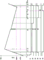
The initialization circuit 500 includes a first voltage detection circuit 501, a timer 502, a second voltage detection circuit 503, an or gate 504, an SR latch 505, a reset circuit 506, and an or gate 507. The initialization circuit 500 functions as an initialization unit for initializing the CPU 202. The initialization circuit 500 starts the process of periodically outputting the initialization signal SR instructing the initialization to the CPU202 when the voltage VDD of the secondary battery 130 drops to or below the first threshold voltage V1 set higher than the operation securing voltage VMIN of the CPU202 and this state continues for a predetermined time T2, and stops the output of the initialization signal SR when the voltage VDD of the secondary battery 130 rises to or above the second threshold voltage V2 (in the present embodiment, V1 < V2) set higher than the operation securing voltage VMIN.
In the present embodiment, the second threshold voltage V2 is set to be higher than the first threshold voltage V1, but it is needless to say that the setting of the threshold voltage may be made to be the same value to reduce the time and effort required for setting the threshold voltage. The length of the predetermined time T2 can be set to a preferable value by performing an experiment as appropriate. In the present embodiment, the length of the predetermined time T2 is set to be shorter than the time required for the voltage VDD of the secondary battery 130 to fall from the first threshold voltage V1 to the operation guaranteed voltage VMIN when the electronic timepiece 10A is operated in a state where power is not supplied to the secondary battery 130. Therefore, the occurrence of the runaway state can be reliably prevented.
The first voltage detection circuit 501 compares the voltage VDD of the secondary battery 130 with the first threshold voltage V1, and transmits a signal S6 corresponding to the comparison result to the timer 502. The first voltage detection circuit 501 outputs a signal S6 at an L level when VDD is equal to or less than V1, and outputs a signal S6 at an H level when VDD > V1.
The timer 502 starts counting time when the signal S6 is switched from the H level to the L level, and resets the counted time and stops counting time when the signal S6 is switched from the L level to the H level. The timer 502 transmits a differential signal S4 to the or gate 504 when the counted time reaches a predetermined time T2.
The second voltage detection circuit 503 compares the voltage VDD of the secondary battery 130 with the second threshold voltage V2, and transmits a signal S5 corresponding to the comparison result to the reset terminal (denoted by "R" in fig. 4) of the SR latch 505. The second voltage detection circuit 503 outputs a signal S5 at an L level when VDD is equal to or less than V2, and outputs a signal S5 at an H level when VDD is greater than V2.
The oscillation stop signal S1, the signal S2 (differential signal output from the watchdog timer 405), the signal S3 (manual reset signal output from the input/output control circuit 404), and the signal S4 (differential signal output from the timer 502) are sent to the or gate 504. The or gate 504 generates a logical sum signal S11 of the signals S1, S2, S3, and S4, and transmits it to the set terminal (denoted by "S" in fig. 4) of the SR latch 505. The SR latch 505 is set by the signal S11 and transmits the signal S8 of the H level to the reset circuit 506, is reset by the signal S5 (output signal of the second voltage detection circuit 503) and transmits the signal S8 of the L level to the reset circuit 506.
The reset circuit 506 outputs the differential signal S10 to the or gate 507 at the falling edge of the clock signal S9 while the signal S8 is at the H level. The oscillation stop signal S1, the signal S2, the signal S3, and the signal S10 are sent to the or gate 507. The or gate 507 transmits a logical sum signal of the signal S1, the signal S2, the signal S3, and the signal S10 to the CPU202 as the initialization signal SR.
The above is the structure of the electronic timepiece 10A.
(A-2: action)
Next, the operation of the electronic timepiece 10A will be described with reference to fig. 5 and 6.
Fig. 5 is a timing chart showing the operation of the electronic timepiece 10A, and fig. 6 is a timing chart showing the operation of the electronic timepiece 10A. Next, the operation of the electronic timepiece 10A will be described by taking the following case as an example: at the start time of the operation shown in the time charts of fig. 5 and 6 (i.e., at the time of time 0), the secondary battery 130 is in an uncharged state, and during the time period from 0 to t3 and after t7, sunlight is irradiated to the solar panel 135 to charge the secondary battery 130, while the electronic timepiece 10A is placed in a dark place and the secondary battery 130 is not charged during the time period from t3 to t 7.
Since the secondary battery 130 is not charged at the start time of this operation, the voltage VDD of the secondary battery is lower than the oscillation start voltage VSAT at time 0, and the oscillation circuit 301 is in the oscillation stop state. Therefore, the oscillation stop detection circuit 303 outputs the oscillation stop signal S1 at the H level. Since the oscillation stop signal S1 is at the H level, the initialization signal SR output from the or gate 507 is at the H level, and the CPU202 is initialized according to the initialization signal SR.
As described above, in the operation example, during the time 0 to t3, the secondary battery 130 is charged with the electric power generated by the solar panel 135, and the voltage VDD of the secondary battery 130 gradually increases. When the oscillation start voltage VSAT is reached at time t1, the oscillation circuit 301 starts oscillating, and the oscillation stop signal S1 becomes the L level. Therefore, the initialization signal SR output from the or gate 507 also becomes L level, and the reset of the CPU202 is released. However, until the voltage of the secondary battery 130 reaches the second threshold voltage V2, the signal S5 continues to be L level, and the output signal S8 of the SR latch 505 continues to be H level. Therefore, the reset circuit 506 outputs the differential signal S10 at a period T1 (e.g., 4 seconds) in synchronization with the clock signal S9. As a result, the CPU202 is reset in the period T1.
Since the voltage VDD exceeds the second threshold voltage V2 at time t2, the second voltage detection circuit 503 switches the signal S5 from the L level to the H level. Thereby, the SR latch 505 is reset, the signal S8 becomes L level, and the differential signal S10 output from the reset circuit 506 continues to be L level. This releases the periodic reset of the CPU202, and the CPU202 enters a normal operating state. Thereafter, the charging of the solar panel 135 is continued until time t3, and thus, the voltage VDD of the secondary battery 130 rises as time passes. Since the electronic timepiece 10A is placed in the dark during time t3 to time t7, power is not supplied from the solar panel 135 to the secondary battery 130, and the voltage VDD of the secondary battery 130 gradually decreases.
At time t4, when the alarm sound is made, the current consumed in the alarm is large, and the power supply voltage VDD temporarily drops to the first threshold voltage V1 during the sound of the alarm due to the internal resistance of the secondary battery 130. While the output signal S6 of the first voltage detection circuit 501 is at the L level during this ringing period, the timer 502 does not output the differential signal S4 and the SR latch 505 is not set as long as the alarm ringing period is less than T2. Therefore, the normal operating state of the CPU202 is maintained. In this way, in the electronic timepiece 10A of the present embodiment, unintentional reset due to a temporary decrease in the power supply voltage caused by alarm ringing does not occur.
After the alarm sound ends, the power supply voltage VDD of the secondary battery 130 returns to about the value before the alarm sound, and thereafter gradually decreases with time. Also, when the power supply voltage VDD is lower than the first threshold voltage V1 at time t5, the output signal S6 of the first voltage detection circuit 501 becomes the L level again, and this state continues. Since the duration of this state reaches T2 or more at time T6, a differential signal S4 is output from the timer 502 to the or gate 504. The SR latch 505 is set according to the output signal S11 of the or gate 504, and the output signal S8 of the SR latch 505 becomes H level. Since the output signal S8 of the SR latch 505 is at the H level, the reset circuit 506 outputs the differential signal S10 at the falling edge of the clock signal S9. As a result, or gate 507 outputs initialization signal SR to CPU202 in a period of T1.
Thereafter, until the power supply voltage rises above the second threshold voltage V2, the CPU202 is reset at T1 cycles. In the present operation example, the electronic timepiece 10A is placed under the sunlight again at time t7, and the charging of the secondary battery 130 is started again. Next, since the power supply voltage is restored to the second threshold voltage V2 or higher at time t8, the CPU202 becomes the normal operation. Further, since the CPU202 is reset at the T1 cycle until the power supply voltage recovers above the second threshold voltage V2 at time T8, the aforementioned continuation of the runaway state does not occur.
As described above, according to the present embodiment, in the electronic timepiece 10A using the secondary battery 130, it is possible to prevent the system from being unintentionally initialized due to the temporary decrease in the power supply voltage VDD, and to prevent the runaway state from continuing.
(B: second embodiment)
Fig. 7 is a block diagram showing an electrical configuration example of an electronic timepiece 10B as a second embodiment of the electronic apparatus of the present invention, that is, a configuration example of a control display unit 150 included in the electronic timepiece 10B. The peripheral circuit 400 of the electronic timepiece 10B is implemented by a software module, and the first voltage detection circuit 501 is also implemented by a software module, which is different from the electronic timepiece 10A. In the present embodiment, as shown in fig. 7, in the electronic timepiece 10B, the counter ct that realizes the function of the timer 502 is realized by a part of the RAM 201.
Next, as in the case of the first embodiment, the following description will be given of an operation performed by the CPU202 of the electronic timepiece 10B as an example: after time 0 to t3 and t7, the solar panel 135 is irradiated with sunlight to charge the secondary battery 130, and during time t3 to t7, the electronic timepiece 10B is placed in the dark and the secondary battery 130 is not charged. In the operation example described below, secondary battery 130 is not charged at the operation start time (i.e., at the time 0).
Fig. 8 is a timing chart showing the operation of the electronic timepiece 10B, and fig. 9 is a flowchart showing the flow of the operation executed by the CPU202 in a 1-second cycle. The signal S6 in fig. 8 corresponds to the determination result of step SA040 in fig. 9. That is, the H-level signal S6 indicates that the determination result of step SA040 is "no", and the L-level signal S6 indicates that the determination result of step SA040 is "yes".
The operation until time t4 is the same as that in the first embodiment, and therefore, the description thereof is omitted. When the alarm sound time is reached at time t4, the determination result at step SA010 in fig. 9 is yes and the alarm sounds thereafter until the alarm sound period ends (step SA 020). Since the current consumption is large in the alarm, the power supply voltage VDD temporarily falls to less than the second threshold voltage V2 due to the internal resistance of the secondary battery 130 during the alarm sound period, the determination result in step SA040 is yes, and the CPU202 counts the counter ct (step SA 080). However, since the alarm sound period is less than T2, the power supply voltage is restored to the second threshold voltage V2 or higher until ct ≧ T2. Therefore, the determination result of step SA090 executed during the alarm sound emission period is always no, and the processing of step SA060 and thereafter is executed. That is, during the alarm sound period, the CPU202 resets the counter ct to 0 (step SA050) and executes other processing and the like (step SA060), and then executes processing of resetting the monitoring timer 405 (step SA070) at a 1-second cycle. That is, during ct < T2, the watchdog timer 405 is reset every 1 second, and the normal operating state of the CPU202 is maintained. In this way, in the electronic timepiece 10B of the present embodiment, an unintended reset does not occur due to a temporary decrease in the power supply voltage caused by an alarm sound.
The time voltage VDD becomes lower than the first threshold voltage V1 by time T5, and thus the count-up of the counter ct is started again, at time T6, ct being T2. Thereafter, the CPU202 repeatedly executes an instruction (nop) not to do any operation (step SA100), and does not perform the reset of the watchdog timer 405 any more. Therefore, the watchdog timer 405 outputs the differential signal S2 3 seconds after the start of counting. The or gate 504 that has accepted the differential signal S2 transmits the signal S11 of the H level to the SR latch 505. The SR latch 505 is set according to the output signal S11 of the or gate 504, and the output signal S8 of the SR latch 505 becomes H level. Since the output signal S8 of the SR latch 505 is at the H level, the reset circuit 506 outputs the differential signal S10 at the falling edge of the clock signal S9, whereby the CPU202 is reset. The following operation is the same as the first embodiment.
As described above, according to the present embodiment, in the electronic device using the secondary battery, it is possible to prevent the system from being unintentionally initialized due to the temporary voltage drop, and to prevent the system from running away due to the continuation of the state in which the charging current is lower than the consumption current.
(C: deformation)
While the first and second embodiments of the present invention have been described above, it is needless to say that the following modifications can be applied to the present embodiment.
(1) When the voltage VDD of the secondary battery 130 becomes lower than the first threshold voltage V1, a part of the functions of the electronic timepiece 10A (or the electronic timepiece 10B) may be stopped. Specifically, when the voltage VDD of the secondary battery 130 becomes lower than the first threshold voltage V1, the function with a large power consumption, such as the alarm sound function in each of the above embodiments, is stopped. When the function with a large power consumption amount is operated in a state where the voltage VDD of the secondary battery 130 is lower than the first threshold voltage V1, the time from when the power supply voltage VDD of the secondary battery 130 is lower than the first threshold voltage V1 to when it is lower than the operation guarantee voltage VMIN may be shorter than T2, and the CPU202 may not be prevented from running away. According to the present embodiment, it is possible to prevent the CPU202 from running away due to a heavy load.
In order to ensure that the time from when the voltage VDD of the secondary battery 130 falls below the first threshold voltage V1 to when the voltage VDD falls below the operation guarantee voltage VMIN is not shorter than T2, a part of the functions of the electronic timepiece may be stopped when the voltage VDD of the secondary battery 130 falls below a third threshold voltage V3 set higher than the first threshold voltage V1. According to the function of the electronic timepiece, even if the voltage VDD of the secondary battery 130 exceeds the first threshold voltage V1 at the operation start time, the voltage VDD of the secondary battery 130 may drop sharply due to the power consumption of the function, and the time until the voltage VDD drops below the operation guaranteed voltage VMIN may be shorter than T2. Therefore, a part of the functions of the electronic timepiece is stopped so as to keep a margin (margin).
(2) A threshold voltage (fourth threshold voltage) at the start of operation of the electronic timepiece 10A (or the electronic timepiece 10B) or after system initialization may be set, and the initialization unit may execute processing for periodically outputting the initialization signal SR until the voltage VDD of the secondary battery 130 rises above the fourth threshold voltage at the start of operation of the electronic device or after system initialization. The fourth threshold voltage naturally needs to be set higher than the operation guaranteed voltage VMIN of the control means. The fourth threshold voltage may be a value different from both the first threshold voltage V1 and the second threshold voltage V2, and may be a value equal to at least one of the first threshold voltage V1 and the second threshold voltage V2. If the fourth threshold voltage V4 is set to a value equal to at least one of the first threshold voltage V1 and the second threshold voltage V2, the time and effort required to set the threshold voltage can be reduced, and the manufacturing cost of the electronic timepiece 10A (or the electronic timepiece 10B) can be reduced. Further, if the fourth threshold voltage V4 is set to a value different from the second threshold voltage V2, it is possible to flexibly determine whether or not initialization of the control unit is necessary using different threshold voltages at the time of start of operation or at the time of voltage increase after system initialization and at the time of voltage increase thereafter.
(3) In each of the above embodiments, a case has been described in which the initialization unit starts the process of outputting the initialization signal SR at a constant cycle when the voltage VDD of the secondary battery 130 drops to or below the first threshold voltage V1 and the state continues for a predetermined time. However, the output interval of the initialization signal SR may be changed according to the voltage VDD or the fluctuation range of the voltage VDD. For example, consider the following: a mode in which the larger the difference between the voltage VDD and the second threshold voltage V2, the shorter the output interval of the initialization signal SR; and a mode in which the larger the decrease width of the unit time in the case of the decrease in the voltage VDD, the shorter the output interval of the initialization signal SR is made, and conversely, the larger the increase width of the voltage VDD in the unit time in the case of the increase (or the case of detecting the supply of the secondary battery 130 by the solar panel 135) is, the longer the output interval of the initialization signal SR is made.
The generation of the runaway due to the initialization omission can be prevented by a method of shortening the output interval of the initialization signal SR as the difference between the voltage VDD and the second threshold voltage V2 becomes larger, or a method of shortening the output interval of the initialization signal SR as the decrease width of the voltage VDD per unit time becomes larger. Further, according to the method of increasing the output interval of the initialization signal SR as the rise width of the voltage VDD per unit time increases, it is expected that the normal operation state can be restored quickly without unintentional initialization. In short, the initialization unit may be caused to execute the process of outputting the initialization signal SR at a predetermined timing when the voltage VDD drops to or below the first threshold voltage V1 and the state continues for a predetermined time.
(4) In order to achieve early return to normal operation, a quick start circuit 800 shown in fig. 10 may be provided. The quick start circuit 800 includes a voltage generation unit 801 and a switch 802, wherein the voltage generation unit 801 and the switch 802 are interposed in parallel between the former of a high-potential-side power supply line PVDD connected to a high-potential-side output terminal of the solar panel 135 and a low-potential-side power supply line PVSS connected to a low-potential-side output terminal of the solar panel 135, and a high-potential-side terminal of the secondary battery 130. The high-potential-side power supply line PVDD and the low-potential-side power supply line PVSS are power supply lines for supplying operating power from the secondary battery 130 to the CPU202 and the peripheral circuit 400.
The voltage generation unit 801 is, for example, a diode, and the switch 802 is a transistor switch which is switched on/off by the initialization unit. In the present modification, the initialization unit turns on the switch 802 when the output of the initialization signal SR is started, and turns off the switch 802 when the output of the initialization signal SR is stopped. In the present modification, the second voltage detection circuit 503 compares the potential difference between the high-potential-side power supply line PVDD and the low-potential-side power supply line PVSS with the second threshold voltage V2 as the voltage of the secondary battery 130.
The potential difference between the high-potential-side power supply line PVDD and the low-potential-side power supply line PVSS is equal to the voltage of the high-potential-side terminal of the secondary battery 130 when the switch 802 is on, and is equal to the voltage obtained by adding the voltage generated by the voltage generation unit 801 (the voltage of the portion reduced by the voltage realized by the diode) to the voltage of the high-potential-side terminal of the secondary battery 130 when the switch 802 is off. That is, according to this embodiment, the voltage to be compared with the second threshold voltage V2 is increased by the voltage generation unit 801, and the time until the normal operation is resumed can be shortened.
(5) In the above embodiments, the application example of the present invention to the multifunction solar watch with alarm was described, but the application object of the present invention is not limited to the multifunction solar watch with alarm. For example, in each of the above embodiments, the solar panel 135 is used as the charging means for charging the secondary battery 130, but a manual generator or a self-rotating generator that generates power by rotation of the crown 50 may be used as the charging means. The application object of the present invention is not limited to an electronic timepiece, and may be a smart phone or a tablet terminal. In short, the present invention can be applied to any electronic device having a secondary battery.
Claims (8)
1. An electronic device, characterized in that the electronic device has:
a secondary battery;
a control unit that receives power supply from the secondary battery and performs drive control of one or more other circuits that are driven by the secondary battery; and
an initialization unit that starts a process of outputting an initialization signal instructing initialization to the control unit at a predetermined timing when a voltage of the secondary battery decreases to a value equal to or lower than a first threshold voltage set higher than an operation guaranteed voltage of the control unit and the state continues for a predetermined time, and stops an output of the initialization signal when a voltage of the secondary battery increases to a value equal to or higher than a second threshold voltage set higher than the operation guaranteed voltage of the control unit,
the predetermined time is set to be shorter than a time during which the voltage of the secondary battery decreases from the first threshold voltage to the operation guaranteed voltage when the electronic device is operated in a state where power is not supplied to the secondary battery.
2. The electronic device of claim 1,
the first threshold voltage and the second threshold voltage are equal.
3. The electronic device of claim 1 or 2,
the control unit stops driving of a predetermined circuit among the one or more other circuits when the voltage of the secondary battery is lower than the first threshold voltage or lower than a third threshold voltage set higher than the first threshold voltage.
4. The electronic device of claim 1 or 2,
the initialization unit executes a process of outputting the initialization signal at a predetermined timing until the voltage of the secondary battery rises above a fourth threshold voltage set higher than the operation guaranteed voltage of the control unit, at the start of the operation of the electronic device or after system initialization.
5. The electronic device of claim 4,
the fourth threshold voltage is equal to at least one of the first threshold voltage and the second threshold voltage.
6. The electronic device of claim 1 or 2,
the electronic device further has a monitoring timer for initializing the system when the monitoring timer counts a predetermined time,
the initialization unit resets the time counted by the monitoring timer at a predetermined timing when the voltage of the secondary battery is higher than the first threshold voltage, and suspends the reset of the monitored time when a state in which the voltage of the secondary battery has dropped below the first threshold voltage continues for the predetermined time or longer.
7. The electronic apparatus according to claim 1 or 2, further having a voltage generating unit and a switch interposed in parallel between the former of a high-potential side power supply line and a low-potential side power supply line for supplying electric power to the one or more other circuits and the control unit, and a high-potential side terminal of the secondary battery,
the initialization unit turns off the switch when the output of the initialization signal is started, turns on the switch when the output of the initialization signal is stopped, and compares the potential difference between the high-potential-side power line and the low-potential-side power line with the second threshold voltage as the voltage of the secondary battery.
8. An initialization method of a control unit of an electronic device, the electronic device having: a secondary battery; one or more other circuits driven by power supplied from the secondary battery; and the control unit that receives power supply from the secondary battery and performs drive control of the one or more other circuits,
starting a process of transmitting an initialization signal instructing initialization to the control unit at a predetermined timing when the voltage of the secondary battery decreases to a value equal to or lower than a first threshold voltage set higher than the operation guaranteed voltage of the control unit and the state continues for a predetermined time, and stopping output of the initialization signal when the voltage of the secondary battery increases to a value equal to or higher than a second threshold voltage set higher than the operation guaranteed voltage of the control unit,
the predetermined time is set to be shorter than a time during which the voltage of the secondary battery decreases from the first threshold voltage to the operation guaranteed voltage when the electronic device is operated in a state where power is not supplied to the secondary battery.
Applications Claiming Priority (2)
| Application Number | Priority Date | Filing Date | Title |
|---|---|---|---|
| JP2015063355A JP6402664B2 (en) | 2015-03-25 | 2015-03-25 | Electronic device and method for initializing control means of electronic device |
| JP2015-063355 | 2015-03-25 |
Publications (2)
| Publication Number | Publication Date |
|---|---|
| CN106019917A CN106019917A (en) | 2016-10-12 |
| CN106019917B true CN106019917B (en) | 2020-03-06 |
Family
ID=55628849
Family Applications (1)
| Application Number | Title | Priority Date | Filing Date |
|---|---|---|---|
| CN201610097361.1A Active CN106019917B (en) | 2015-03-25 | 2016-02-23 | Electronic device and method for initializing control unit of electronic device |
Country Status (4)
| Country | Link |
|---|---|
| US (1) | US9990017B2 (en) |
| EP (1) | EP3073332B1 (en) |
| JP (1) | JP6402664B2 (en) |
| CN (1) | CN106019917B (en) |
Families Citing this family (4)
| Publication number | Priority date | Publication date | Assignee | Title |
|---|---|---|---|---|
| USD812508S1 (en) * | 2017-03-17 | 2018-03-13 | Citizen Watch Co., Ltd. | Dial trim ring for watches |
| JP6848579B2 (en) * | 2017-03-23 | 2021-03-24 | セイコーエプソン株式会社 | Electronic circuits and electronic clocks |
| JP7200512B2 (en) | 2018-06-21 | 2023-01-10 | カシオ計算機株式会社 | ELECTRONIC DEVICE, ELECTRONIC WATCH AND BATTERY CHARGING METHOD |
| JP7359047B2 (en) * | 2020-03-16 | 2023-10-11 | セイコーエプソン株式会社 | real time clock device |
Citations (5)
| Publication number | Priority date | Publication date | Assignee | Title |
|---|---|---|---|---|
| JPH01202673A (en) * | 1988-02-08 | 1989-08-15 | Fujitsu Ltd | Momentary interruption detecting circuit |
| JPH01267756A (en) * | 1988-04-20 | 1989-10-25 | Nippon Denso Co Ltd | Computer control device |
| JPH116885A (en) * | 1997-06-16 | 1999-01-12 | Seiko Epson Corp | Electronic apparatus provided with generator means |
| CN1298131A (en) * | 1999-11-24 | 2001-06-06 | 精工爱普生株式会社 | Electronic chronometer and its controlling method |
| CN1782952A (en) * | 2004-11-29 | 2006-06-07 | 精工爱普生株式会社 | Electronic apparatus and control method thereof |
Family Cites Families (5)
| Publication number | Priority date | Publication date | Assignee | Title |
|---|---|---|---|---|
| DE60123403T2 (en) | 2000-08-11 | 2007-08-23 | Seiko Epson Corp. | ELECTRONIC DEVICE AND METHOD FOR CONTROLLING THEREOF |
| JP4729820B2 (en) * | 2000-08-11 | 2011-07-20 | セイコーエプソン株式会社 | Electronic device and control method of electronic device |
| JP5499872B2 (en) * | 2010-04-21 | 2014-05-21 | ソニー株式会社 | Battery control device, battery control method and program |
| JP2013169094A (en) * | 2012-02-16 | 2013-08-29 | Konica Minolta Inc | Electronic apparatus and power supply unit |
| KR20150038145A (en) * | 2012-09-21 | 2015-04-08 | 닛산 지도우샤 가부시키가이샤 | Charging control device and charging time calculation method |
-
2015
- 2015-03-25 JP JP2015063355A patent/JP6402664B2/en active Active
-
2016
- 2016-02-11 US US15/041,411 patent/US9990017B2/en active Active
- 2016-02-23 CN CN201610097361.1A patent/CN106019917B/en active Active
- 2016-03-23 EP EP16161939.0A patent/EP3073332B1/en active Active
Patent Citations (5)
| Publication number | Priority date | Publication date | Assignee | Title |
|---|---|---|---|---|
| JPH01202673A (en) * | 1988-02-08 | 1989-08-15 | Fujitsu Ltd | Momentary interruption detecting circuit |
| JPH01267756A (en) * | 1988-04-20 | 1989-10-25 | Nippon Denso Co Ltd | Computer control device |
| JPH116885A (en) * | 1997-06-16 | 1999-01-12 | Seiko Epson Corp | Electronic apparatus provided with generator means |
| CN1298131A (en) * | 1999-11-24 | 2001-06-06 | 精工爱普生株式会社 | Electronic chronometer and its controlling method |
| CN1782952A (en) * | 2004-11-29 | 2006-06-07 | 精工爱普生株式会社 | Electronic apparatus and control method thereof |
Also Published As
| Publication number | Publication date |
|---|---|
| JP6402664B2 (en) | 2018-10-10 |
| EP3073332B1 (en) | 2020-11-25 |
| US20160282817A1 (en) | 2016-09-29 |
| EP3073332A1 (en) | 2016-09-28 |
| US9990017B2 (en) | 2018-06-05 |
| CN106019917A (en) | 2016-10-12 |
| JP2016183878A (en) | 2016-10-20 |
Similar Documents
| Publication | Publication Date | Title |
|---|---|---|
| CN106019917B (en) | Electronic device and method for initializing control unit of electronic device | |
| JP5919005B2 (en) | Electronic clock | |
| EP1026559B1 (en) | Electronic watch with generating function | |
| US9092015B2 (en) | Electronic timepiece | |
| JP5025070B2 (en) | Electronic clock | |
| US20130194897A1 (en) | Electronic timepiece | |
| EP2163954B1 (en) | Electronic Timepiece | |
| KR100673927B1 (en) | Electronic device and control method thereof | |
| US8721170B2 (en) | Stepping motor control circuit, movement, and analogue electronic timepiece | |
| US9729095B2 (en) | Stepping motor control circuit, semiconductor device, and analog electronic timepiece | |
| JP6204855B2 (en) | Electronics | |
| JPH1152035A (en) | Variation trend indicator of storage energy, electronic apparatus and electronic watch | |
| KR100880347B1 (en) | Analog electronic watch having a time reset device following power shortage | |
| JP5485759B2 (en) | Information display device | |
| JP6610048B2 (en) | Semiconductor device and electronic timepiece | |
| US10256810B2 (en) | Electronic circuit and electronic timepiece | |
| JP2006337380A (en) | Timepiece with radio-wave correction function | |
| JPH1152081A (en) | Electronic apparatus | |
| JPH1152082A (en) | Electronic timepiece | |
| JP2569039B2 (en) | Electronic clock with warning display | |
| JP6364870B2 (en) | Electronic circuits, watches, and electronic equipment | |
| JP2002022853A (en) | Electronic watch with warning display and its control method | |
| JP7193281B2 (en) | Clocks, electronic devices, and methods of determining illuminance for clocks | |
| JPH0990066A (en) | Electronic clock with power generating mechanism | |
| JP2002250782A (en) | Electronic timepiece with generator |
Legal Events
| Date | Code | Title | Description |
|---|---|---|---|
| C06 | Publication | ||
| PB01 | Publication | ||
| SE01 | Entry into force of request for substantive examination | ||
| SE01 | Entry into force of request for substantive examination | ||
| GR01 | Patent grant | ||
| GR01 | Patent grant |