CN1055588C - Process and architecture for digital micromirror printer - Google Patents
Process and architecture for digital micromirror printer Download PDFInfo
- Publication number
- CN1055588C CN1055588C CN94103181A CN94103181A CN1055588C CN 1055588 C CN1055588 C CN 1055588C CN 94103181 A CN94103181 A CN 94103181A CN 94103181 A CN94103181 A CN 94103181A CN 1055588 C CN1055588 C CN 1055588C
- Authority
- CN
- China
- Prior art keywords
- pixel
- exposure
- pulse
- spatial light
- unit
- Prior art date
- Legal status (The legal status is an assumption and is not a legal conclusion. Google has not performed a legal analysis and makes no representation as to the accuracy of the status listed.)
- Expired - Fee Related
Links
Images


Classifications
-
- H—ELECTRICITY
- H04—ELECTRIC COMMUNICATION TECHNIQUE
- H04N—PICTORIAL COMMUNICATION, e.g. TELEVISION
- H04N1/00—Scanning, transmission or reproduction of documents or the like, e.g. facsimile transmission; Details thereof
- H04N1/40—Picture signal circuits
- H04N1/40025—Circuits exciting or modulating particular heads for reproducing continuous tone value scales
- H04N1/40031—Circuits exciting or modulating particular heads for reproducing continuous tone value scales for a plurality of reproducing elements simultaneously
-
- H—ELECTRICITY
- H04—ELECTRIC COMMUNICATION TECHNIQUE
- H04N—PICTORIAL COMMUNICATION, e.g. TELEVISION
- H04N1/00—Scanning, transmission or reproduction of documents or the like, e.g. facsimile transmission; Details thereof
- H04N1/04—Scanning arrangements, i.e. arrangements for the displacement of active reading or reproducing elements relative to the original or reproducing medium, or vice versa
- H04N1/19—Scanning arrangements, i.e. arrangements for the displacement of active reading or reproducing elements relative to the original or reproducing medium, or vice versa using multi-element arrays
- H04N1/195—Scanning arrangements, i.e. arrangements for the displacement of active reading or reproducing elements relative to the original or reproducing medium, or vice versa using multi-element arrays the array comprising a two-dimensional array or a combination of two-dimensional arrays
Landscapes
- Engineering & Computer Science (AREA)
- Multimedia (AREA)
- Signal Processing (AREA)
- Mechanical Light Control Or Optical Switches (AREA)
- Printers Or Recording Devices Using Electromagnetic And Radiation Means (AREA)
- Color, Gradation (AREA)
- Facsimile Image Signal Circuits (AREA)
Abstract
Techniques for achieving high resolution, high-speed gray scale printing with binary spatial light modulators. A spatial light modulator array is divided into subarrays, and the subarrays are illuminated at various levels (510, 512, 514, 516) of a modulated light source. Additionally, each pixel (520) can be divided up into four phases and printed in phase pairs.
Description
The present invention relates to printing machine, relate in particular to the printing machine that adopts spatial light modulator (SLM).
A discrete component array typically is made up of spatial light modulator.These arrays for example have LCD (LCD) and digital micromirror spare (DMD).Some SLM is binary device, and promptly its each unit or be " conducting " or for " ending " has some then some level can be arranged in addition.In the print system that produces the progressive series of greys (also claiming gray scale), this will produce some problem.
Xerographic printing system typically adopts following method.Printing machine receives from original image, such as terminal or scanned data in order to the scanning element of reproduced image.Print system is converted to light signal with these data, and the illumination of correct pattern is mapped on the photosensitive magnetic drum, forms potential charge pattern on magnetic drum.Then, the toner distributor is passed through in the magnetic drum rotation, and the toner powder is attracted on the lip-deep sub-image of magnetic drum.The magnetic drum band these toner powders and is rotated together, and they are transferred to bottom, promptly is generally on a piece of paper.Then, generally by heat toner is melted on the paper, paper withdraws from printing machine subsequently.
Usually, this type systematic of great majority all adopts the laser scanning exposure system to realize good printing.Because spatial light modulator may provide more printing functionality, is the best so use.Laser scanning system passes through along grating line scanning laser beam printing pixel one by one.For example, if the user wants the speed by 40 pages of per minutes, with the paper of the density printing 8.5 " * 11 " of 600 point/inches (dpi), so every page will require to print 11, and " * 600dpi i.e. 6600 row.Per minute promptly is equivalent to per second 4400 row for 40 pages, and wherein every row has 8.5 * 600 to be 5100 pixels.So just require per second to have 22.44 * 10
6Pixel, 44.6 nanoseconds of each pixel times spent.But laser can not provide the gray scale exposure with the analog form modulation apace in short picture point time.Because SLM has a large amount of optical modulation elements that can work simultaneously, so they can be arranged to print the full line printing information at every turn.The amount of pixels of printing each second is kept identical, but the SLM method provides the time that reaches 5100 times (5100 * 44.6 nanoseconds=227.5 microseconds) to print single pixel with gray modulation.
Yet SLM has the problem of himself, owing to the character of its conduction and cut-off or some level working methods, produces gray scale and promptly becomes quite difficult in full conducting (deceiving) and by producing shade of gray between (no toner) image.Each element all has consistent advantages such as spot diameter, shape and position, obtains the high-quality distinct image thus.Yet because fixing exposure level and location of pixels restriction, resolution can easily be accomplished for example SLM array of 300dpi, also is difficult to reproduce curvilinear figure and trickle text feature.
Therefore, addressing the above problem provides a chance, that is, make print system have better quality, lower price and be easier to performances such as maintenance.
Disclosed print system combines capable integration, pulse-ampli tude modulation, pulse-width modulation and pulse-position modulation, to realize the more printing of high-quality.But this system adopts modulated light source, spatial light modulator and photosensitive medium, and the typical available organophotoreceptorswith of the latter, still, same method also is applicable to thin film dielectrics.
In order more completely to understand the present invention and further advantage thereof, the invention will be further described below with reference to accompanying drawing and detailed explanation.
Fig. 1 represents row integration printing figure;
Fig. 2 a-2f represents to describe the figure of several routine pulse-ampli tude modulations;
Fig. 3 a-3c describes pulse-width modulation;
Fig. 4 represents the pulse-position modulation schematic diagram;
Fig. 5 represents the combination of a routine pulse-position modulation and pulse-ampli tude modulation.
Spatial light modulator typically comprises a cell array, and each array all has its oneself device for addressing.Certain modulator, (DMD) includes memory cell such as digital micromirror spare, and it can receive and store the next frame data, shows current data simultaneously.These data that just allow to be used for any pixel between different unit, even different row and the row unit between " moving ".Data in fact " do not move ", but place the position different with existing display position in the next frame data.This feature allows to utilize many different technology in using such as gray scale printing.
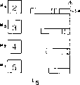
Fig. 1 represents a calcspar of row integration printing, prolongs the time for exposure of any batch data with existing a kind of technology.At t
1, the data that expression is used for the first module of spatial light modulator (SLM) array row 114 are positioned at unit 110.These data are represented with A.Arrow 112 expression printed mediums are such as the photosensitive magnetic drum motion of this column unit 114 relatively.Data A transfers on the medium with an exposure cycle.This single exposure cycle is with display image 118 expressions.
At t
2, perhaps, perhaps re-enter modulator by the data A that will move to reposition by the direct transfer of device inside, make data A arrive the new data input unit 110 that 116, one of unit are designated as B along array.Bar chart on the motion arrow 112 has had change.Image shown in the B 120 has been made single exposure, and A shown in image 118 made re-expose.This process is at t
3Repeat, wherein the image 118 of A has been done three exposures, and the image 120 of B has been made re-expose, and the new data that is designated as C in the unit 110 has single exposure image 122.Certainly, this process can repeat repeatedly, is to obtain the needed exposure frequency of suitable exposure by designer's decision.
In one embodiment of the invention, the integration of will going combines with volume illumination chopping phase, to form gray level image.The capable integration method of prior art allows to form gray level image (being 16 tonal gradations of the capable realization of available 16 integrations) by the number of times that changes in order to the whole integration step of the given pixel of exposing.The present invention is in conjunction with the modulation of row integration and volume illumination, and permission is with few row (exposure of 42 system weightings provides 16 tonal gradations) or higher precision (16 row have 15 full exposures and 1 half exposure provides 32 tonal gradations).
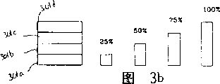
Fig. 2 a-2f represents an example.In this example, this embodiment supposes the reflective spatial light modulator of employing such as digital micromirror spare (DMD) class, and certainly, any binary spatial light modulator with fast response time all can be used.DMD can have multiple different specification, and the fixed DMD of this official holiday has 4 row, one 4 reflector row only is shown, as a time course among the figure.Fig. 2 a is illustrated in t
1Produce the 4 reflectors row of tonal gradation, wherein have only first elementary area to accept its data.In this time frame, light source all illuminates.Print column center M
1In first elementary area of numeral 1 expression printing image or the data of pixel.
Fig. 2 b represents, at t
2, the light source such as light-emitting diode (LED) class illuminates this row with 1/2nd of its whole illumination.The paper epigraph of position 1 has moved to be positioned at reflector M
2Row in, the spitting image of above-described capable integration.Yet at that point, pixel 1 has been accepted 1 full illumination pulse and one 1/2 illumination pulse.With respect to the printing image, represent its all illumination pulse of accumulation with bar shaped 206.In this printing image, pixel 2 is located immediately under the pixel 1, and it has accepted 1/2 illumination pulse, represents with bar shaped 208.
The actual whole illumination of pixel 1 on the paper epigraph can yes or no 1 and 1/2 illumination pulse.At t
1, reflector 1 can be open-minded, allows 1 illumination pulse, at t
2, reflector 2 can cut out, stays actual illumination with 1 illumination pulse on paper.Total this speech of accumulation illumination pulse only means that pixel might accept this illumination.By the four lines reflector, total illumination may be 1.875 times of maximal illumination.Promptly 1 is full illumination pulse, and 0.5 is the second illumination pulse, and 0.25 is the 3rd illumination pulse, and 0.125 is the 4th illumination pulse, is accumulated as 1.875.
Referring now to Fig. 2 c,, modulation of source is arrived 1/4 of its full power.At this moment, be positioned at reflector M
3Pixel 1 have 1.75 total illumination pulse 206.Equally, in Fig. 2 d, pixel 1 has been passed through its all possible light illumination, and shown in bar shaped 206, it has the whole of 1.875 times of full power illumination may illumination.Notice that shown in bar shaped 208, the 1/2+1/4+1/8 that pixel 2 has been accepted total effective illumination pulse is 0.875.In Fig. 2 e, when pixel 2 at t
5When accepting full illumination pulse, promptly finish its possible combination.Also note that shown in 4 pixels after, the next pixel in these row i.e. the 5th pixel begins to move through tonal gradation.
Preferably not in array, these data are sent to formatted memory cell to the data format of suitable this scheme, and pulse-ampli tude modulation is worked.It is shown among Fig. 2 f.These data format as shown like that.At time t
1, such as the data of 0 above three unit, position not shown (numeral of data bit represents that with subscript wherein, 0=is used for the data bit of full illumination, or the like), for pixel 1 (the pixel numeral is used the mark expression) with 0 filling.Exposure represents along the bottom transverse axis, for example E
FRepresent full exposure.
Last example provides 16 possible tonal gradations.4 kinds of different illumination intensities, 16 (2 can be accepted or not accept to each pixel selectively
4) plant possible combination.For the tonal gradation number is increased to 32, only need to increase an additional illumination level, promptly 1/16 of full illumination, and pixel column is combined as 5.Can make up any line number, it only depends on the qualification of system.In addition, being combined as 4 subclass can repeat, and the original resolution of twice is provided, and promptly 32 grades are as follows.
Table 1
| 4 levels of exposure step-length=0.125 | The twice of 4 levels of exposure (step-length=0.125 | ||
| Power (PWR) | Resolution | Power (PWR) | |
| 1 | 8 | 1 | 8 |
| .5 | 4 | .5 | 4 |
| .25 | 2 | .25 | 2 |
| .125 | 1 | .125 | 1 |
| 1 | 8 | ||
| .5 | 4 | ||
| .25 | 2 | ||
| .125 | 1 | ||
| 1.875 | 15 | 3.75 | 30 |
Last table explanation, resolution depend on how many steps are this method can reach.Come again by the pattern that Fig. 2 a-2f is discussed, can improve power and resolution.According to the required power of system and the complexity of addressing circuit, this circuit must be able to be formatd data suitably, could realize multiple different combination.Sometimes need data are carried out the format of higher degree, in to big power and high-resolution.In addition, can reach medium resolution, obtain high-power simultaneously by a grade of eliminating in the levels of exposure.Next is opened table this problem has been described.Notice that speech " grade " refers to level of illumination rather than tonal gradation.
| 4 | 4 grades of twice | Power in the high-resolution | Intermediate-resolution is high-power | |||||
| Power | Resolution | Power | Resolution | Power | | Power | Resolution | |
| 1 | 8 | 1 | 8 | 1 | 8 | 1 | 4 | |
| .5 | 4 | .5 | 4 | 1 | 8 | 1 | 4 | |
| .25 | 2 | .25 | 2 | 1 | 8 | 1 | 4 | |
| .125 | 1 | .125 | 1 | 1 | 8 | 1 | 4 | |
| 1 | 8 | 1 | 8 | 1 | 4 | |||
| .3 | 4 | .5 | 4 | 1 | 4 | |||
| .25 | 2 | .25 | 2 | .5 | 2 | |||
| .125 | 1 | .125 | 1 | .25 | 1 | |||
| 1.875 | 15 | 3.75 | 30 | 5.875 | 47 | 6.75 | 27 | |
So far, these technology are all being imagined a kind of uniform pixel wide through on the direction.In the time can forming the pixel cell of different in width, in binary space light modulation printing, just can realize more flexibility.This can realize that although square pixel is enough, these two kinds of methods all will be benefited from the use of rectangular pixels with two kinds of methods.These technology are called pulse-width modulation.
Fig. 3 a represents first method.In this embodiment, we adopted depth-width ratio to rectangular pixels, as 4: 1.In addition, rectangular pixels is 3 reflecting parts at interval, shown in frame 301, and 4 reflector segment of reflector row of its expression.In this example, have only the reflector of opening to be used in the row section 301.By one different period an of bright light source, can be at this through forming the pixel cell of different in width on direction.
The length 306 of image 304 pixels of expression on a piece of paper, and be illuminated 25% of a whole line time corresponding to the array element of this image.Certainly, this is to suppose that it is 1 that this image is wanted data presented.If data are 0, will there be image.When unit of image 308 expressions illuminated for 50% time, the length 310 of this pixel image.Equally, image 312 and 316 expressions 75% are illuminated the time and 100% and are illuminated the respective length of time.
According to 4: 1 depth-width ratios of reality, active reflector should 3 be gone at interval with other reflector, to form whole 4 pulsewidths on photosensitive medium.This is similar to a figure shown in Fig. 2 f with employing, but subscript should be called pulsewidth now, rather than pulse amplitude.Subscript 0 is 25% width, and subscript 1 is 50% width, or the like.
Note, by only utilizing delegation's reflector, and data on the toggle reflections device rather than toggle lights, can obtain same effect.Yet this need be in the time of delegation packs data in the row into for 4 times, and each line time of original scheme only needs once.This two embodiment have comprised respectively and have activated and the notion of non-activation unit, perhaps by the physical method in the following method, perhaps as in the above-mentioned method, the usefulness photoactivation they.
Fig. 3 b represents to reach the second method that has same effect with pulse-width modulation with the illumination pulse with equal length.In the method, the reflector of a plurality of adjacency has the printing position of different in width in order to formation.In the example of 4: 1 depth-width ratios, it has used 4 row, but does not skip any reflector.By on-unit 301a, the printing position will have and the identical width in 25% pulse-width modulation position.Connect 301a and 301b, width equals 50% pulsewidth, connects 301a-301c and equals 75% pulsewidth, connects 301a-301d, then equals 100% pulsewidth.For it was had accurate 1: 2: 3: 4 ratio and not fuzzy basically, light must have near 0% duty cycle, shown in Fig. 3 b.Because moving of photosurface, higher duty cycle will produce fuzzy and have influence on the peak pulse duration that is produced.
Two kinds of methods that are used for pulse-width modulation all have benefited from the use of rectangular pixels.Rectangular pixels or be taken from rectangular element on the spatial light modulator array with isomorphism optics perhaps is taken from the square pixel with synthesizing optical.Synthesizing optical has compressed the vertical component of square pixel, such as DMD, and natural with it on horizontal component.So just formed the spitting image of a kind of rectangular pixels described in the pulse-width modulation.Yet, in order to realize this measure, should make a kind of special array, the interval width that its reflector is capable equals Pixel Dimensions and multiply by synthetic compression ratio (for example, for 4: 1 the ratio of width to height, line-spacing should be the width of 4 pixels).This will allow the pulsewidth printing, and can overlapping printed pixels.Notice that for the actual pulse-width modulation shown in Fig. 3 a, this particular array will be unique essential.Fig. 3 b adopts the reflector of adjacency, does not therefore need this special array.
Pulse-width modulation can change to realize pulse-position modulation, wherein, and constant width, but light source service time delay.Fig. 3 C has represented an example in this.Zero-time is delayed, and by 4 kinds of different time representations, allows pulse to be added in the diverse location of medium.Each exposure 320a-320d all is called as a phase place.
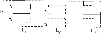
Fig. 4 represents a kind of phase method for position, and it allows a pixel image is divided into several phase places, and prints non-overlapped phase place together.4 phase places of this example, but the phase place of other quantity, for example 6 phase places also can adopt.Wherein, the first, the 3rd and the 5th phase place is printed together, and the second, the 4th and the 6th phase place is printed together.In other words, in the time that is used for 3 exposures, pixel can be printed two phase places.Macroscopic view pixel P has 4 phase place Φ 1 to Φ
4At t
1, because they depart from phase place Φ mutually
1And Φ
3Together with the rectangular in form printing.At t
2, phase place Φ
2And Φ
4Printing together.This process allows with two steps rather than four 4 phase places that step is printed macroscopical pixel P, at t
3Form image.According to the concentration of toner, broad or narrower pixel can show as gray scale.The combination of multiple concentration toner, combining with the ability of selecting phase place in a macroscopical pixel provides higher flexibility when forming gray scale.
Adopt binary spatial light modulator, the gray scale that above-mentioned technology can combination results high-resolution (600dpi).Fig. 5 represents combining of pulse-ampli tude modulation and pulse-position modulation.One of four exposure level represented respectively in every group of bracket 510,512,514,516 and 518.For ease of discussing, will cross medium and follow the trail of pixel 1 (520).Notice that the motion on the vertical direction is the process direction of medium, is the time along moving of horizontal direction.Represent that around the right frame of broken lines of pixel how overlapping phase place is when printing.
Pixel 1 (520) is exposed with whole power when phase place 1 and 3 in the left column of bracket 510.3/4ths line time (is used time interval t on time shaft 530
1Expression) afterwards, phase place 2 and 4 is with whole power exposures.This time delay must compensate 1/4 of line time, with allow two phase places between 1/4 pixel adjustment, cause t
1Equal 3/4 line time, as shown in Figure 4.In the above-mentioned discussion, phase place can be opened or close, and exposure only represents that light transferred to the possibility on the magnetic drum.
The macroscopic view pixel is now in all four phase places, or two phase place centerings are by full illumination exposure.Bracket 512 expressions are with 1/2 full illumination exposure.Time delay between the bracket 510 and 512 is used time interval t on time shaft
2Expression, it is 5/4 line time.Now, pixel is transferred to next unit or formed next group unit of macroscopical pixel, and is as shown in Figure 2.Need equally 1/4 additional line time finish phase place between adjustment.This process repeats along the line 524 that is used for this specific macroscopical pixel, and is right with the phase place of 1/8 illumination level until receiving in bracket 518.To this, should organize row, finished specific macroscopical pixel.Table is described in the reference, and pixel can receive that group row of repetition.
Notice that at the right side of bracket 510 row, the phase place 2 of pixel 2 is exposed.Then, identical with the process of pixel 1 (520), just phase place 4 is just accepted the exposure of whole power up to the right side of bracket 518 row, position 526.This circulation occur in one row in each pixel between.Present technique is not limited to 4 pixels.As previously mentioned, it can adopt many pixels according to designer's needs, and only is subject to the performance range of array and electronics.
Although more than described the embodiment that carries out gray scale printing with binary spatial light modulator, they are not to be used for limiting the scope of the invention, and scope of the present invention is the represented scope of appended claims.
Claims (10)
1. the pulse-ampli tude modulation method of the spatial light modulator of a printing machine is characterized in that comprising:
A) provide the spatial light modulator array with subarray, it comprises predetermined line number;
B) will be added in order to visit the addressing circuit of a unit of described array corresponding to the data of the exposure of a used light source of pixel;
C) make the exposure of described unit according to described exposure, selectively with described data imaging or be not imaged on the photosensitive medium;
D) add and the corresponding data of described light source next one exposure, wherein, described data can be added to the circuit that is used for different units, with the motion of coordinating data described in the described subarray and the motion of described medium;
E) make the exposure of described unit according to described next exposure, selectively with described data imaging or be not imaged on the described photosensitive medium, and
F) repeat to add data and make the unit step of exposing, till described unit being exposed according to the exposure of each predetermined quantity.
2. the method for claim 1 is characterized in that, described spatial light modulator comprises digital micromirror spare.
3. the method for claim 1 is characterized in that, described predetermined line number equals four.
4. the pulse duration modulation method of the spatial light modulator of a printing machine is characterized in that comprising:
A) determine a macroscopical pixel, it comprises the unit of a predetermined quantity in the spatial light modulator array;
B) subelement of one group of adjacency in the unit of the described predetermined quantity of selection, wherein, its pulsewidth is directly proportional with the size of one group of subelement of described predetermined quantity.
5. method as claimed in claim 4 is characterized in that described spatial light modulator comprises digital micromirror spare.
6. method as claimed in claim 4 is characterized in that, the width by fixing described pulse also postpones the time that described pulse opens and sets described pulse.
7. method as claimed in claim 4, it is characterized in that also comprising a unit that excites in the spatial light modulator array, on a move media, produce a pixel image, and in a preset time interval after the described exciting step, do not excite described unit, wherein, described preset time has determined that at interval pixel is along the size on the direction of motion of described moving medium.
8. method as claimed in claim 7 is characterized in that, described excite and not exciting step finish by opening and close light source respectively.
9. method as claimed in claim 7 is characterized in that, described excite and not exciting step finish by opening and close described unit respectively.
10. the pulse-position modulation method of the spatial light modulator of a printing machine is characterized in that comprising:
A) along a pixel being divided into some phase places through direction, wherein, the inverse of described some phase places in length of each phase deviation adjacent phase, as many as this pixel of this length;
B) make the exposure of of one in described phase place group, wherein, a described son group comprises the phase place that is separated by at least one phase place mutually; And
C) make the phasing exposure that had not before exposed, by finishing exposure for the given illumination of described pixel.
Applications Claiming Priority (2)
| Application Number | Priority Date | Filing Date | Title |
|---|---|---|---|
| US08/038,398 | 1993-03-29 | ||
| US08/038,398 US5461411A (en) | 1993-03-29 | 1993-03-29 | Process and architecture for digital micromirror printer |
Publications (2)
| Publication Number | Publication Date |
|---|---|
| CN1097069A CN1097069A (en) | 1995-01-04 |
| CN1055588C true CN1055588C (en) | 2000-08-16 |
Family
ID=21899726
Family Applications (1)
| Application Number | Title | Priority Date | Filing Date |
|---|---|---|---|
| CN94103181A Expired - Fee Related CN1055588C (en) | 1993-03-29 | 1994-03-29 | Process and architecture for digital micromirror printer |
Country Status (8)
| Country | Link |
|---|---|
| US (1) | US5461411A (en) |
| EP (1) | EP0620676B1 (en) |
| JP (1) | JPH07125317A (en) |
| KR (1) | KR100296067B1 (en) |
| CN (1) | CN1055588C (en) |
| CA (1) | CA2118728A1 (en) |
| DE (1) | DE69424714T2 (en) |
| TW (1) | TW243518B (en) |
Families Citing this family (195)
| Publication number | Priority date | Publication date | Assignee | Title |
|---|---|---|---|---|
| US6219015B1 (en) | 1992-04-28 | 2001-04-17 | The Board Of Directors Of The Leland Stanford, Junior University | Method and apparatus for using an array of grating light valves to produce multicolor optical images |
| US6674562B1 (en) | 1994-05-05 | 2004-01-06 | Iridigm Display Corporation | Interferometric modulation of radiation |
| US5459492A (en) * | 1993-08-30 | 1995-10-17 | Texas Instruments Incorporated | Method and apparatus for printing stroke and contone data together |
| US8014059B2 (en) | 1994-05-05 | 2011-09-06 | Qualcomm Mems Technologies, Inc. | System and method for charge control in a MEMS device |
| US5615016A (en) * | 1994-11-04 | 1997-03-25 | Texas Instruments Incorporated | Exposure scheme for minimizing microbanding inslm-based printers |
| US6074790A (en) * | 1994-11-17 | 2000-06-13 | Texas Instruments Incorporated | Black and white defect correction for a digital micromirror printer |
| US5630027A (en) * | 1994-12-28 | 1997-05-13 | Texas Instruments Incorporated | Method and apparatus for compensating horizontal and vertical alignment errors in display systems |
| US5841579A (en) | 1995-06-07 | 1998-11-24 | Silicon Light Machines | Flat diffraction grating light valve |
| US5699168A (en) * | 1995-06-22 | 1997-12-16 | Texas Instruments Incorporated | Grayscale printing with sliding window memory |
| KR100449129B1 (en) * | 1995-10-25 | 2005-01-24 | 인스트루먼츠 인코포레이티드 텍사스 | Investigation system |
| EP0785524A3 (en) | 1996-01-05 | 1999-01-13 | Texas Instruments Incorporated | Printing with dot shape modulation and greyscale |
| US5841956A (en) * | 1996-01-05 | 1998-11-24 | Texas Instruments Incorporated | Anti-aliasing for digital printing with dot shape modulation and greyscale |
| DE69618163T2 (en) * | 1996-02-09 | 2002-07-04 | Texas Instruments Inc., Dallas | Uniform exposure of a light-sensitive medium with square intensity profiles for printing purposes |
| US7471444B2 (en) | 1996-12-19 | 2008-12-30 | Idc, Llc | Interferometric modulation of radiation |
| US5982553A (en) | 1997-03-20 | 1999-11-09 | Silicon Light Machines | Display device incorporating one-dimensional grating light-valve array |
| AU9805498A (en) | 1997-10-16 | 1999-05-03 | Int Labs, Inc. | Data transfer over wire or wireless medium |
| US6088102A (en) | 1997-10-31 | 2000-07-11 | Silicon Light Machines | Display apparatus including grating light-valve array and interferometric optical system |
| EP0933925A3 (en) * | 1997-12-31 | 2002-06-26 | Texas Instruments Inc. | Photofinishing utilizing modulated light source array |
| WO1999052006A2 (en) | 1998-04-08 | 1999-10-14 | Etalon, Inc. | Interferometric modulation of radiation |
| US8928967B2 (en) | 1998-04-08 | 2015-01-06 | Qualcomm Mems Technologies, Inc. | Method and device for modulating light |
| US6271808B1 (en) | 1998-06-05 | 2001-08-07 | Silicon Light Machines | Stereo head mounted display using a single display device |
| US6130770A (en) | 1998-06-23 | 2000-10-10 | Silicon Light Machines | Electron gun activated grating light valve |
| US6101036A (en) | 1998-06-23 | 2000-08-08 | Silicon Light Machines | Embossed diffraction grating alone and in combination with changeable image display |
| US6215579B1 (en) | 1998-06-24 | 2001-04-10 | Silicon Light Machines | Method and apparatus for modulating an incident light beam for forming a two-dimensional image |
| US6303986B1 (en) | 1998-07-29 | 2001-10-16 | Silicon Light Machines | Method of and apparatus for sealing an hermetic lid to a semiconductor die |
| US6215547B1 (en) | 1998-11-19 | 2001-04-10 | Eastman Kodak Company | Reflective liquid crystal modulator based printing system |
| US6391245B1 (en) | 1999-04-13 | 2002-05-21 | Eom Technologies, L.L.C. | Method for creating three-dimensional objects by cross-sectional lithography |
| WO2003007049A1 (en) | 1999-10-05 | 2003-01-23 | Iridigm Display Corporation | Photonic mems and structures |
| US6330018B1 (en) | 1999-12-22 | 2001-12-11 | Eastman Kodak Company | Method and apparatus for printing high resolution images using reflective LCD modulators |
| JP4052542B2 (en) * | 2000-02-25 | 2008-02-27 | 富士フイルム株式会社 | Printer |
| US6500378B1 (en) | 2000-07-13 | 2002-12-31 | Eom Technologies, L.L.C. | Method and apparatus for creating three-dimensional objects by cross-sectional lithography |
| US6407766B1 (en) | 2000-07-18 | 2002-06-18 | Eastman Kodak Company | Method and apparatus for printing to a photosensitive media using multiple spatial light modulators |
| US6646716B1 (en) | 2000-07-27 | 2003-11-11 | Eastman Kodak Company | Method and apparatus for printing multiple simultaneous images onto a photosensitive media |
| US6552740B1 (en) | 2000-08-01 | 2003-04-22 | Eastman Kodak Company | Method and apparatus for printing monochromatic imaging using a spatial light modulator |
| US6480259B1 (en) * | 2000-09-28 | 2002-11-12 | Eastman Kodak Company | Method and apparatus for printing monochromatic images using a spatial light modulator having a selectable light source |
| JP2002120400A (en) * | 2000-10-17 | 2002-04-23 | Fuji Photo Film Co Ltd | Method and apparatus for image recording |
| US6614462B1 (en) * | 2000-10-19 | 2003-09-02 | Eastman Kodak Company | Method and apparatus for printing high resolution images using reflective LCD modulators |
| US6580490B1 (en) | 2000-10-30 | 2003-06-17 | Eastman Kodak Company | Method and apparatus for printing images in multiple formats using a spatial light modulator |
| EP1206115A3 (en) * | 2000-11-14 | 2004-02-11 | Fuji Photo Film Co., Ltd. | Image recording method and image recording apparatus |
| US6624880B2 (en) | 2001-01-18 | 2003-09-23 | Micronic Laser Systems Ab | Method and apparatus for microlithography |
| US6930797B2 (en) * | 2001-02-27 | 2005-08-16 | Eastman Kodak Company | Method and apparatus for printing high resolution images using multiple reflective spatial light modulators |
| US6707591B2 (en) | 2001-04-10 | 2004-03-16 | Silicon Light Machines | Angled illumination for a single order light modulator based projection system |
| US6747781B2 (en) | 2001-06-25 | 2004-06-08 | Silicon Light Machines, Inc. | Method, apparatus, and diffuser for reducing laser speckle |
| US6782205B2 (en) | 2001-06-25 | 2004-08-24 | Silicon Light Machines | Method and apparatus for dynamic equalization in wavelength division multiplexing |
| US6589625B1 (en) | 2001-08-01 | 2003-07-08 | Iridigm Display Corporation | Hermetic seal and method to create the same |
| US6829092B2 (en) | 2001-08-15 | 2004-12-07 | Silicon Light Machines, Inc. | Blazed grating light valve |
| US6980321B2 (en) * | 2001-08-20 | 2005-12-27 | Eastman Kodak Company | Method and apparatus for printing high resolution images using multiple reflective spatial light modulators |
| US6778290B2 (en) | 2001-08-23 | 2004-08-17 | Eastman Kodak Company | Printing image frames corresponding to motion pictures |
| US6980280B2 (en) * | 2001-10-12 | 2005-12-27 | Eastman Kodak Company | Two level image writer |
| TW556043B (en) | 2001-11-30 | 2003-10-01 | Asml Netherlands Bv | Imaging apparatus, device manufacturing method and device manufactured by said method |
| US6800238B1 (en) | 2002-01-15 | 2004-10-05 | Silicon Light Machines, Inc. | Method for domain patterning in low coercive field ferroelectrics |
| US6855482B2 (en) * | 2002-04-09 | 2005-02-15 | Day International, Inc. | Liquid transfer articles and method for producing the same using digital imaging photopolymerization |
| US6728023B1 (en) | 2002-05-28 | 2004-04-27 | Silicon Light Machines | Optical device arrays with optimized image resolution |
| US6767751B2 (en) | 2002-05-28 | 2004-07-27 | Silicon Light Machines, Inc. | Integrated driver process flow |
| US6822797B1 (en) | 2002-05-31 | 2004-11-23 | Silicon Light Machines, Inc. | Light modulator structure for producing high-contrast operation using zero-order light |
| US6829258B1 (en) | 2002-06-26 | 2004-12-07 | Silicon Light Machines, Inc. | Rapidly tunable external cavity laser |
| US6813059B2 (en) | 2002-06-28 | 2004-11-02 | Silicon Light Machines, Inc. | Reduced formation of asperities in contact micro-structures |
| US6801354B1 (en) | 2002-08-20 | 2004-10-05 | Silicon Light Machines, Inc. | 2-D diffraction grating for substantially eliminating polarization dependent losses |
| KR101087930B1 (en) | 2002-08-24 | 2011-11-28 | 매스크리스 리소그래피 인코퍼레이티드 | Continuous direct-write optical lithography |
| US6734889B2 (en) | 2002-09-10 | 2004-05-11 | Eastman Kodak Company | Color printer comprising a linear grating spatial light modulator |
| US7781850B2 (en) | 2002-09-20 | 2010-08-24 | Qualcomm Mems Technologies, Inc. | Controlling electromechanical behavior of structures within a microelectromechanical systems device |
| US6712480B1 (en) | 2002-09-27 | 2004-03-30 | Silicon Light Machines | Controlled curvature of stressed micro-structures |
| US6751005B1 (en) | 2002-12-20 | 2004-06-15 | Eastman Kodak Company | Compensating for pixel defects by spatial translation of scene content |
| US7369268B2 (en) * | 2003-01-14 | 2008-05-06 | Eastman Kodak Company | Light source using large area LEDs |
| US7417782B2 (en) | 2005-02-23 | 2008-08-26 | Pixtronix, Incorporated | Methods and apparatus for spatial light modulation |
| US6917462B2 (en) * | 2003-02-24 | 2005-07-12 | Eastman Kodak Company | Method and apparatus for translating a spatial light modulator to provide dithering |
| US6829077B1 (en) | 2003-02-28 | 2004-12-07 | Silicon Light Machines, Inc. | Diffractive light modulator with dynamically rotatable diffraction plane |
| US6806997B1 (en) | 2003-02-28 | 2004-10-19 | Silicon Light Machines, Inc. | Patterned diffractive light modulator ribbon for PDL reduction |
| US7042483B2 (en) * | 2003-03-10 | 2006-05-09 | Eastman Kodak Company | Apparatus and method for printing using a light emissive array |
| US6836284B2 (en) * | 2003-04-01 | 2004-12-28 | Tri-Star Technologies | Laser marking using a digital micro-mirror device |
| TW570896B (en) | 2003-05-26 | 2004-01-11 | Prime View Int Co Ltd | A method for fabricating an interference display cell |
| US6975339B2 (en) * | 2003-05-31 | 2005-12-13 | Hewlett-Packard Development Company, L.P. | Electrostatic-writing mechanism having micromirrors to selectively direct light onto optical photoconductor mechanism |
| US7307764B2 (en) * | 2003-07-16 | 2007-12-11 | Eastman Kodak Company | Apparatus and method for controlled movement of pixel imaging device |
| US7023463B2 (en) * | 2003-07-22 | 2006-04-04 | Eastman Kodak Company | Method and apparatus for printing images from digital image data |
| US6999227B2 (en) * | 2003-10-31 | 2006-02-14 | Intel Corporation | Projection system |
| US7012726B1 (en) | 2003-11-03 | 2006-03-14 | Idc, Llc | MEMS devices with unreleased thin film components |
| CA2545686C (en) * | 2003-11-03 | 2011-07-19 | Punch Graphix Prepress Germany Gmbh | A device and method for digital exposure |
| US7161728B2 (en) | 2003-12-09 | 2007-01-09 | Idc, Llc | Area array modulation and lead reduction in interferometric modulators |
| US7142346B2 (en) | 2003-12-09 | 2006-11-28 | Idc, Llc | System and method for addressing a MEMS display |
| US7706050B2 (en) | 2004-03-05 | 2010-04-27 | Qualcomm Mems Technologies, Inc. | Integrated modulator illumination |
| US7224379B2 (en) * | 2004-05-03 | 2007-05-29 | Eastman Kodak Company | Printer using direct-coupled emissive array |
| US7164520B2 (en) | 2004-05-12 | 2007-01-16 | Idc, Llc | Packaging for an interferometric modulator |
| US7889163B2 (en) | 2004-08-27 | 2011-02-15 | Qualcomm Mems Technologies, Inc. | Drive method for MEMS devices |
| US7551159B2 (en) | 2004-08-27 | 2009-06-23 | Idc, Llc | System and method of sensing actuation and release voltages of an interferometric modulator |
| US7560299B2 (en) | 2004-08-27 | 2009-07-14 | Idc, Llc | Systems and methods of actuating MEMS display elements |
| US7515147B2 (en) | 2004-08-27 | 2009-04-07 | Idc, Llc | Staggered column drive circuit systems and methods |
| US7499208B2 (en) | 2004-08-27 | 2009-03-03 | Udc, Llc | Current mode display driver circuit realization feature |
| US7602375B2 (en) | 2004-09-27 | 2009-10-13 | Idc, Llc | Method and system for writing data to MEMS display elements |
| US7724993B2 (en) | 2004-09-27 | 2010-05-25 | Qualcomm Mems Technologies, Inc. | MEMS switches with deforming membranes |
| US7415186B2 (en) | 2004-09-27 | 2008-08-19 | Idc, Llc | Methods for visually inspecting interferometric modulators for defects |
| US7920135B2 (en) | 2004-09-27 | 2011-04-05 | Qualcomm Mems Technologies, Inc. | Method and system for driving a bi-stable display |
| US7916103B2 (en) | 2004-09-27 | 2011-03-29 | Qualcomm Mems Technologies, Inc. | System and method for display device with end-of-life phenomena |
| US7583429B2 (en) | 2004-09-27 | 2009-09-01 | Idc, Llc | Ornamental display device |
| US8008736B2 (en) | 2004-09-27 | 2011-08-30 | Qualcomm Mems Technologies, Inc. | Analog interferometric modulator device |
| US7310179B2 (en) | 2004-09-27 | 2007-12-18 | Idc, Llc | Method and device for selective adjustment of hysteresis window |
| US7372613B2 (en) | 2004-09-27 | 2008-05-13 | Idc, Llc | Method and device for multistate interferometric light modulation |
| US7710629B2 (en) | 2004-09-27 | 2010-05-04 | Qualcomm Mems Technologies, Inc. | System and method for display device with reinforcing substance |
| US7944599B2 (en) | 2004-09-27 | 2011-05-17 | Qualcomm Mems Technologies, Inc. | Electromechanical device with optical function separated from mechanical and electrical function |
| US8124434B2 (en) | 2004-09-27 | 2012-02-28 | Qualcomm Mems Technologies, Inc. | Method and system for packaging a display |
| US7446927B2 (en) | 2004-09-27 | 2008-11-04 | Idc, Llc | MEMS switch with set and latch electrodes |
| US20060176487A1 (en) | 2004-09-27 | 2006-08-10 | William Cummings | Process control monitors for interferometric modulators |
| US7893919B2 (en) | 2004-09-27 | 2011-02-22 | Qualcomm Mems Technologies, Inc. | Display region architectures |
| US7453579B2 (en) | 2004-09-27 | 2008-11-18 | Idc, Llc | Measurement of the dynamic characteristics of interferometric modulators |
| US7679627B2 (en) | 2004-09-27 | 2010-03-16 | Qualcomm Mems Technologies, Inc. | Controller and driver features for bi-stable display |
| US7813026B2 (en) | 2004-09-27 | 2010-10-12 | Qualcomm Mems Technologies, Inc. | System and method of reducing color shift in a display |
| US7355780B2 (en) | 2004-09-27 | 2008-04-08 | Idc, Llc | System and method of illuminating interferometric modulators using backlighting |
| US20060076634A1 (en) | 2004-09-27 | 2006-04-13 | Lauren Palmateer | Method and system for packaging MEMS devices with incorporated getter |
| US8878825B2 (en) | 2004-09-27 | 2014-11-04 | Qualcomm Mems Technologies, Inc. | System and method for providing a variable refresh rate of an interferometric modulator display |
| US7653371B2 (en) | 2004-09-27 | 2010-01-26 | Qualcomm Mems Technologies, Inc. | Selectable capacitance circuit |
| US7675669B2 (en) | 2004-09-27 | 2010-03-09 | Qualcomm Mems Technologies, Inc. | Method and system for driving interferometric modulators |
| US7486429B2 (en) | 2004-09-27 | 2009-02-03 | Idc, Llc | Method and device for multistate interferometric light modulation |
| US7684104B2 (en) | 2004-09-27 | 2010-03-23 | Idc, Llc | MEMS using filler material and method |
| US7626581B2 (en) | 2004-09-27 | 2009-12-01 | Idc, Llc | Device and method for display memory using manipulation of mechanical response |
| US7420725B2 (en) | 2004-09-27 | 2008-09-02 | Idc, Llc | Device having a conductive light absorbing mask and method for fabricating same |
| US7424198B2 (en) | 2004-09-27 | 2008-09-09 | Idc, Llc | Method and device for packaging a substrate |
| US7417735B2 (en) | 2004-09-27 | 2008-08-26 | Idc, Llc | Systems and methods for measuring color and contrast in specular reflective devices |
| US7545550B2 (en) | 2004-09-27 | 2009-06-09 | Idc, Llc | Systems and methods of actuating MEMS display elements |
| US7668415B2 (en) | 2004-09-27 | 2010-02-23 | Qualcomm Mems Technologies, Inc. | Method and device for providing electronic circuitry on a backplate |
| US7719500B2 (en) | 2004-09-27 | 2010-05-18 | Qualcomm Mems Technologies, Inc. | Reflective display pixels arranged in non-rectangular arrays |
| US7289256B2 (en) | 2004-09-27 | 2007-10-30 | Idc, Llc | Electrical characterization of interferometric modulators |
| US7843410B2 (en) | 2004-09-27 | 2010-11-30 | Qualcomm Mems Technologies, Inc. | Method and device for electrically programmable display |
| US7532195B2 (en) | 2004-09-27 | 2009-05-12 | Idc, Llc | Method and system for reducing power consumption in a display |
| US7808703B2 (en) | 2004-09-27 | 2010-10-05 | Qualcomm Mems Technologies, Inc. | System and method for implementation of interferometric modulator displays |
| US7701631B2 (en) | 2004-09-27 | 2010-04-20 | Qualcomm Mems Technologies, Inc. | Device having patterned spacers for backplates and method of making the same |
| US7345805B2 (en) | 2004-09-27 | 2008-03-18 | Idc, Llc | Interferometric modulator array with integrated MEMS electrical switches |
| US7692839B2 (en) | 2004-09-27 | 2010-04-06 | Qualcomm Mems Technologies, Inc. | System and method of providing MEMS device with anti-stiction coating |
| US7289259B2 (en) | 2004-09-27 | 2007-10-30 | Idc, Llc | Conductive bus structure for interferometric modulator array |
| US7359066B2 (en) | 2004-09-27 | 2008-04-15 | Idc, Llc | Electro-optical measurement of hysteresis in interferometric modulators |
| US7936497B2 (en) | 2004-09-27 | 2011-05-03 | Qualcomm Mems Technologies, Inc. | MEMS device having deformable membrane characterized by mechanical persistence |
| US7136213B2 (en) | 2004-09-27 | 2006-11-14 | Idc, Llc | Interferometric modulators having charge persistence |
| US8310441B2 (en) | 2004-09-27 | 2012-11-13 | Qualcomm Mems Technologies, Inc. | Method and system for writing data to MEMS display elements |
| US7369150B2 (en) * | 2005-02-02 | 2008-05-06 | Infoprint Solutions Company, Llc | Method, system and program product for amplitude modulated multiple pel print quality enhancement |
| US9229222B2 (en) | 2005-02-23 | 2016-01-05 | Pixtronix, Inc. | Alignment methods in fluid-filled MEMS displays |
| US9158106B2 (en) | 2005-02-23 | 2015-10-13 | Pixtronix, Inc. | Display methods and apparatus |
| US7304785B2 (en) | 2005-02-23 | 2007-12-04 | Pixtronix, Inc. | Display methods and apparatus |
| US7304786B2 (en) | 2005-02-23 | 2007-12-04 | Pixtronix, Inc. | Methods and apparatus for bi-stable actuation of displays |
| US8310442B2 (en) | 2005-02-23 | 2012-11-13 | Pixtronix, Inc. | Circuits for controlling display apparatus |
| US9082353B2 (en) | 2010-01-05 | 2015-07-14 | Pixtronix, Inc. | Circuits for controlling display apparatus |
| US20070205969A1 (en) | 2005-02-23 | 2007-09-06 | Pixtronix, Incorporated | Direct-view MEMS display devices and methods for generating images thereon |
| US9261694B2 (en) | 2005-02-23 | 2016-02-16 | Pixtronix, Inc. | Display apparatus and methods for manufacture thereof |
| US8519945B2 (en) | 2006-01-06 | 2013-08-27 | Pixtronix, Inc. | Circuits for controlling display apparatus |
| US7755582B2 (en) | 2005-02-23 | 2010-07-13 | Pixtronix, Incorporated | Display methods and apparatus |
| US8159428B2 (en) | 2005-02-23 | 2012-04-17 | Pixtronix, Inc. | Display methods and apparatus |
| US7999994B2 (en) | 2005-02-23 | 2011-08-16 | Pixtronix, Inc. | Display apparatus and methods for manufacture thereof |
| US7746529B2 (en) | 2005-02-23 | 2010-06-29 | Pixtronix, Inc. | MEMS display apparatus |
| US8482496B2 (en) | 2006-01-06 | 2013-07-09 | Pixtronix, Inc. | Circuits for controlling MEMS display apparatus on a transparent substrate |
| US7405852B2 (en) | 2005-02-23 | 2008-07-29 | Pixtronix, Inc. | Display apparatus and methods for manufacture thereof |
| US7948457B2 (en) | 2005-05-05 | 2011-05-24 | Qualcomm Mems Technologies, Inc. | Systems and methods of actuating MEMS display elements |
| WO2006121784A1 (en) | 2005-05-05 | 2006-11-16 | Qualcomm Incorporated, Inc. | Dynamic driver ic and display panel configuration |
| US7920136B2 (en) | 2005-05-05 | 2011-04-05 | Qualcomm Mems Technologies, Inc. | System and method of driving a MEMS display device |
| US7742148B2 (en) * | 2005-06-08 | 2010-06-22 | Asml Netherlands B.V. | Lithographic apparatus and device manufacturing method for writing a digital image |
| EP2495212A3 (en) * | 2005-07-22 | 2012-10-31 | QUALCOMM MEMS Technologies, Inc. | Mems devices having support structures and methods of fabricating the same |
| US7355779B2 (en) | 2005-09-02 | 2008-04-08 | Idc, Llc | Method and system for driving MEMS display elements |
| US8391630B2 (en) | 2005-12-22 | 2013-03-05 | Qualcomm Mems Technologies, Inc. | System and method for power reduction when decompressing video streams for interferometric modulator displays |
| US20070153080A1 (en) * | 2005-12-29 | 2007-07-05 | Eastman Kodak Company | High-speed continuous film writer |
| US7795061B2 (en) | 2005-12-29 | 2010-09-14 | Qualcomm Mems Technologies, Inc. | Method of creating MEMS device cavities by a non-etching process |
| US7636151B2 (en) | 2006-01-06 | 2009-12-22 | Qualcomm Mems Technologies, Inc. | System and method for providing residual stress test structures |
| US7916980B2 (en) | 2006-01-13 | 2011-03-29 | Qualcomm Mems Technologies, Inc. | Interconnect structure for MEMS device |
| US20070182809A1 (en) | 2006-02-07 | 2007-08-09 | Eastman Kodak Company | Printing image frames corresponding to motion pictures |
| US8194056B2 (en) | 2006-02-09 | 2012-06-05 | Qualcomm Mems Technologies Inc. | Method and system for writing data to MEMS display elements |
| US7547568B2 (en) * | 2006-02-22 | 2009-06-16 | Qualcomm Mems Technologies, Inc. | Electrical conditioning of MEMS device and insulating layer thereof |
| US8526096B2 (en) | 2006-02-23 | 2013-09-03 | Pixtronix, Inc. | Mechanical light modulators with stressed beams |
| US7903047B2 (en) | 2006-04-17 | 2011-03-08 | Qualcomm Mems Technologies, Inc. | Mode indicator for interferometric modulator displays |
| US7711239B2 (en) | 2006-04-19 | 2010-05-04 | Qualcomm Mems Technologies, Inc. | Microelectromechanical device and method utilizing nanoparticles |
| US8049713B2 (en) | 2006-04-24 | 2011-11-01 | Qualcomm Mems Technologies, Inc. | Power consumption optimized display update |
| US7649671B2 (en) | 2006-06-01 | 2010-01-19 | Qualcomm Mems Technologies, Inc. | Analog interferometric modulator device with electrostatic actuation and release |
| US7876489B2 (en) | 2006-06-05 | 2011-01-25 | Pixtronix, Inc. | Display apparatus with optical cavities |
| US7702192B2 (en) | 2006-06-21 | 2010-04-20 | Qualcomm Mems Technologies, Inc. | Systems and methods for driving MEMS display |
| US7835061B2 (en) | 2006-06-28 | 2010-11-16 | Qualcomm Mems Technologies, Inc. | Support structures for free-standing electromechanical devices |
| US7777715B2 (en) | 2006-06-29 | 2010-08-17 | Qualcomm Mems Technologies, Inc. | Passive circuits for de-multiplexing display inputs |
| US7388704B2 (en) | 2006-06-30 | 2008-06-17 | Qualcomm Mems Technologies, Inc. | Determination of interferometric modulator mirror curvature and airgap variation using digital photographs |
| US7527998B2 (en) | 2006-06-30 | 2009-05-05 | Qualcomm Mems Technologies, Inc. | Method of manufacturing MEMS devices providing air gap control |
| US7763546B2 (en) | 2006-08-02 | 2010-07-27 | Qualcomm Mems Technologies, Inc. | Methods for reducing surface charges during the manufacture of microelectromechanical systems devices |
| EP2080045A1 (en) | 2006-10-20 | 2009-07-22 | Pixtronix Inc. | Light guides and backlight systems incorporating light redirectors at varying densities |
| US7706042B2 (en) | 2006-12-20 | 2010-04-27 | Qualcomm Mems Technologies, Inc. | MEMS device and interconnects for same |
| US9176318B2 (en) | 2007-05-18 | 2015-11-03 | Pixtronix, Inc. | Methods for manufacturing fluid-filled MEMS displays |
| US7852546B2 (en) | 2007-10-19 | 2010-12-14 | Pixtronix, Inc. | Spacers for maintaining display apparatus alignment |
| US7719752B2 (en) | 2007-05-11 | 2010-05-18 | Qualcomm Mems Technologies, Inc. | MEMS structures, methods of fabricating MEMS components on separate substrates and assembly of same |
| US8248560B2 (en) | 2008-04-18 | 2012-08-21 | Pixtronix, Inc. | Light guides and backlight systems incorporating prismatic structures and light redirectors |
| US8169679B2 (en) | 2008-10-27 | 2012-05-01 | Pixtronix, Inc. | MEMS anchors |
| US8736590B2 (en) | 2009-03-27 | 2014-05-27 | Qualcomm Mems Technologies, Inc. | Low voltage driver scheme for interferometric modulators |
| EP2531881A2 (en) | 2010-02-02 | 2012-12-12 | Pixtronix Inc. | Methods for manufacturing cold seal fluid-filled display apparatus |
| BR112012019383A2 (en) | 2010-02-02 | 2017-09-12 | Pixtronix Inc | CIRCUITS TO CONTROL DISPLAY APPARATUS |
| KR101775745B1 (en) | 2010-03-11 | 2017-09-19 | 스냅트랙, 인코포레이티드 | Reflective and transflective operation modes for a display device |
| WO2011126953A1 (en) | 2010-04-09 | 2011-10-13 | Qualcomm Mems Technologies, Inc. | Mechanical layer of an electromechanical device and methods of forming the same |
| US9134527B2 (en) | 2011-04-04 | 2015-09-15 | Qualcomm Mems Technologies, Inc. | Pixel via and methods of forming the same |
| US8963159B2 (en) | 2011-04-04 | 2015-02-24 | Qualcomm Mems Technologies, Inc. | Pixel via and methods of forming the same |
| US8390917B1 (en) * | 2011-08-24 | 2013-03-05 | Palo Alto Research Center Incorporated | Multiple line single-pass imaging using spatial light modulator and anamorphic projection optics |
| US8472104B2 (en) * | 2011-08-24 | 2013-06-25 | Palo Alto Research Center Incorporated | Single-pass imaging system using spatial light modulator anamorphic projection optics |
| US8749538B2 (en) | 2011-10-21 | 2014-06-10 | Qualcomm Mems Technologies, Inc. | Device and method of controlling brightness of a display based on ambient lighting conditions |
| JP5957993B2 (en) * | 2012-03-16 | 2016-07-27 | ブラザー工業株式会社 | Control device and program |
| US9183812B2 (en) | 2013-01-29 | 2015-11-10 | Pixtronix, Inc. | Ambient light aware display apparatus |
| US9134552B2 (en) | 2013-03-13 | 2015-09-15 | Pixtronix, Inc. | Display apparatus with narrow gap electrostatic actuators |
| CN106545568A (en) * | 2016-08-31 | 2017-03-29 | 马鞍山支点传孚智能摩擦工业研究院有限公司 | It is a kind of to roll thrust ball bearing |
| CN112019824B (en) * | 2019-05-30 | 2023-04-11 | 深圳光峰科技股份有限公司 | Display device |
Family Cites Families (9)
| Publication number | Priority date | Publication date | Assignee | Title |
|---|---|---|---|---|
| FR2587572B1 (en) * | 1985-03-20 | 1994-02-18 | Canon Kk | IMAGE PROCESSING APPARATUS AND METHOD |
| US4698602A (en) * | 1985-10-09 | 1987-10-06 | The United States Of America As Represented By The Secretary Of The Air Force | Micromirror spatial light modulator |
| US5105280A (en) * | 1989-01-12 | 1992-04-14 | Minolta Camera Kabushiki Kaisha | Image forming device which can form an image by printing a plurality of pixel unit areas which are composed of multiple sub pixels |
| JP3155538B2 (en) * | 1989-05-30 | 2001-04-09 | 株式会社リコー | Laser multi-gradation writing device |
| US4978950A (en) * | 1989-07-14 | 1990-12-18 | The Boeing Company | Grey-scale representation using binary spatial light modulators in coherent optical processor |
| US5258780A (en) * | 1990-05-09 | 1993-11-02 | Ricoh Company, Ltd. | Beam recorder forming low density dots |
| US5357273A (en) * | 1991-07-29 | 1994-10-18 | Xerox Corporation | Resolution conversion via intensity controlled overscanned illumination for optical printers and the like having high gamma photosensitive recording media |
| DE69227886T2 (en) * | 1991-11-01 | 1999-06-10 | Konica Corp., Tokio/Tokyo | Imaging device |
| US5285407A (en) * | 1991-12-31 | 1994-02-08 | Texas Instruments Incorporated | Memory circuit for spatial light modulator |
-
1993
- 1993-03-29 US US08/038,398 patent/US5461411A/en not_active Expired - Lifetime
-
1994
- 1994-03-10 CA CA002118728A patent/CA2118728A1/en not_active Abandoned
- 1994-03-25 EP EP94200786A patent/EP0620676B1/en not_active Expired - Lifetime
- 1994-03-25 DE DE69424714T patent/DE69424714T2/en not_active Expired - Fee Related
- 1994-03-28 JP JP5765894A patent/JPH07125317A/en active Pending
- 1994-03-28 KR KR1019940006204A patent/KR100296067B1/en not_active IP Right Cessation
- 1994-03-29 CN CN94103181A patent/CN1055588C/en not_active Expired - Fee Related
- 1994-10-18 TW TW083109630A patent/TW243518B/zh not_active IP Right Cessation
Also Published As
| Publication number | Publication date |
|---|---|
| CN1097069A (en) | 1995-01-04 |
| JPH07125317A (en) | 1995-05-16 |
| DE69424714T2 (en) | 2001-02-01 |
| TW243518B (en) | 1995-03-21 |
| EP0620676B1 (en) | 2000-05-31 |
| DE69424714D1 (en) | 2000-07-06 |
| US5461411A (en) | 1995-10-24 |
| CA2118728A1 (en) | 1994-09-30 |
| EP0620676A1 (en) | 1994-10-19 |
| KR100296067B1 (en) | 2002-03-21 |
| KR940021264A (en) | 1994-10-17 |
Similar Documents
| Publication | Publication Date | Title |
|---|---|---|
| CN1055588C (en) | Process and architecture for digital micromirror printer | |
| EP0875386B1 (en) | Improvements in or relating to printing | |
| EP0636997B1 (en) | Spatial light modulation | |
| CA2128859C (en) | Halftoning in a hyperacuity printer | |
| CN1049780C (en) | Combined modulator schemes for spatial light modulators | |
| US5732162A (en) | Two dimensional linearity and registration error correction in a hyperacuity printer | |
| US5486927A (en) | Digital image forming apparatus using subdivided pixels | |
| JPH07131648A (en) | Concentration-graded printing using spatial light modulator | |
| JPH04504044A (en) | Gray level recording method and apparatus with multiple addressability | |
| KR960014312B1 (en) | Printing method and apparatus | |
| US6184971B1 (en) | Exposure apparatus and image formation apparatus | |
| US4827353A (en) | Method of and circuit arrangement for changing the resolution of binary pseudo-halftone pictures | |
| EP0463879B1 (en) | Switching video signals | |
| US7359091B2 (en) | Multi-bit output sampled threshold array halftoner | |
| JPH0744634B2 (en) | Image processing device | |
| US5671003A (en) | Hybrid digital image printer with halftone gray scale capability | |
| US5382967A (en) | Continuously tunable raster resolution printing | |
| US5278581A (en) | Printer for printing and image formed of 2-dimensionally arranged pixels, and method of printing the same | |
| JPH05500146A (en) | Method and apparatus for printing gray levels using a binary architecture printhead | |
| WO2003003713A1 (en) | Digital pulse width modulator for use in electrostatic printing mechanisms | |
| JP3215748B2 (en) | Print density correction method and LED printer incorporating the correction method | |
| US20010033322A1 (en) | Image data control unit for SLM-based photofinishing system | |
| JPH06198958A (en) | High density image forming method in led printer | |
| US6163330A (en) | Image scanning and recording apparatus | |
| JPH11245448A (en) | Image processor and printer |
Legal Events
| Date | Code | Title | Description |
|---|---|---|---|
| C06 | Publication | ||
| PB01 | Publication | ||
| C10 | Entry into substantive examination | ||
| SE01 | Entry into force of request for substantive examination | ||
| C14 | Grant of patent or utility model | ||
| GR01 | Patent grant | ||
| C17 | Cessation of patent right | ||
| CF01 | Termination of patent right due to non-payment of annual fee |
Granted publication date: 20000816 Termination date: 20100329 |