CN103649630A - Light guide - Google Patents
Light guide Download PDFInfo
- Publication number
- CN103649630A CN103649630A CN201280032815.7A CN201280032815A CN103649630A CN 103649630 A CN103649630 A CN 103649630A CN 201280032815 A CN201280032815 A CN 201280032815A CN 103649630 A CN103649630 A CN 103649630A
- Authority
- CN
- China
- Prior art keywords
- light
- photoconduction
- light source
- conus portion
- circumferential surface
- Prior art date
- Legal status (The legal status is an assumption and is not a legal conclusion. Google has not performed a legal analysis and makes no representation as to the accuracy of the status listed.)
- Pending
Links
Images
Classifications
-
- F—MECHANICAL ENGINEERING; LIGHTING; HEATING; WEAPONS; BLASTING
- F21—LIGHTING
- F21V—FUNCTIONAL FEATURES OR DETAILS OF LIGHTING DEVICES OR SYSTEMS THEREOF; STRUCTURAL COMBINATIONS OF LIGHTING DEVICES WITH OTHER ARTICLES, NOT OTHERWISE PROVIDED FOR
- F21V7/00—Reflectors for light sources
- F21V7/04—Optical design
- F21V7/041—Optical design with conical or pyramidal surface
-
- F—MECHANICAL ENGINEERING; LIGHTING; HEATING; WEAPONS; BLASTING
- F21—LIGHTING
- F21V—FUNCTIONAL FEATURES OR DETAILS OF LIGHTING DEVICES OR SYSTEMS THEREOF; STRUCTURAL COMBINATIONS OF LIGHTING DEVICES WITH OTHER ARTICLES, NOT OTHERWISE PROVIDED FOR
- F21V7/00—Reflectors for light sources
- F21V7/0025—Combination of two or more reflectors for a single light source
-
- F—MECHANICAL ENGINEERING; LIGHTING; HEATING; WEAPONS; BLASTING
- F21—LIGHTING
- F21Y—INDEXING SCHEME ASSOCIATED WITH SUBCLASSES F21K, F21L, F21S and F21V, RELATING TO THE FORM OR THE KIND OF THE LIGHT SOURCES OR OF THE COLOUR OF THE LIGHT EMITTED
- F21Y2115/00—Light-generating elements of semiconductor light sources
- F21Y2115/10—Light-emitting diodes [LED]
Landscapes
- Engineering & Computer Science (AREA)
- General Engineering & Computer Science (AREA)
- Planar Illumination Modules (AREA)
- Non-Portable Lighting Devices Or Systems Thereof (AREA)
- Led Device Packages (AREA)
- Light Guides In General And Applications Therefor (AREA)
Abstract
The disclosed embodiments relate to a light guide (100a) and a luminaire (700) including such a light guide (100a). The light guide (100a) guides light emitted in a first direction (500) from a light source (200) comprising at least one light emitting diode (210). The light guide (100) directs a major part of the light in a second direction (600), wherein the first direction (500) is not equal to the second direction (600). The light guide (100a) comprises a cone part (110a) having a shape of a cone, and a center axis (120) of the cone part (110a) is in the first direction (500). The light guide (100a) can be used with reflectors (800) that have originally been manufactured for use with high intensity discharge lamps or halogen lamps but because of the light guide (100a), the reflectors (800) can be used together with light sources (200) in the form of at least one light emitting diode (210).
Description
Technical field
The present invention relates to light source field, and more specifically, relate to a kind of photoconduction.
Background technology
LED(light emitting diode) or comprise the module of LED, produce the light of hemisphere form, rather than picture HID(high-intensity discharge) other this area light source of lamp and Halogen lamp LED and so on omnidirectional light pattern of launching.LED light source is also positioned at the bottom of reflector often.This makes must exploitation to be specifically designed for the reflector of this LED light source, and this all can require very high to cost and ability.In addition, the application of the LED light source of standard suffers the puzzlement of dazzle often.
Summary of the invention
An object of the present invention is to overcome or alleviate the problem of prior art.
According to a first aspect of the invention, this object and other object are by for guiding the photoconduction of the light sending from light source along first direction to realize, this light source comprises at least one light emitting diode, wherein, described photoconduction is arranged to along the major part of second direction guiding light, wherein, described first direction is not equal to described second direction, wherein, described photoconduction comprises the conus portion with cone shape, and wherein, the central axis of this conus portion in a first direction, and wherein, this conus portion has circumferential surface.Such advantage is that dazzle is restricted because the major part of light along second direction leave conus portion and therefore less light directly from light source.In addition, because light, through photoconduction, so light mixes to a certain extent, is realized beam pattern more uniformly.
Light from light source can be arranged to reflect on the circumferential surface at conus portion, makes after reflection, and light is directed along second direction.
Circumferential surface can comprise reflectance coating.This is favourable, because the light that (because incidence angle is too little) of incident is not reflected via total internal reflection on circumferential surface is reflected.
Reflectance coating can be from least one in mirror-reflection and irreflexive group.This is favourable, because with regard to brightness aspect, makes the distribution of light can be more even.
Circumferential surface can be at least one from group segmentation and minute face (facetted).This is favourable, because with regard to brightness aspect, makes the distribution of light can be more even.
Photoconduction can be arranged to along the less important part of first direction guiding light.This is favourable, because there is the less loss producing because of reflection.
The center of conus portion can comprise pass through openings, makes the light from center light source, that be directed to conus portion continue to pass through conus portion along first direction.This is favourable, because there is the less loss producing because of reflection.
Conus portion can be arranged in the barrel portion of drum.
Barrel portion can be arranged to provide total internal reflection.This is favourable, because there is the less loss producing because of reflection.
According to a second aspect of the invention, this object and other object are realized by light fixture.This light fixture comprises: according to any the photoconduction in the embodiment under first aspect.
This light fixture further comprises light source, and this light source comprises at least one light emitting diode (LED).This is favourable, because it is that ability and cost are effective.Alternatively, this light fixture can comprise LED lighting module, and this LED lighting module comprises at least one light emitting diode or light emitting diode matrix.In the example Shi Zhaga Association for Standardization of such LED lighting module by standardized LED lighting module.
Light source may further include at least one in blending bin and diffusion outgoing window.This is favourable, because can regulate the character from the light of light source.
Light fixture can further comprise reflector, and wherein, this reflector is applicable to from the light source of the group selection of high-intensity discharge lamp and Halogen lamp LED.This is favourable because photoconduction can be applicable to use together with the light source of the group selection of the effective high-intensity discharge lamp of ability and cost and Halogen lamp LED.
The advantage of first aspect is equally applicable to second aspect.In addition, can realize second aspect according to first aspect.
It should be noted all possible combination of the feature that the present invention relates to enumerate in the claims.
Accompanying drawing explanation
Now with reference to the accompanying drawing that embodiments of the invention are shown, these and other aspects of the invention are described in more detail, in the accompanying drawings,
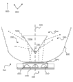
Fig. 1 is the schematic diagram in cross section that is arranged in the embodiment of the photoconduction of the present invention in the embodiment of light fixture of the present invention.
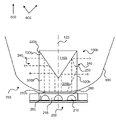
Fig. 2 is the schematic diagram in cross section that is arranged in the embodiment of the photoconduction of the present invention in the embodiment of light fixture of the present invention.
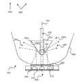
Fig. 3 is the schematic diagram in cross section that is arranged in the embodiment of the photoconduction of the present invention in the embodiment of light fixture of the present invention.
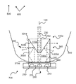
Fig. 4 is the schematic diagram in cross section that is arranged in the embodiment of the photoconduction of the present invention in the embodiment of light fixture of the present invention.
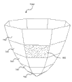
Fig. 5 is the schematic diagram of perspective view of the embodiment of photoconduction of the present invention.
The specific embodiment
Fig. 1-4th, is arranged in the schematic diagram in cross section of the embodiment of the photoconduction of the present invention in the embodiment of light fixture of the present invention.First, will jointly with reference to Fig. 1-4, common characteristic be described.Secondly, difference will be described.When reference example is during as all embodiment of photoconduction, by the general reference of using such as 100.When with reference to specific embodiment, refering in particular to such as for example 100bd will be used.
The light fixture 700 that comprises photoconduction 100, light source 200 and reflector 800 is disclosed.Reflector 800 is applicable to the light source of the group selection from high-intensity discharge lamp and Halogen lamp LED.Therefore, reflector 800 may manufacture at first for using together with high-intensity discharge lamp or Halogen lamp LED, but due to photoconduction 100, reflector 800 can be used by the light source 200 together with the form with at least one light emitting diode 210.
Photoconduction 100 has and has the conus portion of cone shape 110.The central axis 120 of conus portion 110 is on first direction 500.
Light from light source 200 distributes and penetrates with hemispherical, and it is orientated on first direction 500.Photoconduction 100 is arranged to along the major part of second direction 600 guiding light 240, and wherein, first direction 500 is not equal to second direction 600.It should be noted, second direction 600 is broadly explained in this article.Second direction 600 can be any direction that is not parallel to first direction 500.
Conus portion 110 has circumferential surface 130.Light from light source 200 is arranged to reflection on the circumferential surface 130 at conus portion 110, makes after reflection, and light is directed along second direction 600.
Circumferential surface 130 can comprise reflectance coating.Reflectance coating can be from least one in mirror-reflection and irreflexive group.Reflectance coating can be any type known to the skilled, for example, and metal coating.
Circumferential surface 130 can be at least one from group segmentation and minute face.This will be interpreted as, and circumferential surface can be embodied as to have and comprises that scope is from the various embodiment of 0 to unlimited minute face and/or segmentation amount.Divide face to distribute along segmentation.Alternatively, divide face to distribute randomly.Divide face and/or segmentation to can be smooth.Alternatively, divide face and/or segmentation can there is corrugated surface.
Fig. 5 discloses the embodiment of photoconduction.Need to understand, the feature of photoconduction 100e is also applicable to photoconduction 100abcd.The circumferential surface of photoconduction 100e comprises minute face and segmentation.Divide face 140 to form segmentations.Divide face 160 to there is corrugated surface.It should be noted, but photoconduction can be embodied as and has minute face there is no a segmentation.
As discussed previously, the photoconduction 100ac in Fig. 1 and Fig. 3 has conus portion 110ac.These conus portions 110ac can for example be attached to reflector 800 or be attached to the housing (not shown) of light fixture 700.Can use and known to those skilled in the art optical element is assemblied in to the method before light source.Such as, can use steel bracket.
The photoconduction 100cd of Fig. 3-4 is included in the pass through openings 140cd at the central part place of conus portion 110cd, makes to continue along first direction 500 through conus portion 110cd from the light of center light source 200, that be directed to conus portion 110cd.Therefore, photoconduction 100cd is arranged to along the less important part of first direction 500 guiding light 230.
In Fig. 2 and Fig. 4, photoconduction 100bd comprises the barrel portion 300bd of cylindrical shape.Preferably, barrel portion 300bd provides total internal reflection.Total internal reflection is reflected the light that is interpreted as internally reflecting in barrel portion 300bd individually due to the difference in the refractive index between photoconduction and surrounding air, causes loss-free reflection.Base portion 310bd from the light of light source 200 by barrel portion 300bd enters photoconduction 100bd.Along approaching the light being incident on sidewall 320bd in the direction of surface normal, towards reflector 800, continue across sidewall 320bd.With respect to surface normal, with wide-angle, be incident on light on sidewall 320bd and be reflected (for example, referring to,, light 250).Incidence angle with respect to surface normal is larger, and more light is reflected.
The height that arrives reflector 800 from the light of photoconduction 100 is determined by the height of conus portion 110.This can be by changing the appended height of receiving of barrel portion 110ac or changing by changing the height of barrel portion 300bd.
The angle that light sends from photoconduction 100ac is decided by the drift angle 135 of conus portion 110ac.
Put it briefly, the disclosed embodiments relate to a kind of photoconduction 100a and comprise the light fixture 700 of such photoconduction 100a.The light of photoconduction 100a guiding along first direction 500 from comprising that the light source 200 of at least one light emitting diode 210 sends.Photoconduction 100 is along the major part of second direction 600 guiding light, and wherein, first direction 500 is not equal to second direction 600.Photoconduction 100a comprises the conus portion 110a with cone shape, and the central axis 120 of conus portion 110a is on first direction 500.Photoconduction 100a can be used for the reflector 800 using together with high-intensity discharge lamp or Halogen lamp LED together with initial manufactured, but because this photoconduction 100a, this reflector 800 can use together with the light source 200 of the form with at least one light emitting diode 210.
Although explain and described the present invention in accompanying drawing and description above, such explanation and describe should be counted as illustrative or exemplary rather than restrictive; The invention is not restricted to the disclosed embodiments.
Those skilled in the art, when implementing invention required for protection, by the claim of studying accompanying drawing, disclosure and enclosing, can understand and implement other modification of disclosed embodiment.In the claims, word " comprises " does not get rid of other element or step, and indefinite article " " or " one " do not get rid of a plurality of.Single processor or other unit can meet the function of some of recording in claim.The pure fact of recording certain measures in mutually different dependent claims does not show that the combination of these measures can not advantageously be used.Any reference marker in the claims should not be interpreted as the restriction to scope.
Claims (13)
- One kind for guiding along first direction (500) from comprising the photoconduction (100) of the light that the light source (200) of at least one light emitting diode (210) sends,Wherein, described photoconduction (100) is arranged to guide along second direction (600) major part of described light, and wherein, described first direction (500) is not equal to described second direction (600),Wherein, described photoconduction (100) comprises the conus portion (110) with cone shape, wherein, the central axis (120) of described conus portion (110) is on described first direction (500), and wherein, described conus portion (110) has circumferential surface (130).
- 2. photoconduction according to claim 1 (100), wherein, light from described light source (200) is arranged to be reflected on the circumferential surface (130) in described conus portion (110), makes after reflection, and described light is directed along described second direction (600).
- 3. according to the photoconduction (100) described in any one in claim 1-2, wherein, described circumferential surface (130) comprises reflectance coating.
- 4. photoconduction according to claim 3 (100), wherein, described reflectance coating is from least one in mirror-reflection and irreflexive group.
- 5. according to the photoconduction (100e) described in any one in claim 1-4, wherein, described circumferential surface (130) is from least one in the group of segmentation and minute face.
- 6. according to the photoconduction (100) described in any one in claim 1-5, wherein, described photoconduction (100cd) is arranged to guide along described first direction (500) the less important part of described light (230).
- 7. according to the photoconduction (100) described in any one in claim 1-6, wherein, the center of described conus portion (110cd) comprises pass through openings (140cd), makes to continue along described first direction (500) through described conus portion (110cd) from the light at center described light source (200), that be directed to described conus portion (110cd).
- 8. according to the photoconduction (100) described in any one in claim 1-7, wherein, described conus portion (110bd) is arranged in the barrel portion (300bd) of cylindrical shape.
- 9. photoconduction according to claim 8 (100), wherein, described barrel portion (30bd) be arranged to provide total internal reflection.
- 10. one kind comprises according to the light fixture (700) of the photoconduction (100) described in any one in claim 1-9.
- 11. light fixtures according to claim 10 (700), further comprise light source (200), and described light source (200) comprises at least one light emitting diode (200).
- 12. light fixtures according to claim 11 (700), wherein, described light source further comprises at least one in blending bin (250) and diffusion outgoing window (260).
- 13. according to the light fixture (700) described in any one in claim 10-12, further comprises reflector (800), and wherein, described reflector (800) is applicable to from the light source of the group selection of high-intensity discharge lamp and Halogen lamp LED.
Applications Claiming Priority (3)
| Application Number | Priority Date | Filing Date | Title |
|---|---|---|---|
| EP11172400 | 2011-07-01 | ||
| EP11172400.1 | 2011-07-01 | ||
| PCT/IB2012/053273 WO2013005142A1 (en) | 2011-07-01 | 2012-06-28 | Light guide |
Publications (1)
| Publication Number | Publication Date |
|---|---|
| CN103649630A true CN103649630A (en) | 2014-03-19 |
Family
ID=46604012
Family Applications (1)
| Application Number | Title | Priority Date | Filing Date |
|---|---|---|---|
| CN201280032815.7A Pending CN103649630A (en) | 2011-07-01 | 2012-06-28 | Light guide |
Country Status (5)
| Country | Link |
|---|---|
| US (1) | US20140126216A1 (en) |
| EP (1) | EP2726781B1 (en) |
| JP (1) | JP6118317B2 (en) |
| CN (1) | CN103649630A (en) |
| WO (1) | WO2013005142A1 (en) |
Cited By (1)
| Publication number | Priority date | Publication date | Assignee | Title |
|---|---|---|---|---|
| CN104976555A (en) * | 2014-12-31 | 2015-10-14 | 苏州东善微光光电技术有限公司 | Lighting device and method for plants |
Families Citing this family (6)
| Publication number | Priority date | Publication date | Assignee | Title |
|---|---|---|---|---|
| EP3014327A1 (en) * | 2013-06-27 | 2016-05-04 | Koninklijke Philips N.V. | Lighting device |
| CN104344351A (en) * | 2013-07-23 | 2015-02-11 | 富优技研股份有限公司 | Manufacturing method for light guide column |
| US9279548B1 (en) | 2014-08-18 | 2016-03-08 | 3M Innovative Properties Company | Light collimating assembly with dual horns |
| JP6475953B2 (en) * | 2014-11-10 | 2019-02-27 | スタンレー電気株式会社 | Lighting device |
| JP6563772B2 (en) * | 2015-10-20 | 2019-08-21 | 信号電材株式会社 | lighting equipment |
| DE102016204697A1 (en) * | 2016-03-22 | 2017-09-28 | Osram Gmbh | Retrofit lamp and vehicle headlight with retrofit lamp |
Citations (5)
| Publication number | Priority date | Publication date | Assignee | Title |
|---|---|---|---|---|
| FR2639683A1 (en) * | 1988-11-28 | 1990-06-01 | Autorupteur Cie Nle | Light projector |
| US6558032B2 (en) * | 2000-08-25 | 2003-05-06 | Stanley Electric Co., Ltd. | LED lighting equipment for vehicle |
| US6758582B1 (en) * | 2003-03-19 | 2004-07-06 | Elumina Technology Incorporation | LED lighting device |
| CN101310142A (en) * | 2005-11-17 | 2008-11-19 | 皇家飞利浦电子股份有限公司 | Lamp assembly |
| US20100254128A1 (en) * | 2009-04-06 | 2010-10-07 | Cree Led Lighting Solutions, Inc. | Reflector system for lighting device |
Family Cites Families (12)
| Publication number | Priority date | Publication date | Assignee | Title |
|---|---|---|---|---|
| DE2133719C3 (en) * | 1971-07-07 | 1978-08-24 | Original Hanau Quarzlampen Gmbh, 6450 Hanau | Operating light |
| US4037096A (en) * | 1974-08-09 | 1977-07-19 | American Sterilizer Company | Illuminator apparatus using optical reflective methods |
| US5535111A (en) * | 1994-04-29 | 1996-07-09 | Thomas & Betts Corporation | Quartz halogen flood light assembly having improved lamp and reflector |
| TWI240788B (en) * | 2000-05-04 | 2005-10-01 | Koninkl Philips Electronics Nv | Illumination system, light mixing chamber and display device |
| JP4816707B2 (en) * | 2002-03-20 | 2011-11-16 | 豊田合成株式会社 | Light emitter and automobile backlight |
| FR2846400B1 (en) * | 2002-10-28 | 2005-10-07 | Valeo Vision | SIGNALING LIGHT COMPRISING A DEVICE FOR RECOVERING AND DISTRIBUTING THE LUMINOUS FLOW TO AN ANNULAR REFLECTOR |
| US7607808B2 (en) * | 2004-06-16 | 2009-10-27 | Continental Automotive Systems Us, Inc. | Instrument panel housing with light diffuser |
| KR100534590B1 (en) * | 2005-05-26 | 2005-12-08 | 서종범 | Input device and position recognition method using ultrasound |
| JP2007317431A (en) * | 2006-05-24 | 2007-12-06 | Ushio Inc | Lighting system |
| US9086213B2 (en) * | 2007-10-17 | 2015-07-21 | Xicato, Inc. | Illumination device with light emitting diodes |
| JP5022860B2 (en) * | 2007-10-23 | 2012-09-12 | パナソニック株式会社 | Lighting device for production |
| US7922366B2 (en) * | 2008-11-07 | 2011-04-12 | Chia-Mao Li | LED light source with light refractor and reflector |
-
2012
- 2012-06-28 US US14/129,360 patent/US20140126216A1/en not_active Abandoned
- 2012-06-28 CN CN201280032815.7A patent/CN103649630A/en active Pending
- 2012-06-28 WO PCT/IB2012/053273 patent/WO2013005142A1/en active Application Filing
- 2012-06-28 EP EP12742952.0A patent/EP2726781B1/en active Active
- 2012-06-28 JP JP2014518028A patent/JP6118317B2/en active Active
Patent Citations (5)
| Publication number | Priority date | Publication date | Assignee | Title |
|---|---|---|---|---|
| FR2639683A1 (en) * | 1988-11-28 | 1990-06-01 | Autorupteur Cie Nle | Light projector |
| US6558032B2 (en) * | 2000-08-25 | 2003-05-06 | Stanley Electric Co., Ltd. | LED lighting equipment for vehicle |
| US6758582B1 (en) * | 2003-03-19 | 2004-07-06 | Elumina Technology Incorporation | LED lighting device |
| CN101310142A (en) * | 2005-11-17 | 2008-11-19 | 皇家飞利浦电子股份有限公司 | Lamp assembly |
| US20100254128A1 (en) * | 2009-04-06 | 2010-10-07 | Cree Led Lighting Solutions, Inc. | Reflector system for lighting device |
Cited By (1)
| Publication number | Priority date | Publication date | Assignee | Title |
|---|---|---|---|---|
| CN104976555A (en) * | 2014-12-31 | 2015-10-14 | 苏州东善微光光电技术有限公司 | Lighting device and method for plants |
Also Published As
| Publication number | Publication date |
|---|---|
| JP2014527258A (en) | 2014-10-09 |
| US20140126216A1 (en) | 2014-05-08 |
| WO2013005142A1 (en) | 2013-01-10 |
| JP6118317B2 (en) | 2017-04-19 |
| EP2726781A1 (en) | 2014-05-07 |
| EP2726781B1 (en) | 2019-08-07 |
Similar Documents
| Publication | Publication Date | Title |
|---|---|---|
| EP2844915B1 (en) | Reflector and lamp comprised thereof | |
| CN103649630A (en) | Light guide | |
| JP5615516B2 (en) | Rear-mounted light-emitting diode module for automotive rear combination lamps | |
| US20200224856A1 (en) | Downwardly directing spatial lighting system | |
| EP1811225B1 (en) | Lens for LED lamps | |
| JP2010192439A (en) | Light emitting device and light guide member for the same | |
| JP6072785B2 (en) | Optical waveguide | |
| US8403538B2 (en) | Color homogenizing optical assembly | |
| CA2862702A1 (en) | Optical system and lighting device comprised thereof | |
| US8956015B2 (en) | Light-emitting apparatus and lighting system | |
| US20140078730A1 (en) | Lamp system having parabolic reflector with two reflections for recycling light | |
| CN219473486U (en) | Intelligent lamp | |
| JP5950198B2 (en) | lighting equipment | |
| KR102134962B1 (en) | Preventing color sepatation multiple array light device | |
| CN103104884A (en) | Secondary optical device for annular light-emitting diode array | |
| JP5676822B2 (en) | Street lamp lighting device | |
| CN205065402U (en) | Wide -angle light -emitting diode (LED) lamp | |
| CN105202389B (en) | Big-angle LED lamp | |
| KR20190049457A (en) | An led lamp and a lighting device including the same | |
| KR101083431B1 (en) | Lighting apparatus for street lamp | |
| CN104718467A (en) | Lighting device for indirect illumination having prism elements | |
| KR20090094718A (en) | Asymmetric indirect lighting collimator |
Legal Events
| Date | Code | Title | Description |
|---|---|---|---|
| PB01 | Publication | ||
| PB01 | Publication | ||
| C10 | Entry into substantive examination | ||
| SE01 | Entry into force of request for substantive examination | ||
| TA01 | Transfer of patent application right |
Effective date of registration: 20170320 Address after: Eindhoven Applicant after: KONINKL PHILIPS N.V. Address before: Holland Ian Deho Finn Applicant before: Koninkl Philips Electronics NV |
|
| TA01 | Transfer of patent application right | ||
| RJ01 | Rejection of invention patent application after publication |
Application publication date: 20140319 |
|
| RJ01 | Rejection of invention patent application after publication |
