CN102741452A - Chemical vapor deposition coating, article, and method - Google Patents
Chemical vapor deposition coating, article, and method Download PDFInfo
- Publication number
- CN102741452A CN102741452A CN2010800498267A CN201080049826A CN102741452A CN 102741452 A CN102741452 A CN 102741452A CN 2010800498267 A CN2010800498267 A CN 2010800498267A CN 201080049826 A CN201080049826 A CN 201080049826A CN 102741452 A CN102741452 A CN 102741452A
- Authority
- CN
- China
- Prior art keywords
- layer
- coating
- functionalized
- oxidation
- dimethylsilane
- Prior art date
- Legal status (The legal status is an assumption and is not a legal conclusion. Google has not performed a legal analysis and makes no representation as to the accuracy of the status listed.)
- Pending
Links
Images


Classifications
-
- C—CHEMISTRY; METALLURGY
- C23—COATING METALLIC MATERIAL; COATING MATERIAL WITH METALLIC MATERIAL; CHEMICAL SURFACE TREATMENT; DIFFUSION TREATMENT OF METALLIC MATERIAL; COATING BY VACUUM EVAPORATION, BY SPUTTERING, BY ION IMPLANTATION OR BY CHEMICAL VAPOUR DEPOSITION, IN GENERAL; INHIBITING CORROSION OF METALLIC MATERIAL OR INCRUSTATION IN GENERAL
- C23C—COATING METALLIC MATERIAL; COATING MATERIAL WITH METALLIC MATERIAL; SURFACE TREATMENT OF METALLIC MATERIAL BY DIFFUSION INTO THE SURFACE, BY CHEMICAL CONVERSION OR SUBSTITUTION; COATING BY VACUUM EVAPORATION, BY SPUTTERING, BY ION IMPLANTATION OR BY CHEMICAL VAPOUR DEPOSITION, IN GENERAL
- C23C16/00—Chemical coating by decomposition of gaseous compounds, without leaving reaction products of surface material in the coating, i.e. chemical vapour deposition [CVD] processes
- C23C16/22—Chemical coating by decomposition of gaseous compounds, without leaving reaction products of surface material in the coating, i.e. chemical vapour deposition [CVD] processes characterised by the deposition of inorganic material, other than metallic material
- C23C16/30—Deposition of compounds, mixtures or solid solutions, e.g. borides, carbides, nitrides
- C23C16/32—Carbides
- C23C16/325—Silicon carbide
-
- B—PERFORMING OPERATIONS; TRANSPORTING
- B05—SPRAYING OR ATOMISING IN GENERAL; APPLYING FLUENT MATERIALS TO SURFACES, IN GENERAL
- B05D—PROCESSES FOR APPLYING FLUENT MATERIALS TO SURFACES, IN GENERAL
- B05D1/00—Processes for applying liquids or other fluent materials
- B05D1/60—Deposition of organic layers from vapour phase
-
- C—CHEMISTRY; METALLURGY
- C23—COATING METALLIC MATERIAL; COATING MATERIAL WITH METALLIC MATERIAL; CHEMICAL SURFACE TREATMENT; DIFFUSION TREATMENT OF METALLIC MATERIAL; COATING BY VACUUM EVAPORATION, BY SPUTTERING, BY ION IMPLANTATION OR BY CHEMICAL VAPOUR DEPOSITION, IN GENERAL; INHIBITING CORROSION OF METALLIC MATERIAL OR INCRUSTATION IN GENERAL
- C23C—COATING METALLIC MATERIAL; COATING MATERIAL WITH METALLIC MATERIAL; SURFACE TREATMENT OF METALLIC MATERIAL BY DIFFUSION INTO THE SURFACE, BY CHEMICAL CONVERSION OR SUBSTITUTION; COATING BY VACUUM EVAPORATION, BY SPUTTERING, BY ION IMPLANTATION OR BY CHEMICAL VAPOUR DEPOSITION, IN GENERAL
- C23C16/00—Chemical coating by decomposition of gaseous compounds, without leaving reaction products of surface material in the coating, i.e. chemical vapour deposition [CVD] processes
- C23C16/56—After-treatment
-
- C—CHEMISTRY; METALLURGY
- C23—COATING METALLIC MATERIAL; COATING MATERIAL WITH METALLIC MATERIAL; CHEMICAL SURFACE TREATMENT; DIFFUSION TREATMENT OF METALLIC MATERIAL; COATING BY VACUUM EVAPORATION, BY SPUTTERING, BY ION IMPLANTATION OR BY CHEMICAL VAPOUR DEPOSITION, IN GENERAL; INHIBITING CORROSION OF METALLIC MATERIAL OR INCRUSTATION IN GENERAL
- C23C—COATING METALLIC MATERIAL; COATING MATERIAL WITH METALLIC MATERIAL; SURFACE TREATMENT OF METALLIC MATERIAL BY DIFFUSION INTO THE SURFACE, BY CHEMICAL CONVERSION OR SUBSTITUTION; COATING BY VACUUM EVAPORATION, BY SPUTTERING, BY ION IMPLANTATION OR BY CHEMICAL VAPOUR DEPOSITION, IN GENERAL
- C23C8/00—Solid state diffusion of only non-metal elements into metallic material surfaces; Chemical surface treatment of metallic material by reaction of the surface with a reactive gas, leaving reaction products of surface material in the coating, e.g. conversion coatings, passivation of metals
- C23C8/06—Solid state diffusion of only non-metal elements into metallic material surfaces; Chemical surface treatment of metallic material by reaction of the surface with a reactive gas, leaving reaction products of surface material in the coating, e.g. conversion coatings, passivation of metals using gases
- C23C8/08—Solid state diffusion of only non-metal elements into metallic material surfaces; Chemical surface treatment of metallic material by reaction of the surface with a reactive gas, leaving reaction products of surface material in the coating, e.g. conversion coatings, passivation of metals using gases only one element being applied
- C23C8/10—Oxidising
-
- H—ELECTRICITY
- H01—ELECTRIC ELEMENTS
- H01L—SEMICONDUCTOR DEVICES NOT COVERED BY CLASS H10
- H01L21/00—Processes or apparatus adapted for the manufacture or treatment of semiconductor or solid state devices or of parts thereof
- H01L21/02—Manufacture or treatment of semiconductor devices or of parts thereof
- H01L21/02104—Forming layers
- H01L21/02365—Forming inorganic semiconducting materials on a substrate
- H01L21/02612—Formation types
- H01L21/02617—Deposition types
- H01L21/0262—Reduction or decomposition of gaseous compounds, e.g. CVD
-
- B—PERFORMING OPERATIONS; TRANSPORTING
- B05—SPRAYING OR ATOMISING IN GENERAL; APPLYING FLUENT MATERIALS TO SURFACES, IN GENERAL
- B05D—PROCESSES FOR APPLYING FLUENT MATERIALS TO SURFACES, IN GENERAL
- B05D2202/00—Metallic substrate
- B05D2202/10—Metallic substrate based on Fe
- B05D2202/15—Stainless steel
-
- Y—GENERAL TAGGING OF NEW TECHNOLOGICAL DEVELOPMENTS; GENERAL TAGGING OF CROSS-SECTIONAL TECHNOLOGIES SPANNING OVER SEVERAL SECTIONS OF THE IPC; TECHNICAL SUBJECTS COVERED BY FORMER USPC CROSS-REFERENCE ART COLLECTIONS [XRACs] AND DIGESTS
- Y10—TECHNICAL SUBJECTS COVERED BY FORMER USPC
- Y10T—TECHNICAL SUBJECTS COVERED BY FORMER US CLASSIFICATION
- Y10T428/00—Stock material or miscellaneous articles
- Y10T428/24—Structurally defined web or sheet [e.g., overall dimension, etc.]
- Y10T428/24802—Discontinuous or differential coating, impregnation or bond [e.g., artwork, printing, retouched photograph, etc.]
Abstract
The present invention relates to a chemical vapor deposition coating, a chemical vapor deposition article, and a chemical vapor deposition method. The coating, article, and method involve thermal decomposition of dimethylsilane to achieve desired surface properties.
Description
Right of priority
The application requires to submit on October 27th, 2009 and is entitled as the U.S. Provisional Patent Application number 61/255 of " DIMETHYLSILANE CHEMICAL VAPOR DEPOSITION COATING AND COATING PROCESS (dimethylsilane chemical vapor deposited coatings and coating process) "; Submitted and be entitled as the U.S. Provisional Patent Application number 61/267 of " OXIDIZED VAPOR DEPOSITION COATING AND COATING PROCESS (oxidation vapour deposition coating and coating process) " on December 7th, 237 and 2009; 228 right of priority and rights and interests, these two provisional application are attached among this paper through quoting in full.
Invention field
The disclosure relates to chemical vapour deposition.More specifically, the disclosure relates to the chemical vapour deposition on base material owing to the decomposition of dimethylsilane.
Background of invention
Usually, the surface of base material does not comprise the performance characteristic of expectation.The performance characteristic that can not comprise specific expectation can cause in some environment surface deterioration, can not satisfy some performance requriements or their combination.For example, in some environment, the surfactivity that metal, glass and ceramic surface can stand not expect, for example chemisorption, catalytic activity, corrodibility invasion and attack, oxidation, by product gathering or stiction and/or other surfactivitys of not expecting.
The surfactivity of not expecting can cause the chemisorption of other molecules, reversible and irreversible physical adsorption, the catalyzed reaction property with other molecules, the invasion and attack from exotic class (specy), the molecular breakdown on surface or their combination of other molecules.
But the surfactivity of applying coatings to protect the surface to avoid not expecting.A kind of known method of deposited coatings is chemical vapour deposition from the teeth outwards.Chemical vapour deposition makes solid material deposition preset time to form coating by steam under controlled atmosphere and temperature condition.Chemical vapour deposition can comprise primary treatment, and then functionalized (surface reaction) is to add predetermined molecule.
For the performance characteristic of some expectation is provided, but the deposited amorphous silicon hydride is surperficial, and can with the unsaturated hydrocarbons reagent react so that the surface-treated of base material.Yet, to responsive, limit their application thus by the high pH medium dissolves of causticity based on the chemical vapour deposition material of non-crystalline silicon.These materials are not wear-resisting or enough hard to be effective to have the environment of impact or skimming wear.In addition, use functionalized common the need use metal catalyst of unsaturated hydrocarbons to silicon materials.The existence that these methods suffer to remove common difficulty of this catalyzer and catalyzer fully from treated system can be introduced the surface-active shortcoming of not expecting once more.
The molecule that comprises silicon, carbon and hydrogen was thought in the past and is not expected as chemical vapor deposition precursor or in the presence of other sedimentary energy (for example plasma body and microwave field), combine to use with other chemical vapor deposition precursor.Therefore, through the thermal chemical vapor deposition technology, do not recognize the character relevant in the past with these molecules.
What need is coating, goods and the method that does not suffer the prior art shortcoming.
Summary of the invention
An exemplary comprises the thermal chemical vapor deposition coating.Said thermal chemical vapor deposition coating comprises the thermolysis of dimethylsilane.
Another exemplary comprises the thermal chemical vapor deposition method.Said method be included in the CVD chamber preparation base material and in CVD chamber the thermolysis dimethylsilane to form coating.
Another exemplary comprises chemical vapour deposition prepn (article).Said goods comprise surface and the layer that on the surface of goods, forms through the thermolysis of dimethylsilane in CVD chamber.Said layer comprises first part and the second section that is limited sedimentary molecule on this layer.The said molecule that limits first part and second section comprises the molecule fragment that contains H, C and Si.
An advantage of embodiment is and can former unavailable molecule of silicon, carbon and hydrogen that comprises be applied to substrate surface.
Another advantage of embodiment is need not other decomposition energy (for example plasma body and microwave energy) can carry out thermal chemical vapor deposition, to help the decomposition of dimethylsilane.
Another advantage of embodiment is that said silicon, carbon and hydrogen material are insensitive to dissolving in high pH medium.
Another advantage of embodiment is that the material of oxidation shows improved wear resistance and hardness, is used to have impact or the improved application of the environment of skimming wear.
Another advantage of embodiment is in formation comprises the coating of silicon, carbon and hydrogen, can avoid the use of the additional metals catalyzer.
Another advantage of embodiment is to reduce or eliminate remaining catalyst activity.
Another advantage of embodiment is to eliminate the step that is used to remove catalyzer.
Another advantage of embodiment is for using the nonflammable material that can improve security.
Herein disclosed is other aspects of embodiment of the present invention.By following accompanying drawing and detailed description, those skilled in the art will be familiar with and understand other feature and advantage of characteristic discussed above and the application.
Embodiment 1
First embodiment is included under the 8p.si.a. gas, under 450 ℃, introduces dimethylsilane 2 hours to base material 100, with form layers 102.In first embodiment, almost can not detect (that is, being very difficult to visually discover) on bright finished 316 stainless steel samples (flavescence a little) upper strata 102.Measurement is presented at that the water contact angle data are about 60 ° before the depositing treatment.After with the dimethylsilane depositing treatment, contact angle is increased to about 102 °.Though layer 102 cannot see, data declaration has the deposition as thin as a wafer of the carbon silyl material of remarkable density on the layer 102 on surface 105.Because the not enough sensitivities of available spectroscopic techniques detect coating, estimate that the thickness of layer 102 is about 100 dusts.
Embodiment 2
Second embodiment is included under the 8p.s.i.a. gas, under 450 ℃, introduces dimethylsilane 15 hours to base material 100, with form layers 102.In a second embodiment, layer 102 colorful Visible Luminescence rainbow are arranged.For 316 stainless steel surface of minute surface ornamenting and the silicon wafer surface of polishing, measuring the average deionized water contact angle data of demonstration is about 100 °.The FT-IR demonstration is based on 2950cm
-1Reading have C-H, be based on 792cm
-1Reading have Si-C and be based on 2102cm
-1Reading have the Si-H part.Thickness through spectrophotometric determination layer 102 is about 800 dusts.Also utilize other measurements of Auger electron spectrum.Measurement is presented at the concentration raising of Si and C atom on the layer 102.Measure the concentration reduction that further shows Si and C atom when arriving spreading area 108, illustrated like the concentration raising of Fe, Cr and Ni atom.When arrival exceeded the point of spreading area 108, it was progressive to zero to measure the concentration that shows Si and C atom.Measure and to show that also spreading area 108 can improve based on the concentration of O atom and discern (before deposition, the result of the oxide on surface on the surface 105 of base material 100).
The 3rd embodiment is included under the 8p.s.i.a. gas, under 450 ℃, introduces dimethylsilane 15 hours to base material 100; With form layers 102, subsequently under about 100-200p.s.i.a. gas, under 450 ℃; Make water; In rare gas element, with layer 102 oxidation 2 hours of base material 100, to form the layer 802 of oxidation.The FT-IR data can not disclose any functional moiety (Si-OH or Si-H) that remarkable existence is used for the surface-treated chemistry.Resulting carboxyl silane material discloses and compares with natural carbon silane, and hardness and wear resistance are improved.The contact angle of layer 802 on the Si wafer of oxidation is 86.6 °, and improves the existence of Si-O-Si group.
Embodiment 4
The 4th embodiment is included under the 8p.s.i.a. gas, under 450 ℃, introduces dimethylsilane 15 hours to base material 100; With form layers 102; Under about 100-200p.s.i.a. gas, under 300 ℃, use the oxidising agent mixture subsequently; With layer 102 oxidation 2 hours of base material 100, to form the layer 805 of oxidation.This oxidising agent mixture comprises the sky G&W.According to the FT-IR data, the layer 805C-H group of oxidation reduces (comparing with embodiment 3), and the Si-C group reduces (comparing with embodiment 3) and the Si-OH group improves (comparing with embodiment 3).
Embodiment 5
The 5th embodiment is included under the 8p.si.a. gas, under 450 ℃, introduces dimethylsilane 15 hours to base material 100; With form layers 102; Under about 100-200p.si.a. gas, under 300 ℃, use air subsequently; Layer 102 oxidation that will be on base material 100 2 hours are to form the layer 805 of oxidation.The 5th embodiment produces the carbon silane material of oxidation, in the FT-IR data, observes significant Si-OH and stretches (wide; 3414cm
-1).For deionized water, contact angle is through being measured as 50.9 °.The electrochemical impedance power spectrum shows the low frequency impedance Z
Lf=about 7.27kohm.Use the wear resistance of tribometer (CSM Instruments S/N 18-343) analysis of material, use 0.5N power via standard 100Cr6 ball, round wire speed is 3.00cm/s, shows 4.141e thus
-03Wearing and tearing (mm
3/ N m).The layer 805 of oxidation has lower friction (comparing with embodiment 3), higher wear resistance (comparing with embodiment 3) and has the Si-O-Si group.
Embodiment 6
The 6th embodiment comprises that the layer 102 that uses ethene in embodiment 2, to form is functionalized, to form functionalized layer 110.The water contact angle of functionalized layer 110 be 98.3 ° forward with 85.1 ° backward.Shown in figure 10, (be based on 1027cm based on lacking the Si-O-Si group
-1Stretching) and the Si-H group amount that reduces (be based on 2091cm
-1Stretching), FT-IR data presentation seldom oxidation takes place.
Embodiment 7
The 7th embodiment comprises that the layer 102 that uses ethene in embodiment 2, to form is functionalized, to form functionalized layer 110.Then, through 5ml deionized water (DI) is joined in the chamber, make functionalized layer 110 oxidation.The chamber is exposed to some nitrogen washes and gentle vacuum, from the container of sealing, to remove air.Temperature in the chamber kept about 2 hours down at 450 ℃, was back to room temperature subsequently.Functionalized layer 110 oxidation are formed functionalized layer 804 with rear oxidation.Functionalized layer 804 water contact angle data with rear oxidation be 95.6 ° forward with 65.9 ° backward.Compare with the functionalized layer 110 that in embodiment 6, forms, shown in figure 10, FT-IR shows that the amount of oxidation raising Si-O-Si group (is based on 1027cm
-1Stretching) and the amount that reduces the Si-H group (be based on 2091cm
-1Stretching).
Though shown and described only some characteristic and embodiment of the present invention; But those skilled in the art (for example can expect many modifications and variation; The size of each element, size, structure, shape and ratio; Parameter value (for example, temperature, pressure etc.), install to arrange, the use of material, color, orientation etc.), and do not depart from the new instruction and the advantage of theme described in the claim in itself.The order of any process or method steps or order can change or rearrangement according to alternate embodiment.Therefore, it should be understood that accompanying claims is intended to contain all these modifications and the variation that falls in the true spirit scope of the present invention.In addition, when attempting the concise and to the point description of exemplary is provided, all characteristics (that is, with irrelevant those of the best mode of the embodiment of the present invention of present expection, or making irrelevant those of the invention mandate of asking for protection) of actual execution possibly not described.It should be understood that when the execution of exploitation any of these reality,, can carry out numerous carrying out specific decision as in any engineering or design item.Such development effort possibly be complicated and consuming time, but still is the normal work to do of design, making and the manufacturing of benefiting from those of ordinary skill of the present disclosure, and need not undo experimentation.
The accompanying drawing summary
Fig. 1 shows an exemplary according to the carbon silane coating of the disclosure on base material.
Fig. 2 shows the Auger electron spectrum figure of an exemplary that on base material, has the carbon silane coating of layer according to the disclosure.
Fig. 3 shows an exemplary according to the functionalized carbon silane coating of the disclosure on base material.
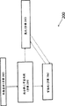
Fig. 4 shows the chemical gaseous phase depositing process according to an exemplary of the present disclosure.
Fig. 5 is presented at according to a kind of exemplary process method in the chemical gaseous phase depositing process of the present disclosure.
Fig. 6 is presented at according to a kind of exemplary hot in the chemical gaseous phase depositing process of the present disclosure and decomposes.
Fig. 7 is presented at according to a kind of exemplary functionalisation step in the chemical gaseous phase depositing process of the present disclosure.
Fig. 8 is presented at according to a kind of exemplary oxidising process in the chemical gaseous phase depositing process of an embodiment of the present disclosure.
Fig. 9 is presented at according to a kind of exemplary water oxidising process in the chemical gaseous phase depositing process of an embodiment of the present disclosure.
Figure 10 shows that sedimentary functionalized surface of dimethylsilane and the sedimentary functionalized FT-IR with the surface water oxidation of dimethylsilane scheme.
Figure 11 shows the Auger electron spectrum figure of an exemplary of coating that on base material, has the layer of water oxidation according to the disclosure.
Anywhere possible, identical Reference numeral is used to represent identical parts in whole accompanying drawing.
Detailed Description Of The Invention
The invention provides the method for chemical vapor deposited coatings, chemical vapour deposition prepn and the chemical vapour deposition of the shortcoming that does not suffer prior art.For example, the embodiment of said coating, goods and the method molecule that comprises silicon, carbon and hydrogen capable of using.In one embodiment, said method is adopted in the catalyst activity and their combination that can need not the additional metals catalyzer, lack other remnants.In one embodiment, said method improves hardness, and does not have essence to reduce the character of inertia, chemical erosion resistance and/or other expectations.The exemplary coatings that forms according to the disclosure can change functionality, inertia, flexibility, hydrophobicity, erosion resistance and/or anti-stiction performance, hardness, wear resistance or their combination.
With reference to figure 1; Base material 100 according to an exemplary can comprise the surface 105 with improved surface properties; Said improved surface properties realizes that through controlled deposition layer 102 said layer 102 is given base material 100, coating 101, goods 103 or their combination with the surface action of expectation.Coating 101 through chemical vapour deposition (for example; The decomposition of dimethylsilane is to form carbon silane), then oxidation (for example, air-oxidation is to form carboxyl silane) and/or functionalized (for example; Between hydrosilanes and unsaturated hydrocarbons, to form functionalized carboxyl silane) and form.
Through making layer 102 and/or coating 101 diffuse into the surface 105 of base material 100, the surface action of giving expectation can improve the performance on surface 105.Can layer 102 be applied to any suitable substrates.For example, base material 100 can be metal base (iron content or non-iron content), glass baseplate or ceramic base material.
In an exemplary, layer 102 thermolysis through dimethylsilane form.Through the thermolysis dimethylsilane, layer 102 comprises the molecule that can be reactive site that comprises silicon, carbon and Wasserstoffatoms.These molecules in layer 102 can comprise first part 104 and second section 106.Usually, first part 104 is not space distinguishable (for example, first part 104 is limited sedimentary molecule on layer 102 with second section 106, and the spreadable whole layer 102 of these molecules) with second section 106.In addition, use a technical term " first " and " second " be not intended to hint other differences between any order, quantity difference, size difference or two portions.On the contrary, term " first " and " second " are used to distinguish two-part molecular composition.For example, in one embodiment, first part 104 comprises silicon, and second section 106 comprises carbon.In one embodiment, first part 104 is in the same place with second section 106 any combination in whole layer 102.
Fig. 2 illustrates according to an exemplary layer 102 and/or coating 101 and diffuses into base material 100.Surface applied dimethylsilane to selecting in advance causes improved chemical resistant properties, improved inertia and improved tackiness on non-diffusion coating.Fig. 2 is corresponding to the layer 102 with carbonaceous first part 104 and the second section 106 with silicon.Particularly, Fig. 2 is presented at the composition of the layer 102 in base material 100 and/or the goods 103 through the auger electron spectrometry of layer 102.
In one embodiment, with the dimethylsilane thermolysis and as amorphous carbon silane-deposited 15 hours.In this embodiment, layer 102 extends to about 130 nanometers and comprises a part of spreading area 108, and this spreading area 108 can be based on the raising of O concentration and C and Si density loss (for example, at least four factor) identification.The scope of layer 102 can be about 0.1 micron-Yue 3.0 microns.Spreading area 108 can be about 5 nanometers-500 nanometer.In one embodiment, spreading area 108 is about 20 nanometers.Layer 102 the C that consists of about 1: 0.95: 0.12 ratio: Si: O (possibly be because ground unrest and contaminant trace species from the oxygen of a small amount of existence of the 5 nanometers-120 nanometer degree of depth).In contrast, be incorporated into the C that consists of about 2: 1 ratios of the dimethylsilane of CVD chamber: Si.We think CH
x(x=0-3) part is retained and the Si-C key is destroyed, and therefore explanation layer 102 comprises the amorphous array and/or the polycrystalline microtexture of Si-C bonding.The amorphous array provides other benefit, for example reduces crackle or peels off (for example, when tension force or compression force in 100 last times of base material) and/or improve tackiness.In one embodiment, deposit multilayer coating 101 or similar coating are used for thicker layer or the character that is used to expect.
Fig. 3 shows an exemplary with functionalized layer 110.Functionalized layer 110 (for example, has formula H through the silicon hydride part with unsaturated hydrocarbons
2C=CH-R and/or HC ≡ C-R) thermal response and forming, and comprise and the R-group of all or part of bonding of the first part 104 of layer 102.The R-group can form through any suitable organic reagent with one or more unsaturated alkyls.The R-group can pass through hydrocarbon, substituted hydrocarbon (for example, halo), carbonyl, carboxyl, ester, amine, acid amides, sulfonic acid, organometallic complex and/or epoxide and form.
Fig. 4 shows a kind of exemplary chemical gaseous phase depositing process 200 that is used to form layer 102, and it comprises preparation base material (step 202) and thermolysis dimethylsilane (step 204).Preparation base material (step 202) can carry out through any suitable treatment process.For example, with reference to figure 5, preparation base material (step 202) can be included in separation substrate in the CVD chamber (substep 208), and preheating base material (substep 210) uses rare gas element washing chamber (substep 212) and the chamber found time (substep 214).
Separation substrate (substep 208) carries out in inert atmosphere indoor.The maintenance of gas flow and/or vacuum can provide controlled atmosphere in the chamber.Temperature in the thermal source may command chamber, with from substrate surface desorption water with remove remaining pollutent (substep 210).For example, pending surface can be included in the CVD chamber, and said chamber has tubing and connects, to allow gas to flow into and to flow out CVD chamber.This chamber can comprise a plurality of controlled entrance and exits, and it is provided for providing and removes a plurality of gas streams.Vacuum can be connected with one or more outlet pipes.
The degree of cleaning that depend on base material can being lower than heating several minutes-Yue 15 hours time (substep 210) under the about 1 atmospheric pressure, prepare base material through surpassing about 100 ℃ temperature.Usually, the temperature of heating is corresponding to the character of base material 100.In one embodiment, the time is about 15 hours of about 0.5-.In another embodiment, under about 450 ℃, base material was heated about 2 hours.Under vacuum, after the preparation, can use rare gas element selectivity washing chamber (substep 212) and vacuumize (substep 214).
With reference to figure 6; The thermolysis (step 204) of dimethylsilane is included under the predetermined pressure and temperature that is enough to decompose dimethylsilane dimethylsilane is incorporated into (substep 216) in the chamber; The component of self-decomposition in the future is deposited on (substep 217) on the base material 100; During coated substrate (substep 218) preset time, with the realization preset thickness, and/or the chamber (substep 220) of purging dimethylsilane.Like USP 6,444, described in 326, this patent is attached among this paper through quoting in full, and exemplary process conditions can comprise that pressure is the about 200p.si.a of about 0.01p.si.a.-.Temperature can be about 200 ℃-600 ℃.Time durations can be about 10 minutes-Yue 24 hours.
In one embodiment, the dimethylsilane of introducing (substep 216) comprises the dimethylsilane of gaseous form.In one embodiment, under the about 100p.s.i.a. pressure of about 1.0p.s.i.a.-and about 300 ℃ of-600 ℃ of temperature, base material is exposed to about 30 minutes-Yue 24 hours time of dimethylsilane gas.In an exemplary, under about 400 ℃-Yue 500 ℃ of temperature, base material 100 was exposed to dimethylsilane gas about 15 hours.The pressure of dimethylsilane gas can be the about 40p.s.i.a. of about 5p.s.i.a.-.
Subsequently the dimethylsilane thermal dissociation is become the molecule fragment that comprises H, C, Si and their combination; And this composition is deposited on (substep 217) on the base material 100, the material that comprises silicon, carbon and hydrogen that uses the decomposition by dimethylsilane to produce thus forms coating 102 (substep 218).Can under reduced pressure or use rare gas element (for example nitrogen, helium and/or argon gas), dimethylsilane gas to be incorporated in the reaction chamber as the dividing potential drop thinner.Though be not intended to be bound by theory, we think the dimethylsilane thermolysis to form carbon silyl fragment, and it reconfigures and be bonded to substrate surface.We think comprise in resulting coating on the substrate surface and on the surface in the exposure of chamber have carbon, the amorphous carbon silane of silicon and hydrogen.Sedimentary material also diffuses into the surface 105 of base material 100, like (Fig. 2, the spreading area 108) of in the Auger electron spectrum depth curve, explaining, therefore supports the pattern with base material 100 adhesions.The chamber can be with post-purge dimethylsilane and the non-sedimentary carbon silyl fragment of volatility (substep 220).If expect thicker settled layer, change mode of deposition.This realizes through changing temperature, pressure, time or their combination.Also can use a plurality of layers through repeating step 204.
Other step can be carried out in form layers 102 backs (like what further describe with reference to Fig. 1 and 2).In one embodiment, then with layer 102 functionalized (step 206), as further describing, to form functionalized layer 110 below with reference to Fig. 7.In one embodiment, with layer 102 (for example, amorphous carbon silane) oxidation (step 205), like what further describe, to form layer 802 (for example, the amorphous carboxyl silane) of oxidation below with reference to Fig. 8.In one embodiment, with functionalized layer 110 (for example, functionalized amorphous carbon silane) oxidation, to form functionalized layer 804 (for example, functionalized amorphous carboxyl silane), like what further describe below with reference to Fig. 9 with rear oxidation.In one embodiment, the layer 802 of oxidation is functionalized.
In one embodiment, method 200 further comprises layer 102 functionalized (step 206) that make base material 100, forming functionalized layer 110, describes with reference to figure 3 is concise and to the point as above.With reference to figure 7, through with by the remaining silicon hydride partial reaction of initial carbon silane-deposited (step 204), can make base material 100 the layer 102 functionalized (step 206).On base material, deposit (step 204) afterwards at carbon silane, use inert gas purge system (it can be the purging of substep 220 or independent purge step), can reaction chamber be set at predetermined functionalized temperature (substep 232) simultaneously.Purging is removed not and substrate surface bonded gaseous carbon silane moiety and/or unreacted dimethylsilane part.Behind purging and the design temperature (substep 232), the chamber is vacuumized (substep 234).
Then, indoor, under predetermined temperature and pressure, wedding agent is incorporated into indoor (substep 236).In one embodiment, use heat as motivating force, via the silicon hydride part, binding reagents also combines with the surface reaction of carbon silyl.The wedding agent instance is ethene, propylene and substituted unsaturated organic molecule.The nubbin of silicon hydride can the heating under (for example, under about 400 ℃) and H
2C=CH-R and/or HC ≡ C-R reaction.The R-group can pass through hydrocarbon, substituted hydrocarbon (for example, halo), carbonyl, carboxyl, ester, amine, acid amides, sulfonic acid, organometallic complex and/or epoxide and form.
In one embodiment, binding agent molecule combines (substep 240) subsequently with base material.Coating can comprise the carbon-silicon covalent linkage that contains the R-group.Can change the R-group, to regulate the character on surface.For example, can change the R-group, to regulate the hydrophobicity on surface.In order to regulate the hydrophobicity on surface, the R-group can be fluorinated hydrocarbons.Fluorinated hydrocarbons can form hydrophobicity and/or oleophobic property surface.In addition or alternative, the R-group can comprise provides the organometallic substituted of catalysis or biocidal properties base.Though be not intended to be bound by theory, we think that the part of silicon hydride can be via hydrosilylation mechanism and unsaturated alkyl thermal response, with the surperficial covalent bonding of substrates coated.The coating that in reaction chamber, on the surface of all exposures, obtains comprises covalently bound R-group, and this covalently bound R-group comprises R-group and carbon, silicon and hydrogen partial.
In one embodiment, method 200 further comprises layer 102 oxidation (step 205) that make base material 100, forming the layer 802 of oxidation, describes with reference to figure 3 is concise and to the point as above.In another embodiment, with functionalized layer 110 oxidation.Through be exposed under predetermined oxidizing condition can be in layer 102 any suitable chemical species of supply response property oxygen thing class, with layer 102 oxidation.For example, this chemical species can be water, oxygen, air, Nitrous Oxide, ozone, superoxide and their combination.Generally speaking, be oxidized to the main body reaction of the main body that influences coating 101.Can or reduce indoor temperature through raising, come controlled oxidation in type and/or amount, pressure and/or other suitable process conditions of indoor exposure duration, diluents.Controlled oxidation can improve or reduce the amount and/or the degree of depth of oxidation, therefore, can improve or reduce the wear resistance and/or the hardness on surface.In one embodiment, layer 102 is exposed to water (for example, in rare gas element, under about 100-200p.s.i.a. pressure, under about 450 ℃, about 2 hours).In one embodiment, functionalized layer 110 is exposed to water (for example, in rare gas element, under about 100-200p.s.i.a. pressure, under about 450 ℃, about 2 hours).
Through controlled oxidation, oxidation improves hardness and/or the wear resistance based on the chemical gaseous phase depositing process material of carbon silane and functionalized carbon silane on ferrous metal surface, non-ferrous metal surface and/or the glass surface.In one embodiment, with reference to figure 8, layer 102 be the amorphous layer of carbon silane, with its oxidation with the amorphous layer that forms carboxyl silane as layers 802 of oxidation.In one embodiment, with reference to figure 9, functionalized layer 110 be the amorphous layer of functionalized carbon silane, with its oxidation forming the amorphous surfaces of functionalized carbon silane, with its oxidation with the amorphous surfaces that forms functionalized carboxyl silane as layers 802 of oxidation.
In one embodiment, use Nitrous Oxide (N
2O) carry out oxidation (step 205).Particularly, under heating (for example, about 450 ℃), at the pure N of essence
2Under the O pressure, in the container of the sample that contains carbon-coated silane, use N
2O.In this embodiment, oxidation (step 205) over oxidation, and over oxidation to cause contact angle be about 60 °, improve the amount of N-H, Si-OH and/or C-OH group, and cause having frangible relatively scratch-resistant.
In one embodiment, use ozone to carry out oxidation (step 205).In this embodiment, think that oxidation (step 205) reduces wear resistance, reduces chemical resistant properties, reduces scratch-resistant, reduces hardness and improves acid resistance/erosion resistance.
In one embodiment, (only) makes water form the layer 802 (for example, in about 100 ℃-Yue 600 ℃ TR, about 300 ℃-Yue 600 ℃ TR, or under about 450 ℃ temperature) of oxidation as oxidising agent.In this embodiment; Oxidation (step 205) causes the contact angle on the Si wafer to be about 86.6 °, to reduce friction (comparing with the oxidising agent that uses empty G&W), reduce wear resistance (for example, comparing with the oxidising agent that uses empty G&W) and form the Si-O-Si group.
In another embodiment, use the oxidising agent comprise the sky G&W to form the layer 802 (for example, in about 100 ℃-Yue 600 ℃ TR, about 300 ℃-Yue 600 ℃ TR, or) of oxidation in about 450 ℃ temperature.In this embodiment; Oxidation (step 205) over oxidation; And the amount of reduction C-H group (for example; With only make water and compare as oxidising agent), reduce the amount (for example, comparing as oxidising agent) of Si-C group and the amount (for example, comparing as oxidising agent) of raising Si-OH/C-OH group with only making water with only making water.
In another embodiment, (only) uses air to form the layer 802 (for example, in about 100 ℃-Yue 600 ℃ TR, about 300 ℃-Yue 600 ℃ TR, or in about 450 ℃ temperature) of oxidation.In this embodiment, oxidation (step 205) reduces friction, improves wear resistance (for example, comparing with the oxidising agent that makes water) and forms Si-O-Si and Si-OH group.
In one embodiment, layer 102 has predetermined contact angle (for example, about 98.3 ° (advancing) forward), and functionalized layer 110 has higher contact angle (for example, about 100 ° forward).In one embodiment, layer 102 has predetermined contact angle (for example, about 95.6 ° forward), and functionalized layer 804 with rear oxidation has lower contact angle (for example, about 65.9 ° (reseding)) backward.In this embodiment, oxidation (step 205) forms the Si-O-Si group, reduces the amount (for example, comparing with functionalized layer 110) of Si-H group.
In one embodiment, layer 802 has lower frictional coefficient (for example, about 0.84), and by contrast, layer 102 has high friction coefficient (for example, about 0.97).Similarly, in one embodiment, the layer 802 of oxidation has lower wear rate (for example, about 6.75E-05mm
3/ N/m), by contrast, layer 102 has higher wear rate (for example, 4.73E-04mm
3/ N/m).
The layer 802 that Figure 11 illustrates according to the oxidation of an exemplary water diffuses into base material 100 (for example, stainless steel).Particularly, Figure 11 is presented at the composition of the layer 802 of the water oxidation in base material 100, coating 101 and the goods 103 through Auger electron spectrum.As directed, explain that as follows oxidation: Si-H partly experiences oxidation and is connected with eliminating to produce Si-O-Si, and some Si-C and/or uncombined carbon thing class are eliminated also.In one embodiment, the layer 802 of oxidation extends to about 1600 dusts, and comprises the spreading area 108 of about 250 dusts, can reduce based on the concentration of C and Si and discern.The scope of the layer of water oxidation can be about 0.1 micron-Yue 3.0 microns.Spreading area 108 can be about 5 nanometers-500 nanometer.The consisting of about 1.0: 1.22: 0.91 (C: Si: O), because the zone of oxidation that on base material 100, is pre-existing in, oxygen improve of the layer 802 of water oxidation.
Claims (20)
1. a thermal chemical vapor deposition coating (101), it comprises the thermolysis of dimethylsilane.
2. the coating of claim 1 (101), the thermolysis of wherein said dimethylsilane are in layer (102), and said layer (102) comprises first part (104) and second section (106), and said first part and said second section are through the qualification of the molecule in the layer (102).
3. the coating of claim 2 (101), wherein said first part (104) comprises silicon, and said second section (106) comprises carbon.
4. the coating of claim 2 (101), wherein said layer (102) comprise the amorphous array of Si-C bonding and in the polycrystalline microtexture one or more.
5. the coating of claim 1 (101), wherein said thermolysis are in the layer (802) of oxidation, and the layer of said oxidation (802) forms through using oxidising agent to layer (102) of coating (101).
6. the coating of claim 1 (101), the layer of wherein said oxidation (802) comprises amorphous carboxyl silane.
7. the coating of claim 1 (101), wherein said thermolysis are in functionalized layer (110), and said functionalized layer (110) forms through the thermal response of silicon hydride and unsaturated hydrocarbons.
8. the coating of claim 6 (101), wherein said functionalized layer (110) comprises the R-group that is connected with unsaturated hydrocarbons, said R-group is selected from hydrocarbon, substituted hydrocarbon, carbonyl, carboxyl, ester, amine, acid amides, sulfonic acid, organometallic complex and epoxide.
9. the coating of claim 6 (101), wherein said functionalized layer (110) comprises functionalized amorphous carbon silane.
10. the coating of claim 6 (101), wherein said functionalized layer (110) comprise the effect of biocidal functional group.
11. the coating of claim 1 (101), wherein said thermolysis are in functionalized layer (804) with rear oxidation, said functionalized layer (804) with rear oxidation forms through using oxidising agent to the functionalized layer (110) of coating (101).
12. the coating of claim 10 (101), wherein said functionalized layer (804) with rear oxidation comprises functionalized amorphous carboxyl silane.
13. the coating of claim 1 (101), wherein said coating (102) forms through chemical gaseous phase depositing process (200), and said method (200) comprising:
Preparation (202) base material (100) in CVD chamber; With
Thermolysis in CVD chamber (204) dimethylsilane.
14. a thermal chemical vapor deposition method (200), said method (200) comprising:
Preparation (202) base material (100) in CVD chamber;
Thermolysis in CVD chamber (204) dimethylsilane is to form coating (102).
15. the method for claim 14 (200), the dimethylsilane that wherein is incorporated in the CVD chamber comprises the gaseous state dimethylsilane.
16. also comprising through introducing wedding agent, the method for claim 14 (200), said method make at least a portion coating (102) functionalized (206), to form functionalized layer (110).
17. the method for claim 16 (200) is wherein carried out said functionalized (206) through the remaining silicon hydride partial reaction of initial carbon silane-deposited that thermolysis (204) surperficial and by dimethylsilane is provided.
18. also comprising through using oxidising agent, the method for claim 16 (200), said method come the functionalized layer (110) of oxidation (205) at least a portion.
19. also comprising through using oxidising agent, the method for claim 14 (200), said method come oxidation (205) at least a portion coating (102).
20. a chemical vapour deposition prepn (103), said goods (103) comprising:
Surface (105);
Layer (102), it goes up formation in the surface (105) in goods (103) through the thermolysis of dimethylsilane in CVD chamber;
Wherein said layer (102) comprises going up first part (104) and the second section (106) that sedimentary molecule limits at layer (102);
The said molecule that wherein limits first part (104) and second section (106) comprises the molecule fragment that contains H, C and Si.
Priority Applications (1)
| Application Number | Priority Date | Filing Date | Title |
|---|---|---|---|
| CN201610697860.4A CN106319477A (en) | 2009-10-27 | 2010-10-26 | Chemical vapor deposition coating, article, and method |
Applications Claiming Priority (5)
| Application Number | Priority Date | Filing Date | Title |
|---|---|---|---|
| US25523709P | 2009-10-27 | 2009-10-27 | |
| US61/255,237 | 2009-10-27 | ||
| US26722809P | 2009-12-07 | 2009-12-07 | |
| US61/267,228 | 2009-12-07 | ||
| PCT/US2010/054058 WO2011056550A1 (en) | 2009-10-27 | 2010-10-26 | Chemical vapor deposition coating, article, and method |
Related Child Applications (1)
| Application Number | Title | Priority Date | Filing Date |
|---|---|---|---|
| CN201610697860.4A Division CN106319477A (en) | 2009-10-27 | 2010-10-26 | Chemical vapor deposition coating, article, and method |
Publications (1)
| Publication Number | Publication Date |
|---|---|
| CN102741452A true CN102741452A (en) | 2012-10-17 |
Family
ID=43063316
Family Applications (2)
| Application Number | Title | Priority Date | Filing Date |
|---|---|---|---|
| CN2010800498267A Pending CN102741452A (en) | 2009-10-27 | 2010-10-26 | Chemical vapor deposition coating, article, and method |
| CN201610697860.4A Pending CN106319477A (en) | 2009-10-27 | 2010-10-26 | Chemical vapor deposition coating, article, and method |
Family Applications After (1)
| Application Number | Title | Priority Date | Filing Date |
|---|---|---|---|
| CN201610697860.4A Pending CN106319477A (en) | 2009-10-27 | 2010-10-26 | Chemical vapor deposition coating, article, and method |
Country Status (7)
| Country | Link |
|---|---|
| US (2) | US9777368B2 (en) |
| EP (1) | EP2494087B1 (en) |
| JP (1) | JP5735522B2 (en) |
| KR (3) | KR101932899B1 (en) |
| CN (2) | CN102741452A (en) |
| ES (1) | ES2859458T3 (en) |
| WO (1) | WO2011056550A1 (en) |
Cited By (4)
| Publication number | Priority date | Publication date | Assignee | Title |
|---|---|---|---|---|
| CN105112886A (en) * | 2015-09-18 | 2015-12-02 | 杭州天净检测技术有限公司 | Inert surface treating technique |
| CN107267955A (en) * | 2016-01-22 | 2017-10-20 | 西尔科特克公司 | The limited thermal chemical vapor deposition coating of diffusion rate |
| CN113707526A (en) * | 2020-05-20 | 2021-11-26 | 中微半导体设备(上海)股份有限公司 | Component, method for forming plasma-resistant coating and plasma reaction device |
| CN115125512A (en) * | 2022-07-11 | 2022-09-30 | 杭州师范大学 | Substrate surface inert treatment method by using thermal decomposition deposition technology of tetramethyldisiloxane |
Families Citing this family (34)
| Publication number | Priority date | Publication date | Assignee | Title |
|---|---|---|---|---|
| EP2494087B1 (en) | 2009-10-27 | 2020-12-30 | Silcotek Corp. | Chemical vapor deposition method |
| US9340880B2 (en) | 2009-10-27 | 2016-05-17 | Silcotek Corp. | Semiconductor fabrication process |
| WO2012047945A2 (en) | 2010-10-05 | 2012-04-12 | Silcotek Corp. | Wear resistant coating, article, and method |
| TW201319299A (en) * | 2011-09-13 | 2013-05-16 | Applied Materials Inc | Activated silicon precursors for low temperature plasma enhanced deposition |
| US20150298165A1 (en) * | 2012-03-26 | 2015-10-22 | Silcotek Corp. | Coated article and chemical vapor deposition process |
| US9975143B2 (en) | 2013-05-14 | 2018-05-22 | Silcotek Corp. | Chemical vapor deposition functionalization |
| US20150030885A1 (en) * | 2013-07-29 | 2015-01-29 | Silcotek Corp. | Coated article and chemical vapor deposition process |
| US11292924B2 (en) | 2014-04-08 | 2022-04-05 | Silcotek Corp. | Thermal chemical vapor deposition coated article and process |
| SG10201506024WA (en) * | 2014-08-21 | 2016-03-30 | Silcotek Corp | Semiconductor fabrication process |
| SG10201506694QA (en) * | 2014-09-03 | 2016-04-28 | Silcotek Corp | Chemical vapor deposition process and coated article |
| US9915001B2 (en) * | 2014-09-03 | 2018-03-13 | Silcotek Corp. | Chemical vapor deposition process and coated article |
| US10316408B2 (en) * | 2014-12-12 | 2019-06-11 | Silcotek Corp. | Delivery device, manufacturing system and process of manufacturing |
| US10054717B2 (en) | 2015-04-03 | 2018-08-21 | Moxtek, Inc. | Oxidation and moisture barrier layers for wire grid polarizer |
| US9995864B2 (en) | 2015-04-03 | 2018-06-12 | Moxtek, Inc. | Wire grid polarizer with silane protective coating |
| US10534120B2 (en) | 2015-04-03 | 2020-01-14 | Moxtek, Inc. | Wire grid polarizer with protected wires |
| US9703028B2 (en) | 2015-04-03 | 2017-07-11 | Moxtek, Inc. | Wire grid polarizer with phosphonate protective coating |
| WO2017040623A1 (en) | 2015-09-01 | 2017-03-09 | Silcotek Corp. | Thermal chemical vapor deposition coating |
| US10029346B2 (en) * | 2015-10-16 | 2018-07-24 | Applied Materials, Inc. | External clamp ring for a chemical mechanical polishing carrier head |
| GB201520964D0 (en) | 2015-11-27 | 2016-01-13 | Porvair Filtration Group Ltd | Filtration material and method of manufacture thereof |
| US10323321B1 (en) | 2016-01-08 | 2019-06-18 | Silcotek Corp. | Thermal chemical vapor deposition process and coated article |
| US10487403B2 (en) * | 2016-12-13 | 2019-11-26 | Silcotek Corp | Fluoro-containing thermal chemical vapor deposition process and article |
| US11709156B2 (en) | 2017-09-18 | 2023-07-25 | Waters Technologies Corporation | Use of vapor deposition coated flow paths for improved analytical analysis |
| US11709155B2 (en) | 2017-09-18 | 2023-07-25 | Waters Technologies Corporation | Use of vapor deposition coated flow paths for improved chromatography of metal interacting analytes |
| JP2019108569A (en) * | 2017-12-15 | 2019-07-04 | シルコテック コーポレーション | Fluorine containing thermal chemical vapor deposition method and article |
| CN109957788A (en) * | 2017-12-22 | 2019-07-02 | 西尔科特克公司 | Fluorine-containing thermal chemical vapor deposition method and product |
| KR102207529B1 (en) | 2018-03-14 | 2021-01-26 | 주식회사 엘지화학 | Amorphous silicon-carbon complex, manufacturing method thereof and lithium secondary battery comprising the same |
| CN112203778B (en) * | 2018-06-22 | 2022-08-30 | 林德有限责任公司 | Cylinder valve and method for inhibiting the formation of contaminants in a cylinder and a cylinder valve |
| JP2022509277A (en) * | 2018-11-29 | 2022-01-20 | シルコテック コーポレーション | Fluid contact method, coated article, and coating method |
| WO2020252306A1 (en) | 2019-06-14 | 2020-12-17 | Silcotek Corp. | Nano-wire growth |
| WO2021072040A1 (en) * | 2019-10-10 | 2021-04-15 | Lam Research Corporation | Inorganic coating of plasma chamber component |
| US11918936B2 (en) | 2020-01-17 | 2024-03-05 | Waters Technologies Corporation | Performance and dynamic range for oligonucleotide bioanalysis through reduction of non specific binding |
| US20230258418A1 (en) | 2020-07-30 | 2023-08-17 | Silcotek Corp. | Heat exchanger process |
| CN116060274B (en) * | 2021-10-29 | 2023-12-19 | 佛山市思博睿科技有限公司 | Preparation method of self-repairing hydrophobic nano film by plasma chemical vapor deposition |
| CN114950900A (en) * | 2022-04-22 | 2022-08-30 | 上海酷聚科技有限公司 | Preparation method of organic film, organic film structure and deposition equipment |
Citations (1)
| Publication number | Priority date | Publication date | Assignee | Title |
|---|---|---|---|---|
| WO2009032488A1 (en) * | 2007-08-28 | 2009-03-12 | International Business Machines Corporation | Improved low k porous sicoh dielectric and integration with post film formation treatment |
Family Cites Families (36)
| Publication number | Priority date | Publication date | Assignee | Title |
|---|---|---|---|---|
| FR2371524A1 (en) | 1976-11-18 | 1978-06-16 | Alsthom Atlantique | PROCESS FOR DEPOSITING A THIN LAYER BY DECOMPOSITION OF A GAS IN A PLASMA |
| US4579752A (en) | 1984-10-29 | 1986-04-01 | At&T Bell Laboratories | Enhanced corrosion resistance of metal surfaces |
| US4671997A (en) | 1985-04-08 | 1987-06-09 | United Technologies Corporation | Gas turbine composite parts |
| US4714632A (en) | 1985-12-11 | 1987-12-22 | Air Products And Chemicals, Inc. | Method of producing silicon diffusion coatings on metal articles |
| US4792460A (en) | 1986-07-15 | 1988-12-20 | Electric Power Research Institute, Inc. | Method for production of polysilanes and polygermanes, and deposition of hydrogenated amorphous silicon, alloys thereof, or hydrogenated amorphous germanium |
| US4741964A (en) | 1986-07-17 | 1988-05-03 | International Business Machines Corporation | Structure containing hydrogenated amorphous silicon and process |
| US4749631B1 (en) | 1986-12-04 | 1993-03-23 | Multilayer ceramics from silicate esters | |
| US4753856A (en) | 1987-01-02 | 1988-06-28 | Dow Corning Corporation | Multilayer ceramic coatings from silicate esters and metal oxides |
| US4842888A (en) | 1988-04-07 | 1989-06-27 | Dow Corning Corporation | Ceramic coatings from the pyrolysis in ammonia of mixtures of silicate esters and other metal oxide precursors |
| US5160544A (en) | 1990-03-20 | 1992-11-03 | Diamonex Incorporated | Hot filament chemical vapor deposition reactor |
| US5052339A (en) * | 1990-10-16 | 1991-10-01 | Air Products And Chemicals, Inc. | Radio frequency plasma enhanced chemical vapor deposition process and reactor |
| FR2675947A1 (en) | 1991-04-23 | 1992-10-30 | France Telecom | PROCESS FOR LOCAL PASSIVATION OF A SUBSTRATE BY A HYDROGEN AMORPHOUS CARBON LAYER AND METHOD FOR MANUFACTURING THIN FILM TRANSISTORS ON THE PASSIVE SUBSTRATE. |
| TW203633B (en) | 1991-06-03 | 1993-04-11 | L Air Liquide Sa Pour L Expl Des Proce | |
| CA2104340A1 (en) | 1992-08-31 | 1994-03-01 | Grish Chandra | Hermetic protection for integrated circuits |
| US5825078A (en) | 1992-09-23 | 1998-10-20 | Dow Corning Corporation | Hermetic protection for integrated circuits |
| US5299731A (en) | 1993-02-22 | 1994-04-05 | L'air Liquide | Corrosion resistant welding of stainless steel |
| TW347149U (en) | 1993-02-26 | 1998-12-01 | Dow Corning | Integrated circuits protected from the environment by ceramic and barrier metal layers |
| JPH0714780A (en) * | 1993-06-24 | 1995-01-17 | Hitachi Ltd | Formation of thin silicon film |
| EP0653501B1 (en) | 1993-11-11 | 1998-02-04 | Nissin Electric Company, Limited | Plasma-CVD method and apparatus |
| US5818071A (en) | 1995-02-02 | 1998-10-06 | Dow Corning Corporation | Silicon carbide metal diffusion barrier layer |
| US5780163A (en) * | 1996-06-05 | 1998-07-14 | Dow Corning Corporation | Multilayer coating for microelectronic devices |
| US6511760B1 (en) | 1998-02-27 | 2003-01-28 | Restek Corporation | Method of passivating a gas vessel or component of a gas transfer system using a silicon overlay coating |
| US6159871A (en) | 1998-05-29 | 2000-12-12 | Dow Corning Corporation | Method for producing hydrogenated silicon oxycarbide films having low dielectric constant |
| US6444326B1 (en) | 1999-03-05 | 2002-09-03 | Restek Corporation | Surface modification of solid supports through the thermal decomposition and functionalization of silanes |
| US6472076B1 (en) * | 1999-10-18 | 2002-10-29 | Honeywell International Inc. | Deposition of organosilsesquioxane films |
| US6531398B1 (en) * | 2000-10-30 | 2003-03-11 | Applied Materials, Inc. | Method of depositing organosillicate layers |
| US7070833B2 (en) | 2003-03-05 | 2006-07-04 | Restek Corporation | Method for chemical vapor deposition of silicon on to substrates for use in corrosive and vacuum environments |
| US7258752B2 (en) * | 2003-03-26 | 2007-08-21 | Ut-Battelle Llc | Wrought stainless steel compositions having engineered microstructures for improved heat resistance |
| US7867627B2 (en) | 2004-12-13 | 2011-01-11 | Silcotek Corporation | Process for the modification of substrate surfaces through the deposition of amorphous silicon layers followed by surface functionalization with organic molecules and functionalized structures |
| US7678712B2 (en) * | 2005-03-22 | 2010-03-16 | Honeywell International, Inc. | Vapor phase treatment of dielectric materials |
| US7902080B2 (en) * | 2006-05-30 | 2011-03-08 | Applied Materials, Inc. | Deposition-plasma cure cycle process to enhance film quality of silicon dioxide |
| EP2494087B1 (en) | 2009-10-27 | 2020-12-30 | Silcotek Corp. | Chemical vapor deposition method |
| WO2012047945A2 (en) | 2010-10-05 | 2012-04-12 | Silcotek Corp. | Wear resistant coating, article, and method |
| US20150298165A1 (en) | 2012-03-26 | 2015-10-22 | Silcotek Corp. | Coated article and chemical vapor deposition process |
| US20150030885A1 (en) | 2013-07-29 | 2015-01-29 | Silcotek Corp. | Coated article and chemical vapor deposition process |
| US11292924B2 (en) | 2014-04-08 | 2022-04-05 | Silcotek Corp. | Thermal chemical vapor deposition coated article and process |
-
2010
- 2010-10-26 EP EP10771619.3A patent/EP2494087B1/en active Active
- 2010-10-26 KR KR1020187029570A patent/KR101932899B1/en active IP Right Grant
- 2010-10-26 WO PCT/US2010/054058 patent/WO2011056550A1/en active Application Filing
- 2010-10-26 KR KR1020127010812A patent/KR101773213B1/en active IP Right Grant
- 2010-10-26 JP JP2012536943A patent/JP5735522B2/en active Active
- 2010-10-26 CN CN2010800498267A patent/CN102741452A/en active Pending
- 2010-10-26 CN CN201610697860.4A patent/CN106319477A/en active Pending
- 2010-10-26 ES ES10771619T patent/ES2859458T3/en active Active
- 2010-10-26 US US13/504,533 patent/US9777368B2/en active Active - Reinstated
- 2010-10-26 KR KR1020177023140A patent/KR101911196B1/en active IP Right Grant
-
2017
- 2017-08-22 US US15/683,399 patent/US10731247B2/en active Active
Patent Citations (1)
| Publication number | Priority date | Publication date | Assignee | Title |
|---|---|---|---|---|
| WO2009032488A1 (en) * | 2007-08-28 | 2009-03-12 | International Business Machines Corporation | Improved low k porous sicoh dielectric and integration with post film formation treatment |
Non-Patent Citations (3)
| Title |
|---|
| NARITA ET AL: "Interpretation of initial stage of 3C-SiC growth on Si(100) using dimethylsilane", 《APPLIED SURFACE SCIENCE》 * |
| SHINOHARA M ET AL: "Infrared study of carbon incorporation during chemical vapor depodition of SiC using methylsilanes", 《APPLIED SURFACE SCIENCE ELSEVIER NETHERLANDS》 * |
| VASIN A V ET AL: "Light-emitting properties of amorphous Si:C:O:H layers fabricated by oxidation of carbon-rich α-Si:C:H films", 《SOLID STATE SCIENCE》 * |
Cited By (5)
| Publication number | Priority date | Publication date | Assignee | Title |
|---|---|---|---|---|
| CN105112886A (en) * | 2015-09-18 | 2015-12-02 | 杭州天净检测技术有限公司 | Inert surface treating technique |
| CN107267955A (en) * | 2016-01-22 | 2017-10-20 | 西尔科特克公司 | The limited thermal chemical vapor deposition coating of diffusion rate |
| TWI772285B (en) * | 2016-01-22 | 2022-08-01 | 美商席爾科泰克公司 | Diffusion-rate-limited thermal chemical vapor deposition coating |
| CN113707526A (en) * | 2020-05-20 | 2021-11-26 | 中微半导体设备(上海)股份有限公司 | Component, method for forming plasma-resistant coating and plasma reaction device |
| CN115125512A (en) * | 2022-07-11 | 2022-09-30 | 杭州师范大学 | Substrate surface inert treatment method by using thermal decomposition deposition technology of tetramethyldisiloxane |
Also Published As
| Publication number | Publication date |
|---|---|
| KR20170100041A (en) | 2017-09-01 |
| WO2011056550A1 (en) | 2011-05-12 |
| JP2013508563A (en) | 2013-03-07 |
| ES2859458T3 (en) | 2021-10-04 |
| US20190032201A1 (en) | 2019-01-31 |
| CN106319477A (en) | 2017-01-11 |
| KR101773213B1 (en) | 2017-08-30 |
| KR20180115356A (en) | 2018-10-22 |
| US10731247B2 (en) | 2020-08-04 |
| KR101932899B1 (en) | 2018-12-26 |
| JP5735522B2 (en) | 2015-06-17 |
| EP2494087B1 (en) | 2020-12-30 |
| EP2494087A1 (en) | 2012-09-05 |
| KR20120120120A (en) | 2012-11-01 |
| US9777368B2 (en) | 2017-10-03 |
| US20120251797A1 (en) | 2012-10-04 |
| KR101911196B1 (en) | 2018-10-24 |
Similar Documents
| Publication | Publication Date | Title |
|---|---|---|
| CN102741452A (en) | Chemical vapor deposition coating, article, and method | |
| Khan et al. | Area-selective atomic layer deposition using Si precursors as inhibitors | |
| CN103237920B (en) | Wear-resistant coating, comprise the product of this wear-resistant coating and apply the method for this wear-resistant coating | |
| US20140370300A1 (en) | Coated article and chemical vapor deposition process | |
| US20150030885A1 (en) | Coated article and chemical vapor deposition process | |
| Lee et al. | Inherently Area‐Selective Atomic Layer Deposition of SiO2 Thin Films to Confer Oxide Versus Nitride Selectivity | |
| EP1939323B1 (en) | Cyclic chemical vapor deposition of metal-silicon containing films | |
| Knapas et al. | In situ reaction mechanism studies on atomic layer deposition of Ir and IrO2 from Ir (acac) 3 | |
| Klepper et al. | Atomic layer deposition of organic–inorganic hybrid materials based on unsaturated linear carboxylic acids | |
| JP2002538308A5 (en) | ||
| CN1842501A (en) | Method for deposition of silica coatings on a substrate | |
| US20160289824A1 (en) | Article including a coating and process including an article with a coating | |
| EP2185746A2 (en) | A method for treating a silica-coated substrate | |
| US9234274B2 (en) | Method of atomic layer deposition of elemental metal | |
| CN105390371A (en) | Semiconductor fabrication processes | |
| US20160289124A1 (en) | Thermal chemical vapor deposition product and process of using a thermal chemical vapor deposition product | |
| Gibbs | Growth and characterization of polymer thin films grown using molecular layer deposition with heterobifunctional precursors |
Legal Events
| Date | Code | Title | Description |
|---|---|---|---|
| C06 | Publication | ||
| PB01 | Publication | ||
| C10 | Entry into substantive examination | ||
| SE01 | Entry into force of request for substantive examination | ||
| RJ01 | Rejection of invention patent application after publication | ||
| RJ01 | Rejection of invention patent application after publication |
Application publication date: 20121017 |