CN102738408A - Optical semiconductor device and manufacturing method thereof - Google Patents
Optical semiconductor device and manufacturing method thereof Download PDFInfo
- Publication number
- CN102738408A CN102738408A CN2012100974368A CN201210097436A CN102738408A CN 102738408 A CN102738408 A CN 102738408A CN 2012100974368 A CN2012100974368 A CN 2012100974368A CN 201210097436 A CN201210097436 A CN 201210097436A CN 102738408 A CN102738408 A CN 102738408A
- Authority
- CN
- China
- Prior art keywords
- film
- mentioned
- semiconductor device
- optical semiconductor
- organic
- Prior art date
- Legal status (The legal status is an assumption and is not a legal conclusion. Google has not performed a legal analysis and makes no representation as to the accuracy of the status listed.)
- Pending
Links
Images


Classifications
-
- H—ELECTRICITY
- H10—SEMICONDUCTOR DEVICES; ELECTRIC SOLID-STATE DEVICES NOT OTHERWISE PROVIDED FOR
- H10K—ORGANIC ELECTRIC SOLID-STATE DEVICES
- H10K50/00—Organic light-emitting devices
- H10K50/80—Constructional details
- H10K50/84—Passivation; Containers; Encapsulations
- H10K50/844—Encapsulations
- H10K50/8445—Encapsulations multilayered coatings having a repetitive structure, e.g. having multiple organic-inorganic bilayers
-
- H—ELECTRICITY
- H05—ELECTRIC TECHNIQUES NOT OTHERWISE PROVIDED FOR
- H05B—ELECTRIC HEATING; ELECTRIC LIGHT SOURCES NOT OTHERWISE PROVIDED FOR; CIRCUIT ARRANGEMENTS FOR ELECTRIC LIGHT SOURCES, IN GENERAL
- H05B33/00—Electroluminescent light sources
- H05B33/02—Details
- H05B33/04—Sealing arrangements, e.g. against humidity
-
- H—ELECTRICITY
- H10—SEMICONDUCTOR DEVICES; ELECTRIC SOLID-STATE DEVICES NOT OTHERWISE PROVIDED FOR
- H10K—ORGANIC ELECTRIC SOLID-STATE DEVICES
- H10K50/00—Organic light-emitting devices
- H10K50/80—Constructional details
- H10K50/84—Passivation; Containers; Encapsulations
- H10K50/844—Encapsulations
-
- H—ELECTRICITY
- H10—SEMICONDUCTOR DEVICES; ELECTRIC SOLID-STATE DEVICES NOT OTHERWISE PROVIDED FOR
- H10K—ORGANIC ELECTRIC SOLID-STATE DEVICES
- H10K50/00—Organic light-emitting devices
- H10K50/80—Constructional details
- H10K50/85—Arrangements for extracting light from the devices
-
- H—ELECTRICITY
- H10—SEMICONDUCTOR DEVICES; ELECTRIC SOLID-STATE DEVICES NOT OTHERWISE PROVIDED FOR
- H10K—ORGANIC ELECTRIC SOLID-STATE DEVICES
- H10K71/00—Manufacture or treatment specially adapted for the organic devices covered by this subclass
Abstract
In a device having an anode electrode, an organic EL layer, and a cathode electrode formed on a substrate in this order from a main surface side of the substrate, and an encapsulating film provided on the substrate so as to cover the emission layer, the encapsulating film includes a laminated film obtained by alternately laminating buffer films serving as flattening films and barrier films having high moisture barrier property, and the flattening film and the barrier film include a silicon oxynitride film. In the manufacturing process of the device, the buffer film including silicon oxynitride is formed by an optical CVD method using vacuum ultraviolet light, and in this process, radical irradiation by remote plasma is performed during the irradiation of the vacuum ultraviolet light.
Description
Technical field
The present invention relates to a kind of optical semiconductor device and manufacturing approach thereof, particularly relate to a kind of organic EL whole diaphragm seal and manufacturing approach thereof.
Background technology
That organic field luminescence (below be called organic EL) element has is low in energy consumption, can self-luminous and can high-speed response etc. lot of advantages, carrying out towards the exploitation of the application of flat-panel monitor (Flat Panel Display:FPD) or lighting apparatus etc.In addition, can make display unit crooked, create light, new surcharge such as do not break, also be studied towards the application of flexible equipment through using resin substrate flexible substrates such as (comprising resin molding).
The luminous efficiency that when contacting with moisture or oxygen, causes organic EL reduces and the lost of life, therefore in manufacture process in the ambiance of having got rid of moisture and oxygen needs formation diaphragm seal.On the other hand, in flexible substrates such as resin substrate, therefore the dimensional variations that needs inhibition to be caused by absorption of water is formed with diaphragm seal at the surface and the back side of resin substrate.
In the diaphragm seal of organic EL, to prevent the diffusion of moisture, oxygen certainly, but require (1) film formation at low temp (preventing organic EL deterioration); (2) low damage (preventing organic EL deterioration); (3) low stress, low Young's modulus (preventing to peel off); And high permeability (preventing the briliancy deterioration) etc.As the mode of being paid close attention in the sealing means, there is the laminate film mode.The laminate film mode is that a plurality of films that purpose is different form five layers~ten layers method.Usually, in order to suppress the diffusion of moisture or oxygen etc., diaphragm seal uses the big film of film density.Specifically, its representational film is silicon nitride film and silicon oxide film.These films hard (Young's modulus is bigger), membrane stress are also bigger, the problem that therefore existence is peeled off or cracked when using thick film.Therefore, carrying out and relaxing the research of the stepped construction between the film (buffer film) of the stress of diaphragm seal.The desired characteristic of buffer film is: the planarization performance of substrate is good; The filling capacity of influence of foreign matter that is used to suppress to be attached to the surface is good; Film soft (Young's modulus is little); And membrane stress is little.
On the other hand, as the manufacturing approach of diaphragm seal, plasma CVD (Chemical Vapor Deposition: chemical vapour deposition (CVD)) various film build methods such as method, optical cvd method, sputtering method or vapour deposition method has been proposed.As its typical example, can enumerate the optical cvd method of using same procedure to come to form continuously the use vacuum-ultraviolet light of diaphragm seal and buffer film.In patent documentation 1 (TOHKEMY 2005-63850 communique), put down in writing the manufacturing approach of the diaphragm seal that has used the optical cvd method.
In patent documentation 1, put down in writing a kind of organic EL flat-panel monitor of top emission type; Organic EL flat-panel monitor of this top emission type forms the diaphragm seal that comprises the vacuum-ultraviolet light cvd film on the substrate with anode electrode, organic EL layer, cathode electrode; On the luminescent layer (organic EL layer) that is formed on the substrate, possess transparency electrode, above luminescent layer, take out light.In patent documentation 1, it is characterized in that above-mentioned vacuum-ultraviolet light cvd film comprises silicon oxide film, silicon nitride film or their stacked film, and put down in writing the method that on cathode electrode, directly forms above-mentioned diaphragm seal.
At this; As the unstrpped gas that forms silicon oxide film; Use comprises the gas of methyl, ethyl, silicon (Si), oxygen (O) or hydrogen (H) etc.; Tetraethyl silica alkane), HMDSO (Hexa methyl disiloxane: HMDO), TMCTS (Tetra methyl cyclotetrasiloxane: tetramethyl-ring tetrasiloxane) or OMCTS (Octo methyl cyclotetrasiloxane: octamethylcy-clotetrasiloxane) etc. for example, use TEOS (Tetra ethoxy silane:.In addition,, use the gas that comprises methyl, silicon (Si), nitrogen (N) or hydrogen (H) etc., for example use BTBAS (Bis (tertiary butyl amino) silane: two (cyclopropylamino) silane) as the unstrpped gas that forms silicon nitride film.
Patent documentation 1: TOHKEMY 2005-63850 communique
Summary of the invention
In patent documentation 1 described organic EL display panel; Use the stepped construction of silicon oxide film and silicon nitride film as diaphragm seal; But refractive index is bigger in silicon oxide film and the silicon nitride film, so there is the big this problem of visible reflection of light that produces on the interface between the film that constitutes stacked film in these stacked films.Promptly; Under the situation of the organic EL display panel that will be used for top emission type by silicon oxide film and the film formed diaphragm seal of silicon nitride; The extraction efficiency of the visible light that in organic EL layer, sends is little, therefore produces the little this problem of briliancy (light extraction efficiency) of display.
At this, Fig. 8 and Fig. 9 illustrate the sectional view of the stepped construction of silicon oxide film and silicon nitride film, and in addition, Figure 10 and Figure 11 illustrate the chart of analog result of reflectivity of the stepped construction of expression silicon oxide film and silicon nitride film.The chart of Figure 10 and Figure 11 is respectively the result of calculation of reflection of light rate of the stepped construction of Fig. 8 and Fig. 8, and the value of the reflectivity of the longitudinal axis with respect to the wavelength value of transverse axis is shown.
The orlop of the stepped construction shown in Fig. 8 and Fig. 9 is respectively the cathode electrode 301,401 of organic EL, and at this, arbitrary cathode electrode all is made as 1.7 with its refractive index.In addition, the superiors of the stepped construction shown in Fig. 8 and Fig. 9 are respectively adhesive linkage (tree layer) 306,406, also the refractive index of adhesive linkage are made as 1.7 at this.
In the stepped construction of Fig. 8, on cathode electrode 301, stack gradually silicon oxide film 302a, silicon nitride film 302b, silicon oxide film 303a, silicon nitride film 303b, silicon oxide film 304a, silicon oxide film 304b, silicon oxide film 305a and silicon oxide film 305b.In addition, in the stepped construction of Fig. 9, on cathode electrode 401, stack gradually silicon nitride film 402b, silicon nitride film 402a, silicon nitride film 403b, silicon nitride film 403a, silicon nitride film 404b, silicon nitride film 404a, silicon nitride film 405b and adhesive linkage 406.The refractive index of silicon nitride film 402a~405a shown in silicon oxide film 302a~305a shown in Fig. 8 and Fig. 9 is 1.45, and the refractive index of the silicon nitride film 402b~405b shown in the silicon oxide film 302b~304b shown in Fig. 8 and Fig. 9 is 2.0.At this, for make calculate simple, the refractive index in each wavelength is made as fixing, and as not existing the absorption of the light that utilizes silicon oxide film and silicon nitride film to calculate.
The thickness of silicon oxide film 302b~304b and 402b~405b all is 100nm, and the thickness of undermost silicon oxide film 302a, 402a is 1000nm, and the thickness of other silicon oxide film 303a~305a, 403a and 404a is 500nm.
In the stepped construction shown in Fig. 8, the film that contacts with adhesive linkage 306 with cathode electrode 301 is respectively silicon oxide film 302a, 305a, and the film that in the stepped construction shown in Fig. 9, contacts with adhesive linkage 406 with cathode electrode 401 is respectively silicon nitride film 402b, 405b.
Can know that according to Figure 10 and Figure 11 even change the insertion position of silicon oxide film and silicon nitride film, the reflection of light rate of wavelength 500nm~700nm also surpasses 50%.The permeability of the bigger then light of reflectivity is low more; Therefore forming on organic EL under the situation of the diaphragm seal that comprises silicon oxide film shown in Fig. 8 and Fig. 9 and silicon nitride film; Reflectivity in the diaphragm seal surpasses 50%, and the briliancy that possesses the display unit of above-mentioned organic EL reduces.This reflectivity is owing to some changes take place in the difference of the refractive index of the thickness of each stacked film shown in Fig. 8 and Fig. 9 and cathode electrode 301,401 or adhesive linkage 306,406, but do not exist than big difference.That is to say, in the stepped construction of silicon oxide film and silicon nitride film, can know that the influence of the multipath reflection that on each interface, produces is big especially, the briliancy of display significantly reduces owing to the multipath reflection in the sealing film.
In addition, from water preventing ability, promptly prevent the viewpoint of the ability that moisture immerses, usually, the water preventing ability of the inoranic membrane that film density is big is big.In patent documentation 1, forming diaphragm seal, using the organosilicon source when particularly forming silicon nitride film, but in the optical cvd film forming of using the organosilicon source, be formed on the organic membrane that contains a large amount of carbon (C) in the film, so the film density of the silicon nitride film of film forming is diminishing.Therefore, from the block water viewpoint of film (barrier film) of formation, aspect the reliability of equipment, use the barrier film of the inoranic membrane that in film, does not comprise carbon more more favourable than the barrier film that uses the inoranic membrane that in film, comprises carbon.
And then the big problem of another when forming diaphragm seal as the optical cvd method of on organic EL, using vacuum-ultraviolet light can be enumerated because the big vacuum-ultraviolet light of photon energy and organic EL is impaired.Also not shown in Fig. 8 and Fig. 9, in the top emission type OLED display, under cathode electrode 301,401, there is organic EL.The photon energy of vacuum-ultraviolet light is approximately more than the 7eV, also will bring very macrolesion to organic EL even see through cathode electrode a little.
(400nm~700nm) requires the transmitance more than 80% for visible light in cathode electrode.At the OLED of top emission type (Organic light Emitting Diode: organic light emitting diode) in the display, use alloys such as extremely thin metallic film, for example Al-Li or Ag-Mg usually.In the VUV light time of suppressing to see through cathode electrode, consider to increase the thickness of cathode electrode, but when increasing the thickness of cathode electrode, the transmitance that produces visible light significantly reduces this problem.
At this; Zinc oxide doped aluminium) etc. indium tin oxide) etc. for example clearly carry out the OLED display of the top emission type of light extraction from cathode electrode side, but at opposite configuration cathode electrode and anode electrode and (Indium Tin Oxide: (Aluminium doped Zinc Oxide: Zinc-oxide-based anode electrode is emitted the structure of light and also produced same problem for indium oxide class, AZO from ITO.Thereby, in order to carry out elastic membrane sealing, need not bring light injury and the technology that increases the transmitance of visible light to organic EL through the optical cvd film that has used vacuum-ultraviolet light.The objective of the invention is to, reduce optical semiconductor device diaphragm seal reflectivity and improve light extraction efficiency.
In addition, other purpose of the present invention is, the light injury for organic EL that the optical cvd method when significantly suppressing by the diaphragm seal that forms optical semiconductor device causes.
According to the explanation and the accompanying drawing of this specification, it is clear and definite that above-mentioned purpose of the present invention and new feature become.
Summary in the disclosed invention of simple declaration the application, representational technical scheme is following.
Optical semiconductor device in the application's the invention has on substrate first electrode, organic luminous layer, second electrode that form successively from the interarea side of aforesaid substrate, and is arranged on the aforesaid substrate covering the diaphragm seal of above-mentioned luminescent layer,
Above-mentioned diaphragm seal comprises the stacked film that alternately range upon range of planarization film and barrier film form,
Above-mentioned planarization film and above-mentioned barrier film comprise silicon oxynitride film.
In addition, the manufacturing approach of the optical semiconductor device in the application invention has following operation:
(a) on substrate, form first electrode;
(b) on above-mentioned first electrode, form the organic luminous layer that is connected with above-mentioned first electrode electricity;
(c) on above-mentioned organic luminous layer, form second electrode that is electrically connected with above-mentioned organic luminous layer; And
(d) on above-mentioned organic luminous layer, form silicon oxynitride film through the optical cvd method of utilizing vacuum-ultraviolet light,
Wherein, in above-mentioned (d) operation, in the irradiation process of above-mentioned vacuum-ultraviolet light, utilize remote plasma to carry out the free radical irradiation.
Simple declaration is following through effect in the disclosed invention of the application, that representational technical scheme obtains.
According to the present invention, can improve the light extraction efficiency of optical semiconductor device.
Description of drawings
Fig. 1 is the sectional view as the optical semiconductor device of one embodiment of the present invention.
Fig. 2 is the sectional view as the manufacturing approach of the optical semiconductor device of one embodiment of the present invention.
Fig. 3 is the then sectional view of the manufacturing approach of the optical semiconductor device of Fig. 2 of explanation.
Fig. 4 is the then sectional view of the manufacturing approach of the optical semiconductor device of Fig. 3 of explanation.
Fig. 5 is the sketch map of the film formation device that uses in the manufacturing process as the optical semiconductor device of one embodiment of the present invention.
Fig. 6 is the table of the structure of explanation one embodiment of the present invention and comparative example barrier film and buffer film separately.
Fig. 7 is the then sectional view of the manufacturing approach of the optical semiconductor device of Fig. 4 of explanation.
Fig. 8 is the sectional view as the stepped construction shown in the comparative example.
Fig. 9 is the sectional view as the stepped construction shown in the comparative example.
Figure 10 is expression for the chart as the reflectivity of the wavelength of the stepped construction shown in the comparative example.
Figure 11 is expression for the chart as the reflectivity of the wavelength of the stepped construction shown in the comparative example.
Figure 12 is that explanation is because the chart of the variation of the reflectivity that the difference of membrane structure causes.
Figure 13 is that explanation is because the chart of the variation of the reflectivity that the difference of membrane structure causes.
Figure 14 is that explanation is because the chart of the variation of the reflectivity that the difference of membrane structure causes.
Figure 15 is the chart of relation of refringence and the maximum reflectivity of expression buffer film and barrier film.
Figure 16 is the sectional view as the stepped construction shown in the comparative example.
The explanation of Reference numeral
101,201 glass substrates
102,202 dielectric films
103,203 anode electrodes
104,204 dykes
105,205 organic EL layers
106,206 cathode electrodes
107 VUV light absorbing zones
108,110,112,208,210,212 buffer films
109,111,209,211 barrier films
301,401 cathode electrodes
302a~305a, 402b~404a silicon oxide film
302b~304a, 402a~405a silicon nitride film
306,406 adhesive linkages
501 reative cells
502 substrates
503 synthetic quartz windows
504 VUV light modulation unit
505a, 505b remote plasma introducing port
506a, 506b gas introduction port
507 band temperature control pedestals
508 vacuum exhaust mechanisms
509 controllers.
Embodiment
Below, the execution mode that present invention will be described in detail with reference to the accompanying.At the full figure that is used for explaining execution mode, the parts additional phase Reference numeral together to having identical function omits it and explains over and over again.In addition, in following execution mode, except especially in case of necessity, the identical or same part of not repeat specification in principle.
Below, use description of drawings execution mode of the present invention.
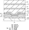
Fig. 1 illustrates the sectional view of the optical semiconductor device that comprises organic EL of this execution mode.As shown in Figure 1, the organic EL of this execution mode has glass substrate 101, on glass substrate 101, is formed with anode electrode 103 and dyke 104 through dielectric film 102.Glass substrate 101 for example comprises quartz, and dielectric film 102 is formed by silicon oxide film.Dyke 104 is the dielectric films that formed by photosensitive polyimide, contacts with the upper surface of dielectric film 102.Anode electrode 103 for example is by aluminium and indium tin oxide (ITO:Indium-Tin-Oxide) being stacked gradually the range upon range of film formed conductive layer that forms, contacting with the upper surface of dielectric film 120.Dyke 104 has the peristome that is cone angle, and the upper surface of anode electrode 103 exposes in the bottom of above-mentioned peristome.But the side of anode electrode 103 is covered by dyke 104.In addition, for example be quartz at these parts that glass substrate 101 has been described, but glass substrate 101 also can be a resin substrate.
Forming organic EL layer 105 on the anode electrode 103 and on the dyke 104.Organic EL layer 105 contacts with the upper surface of anode electrode 103 in the bottom of above-mentioned peristome, form the anode electrode 103 that covering exposes from above-mentioned peristome upper surface, have the part of upper surface of inwall and dyke 104 of the cone angle of above-mentioned peristome.Organic EL layer 105 is the luminescent layers that constitute from the stacked film of anode electrode 103 sides range upon range of hole injection layer, hole transporting layer, luminescent layer, electron supplying layer and electron injecting layer by comprising, at this above-mentioned stacked film is concentrated to describe as organic EL layer 105.
On the organic EL layer 105 and on the dyke 104, cathode electrode 106 and VUV light absorbing zone 107 have been formed successively to cover organic EL layer 105 from glass substrate 101 sides.Cathode electrode 106 is the conductive layers that formed by the Ag-Mg alloy with 20nm left and right sides thickness.VUV light absorbing zone 107 forms covered cathode electrode 106, in addition, form overlook observe with organic EL layer 105 overlapping.That is, VUV light absorbing zone 107 be formed at organic EL layer 105 directly over.In addition, VUV light absorbing zone 107 is formed by silicon oxynitride film, has the thickness about 150nm.
On VUV light absorbing zone 107, buffer film 108, barrier film 109, buffer film 110, barrier film 111 and buffer film 112 have been stacked gradually from glass substrate 101 sides.Buffer film 108,110,112 and barrier film 109,111 constitute diaphragm seal, and barrier film mainly is the barrier film to moisture.As shown in Figure 1, on organic EL layer 105, multilayer buffer film and barrier film arranged from glass substrate 101 sides are alternately range upon range of successively.The film density of barrier film 109,111 is greater than buffer film 108,110,112, so water preventing ability is greater than buffer film 108,110,112.At this, buffer film and barrier film unified Definition are diaphragm seal.In addition, the described diaphragm seal of the application is meant and prevents to enter into from the outside moisture of organic EL layer, resin substrate or the film of oxygen.
Buffer film 108,110,112 has a plurality of films upper surface separately and the effect of lower surface planarization that constitutes diaphragm seal that make.This be because, it is mobile that buffer film 108,110,112 represent in manufacturing process, the substrate of buffer film 108 forms concavo-convexly owing to the peristome of dyke 104, the upper surface of buffer film 108 also forms smooth shape.That is to say, though be formed at the bottom surface of the undermost buffer film 108 in the diaphragm seal have concavo-convex, its upper surface planarization.In addition, Young's modulus is lower than the buffer film the 108,110, the 112nd of barrier film 109,111, makes diaphragm seal integral body become low Young's modulus and has and prevent that diaphragm seal from producing and peel off or the planarization film of the effect that diaphragm seal cracks.
Also not shown in Fig. 1, be formed with the plug and wiring pad that is electrically connected with the outside respectively on the anode electrode 103 and on the cathode electrode 106, formation can apply the structure of voltage respectively independently.In addition, the thickness that barrier film 109,111 all has about 150nm, the thickness that buffer film 108,110,112 all has about 1000nm.
In addition; Buffer film 108,110,112 and the barrier film 109,111 that constitute the organic EL of this execution mode form by silicon oxynitride film; But in order to compare, the organic EL the when buffer film 108,110,112 shown in illustrated later Fig. 1 and barrier film 109,111 are formed by parts such as silicon oxide film and silicon nitride films.
The principal character of the optical semiconductor device of this execution mode is that buffer film 108,110,112 comprises the inorganic nitrogen silicon oxide film through the optical cvd method formation of vacuum-ultraviolet light.Below, the effect of the optical semiconductor device of this execution mode is described.
In the organic EL that sees through as the cathode electrode on the top of the organic EL layer of luminescent layer and the top emission type that diaphragm seal is emitted light, consider that the above-mentioned diaphragm seal that is formed on the organic EL layer has stepped construction.Diaphragm seal need have and prevents that moisture etc. is immersed in the block in the element from the outside, and, constitute interface between each film of stepped construction of diaphragm seal and need have the high flatness that is used for extracting expeditiously the light of emitting from organic EL layer.Possess on top between the anode electrode and diaphragm seal of organic EL layer; Be formed with dyke with peristome that the upper surface that makes organic EL layer exposes; Be formed with concavo-convex greater than above-mentioned peristome at the upper surface of dyke, and, sometimes because etch residues etc. are formed with concavo-convex on dyke.Thereby it is more important that diaphragm seal has following character: guaranteeing water preventing ability and be filled to cover above-mentionedly when concavo-convex, the flatness at the interface between the film of the stepped construction that constitutes diaphragm seal is improved.
Thereby, above-mentioned diaphragm seal consider the silicon nitride film that water preventing ability is good and when forming good fluidity and after formation its upper surface be easy to form the structure that smooth silicon oxide film cascades.But, have like this in the optical semiconductor device of the diaphragm seal that silicon nitride film and silicon oxide film are cascaded, exist because the multipath reflection in the diaphragm seal and the briliancy of organic EL reduces this problem.
For the multipath reflection of the visible light that suppresses to send from organic EL layer, make as far as possible light incident side layer (cathode electrode) material and with diaphragm seal that this material contacts between refringence, emitting side layer (adhesive linkage) material and diminish and get final product with refringence and the refringence between the range upon range of diaphragm seal between the diaphragm seal that this material contacts.In addition, this said light incident side and emitting side be meant from the organic EL layer of the bottom of cathode electrode to above the light of emitting penetrate to adhesive linkage side (emitting side) from cathode electrode side (light incident side) incident.
At this, Figure 12~Figure 14 illustrates the chart as the reflectivity analog result of stepped construction.These charts are the result of calculation of the reflectivity of the stepped construction shown in Fig. 8, the transverse axis of each chart represent the wavelength band of 300nm~900nm, the longitudinal axis represent light in the inside of above-mentioned stepped construction from the reflectivity of lower floor when the upper strata sees through.Fig. 8 is the sectional view as the stepped construction of comparative example; In this stepped construction, on cathode electrode 301, stack gradually silicon oxide film 302a, silicon nitride film 302b, silicon oxide film 303a, silicon nitride film 303b, silicon oxide film 304a, silicon oxide film 304b, silicon oxide film 305a and adhesive linkage 306.The undermost cathode electrode 301 of the stepped construction shown in Fig. 8 and adhesive linkage (resin) 306 refractive index separately of the superiors are 1.7. Silicon nitride film 302b, 303b, 304b are the barrier films that prevents that moisture etc. from immersing, and silicon oxide film 302a, 303a, 304a, 305a have the buffer film (planarization film) that improves the whole flat type of diaphragm seal and reduce the effect of Young's modulus.
Therefore that is, the Young's modulus of buffer film is lower than barrier film, in manufacturing process, has flowability, even the substrate in the zone that forms buffer film forms concavo-convexly, buffer film also forms filling, and this is concavo-convex, and the upper surface of formed buffer film becomes smooth.
Be the analog result that the refractive index with the silicon nitride film 302b shown in Fig. 8,303b, 304b calculates as 1.7 in the chart of Figure 12~Figure 14, transverse axis is represented wavelength, and the longitudinal axis is represented reflectivity.In addition, about the refractive index of silicon oxide film 302a, 303a, 304a, 305a, Figure 12 illustrates the result who calculates as 1.5, and Figure 13 illustrates the result who calculates as 1.55, and Figure 14 illustrates the result who calculates as 1.6.That is, in the chart shown in Figure 12, Figure 13 and Figure 14, can know that the refractive index that makes the silicon oxide film that constitutes diaphragm seal dwindles the variation of the reflectivity of refringence stepped construction successively thus near the refractive index of silicon nitride film, cathode electrode and adhesive linkage.That is to say; Be formed in Figure 12 in the refractive index of silicon oxide film of the stepped construction that calculates compare, the refractive index that is formed in the silicon oxide film of the stepped construction that calculates among Figure 14 become with as 1.7 of the refractive index of above-mentioned silicon nitride film, cathode electrode and adhesive linkage approaching values.In addition, calculate to oversimplify in order making, the refractive index in each wavelength to be made as fixing, calculate as the light absorption that does not have film at this.Chart according to Figure 12~Figure 14 can know that reflectivity diminishes when the refractive index of stacked film diminishes.
In addition, Figure 15 illustrates the relation of maximum reflectivity of refringence and the above-mentioned stacked film of the stacked film that is used in sealing.Figure 15 is the chart of relation of refringence of buffer film and the barrier film of the formation stacked film represented with respect to transverse axis of the maximum reflectivity of the expression longitudinal axis.Can know that according to Figure 14 the maximum reflection rate variance becomes big when refringence becomes big.Numerical value about this reflectivity; With by the light incident side material of light and emit the influence that the change of the refractive index of side material causes and compare; The influence of the multipath reflection that is produced by the difference of the refractive index of stacked film is big especially, can the inhibitory reflex rate through reducing that these refringences come.
For example, be made as the method about 1.7, make silicon oxide film contain nitrogen usually and be made as the method for silicon oxynitride film (SiON film) as the refractive index of the silicon oxide film that will constitute diaphragm seal.But, in the optical cvd method of the organic source that will contain a large amount of carbon, be difficult to obtain the big film of film density, i.e. the block water film (barrier film) big to the block of moisture as unstrpped gas.Thereby, consider according to the aspect of reliability, be desirably in the film that blocks water of range upon range of diaphragm seal and use inoranic membrane.
And; Forming under the situation of silicon oxynitride film through the optical cvd method of using vacuum-ultraviolet light; There is the method that silicone based gas and the gas that becomes oxidation source and nitridation source are reacted; But the delustring area of section of ammonia (NH3) or nitrogen (N2) etc. of unstrpped gas that becomes nitrogen-atoms (N) is little, so the decomposition efficiency of light auxiliary processing is little, thus the silicon oxynitride film of the combination that is difficult to obtain expecting.That is to say, have following problem: forming under the situation of silicon oxynitride film, in formed silicon oxynitride film, can't import the nitrogen of desired amount, be difficult to make refractive index near 1.7 through the optical cvd method of using vacuum-ultraviolet light.Therefore; In this execution mode; Effectively utilize the advantage of the optical cvd film of low stress such as specific heat cvd film or plasma CVD film and low Young's modulus, and obtain good water preventing ability, therefore form silicon oxynitride film (buffer film and barrier film) through the remote plasma auxiliary processing.The plasma auxiliary processing is meant through plasma carries out predecomposition to raw material and under the state of free radical, supplies raw materials and carry out the long-pending film build method of membrane stack thus; In this execution mode, utilize together and used the optical cvd method of unstrpped gas and plasma auxiliary processing to form above-mentioned silicon oxynitride film.In addition, will to utilize free radical and will be processed the situation that surface (substrate) is disposed at from the position that plasma zone (plasma zone) separates and be called remote plasma in order to separate at this.In addition, will carry out predecomposition to raw material through plasma and the situation of supplying raw materials under the state at free radical is called the free radical irradiation at this.
Specifically, in the film forming of buffer film, in the unstrpped gas of optical cvd, use the organosilicon membrane that contains carbon, import nitrogen free radical or nitrogen free radical and the oxygen radical that forms through remote plasma as nitridation source.Thus, can form SiON (silicon oxynitride) film of the advantage of effectively utilizing the optical cvd film.On the other hand; In the forming process of the big SiON film of block; In the unstrpped gas of optical cvd, use the inorganic silicon source that does not comprise carbon such as high-order silane, import nitrogen free radical or nitrogen free radical and the oxygen radical that forms through remote plasma as nitridation source.Thus, can form the big inorganic SiON film of water preventing ability.That is to say that the buffer film the 108,110, the 112nd shown in Fig. 1 comprises the organic nitrogen silicon oxide film of carbon, barrier film the 109, the 111st does not comprise the inorganic nitrogen silicon oxide film of carbon.Use the inorganic nitrogen silicon oxide film that does not comprise carbon to constitute barrier film 109,111, can form the barrier film 109,111 that film density is big, water preventing ability is high thus.
Buffer film 108,110,112 and barrier film 109,111 have used the optical cvd method of vacuum-ultraviolet light and to have used the plasma CVD method of remote plasma and the silicon oxynitride film that forms constitutes by utilizing together.The back specifies the formation method that forms silicon oxynitride film through the optical cvd method of having used the remote plasma auxiliary processing.In addition, the delustring area of section is the degree of absorption difficulty of the light of expression material, and the then easier absorbing light of the material that the delustring area of section is big is more decomposed in the optical cvd method easily.
In the optical semiconductor device of this execution mode; Comprise membrane stress and Young's modulus is little and during the range upon range of diaphragm seal of the big barrier film of buffer film that fillibility is good and water preventing ability in formation; Reduce the refringence of buffer film and barrier film as far as possible, can suppress the multipath reflection in the range upon range of diaphragm seal.In addition, through the refringence between the film that reduces to constitute range upon range of diaphragm seal, can significantly improve the light extraction efficiency of optical semiconductor device.
But; There is following problem: using cathode electrode to form under the situation of diaphragm seal through the optical cvd method on the organic EL layer; The VUV light transmission cathode electrode that shines when forming diaphragm seal arrives organic EL layer, and organic EL layer is impaired and organic EL layer is luminous hardly.The photon energy of the vacuum-ultraviolet light that in the film formation process of optical cvd method, uses is approximately more than the 7eV, also organic EL is brought very macrolesion even see through cathode electrode a little.
(400nm~700nm) requires the transmitance more than 80% for visible light in cathode electrode.In the OLED of top emission type display, consider to use extremely thin alloys such as metallic film, for example Al-Li or Ag-Mg.As the method that suppresses through the vacuum-ultraviolet light of cathode electrode, consider the method for the thickness of increase cathode electrode, but the transmitance of visible light reduces significantly when increasing the thickness of cathode electrode, so the reduction of the briliancy of the organic EL of accomplishing.
Therefore; As shown in Figure 1; In the optical semiconductor device of this execution mode, through VUV light absorbing zone 107 is set on cathode electrode 106, when on cathode electrode 106, forming diaphragm seal through the optical cvd method; Absorb the vacuum-ultraviolet light that the optical cvd methods are used by VUV light absorbing zone 107 in film formation process, thereby prevent that organic EL layer 105 from being sustained damage by vacuum-ultraviolet light.The light deterioration that becomes 10% organic EL layer 105 when above when the transmitance of the vacuum-ultraviolet light that sees through to organic EL layer 105 becomes obvious; Therefore in this execution mode through in the parts of VUV light absorbing zone 107, using silicon oxynitride film, the transmitance inhibition of vacuum-ultraviolet light that will be through organic EL layer 105 is for approximately less than 10%.That is to say that VUV light absorbing zone 107 constitutes by absorbing the dielectric film of vacuum-ultraviolet light more than 90%.Thus, the thickness that does not increase cathode electrode 106 just can prevent the light deterioration of organic EL layer 105.
Like this, in this execution mode, in the film formation process that suppresses the optical cvd film for the light injury of organic EL layer, before carrying out the optical cvd film forming, on organic EL layer, form the absorbed layer of vacuum-ultraviolet light through plasma CVD method.Through forming above-mentioned light absorbing zone, in the time of can significantly suppressing to form range upon range of diaphragm seal by the light injury of vacuum-ultraviolet light for organic EL layer.
Below, use Fig. 1~Fig. 7 to specify this execution mode.At first, as shown in Figure 2, on the glass substrate of being prepared 101, form dielectric film 102.Dielectric film 102 is by with TEOS and O
2(oxygen) forms as the plasma CVD method of unstrpped gas, and for example thickness is made as 200nm.Then, after the stacked film that forms aluminium and indium tin oxide (ITO:Indium-Tin-Oxide), above-mentioned stacked film is processed into predetermined shape, forms anode electrode 103 thus through the dry ecthing method that has used photoetching technique.
Then; As shown in Figure 3; Form on anode electrode 103 and on the dielectric film 102 after the photosensitive polyimide film, process the peristome that the part that forms the upper surface that makes above-mentioned anode electrode 103 is exposed, form thus by the film formed dyke 104 of above-mentioned polyimides through light.Above-mentioned peristome has cone angle, the narrow width of the width ratio open portion topmost of peristome bottom.Like this, form peristome to the mode that the top enlarges with upper surface from the anode electrode 103 that exposed, this be because, in subsequent handling, successfully forming organic EL layer 105 on the anode electrode 103 and on the peristome of dyke 104.That is to say; For example have under the situation of vertical inwall at the interarea of peristome to glass substrate 101; Organic EL layer 105 is along the inwall of peristome and form; And form in the bottom of peristome and top and bend to the right angle, therefore be difficult to form organic EL layer 105 as luminescent layer according to uniform precision.Thereby the peristome of dyke 104 has cone angle, can form organic EL layer 105 with mild angle on the top of peristome.
Afterwards, form the organic EL layer 105 that is electrically connected with anode electrode 103 through the mask evaporation method in the bottom of the above-mentioned peristome of dyke 104.Organic EL layer 105 is made up of the hole injection layer, hole transporting layer, luminescent layer, electron supplying layer and the electron injecting layer that form successively from anode electrode 103 sides, at this these stacked films is concentrated to describe as organic EL layer 105.In this execution mode, in organic EL layer 105, use the low molecular material of fluorescence radiation, but the present invention is not the invention relevant with organic EL layer, therefore, omits the detailed description relevant with the material of organic EL layer 105 at this.
Then; As shown in Figure 4; Form by after the film formed cathode electrode 106 of the Ag-Mg alloy of thickness 20nm through the mask evaporation method on dyke 104 and on the organic EL layer 105, on anode electrode 106, form by the film formed VUV light absorbing zone 107 of silicon oxynitride through plasma CVD method.In this execution mode; In the forming process of VUV light absorbing zone 107, used silane (SiH4), nitrogen, oxygen as the ICP-CVD of the inductance coupling high type of unstrpped gas (Inductively Coupled Plasma-CVD: the method for inductively coupled plasma-CVD); If but organic EL layer 105 is not brought fire damage (about below 100 ℃) or plasma damage etc., then also can pass through CCP-CVD (Capacitively Coupled Plasma-CVD) method or the formation such as sputtering method or vapour deposition method of other method, for example capacitive coupling type.In this execution mode, become VUV light absorbing zone 107 silicon oxynitride film, wavelength is made as 1.7 for the refractive index of the light of 632.8nm, and its thickness is made as 150nm.In addition, the visible light that produces of the gas laser apparatus that only uses He-Ne of wavelength 632.8nm.
Then, use the film formation device shown in Fig. 5 on VUV light absorbing zone 107, to form diaphragm seal, form the structure shown in Fig. 7 thus with stepped construction.At this, on organic EL layer 105 through cathode electrode 106 and VUV light absorbing zone 107 from alternately range upon range of successively multilayer buffer film of organic EL layer 105 sides and barrier film.That is to say; As shown in Figure 7; On VUV light absorbing zone 107, form the buffer film 108 of thickness 1000nm, the barrier film 109 of thickness 150nm, the buffer film 110 of thickness 1000nm, the barrier film 111 of thickness 150nm and the buffer film 112 of thickness 1000nm successively, form the above-mentioned diaphragm seal that forms by these buffer films 108,110,112 and barrier film 109,111 thus.
Substrate forming buffer film 108 is formed with VUV light absorbing zone 107, but the surface of above-mentioned substrate is owing to the peristome that is had by dyke 104 has concaveconvex shape.Above-mentioned diaphragm seal becomes the path of the light that sends of organic EL, therefore needs to suppress the diffusion and the reflection of the light in the above-mentioned diaphragm seal, and expectation has with respect to the main surface parallel of glass substrate 101 and smooth upper surface.At this; When film forming, form the mobile buffer film 108 of expression; Thus when filling the concaveconvex shape of above-mentioned substrate; The upper surface of buffer film 108 can form smooth shape, therefore can formed thereon the buffer film and the upper surface and the bottom surface of barrier film be made as and the main surface parallel of glass substrate 101 and smooth shape.
In addition; Except the concaveconvex shape that produces by above-mentioned peristome; Before the formation of buffer film 108, being formed at foreign matters such as etch residue or dust on the glass substrate 101 also is cushioned film 108 and fills; Therefore the concavo-convex of substrate that is formed at buffer film 108 distorted the interface between the film that constitutes diaphragm seal, can prevent that thus the briliancy of organic EL from reducing.
In addition, directly forming in the substrate that has this foreign matter under the situation of barrier film that fillibility is lower than buffer film, considering that the generations such as side of substrate surface and above-mentioned foreign matter under above-mentioned foreign matter do not form the gap of barrier film.Barrier film is the film that blocks water that is used to prevent the immersion of moisture, is therefore producing under the local situation that does not produce the such gap of barrier film, and organic EL is for the tolerance deterioration of moisture and the reliability of optical semiconductor device reduces.For this; As stated; Before forming barrier film 109, form and have mobile buffer film 108; Make and surround above-mentioned foreign matter even under substrate surface forms the situation of foreign matter, also can form buffer film 108 thus, therefore can prevent to be formed at the barrier film 109 generation gaps on the buffer film 108 and the water preventing ability of organic EL reduces.
At this, Fig. 5 illustrates the sketch map of the film formation device in the formation of the above-mentioned diaphragm seal that is used in this execution mode.Film formation device shown in Fig. 5 is made up of the reative cell 501 with vacuum exhaust mechanism 508 and pressure control mechanism, synthetic quartz window 503, VUV light modulation unit 504, remote plasma introducing port 505a, 505b, gas introduction port 506a, 506b and band temperature control pedestal 507.Import at outside various free radicals, the for example nitrogen free radical (N that produces of device from remote plasma introducing port 505a, 505b
*), oxygen radical (O
*), argon free radical (Ar
*) etc.In this execution mode, in VUV light modulation unit 504, use Xe
2(wavelength=172nm) carries out film forming to Excimer lamp.In addition, as shown in Figure 5, in film formation process, be configured in the top that the band temperature is controlled pedestal 507 as the substrate (glass substrate) 502 that carries out the object of film forming.In addition, each structure of the film formation device shown in Fig. 5 is controlled by controller 509.That is, controller 509 is devices of the effect that has flow (influx) to above-mentioned various free radicals, control to the voltage application of VUV light modulation unit 504 and the temperature of band temperature control pedestal 507 etc.
In addition, Fig. 6 illustrates the table of the membrane structure of the diaphragm seal of studying in this execution mode of explanation.The unstrpped gas that is used in film forming is shown in the bracket in the drawings.At this, as organosilicon source illustration OMCTS (Octo methyl cyclotetrasiloxane: octamethylcy-clotetrasiloxane) and BTBAS (Bis (tertiary butyl amino) silane: two (cyclopropylamino) silane), as inorganic silicon source illustration Si
2H
6(disilane), these are in the preference, the unstrpped gas that is used in the film forming of diaphragm seal is not limited to these unstrpped gas.As the gas that obtains with the OMCTS same effect; Tetraethyl silica alkane), HMDSO (Hexa methyl disiloxane: HMDO) etc. for example there is TEOS (Tetra ethoxy silane:; HMDS), TMCTS (Tetra methyl cyclotetrasiloxane: tetramethyl-ring tetrasiloxane) etc. as the gas that obtains with the BTBAS same effect, can also use HMDS (Hexa methyl disilazane:.
At this, as the combination of the membrane structure of buffer film that constitutes diaphragm seal and barrier film, the membrane structure A~D combination separately that goes out the table of Fig. 6 as an illustration.
Membrane structure A shown in Fig. 6 be to use silicon oxide film in the buffer film, to using the structure of silicon nitride film in the barrier film, the situation that forms identical membrane structure is also on the books in patent documentation 1.The silicon oxide film that in membrane structure A, constitutes buffer film forms through the optical cvd method of having used OMCTS, and the silicon nitride film that constitutes barrier film forms through the optical cvd method of having used BTBAS.
In addition, the membrane structure B shown in Fig. 6 be to use silicon oxide film in the buffer film, to using the structure of silicon oxynitride film in the barrier film.The silicon oxide film that in membrane structure B, constitutes buffer film forms through the optical cvd method of having used OMCTS, and the silicon oxynitride film that constitutes barrier film is through having used Si
2H
6, O
*And N
*The auxiliary optical cvd method of plasma form.In addition, the O of front
*And N
*Represent oxygen radical and nitrogen free radical respectively.
In addition, membrane structure C shown in Fig. 6 and membrane structure D are all to using silicon oxynitride film in buffer film and the barrier film.Membrane structure C or membrane structure D are all through having used Si
2H
6, O
*And N
*The auxiliary optical cvd method of plasma to form this point identical with barrier film, but the formation gas of buffer film is different with barrier film.In membrane structure C, use OMCTS and N
*Form silicon oxynitride film, in membrane structure D, use BTBAS and O
*Form silicon oxynitride film.OMCTS and BTBAS as the raw material in the formation that is used in buffer film in membrane structure C and membrane structure D have methyl and ethyl respectively, are the organic material that comprises carbon, and be relative therewith, as the Si of the raw material in the formation that is used in barrier film
2H
6(high-order silane) gas is the inorganic material that does not comprise carbon (C).
Below; Explanation is applied to the buffer film of Fig. 1 and the manufacturing approach under the situation in the barrier film with four groups the membrane structure of the A~D shown in Fig. 6, and the reflectivity and the light extraction efficiency (briliancy) that illustrate the diaphragm seal that forms through each membrane structure compare the result who obtains.
As shown in Figure 5, each style (substrate 502) that forms VUV light absorbing zone 107 through the operation of using Fig. 4 explanation is transported on the band temperature control pedestal 507 in the reative cell 501 of keeping vacuum, carries out film forming according to predetermined order.At this moment, substrate 502 is controlled to be desired temperatures by band temperature control pedestal 507.Organic EL layer have can't be luminous because of about 100 ℃ heat deterioration character, so substrate 502 is remained 50 by band temperature control pedestals 507.About C.In film formation process, do not use under the situation of plasma auxiliary processing of remote plasma; Carry out after the pressure adjustment 504 irradiation vacuum-ultraviolet lights from VUV light modulation unit and begin film forming unstrpped gas being imported to reative cell 501 from gas introduction port 506a, 506b.On the other hand; In the method for using the plasma auxiliary processing; Carry out unstrpped gas being imported to reative cell 501 after the pressure adjustment from gas introduction port 506a, 506b; Carry out the plasma auxiliary processing when 504 pairs of substrates 502 shine vacuum-ultraviolet lights from VUV light modulation unit, begin film forming thus.That is to say, in the irradiation process of vacuum-ultraviolet light, used the plasma irradiating of remote plasma.
In membrane structure A, import OMCTS from gas introduction port 506a, 504 irradiation Xe from VUV light modulation unit
2Lamp and on substrate 502, forming by the film formed buffer film 108 of silica.Then, import BTBAS, 504 irradiation Xe from VUV light modulation unit from gas introduction port 506b
2Lamp and on substrate 502, forming by the film formed barrier film 109 of silicon nitride.Through identical method, on substrate 502, form buffer film (silicon oxide film) 110, barrier film (silicon nitride film) 111 and buffer film (silicon oxide film) 112 successively.
In membrane structure B, import OMCTS from gas introduction port 506a, 504 irradiation Xe from VUV light modulation unit
2Lamp and on substrate 502, forming by the film formed buffer film 108 of silica.Then, import Si from gas introduction port 506b
2H
6, import N from remote plasma introducing port 505a
*, import O from remote plasma introducing port 505b
*, 504 irradiation Xe from VUV light modulation unit
2Lamp and on substrate 502, forming by the film formed barrier film 109 of silicon oxynitride.Through identical method, on substrate 502, form buffer film (silicon oxide film) 110, barrier film (silicon oxynitride film) 111 and buffer film (silicon oxide film) 112 successively.
In membrane structure C, import OMCTS from gas introduction port 506a, import N from remote plasma introducing port 505a
*, 504 irradiation Xe from VUV light modulation unit
2Lamp and on substrate 502, forming by the film formed buffer film 108 of silicon oxynitride.Then, import Si from gas introduction port 506b
2H
6, import N from remote plasma introducing port 505a
*, import O from remote plasma introducing port 505b
*, 504 irradiation Xe from VUV light modulation unit
2Lamp and on substrate 502, forming by the film formed barrier film 109 of silicon oxynitride.Through identical method, on substrate 502, form buffer film (silicon oxynitride film) 110, barrier film (silicon oxynitride film) 111 and buffer film (silicon oxynitride film) 112 successively.In addition, also can import N at 108,110,112 o'clock at the formation buffer film from remote plasma introducing port 505a
*, and from remote plasma introducing port 505b importing O
*
In membrane structure D, import BABAS from gas introduction port 506b, import O from remote plasma introducing port 505b
*, 504 irradiation Xe from VUV light modulation unit
2Lamp and on substrate 502, forming by the film formed buffer film 108 of silicon oxynitride.Then, import Si from gas introduction port 506b
2H
6, import N from remote plasma introducing port 505a
*, import O from remote plasma introducing port 505b
*, 504 irradiation Xe from VUV light modulation unit
2Lamp and on substrate 502, forming by the film formed barrier film 109 of silicon oxynitride.Through identical method, on substrate 502, form buffer film (silicon oxynitride film) 110, barrier film (silicon oxynitride film) 111 and buffer film (silicon oxynitride film) 112 successively.In addition, also can import N at 108,110,112 o'clock at the formation buffer film from remote plasma introducing port 505a
*, and from remote plasma introducing port 505b importing O
*
Each layer that forms through said method, be following refractive index for the refractive index of the light of wavelength 632.8nm.The refractive index of the buffer film of membrane structure A, B (silicon oxide film) is 1.44, and the refractive index of the buffer film of membrane structure A (silicon nitride film) is 1.92.On the other hand, the refractive index of the buffer film of membrane structure C, D (silicon oxynitride film) is 1.65, and the refractive index of the buffer film of membrane structure B, C (silicon oxynitride film) is 1.7.
According to The above results, in the optical semiconductor device of above-mentioned execution mode, in the structure of buffer film shown in Fig. 1 and barrier film, adopt the structure of membrane structure C or D and be not to adopt membrane structure A, the B shown in Fig. 6.That is to say that membrane structure C shown in Fig. 6 and D are to use the membrane structure in this execution mode, membrane structure A and B are the membrane structures of comparative example.Thereby in the organic EL of this execution mode, buffer film 108,110,112 shown in Fig. 1 and barrier film 109,111 form by the silicon oxynitride film that forms through the optical cvd method of having used the plasma auxiliary processing.
The combination of the silicon oxynitride film in this execution mode and refractive index (absorption coefficient) can be passed through silicon class unstrpped gas and oxygen radical (O
*) and nitrogen free radical (N
*) flow recently adjust.In addition, the example of oxygen radical as oxidation source is being provided shown in this execution mode, but the decomposition efficiency of oxygen against vacuum ultraviolet light high (the delustring area of section is big) therefore is not oxygen radical is provided and provides oxygen and can form silicon oxynitride film yet.That is, through above-mentioned each gas flow ratio being adjusted, can be formed silicon oxynitride film with expectation combination, refractive index (absorption coefficient).In the time of for example can and forming the buffer film of membrane structure D when forming the buffer film of the membrane structure C of Fig. 6, D, using is not to use oxygen radical and the method for using oxygen like this.
Afterwards,, form the wiring (not shown) that the anode electrode shown in Fig. 7 103 is connected with cathode electrode 106 respectively, accomplish the major part of the organic EL of this execution mode thus through technique known.
According to the method for above explanation, below the result that the briliancy under the situation of electronics compares is injected in explanation in will four kinds of organic ELs to buffer film with the membrane structure A shown in Fig. 6~D structure separately and barrier film under the same conditions.At first, as shown in Figure 1, under situation about comparing with the style structure that forms VUV light absorbing zone 107, the expression style of high briliancy is the style of membrane structure C and membrane structure D, all representes roughly the same briliancy.Relative therewith, only obtain 20%~30% the briliancy of membrane structure C as the membrane structure B of comparative example, only obtain 8%~15% the briliancy of membrane structure C as the membrane structure A of comparative example.
And, above-mentioned style at relative humidity 90%, 80 ℃ environment held certain hour, will be compared for the briliancy variation of initial luminance.Its result, the briliancy of membrane structure C, D almost do not change, and relative therewith, membrane structure B is reduced to 90%~95% briliancy, and membrane structure A is reduced to 70%~80% briliancy.As stated, the optical semiconductor device according to this execution mode of the diaphragm seal with membrane structure C or D can improve the light extraction efficiency (briliancy) of organic EL, and can improve the reliability to moisture.
In this execution mode; An example that forms the film (barrier film) that blocks water through the optical cvd method of having used the remote plasma auxiliary processing is shown; But according to the viewpoint of light extraction efficiency (refractive index control) or water preventing ability (film density), even use other film build method to obtain identical effect.For example, if make substrate, be the upper surface planarization of buffer film 108 through forming the mobile big buffer film 108 shown in Fig. 1, then also can be through the plasma CVD method use barrier film 109,111 of step lining property not as the optical cvd method.But, as shown in this execution mode, if in same device continuously film forming constitute the buffer film and the barrier film of diaphragm seal, then can significantly boost productivity.
In addition, in this execution mode, the refractive index of the buffer film 108,110,112 that will form through the optical cvd method of using the remote plasma auxiliary processing is made as 1.65, but the setting of film combination of considering other characteristic is indispensable.Specifically, in the film forming of carrying out through the optical cvd method of having used the organosilicon source, refractive index increases when the nitrogen content in the increase film, but the mobile deterioration of film shows the trend that membrane stress and Young's modulus increase.That is, in buffer film, require good flatness, be used to prevent to crack this opposite character of inhibition that also requires the multipath reflection in the range upon range of diaphragm seal in the low stress peeled off with film, the Young's modulus.Present inventor people considers to study on the above-mentioned project foundation; Confirmed following situation: if the refringence between barrier film and the buffer film with respect to the light of wavelength 632.8nm in the scope below 0.25, then obtain good light extraction efficiency (briliancy) and can not produce the crackle of film or peel off.
Then, the style of the formation VUV light absorbing zone 107 shown in Fig. 1 and the style that does not form the VUV light absorbing zone shown in Figure 16 are compared.Figure 16 is the sectional view as the optical semiconductor device shown in the comparative example; Both all have the structure of the membrane structure A of the identical Fig. 6 of the membrane structure of diaphragm seal, but it is different with the organic El device of this execution mode in the organic EL of the comparative example shown in Figure 16, not form UV Absorption layer this point on the top of cathode electrode 206.That is to say that except not forming UV Absorption layer this point, the organic EL shown in Figure 16 has the structure identical with the organic EL shown in Fig. 1.
The diaphragm seal of the style of the formation VUV light absorbing zone 107 shown in Fig. 1 is the membrane structure shown in Fig. 6; Therefore but to compare briliancy little luminous with membrane structure C, D; Relative therewith, it is luminous hardly not form the style shown in Figure 16 of VUV light absorbing zone 107.This be because, in the forming process of the buffer film 208 of the initial process that forms operation as diaphragm seal, the vacuum-ultraviolet light that in the optical cvd method, uses brings light injury through 206 pairs of organic EL layers 205 of cathode electrode.Relative therewith, in this execution mode, that kind as shown in Figure 1 is provided with VUV light absorbing zone 107 directly over organic EL layer 105, can form diaphragm seal and organic EL layer not brought light injury through the optical cvd method thus.
In the example of in the parts of VUV light absorbing zone 107, using silicon oxynitride film shown in this execution mode, but the parts of VUV light absorbing zone 107 differ and are decided to be silicon oxynitride film, also can be made up of other parts.According to present inventor people's research, if the transmitance of the vacuum-ultraviolet light through organic EL layer 105 then almost can't see the light deterioration of organic EL layer approximately less than 10%.In addition, strictly speaking, cathode electrode on the organic EL layer absorbs 5% of vacuum-ultraviolet light, and therefore when 5% when above of the vacuum-ultraviolet light through organic EL layer of becoming, organic EL layer receives light injury, thus generation light deterioration.
Thereby, if absorb vacuum-ultraviolet light 90% or more and organic EL layer 105 is not brought the dielectric film of light injury, then can also use silicon oxynitride film film kind in addition.For example, for example use aluminium oxide, aluminium nitride or silicon oxynitride aluminium etc. also can access same effect.But, consider the employed film kind absorption coefficient of light separately, need to set required thickness.
In addition, in this execution mode, in other plasma CVD equipment, formed the film forming of VUV light absorbing zone 107, but can also in the device shown in Fig. 5, form.For example, be following method: import Si from gas introduction port 506a
2H
6Gas, import N from remote plasma introducing port 505a
*, import O from remote plasma introducing port 505b
*, do not carry out light irradiation and form silicon oxynitride film through vacuum-ultraviolet light lamp unit 504.Do not carry out rayed so film forming speed and descend, but Si
2H
6Gas reacts with the free radical that imports from remote plasma, therefore can recently form silicon oxynitride film through the adjustment gas flow.In this case, can concentrate formation, therefore have effects such as whole productivity ratio raising of technology and the reduction of plant investment cost through the device identical with diaphragm seal.
As stated; In the organic EL of this execution mode; Structure through membrane structure C shown in Fig. 6 or D forms buffer film 108,110,112 shown in Fig. 1 and barrier film 109,111; Through reducing buffer film and barrier film, buffer film and cathode electrode and buffer film and adhesive linkage refringence separately, can suppress the multipath reflection of the light in the diaphragm seal thus, improve the light extraction efficiency (briliancy) of organic EL.
As stated, buffer film and barrier film can be made up of the silicon oxynitride film that forms through the optical cvd method of having used the remote plasma auxiliary processing, can reduce the refringence of buffer film and barrier film thus.In not using the common optical cvd method of remote plasma auxiliary processing; The such little unstrpped gas of delustring area of section of ammonia or nitrogen is decomposed and extracted nitrogen; With this nitrogen import to want film forming film the difficulty; But through using the film formation device shown in Fig. 5, use the remote plasma auxiliary processing that nitrogen free radical etc. is provided, can form the silicon oxynitride film of expectation thus.
More than, according to the specifically clear invention of being undertaken by the inventor of execution mode, but the present invention is not limited to above-mentioned execution mode, obviously in the scope that does not break away from its aim, can carry out various changes.
For example, use the optical cvd method to form diaphragm seal in the above-described embodiment, therefore need prevent organic EL layer to be brought damage by the vacuum-ultraviolet light that is used in the optical cvd method.In the above-described embodiment, such VUV light absorbing zone 107 that forms as shown in Figure 1 can prevent owing to form vacuum-ultraviolet light and organic EL layer 105 deteriorations of buffer film 108,110,112 and barrier film irradiation in 109,111 o'clock not luminous thus.
In addition, in the above-described embodiment, gone out to form the optical semiconductor device of organic EL and diaphragm seal thereof, still, can also above-mentioned diaphragm seal has been applied to possess in the OLED display of thin-film transistor certainly as an illustration.For example, the switch element that is made up of thin-film transistor is set between glass substrate shown in Fig. 1 101 and dielectric film 102, above-mentioned switch element is connected with organic EL, can form organic EL thus.
In addition; The surface and the back side through at resin molding, resin substrate form diaphragm seal of the present invention; Come to suppress the dimensional variations that the moisture absorption by resin molding or resin substrate etc. causes; In addition, can also be to the formation of foregoing invention above-mentioned resin molding or the resin substrate etc. of diaphragm seal make up with OLED display and form flexible OLED display.In this case, after forming the structure shown in Fig. 1, remove glass substrate 101, then carried out bonding by having with the resin substrate of the diaphragm seal covering of the buffer film shown in Fig. 1 and barrier film same structure and the bottom of anode electrode 102 surface.In addition, likewise, can also the diaphragm seal of above-mentioned execution mode be applied to organic EL illumination certainly.Particularly, as this execution mode, visible light through the device structure of diaphragm seal in effect become obvious.
In addition, at the top of organic EL layer configuration cathode electrode, disposed anode electrode in the above-described embodiment in the bottom of organic EL layer, still, on the contrary, also can be at the top of organic EL layer configuration anode electrode and at the bottom of organic EL layer configuration cathode electrode.
Utilizability on the industry
The manufacturing approach of optical semiconductor device of the present invention extensively is used in the optical semiconductor device that has through the diaphragm seal of visible light.
Claims (16)
1. optical semiconductor device; Have on substrate first electrode, organic luminous layer, second electrode that form successively from the interarea side of aforesaid substrate; And be arranged on the aforesaid substrate to cover the diaphragm seal of above-mentioned luminescent layer, this optical semiconductor device is characterised in that
Above-mentioned diaphragm seal comprises the stacked film that alternately range upon range of planarization film and barrier film form,
Above-mentioned planarization film and above-mentioned barrier film comprise silicon oxynitride film.
2. optical semiconductor device according to claim 1 is characterized in that,
The upper surface of above-mentioned first electrode exposes from the peristome that is formed at first dielectric film between above-mentioned planarization film and the aforesaid substrate; The bottom surface that is formed at the undermost above-mentioned planarization film on the above-mentioned peristome has concavo-convex, and the upper surface of undermost above-mentioned planarization film is smooth.
3. optical semiconductor device according to claim 1 is characterized in that,
Above-mentioned planarization film comprises the silicon oxynitride film that contains carbon,
Above-mentioned barrier film comprises the inorganic nitrogen silicon oxide film.
4. optical semiconductor device according to claim 1 is characterized in that,
Above-mentioned planarization film utilizes vacuum ultraviolet optical cvd method and utilizes the plasma CVD method of remote plasma to form through also using.
5. optical semiconductor device according to claim 1 is characterized in that,
Above-mentioned barrier film utilizes vacuum ultraviolet optical cvd method and utilizes the plasma CVD method of remote plasma to form through also using.
6. optical semiconductor device according to claim 1 is characterized in that,
Specific Young's modulus is low mutually with above-mentioned barrier film for above-mentioned planarization film, and above-mentioned barrier film is compared film density with above-mentioned planarization film big and water preventing ability is high.
7. optical semiconductor device according to claim 1 is characterized in that,
Between above-mentioned organic luminous layer and above-mentioned diaphragm seal, be formed with second dielectric film that absorbs vacuum-ultraviolet light.
8. optical semiconductor device according to claim 7 is characterized in that,
Above-mentioned second dielectric film is to absorb the dielectric film of vacuum ultraviolet more than 90%.
9. the manufacturing approach of an optical semiconductor device is characterized in that, has following operation:
(a) on substrate, form first electrode;
(b) on above-mentioned first electrode, form the organic luminous layer that is connected with above-mentioned first electrode electricity;
(c) on above-mentioned organic luminous layer, form second electrode that is electrically connected with above-mentioned organic luminous layer; And
(d) on above-mentioned organic luminous layer, form silicon oxynitride film through the optical cvd method of utilizing vacuum-ultraviolet light,
Wherein, in above-mentioned (d) operation, in the irradiation process of above-mentioned vacuum-ultraviolet light, utilize remote plasma to carry out the free radical irradiation.
10. the manufacturing approach of optical semiconductor device according to claim 9 is characterized in that,
In above-mentioned (d) operation; The above-mentioned silicon oxynitride film of range upon range of multilayer, on above-mentioned organic luminous layer from the alternately laminated successively barrier film that comprises the planarization film of one of a plurality of above-mentioned silicon oxynitride films and comprise one of a plurality of above-mentioned silicon oxynitride films of above-mentioned organic luminous layer side.
11. the manufacturing approach of optical semiconductor device according to claim 10 is characterized in that,
In above-mentioned (d) operation, the organic substance that will have carbon forms above-mentioned planarization film as raw material, only inorganic matter is formed above-mentioned barrier film as raw material.
12. the manufacturing approach of optical semiconductor device according to claim 10 is characterized in that,
Above-mentioned planarization film is in forming process, to show mobile film, and above-mentioned barrier film is to compare the film that film density is big and water preventing ability is high with above-mentioned planarization film.
13. the manufacturing approach of optical semiconductor device according to claim 9 is characterized in that,
After above-mentioned (a) operation, before above-mentioned (b) operation, also has following operation: on aforesaid substrate, form after first dielectric film, the upper surface of above-mentioned first electrode is exposed the above-mentioned first dielectric film opening.
14. the manufacturing approach of optical semiconductor device according to claim 9 is characterized in that,
In above-mentioned (d) operation, at least one in use nitrogen free radical and the oxygen radical and organosilicon gas are as the unstrpped gas that forms above-mentioned silicon oxynitride film.
15. the manufacturing approach of optical semiconductor device according to claim 9 is characterized in that,
In above-mentioned (d) operation, use some, high-order silane gas and nitrogen free radical in oxygen radical or the oxygen, as the unstrpped gas that forms above-mentioned silicon oxynitride film.
16. the manufacturing approach of optical semiconductor device according to claim 9 is characterized in that,
Before above-mentioned (d) operation, also has following operation: on above-mentioned organic luminous layer, form second dielectric film of absorption vacuum ultraviolet more than 90%.
Applications Claiming Priority (2)
| Application Number | Priority Date | Filing Date | Title |
|---|---|---|---|
| JP2011-081553 | 2011-04-01 | ||
| JP2011081553A JP2012216452A (en) | 2011-04-01 | 2011-04-01 | Optical semiconductor device and method of manufacturing the same |
Publications (1)
| Publication Number | Publication Date |
|---|---|
| CN102738408A true CN102738408A (en) | 2012-10-17 |
Family
ID=46926025
Family Applications (1)
| Application Number | Title | Priority Date | Filing Date |
|---|---|---|---|
| CN2012100974368A Pending CN102738408A (en) | 2011-04-01 | 2012-03-30 | Optical semiconductor device and manufacturing method thereof |
Country Status (5)
| Country | Link |
|---|---|
| US (1) | US20120248422A1 (en) |
| JP (1) | JP2012216452A (en) |
| KR (1) | KR101366449B1 (en) |
| CN (1) | CN102738408A (en) |
| TW (1) | TW201301606A (en) |
Cited By (7)
| Publication number | Priority date | Publication date | Assignee | Title |
|---|---|---|---|---|
| CN103811525A (en) * | 2012-11-14 | 2014-05-21 | 乐金显示有限公司 | Organic light emitting display device and method of manufacturing the same |
| CN104659054A (en) * | 2013-11-15 | 2015-05-27 | 三星显示有限公司 | Flexible display apparatus and manufacture method thereof |
| CN104752441A (en) * | 2015-03-20 | 2015-07-01 | 京东方科技集团股份有限公司 | Array substrate, manufacturing method thereof, display panel and display device |
| CN105679787A (en) * | 2014-11-18 | 2016-06-15 | 群创光电股份有限公司 | Organic light-emitting diode display device and manufacturing method thereof |
| CN106575664A (en) * | 2014-08-09 | 2017-04-19 | 乐金显示有限公司 | Rollable organic light emitting diode display device |
| CN109326738A (en) * | 2018-09-30 | 2019-02-12 | 云谷(固安)科技有限公司 | The manufacturing method of display panel, display device and display panel |
| CN110783495A (en) * | 2018-07-24 | 2020-02-11 | 三星显示有限公司 | Display device manufacturing method and display device manufacturing system |
Families Citing this family (24)
| Publication number | Priority date | Publication date | Assignee | Title |
|---|---|---|---|---|
| KR101502206B1 (en) | 2012-11-20 | 2015-03-12 | 삼성디스플레이 주식회사 | Organic light emitting display device having improved light emitting efficiency |
| US9692010B2 (en) | 2012-11-20 | 2017-06-27 | Samsung Display Co., Ltd. | Organic light emitting display device |
| KR101410102B1 (en) | 2012-11-20 | 2014-06-27 | 삼성디스플레이 주식회사 | Organic light emitting display device |
| US9349988B2 (en) | 2012-11-20 | 2016-05-24 | Samsung Display Co., Ltd. | Organic light emitting display device |
| KR102092557B1 (en) * | 2012-12-12 | 2020-03-24 | 엘지디스플레이 주식회사 | Organic light emitting device and method for manufacturing the same |
| JP6054763B2 (en) | 2013-02-12 | 2016-12-27 | 株式会社ジャパンディスプレイ | Organic EL display device |
| TWI578592B (en) * | 2013-03-12 | 2017-04-11 | 應用材料股份有限公司 | Organic light-emitting diode device and method of deposition an encapsulation structure having the same |
| JP2016523442A (en) * | 2013-06-29 | 2016-08-08 | アイクストロン、エスイー | High performance coating deposition method and encapsulated electronic device |
| US20150014663A1 (en) * | 2013-07-11 | 2015-01-15 | Korea Institute Of Science And Technology | Organic light emitting display apparatus and the method for manufacturing the same |
| KR101588298B1 (en) * | 2013-07-11 | 2016-02-12 | 한국과학기술연구원 | Organic light emitting display apparatus and the method for manufacturing the same |
| DE102014102565B4 (en) * | 2014-02-27 | 2019-10-24 | Osram Oled Gmbh | Optoelectronic component and method for producing an optoelectronic component |
| KR102203910B1 (en) * | 2014-10-22 | 2021-01-14 | 엘지디스플레이 주식회사 | Rollable organic light emitting diode disaplay device |
| KR20160036722A (en) | 2014-09-25 | 2016-04-05 | 삼성디스플레이 주식회사 | organic light emitting diode display and manufacturing method thereof |
| TWI595692B (en) * | 2014-11-18 | 2017-08-11 | 群創光電股份有限公司 | Organic light emitting diode display device and manufacturing method thereof |
| KR102392604B1 (en) * | 2014-12-05 | 2022-04-28 | 엘지디스플레이 주식회사 | Organic light emitting display apparatus and manufacturing the same |
| US9450203B2 (en) | 2014-12-22 | 2016-09-20 | Apple Inc. | Organic light-emitting diode display with glass encapsulation and peripheral welded plastic seal |
| KR102330331B1 (en) * | 2015-07-17 | 2021-11-25 | 삼성디스플레이 주식회사 | Organic luminescence emitting display device and the method of manufacturing the same |
| JP2017105013A (en) * | 2015-12-08 | 2017-06-15 | 株式会社リコー | Gas barrier laminate, semiconductor device, display element, display device and system |
| KR102454027B1 (en) * | 2016-11-06 | 2022-10-14 | 케이엘에이 코포레이션 | Method and apparatus for encapsulation of organic light emitting diodes |
| CN109427992B (en) | 2017-08-28 | 2019-10-18 | 昆山国显光电有限公司 | Thin-film packing structure and display device with it |
| JP6663400B2 (en) * | 2017-09-11 | 2020-03-11 | 株式会社Kokusai Electric | Semiconductor device manufacturing method, substrate processing apparatus, and program |
| US10134709B1 (en) * | 2017-12-21 | 2018-11-20 | Industrial Technology Research Institute | Substrateless light emitting diode (LED) package for size shrinking and increased resolution of display device |
| CN208722925U (en) * | 2018-08-16 | 2019-04-09 | 京东方科技集团股份有限公司 | A kind of encapsulating structure of display device, display device |
| JP2022547125A (en) * | 2019-09-10 | 2022-11-10 | アプライド マテリアルズ インコーポレイテッド | Encapsulation application example of high-density plasma CVD for display |
Citations (2)
| Publication number | Priority date | Publication date | Assignee | Title |
|---|---|---|---|---|
| US20080026198A1 (en) * | 2003-04-17 | 2008-01-31 | Minoru Komada | Barrier film and laminated material, container for wrapping and image display medium using the saw, and manufacturing method for barrier film |
| US20080284331A1 (en) * | 2007-05-17 | 2008-11-20 | Seiko Epson Corporation | Electro-luminescence device and method of manufacturing electro-luminescence device |
Family Cites Families (11)
| Publication number | Priority date | Publication date | Assignee | Title |
|---|---|---|---|---|
| JP4171258B2 (en) * | 2002-07-25 | 2008-10-22 | 三洋電機株式会社 | Organic EL panel |
| JP4138672B2 (en) * | 2003-03-27 | 2008-08-27 | セイコーエプソン株式会社 | Manufacturing method of electro-optical device |
| JP2005267984A (en) * | 2004-03-17 | 2005-09-29 | Sanyo Electric Co Ltd | Organic el display device |
| JP4631683B2 (en) * | 2005-01-17 | 2011-02-16 | セイコーエプソン株式会社 | Light emitting device and electronic device |
| JP4763400B2 (en) * | 2005-09-22 | 2011-08-31 | 株式会社巴川製紙所 | Clay thin film substrate, clay thin film substrate with electrode, and display element using them |
| JP4600254B2 (en) * | 2005-11-22 | 2010-12-15 | セイコーエプソン株式会社 | LIGHT EMITTING DEVICE AND ELECTRONIC DEVICE |
| CA2657232A1 (en) * | 2006-07-07 | 2008-01-10 | University Of Miami | Enhanced oxygen cell culture platforms |
| JP2008153004A (en) * | 2006-12-15 | 2008-07-03 | Konica Minolta Holdings Inc | Organic electroluminescent element |
| CN101697343B (en) * | 2009-10-27 | 2011-06-15 | 苏州纳科显示技术有限公司 | Film encapsulation method |
| US20110244128A1 (en) * | 2010-03-31 | 2011-10-06 | Tokyo Electron Limited | Flow plate utilization in filament assisted chemical vapor deposition |
| US9299956B2 (en) * | 2012-06-13 | 2016-03-29 | Aixtron, Inc. | Method for deposition of high-performance coatings and encapsulated electronic devices |
-
2011
- 2011-04-01 JP JP2011081553A patent/JP2012216452A/en active Pending
-
2012
- 2012-03-20 TW TW101109488A patent/TW201301606A/en unknown
- 2012-03-22 KR KR1020120029220A patent/KR101366449B1/en active IP Right Grant
- 2012-03-28 US US13/432,678 patent/US20120248422A1/en not_active Abandoned
- 2012-03-30 CN CN2012100974368A patent/CN102738408A/en active Pending
Patent Citations (2)
| Publication number | Priority date | Publication date | Assignee | Title |
|---|---|---|---|---|
| US20080026198A1 (en) * | 2003-04-17 | 2008-01-31 | Minoru Komada | Barrier film and laminated material, container for wrapping and image display medium using the saw, and manufacturing method for barrier film |
| US20080284331A1 (en) * | 2007-05-17 | 2008-11-20 | Seiko Epson Corporation | Electro-luminescence device and method of manufacturing electro-luminescence device |
Cited By (15)
| Publication number | Priority date | Publication date | Assignee | Title |
|---|---|---|---|---|
| CN103811525B (en) * | 2012-11-14 | 2016-12-28 | 乐金显示有限公司 | Oganic light-emitting display device and the method manufacturing this oganic light-emitting display device |
| CN103811525A (en) * | 2012-11-14 | 2014-05-21 | 乐金显示有限公司 | Organic light emitting display device and method of manufacturing the same |
| US9570517B2 (en) | 2012-11-14 | 2017-02-14 | Lg Display Co., Ltd. | Organic light emitting display device and method of manufacturing the same |
| CN104659054A (en) * | 2013-11-15 | 2015-05-27 | 三星显示有限公司 | Flexible display apparatus and manufacture method thereof |
| US10186681B2 (en) | 2014-08-09 | 2019-01-22 | Lg Display Co., Ltd. | Rollable organic light emitting diode display device |
| CN106575664A (en) * | 2014-08-09 | 2017-04-19 | 乐金显示有限公司 | Rollable organic light emitting diode display device |
| CN106575664B (en) * | 2014-08-09 | 2019-09-10 | 乐金显示有限公司 | Rollable organic LED display device |
| CN105679787A (en) * | 2014-11-18 | 2016-06-15 | 群创光电股份有限公司 | Organic light-emitting diode display device and manufacturing method thereof |
| CN105679787B (en) * | 2014-11-18 | 2018-09-25 | 群创光电股份有限公司 | Organic LED display device and its manufacturing method |
| CN104752441B (en) * | 2015-03-20 | 2018-03-16 | 京东方科技集团股份有限公司 | A kind of array base palte and preparation method thereof, display panel and display device |
| CN104752441A (en) * | 2015-03-20 | 2015-07-01 | 京东方科技集团股份有限公司 | Array substrate, manufacturing method thereof, display panel and display device |
| CN110783495A (en) * | 2018-07-24 | 2020-02-11 | 三星显示有限公司 | Display device manufacturing method and display device manufacturing system |
| CN109326738A (en) * | 2018-09-30 | 2019-02-12 | 云谷(固安)科技有限公司 | The manufacturing method of display panel, display device and display panel |
| CN109326738B (en) * | 2018-09-30 | 2020-02-11 | 云谷(固安)科技有限公司 | Display panel, display device and manufacturing method of display panel |
| US11469398B2 (en) | 2018-09-30 | 2022-10-11 | Yungu (Gu'an) Technology Co., Ltd. | Display panel, display device and method of manufacturing display panel |
Also Published As
| Publication number | Publication date |
|---|---|
| KR101366449B1 (en) | 2014-02-25 |
| US20120248422A1 (en) | 2012-10-04 |
| TW201301606A (en) | 2013-01-01 |
| JP2012216452A (en) | 2012-11-08 |
| KR20120112056A (en) | 2012-10-11 |
Similar Documents
| Publication | Publication Date | Title |
|---|---|---|
| CN102738408A (en) | Optical semiconductor device and manufacturing method thereof | |
| US11871607B2 (en) | Electronic device with reduced non-device edge area | |
| JP6370816B2 (en) | High performance coating deposition equipment | |
| US7518142B2 (en) | Encapsulation for organic device | |
| KR101526083B1 (en) | Gas-barrier film, method for producing gas-barrier film, and electronic device | |
| CN104798220B (en) | For manufacturing the method for layer in the surface region of electronic device | |
| US20190221771A1 (en) | Buffer layer for organic light emitting devices and method of making the same | |
| CN111769206A (en) | Thin film permeation barrier system for substrates and devices and method of making the same | |
| TW201705492A (en) | Thin film transistor | |
| Park et al. | High-performance thin H: SiON OLED encapsulation layer deposited by PECVD at low temperature | |
| US10005263B2 (en) | Display device and method of manufacturing a display device | |
| KR102108560B1 (en) | Method for preparing a barrier film | |
| CN105190932A (en) | Improvement of barrier film performance with n2o dilution process for thin film encapsulation | |
| KR102139077B1 (en) | Gas barrier film and method for manufacturing the same | |
| KR102616238B1 (en) | Nitrogen-rich silicon nitride films for thin-film transistors | |
| TWI634672B (en) | Deposition method of passivation film for light emitting diode | |
| WO2012132585A1 (en) | Gas barrier film, production device therefor, and production program therefor | |
| KR101793897B1 (en) | Deposition method of passivation film for light emitting diode | |
| CN110911586B (en) | OLED panel, preparation method of OLED panel and display device | |
| HO | The Long-term Stability of SiNx Thin Film Encapsulation Layers and Their Effects on the Optical Property of Organic Light Emitting Diode | |
| TW201032337A (en) | Protection of optoelectronic devices and method thereof |
Legal Events
| Date | Code | Title | Description |
|---|---|---|---|
| C06 | Publication | ||
| PB01 | Publication | ||
| C10 | Entry into substantive examination | ||
| SE01 | Entry into force of request for substantive examination | ||
| C02 | Deemed withdrawal of patent application after publication (patent law 2001) | ||
| WD01 | Invention patent application deemed withdrawn after publication |
Application publication date: 20121017 |