JP2016523442A - High performance coating deposition method and encapsulated electronic device - Google Patents
High performance coating deposition method and encapsulated electronic device Download PDFInfo
- Publication number
- JP2016523442A JP2016523442A JP2016524299A JP2016524299A JP2016523442A JP 2016523442 A JP2016523442 A JP 2016523442A JP 2016524299 A JP2016524299 A JP 2016524299A JP 2016524299 A JP2016524299 A JP 2016524299A JP 2016523442 A JP2016523442 A JP 2016523442A
- Authority
- JP
- Japan
- Prior art keywords
- layer
- substrate
- given embodiment
- electrodes
- deposition
- Prior art date
- Legal status (The legal status is an assumption and is not a legal conclusion. Google has not performed a legal analysis and makes no representation as to the accuracy of the status listed.)
- Pending
Links
Images


Classifications
-
- H—ELECTRICITY
- H10—SEMICONDUCTOR DEVICES; ELECTRIC SOLID-STATE DEVICES NOT OTHERWISE PROVIDED FOR
- H10K—ORGANIC ELECTRIC SOLID-STATE DEVICES
- H10K50/00—Organic light-emitting devices
- H10K50/80—Constructional details
- H10K50/84—Passivation; Containers; Encapsulations
- H10K50/844—Encapsulations
- H10K50/8445—Encapsulations multilayered coatings having a repetitive structure, e.g. having multiple organic-inorganic bilayers
-
- C—CHEMISTRY; METALLURGY
- C23—COATING METALLIC MATERIAL; COATING MATERIAL WITH METALLIC MATERIAL; CHEMICAL SURFACE TREATMENT; DIFFUSION TREATMENT OF METALLIC MATERIAL; COATING BY VACUUM EVAPORATION, BY SPUTTERING, BY ION IMPLANTATION OR BY CHEMICAL VAPOUR DEPOSITION, IN GENERAL; INHIBITING CORROSION OF METALLIC MATERIAL OR INCRUSTATION IN GENERAL
- C23C—COATING METALLIC MATERIAL; COATING MATERIAL WITH METALLIC MATERIAL; SURFACE TREATMENT OF METALLIC MATERIAL BY DIFFUSION INTO THE SURFACE, BY CHEMICAL CONVERSION OR SUBSTITUTION; COATING BY VACUUM EVAPORATION, BY SPUTTERING, BY ION IMPLANTATION OR BY CHEMICAL VAPOUR DEPOSITION, IN GENERAL
- C23C16/00—Chemical coating by decomposition of gaseous compounds, without leaving reaction products of surface material in the coating, i.e. chemical vapour deposition [CVD] processes
- C23C16/22—Chemical coating by decomposition of gaseous compounds, without leaving reaction products of surface material in the coating, i.e. chemical vapour deposition [CVD] processes characterised by the deposition of inorganic material, other than metallic material
- C23C16/30—Deposition of compounds, mixtures or solid solutions, e.g. borides, carbides, nitrides
- C23C16/308—Oxynitrides
-
- C—CHEMISTRY; METALLURGY
- C23—COATING METALLIC MATERIAL; COATING MATERIAL WITH METALLIC MATERIAL; CHEMICAL SURFACE TREATMENT; DIFFUSION TREATMENT OF METALLIC MATERIAL; COATING BY VACUUM EVAPORATION, BY SPUTTERING, BY ION IMPLANTATION OR BY CHEMICAL VAPOUR DEPOSITION, IN GENERAL; INHIBITING CORROSION OF METALLIC MATERIAL OR INCRUSTATION IN GENERAL
- C23C—COATING METALLIC MATERIAL; COATING MATERIAL WITH METALLIC MATERIAL; SURFACE TREATMENT OF METALLIC MATERIAL BY DIFFUSION INTO THE SURFACE, BY CHEMICAL CONVERSION OR SUBSTITUTION; COATING BY VACUUM EVAPORATION, BY SPUTTERING, BY ION IMPLANTATION OR BY CHEMICAL VAPOUR DEPOSITION, IN GENERAL
- C23C16/00—Chemical coating by decomposition of gaseous compounds, without leaving reaction products of surface material in the coating, i.e. chemical vapour deposition [CVD] processes
- C23C16/22—Chemical coating by decomposition of gaseous compounds, without leaving reaction products of surface material in the coating, i.e. chemical vapour deposition [CVD] processes characterised by the deposition of inorganic material, other than metallic material
- C23C16/30—Deposition of compounds, mixtures or solid solutions, e.g. borides, carbides, nitrides
- C23C16/34—Nitrides
- C23C16/345—Silicon nitride
-
- C—CHEMISTRY; METALLURGY
- C23—COATING METALLIC MATERIAL; COATING MATERIAL WITH METALLIC MATERIAL; CHEMICAL SURFACE TREATMENT; DIFFUSION TREATMENT OF METALLIC MATERIAL; COATING BY VACUUM EVAPORATION, BY SPUTTERING, BY ION IMPLANTATION OR BY CHEMICAL VAPOUR DEPOSITION, IN GENERAL; INHIBITING CORROSION OF METALLIC MATERIAL OR INCRUSTATION IN GENERAL
- C23C—COATING METALLIC MATERIAL; COATING MATERIAL WITH METALLIC MATERIAL; SURFACE TREATMENT OF METALLIC MATERIAL BY DIFFUSION INTO THE SURFACE, BY CHEMICAL CONVERSION OR SUBSTITUTION; COATING BY VACUUM EVAPORATION, BY SPUTTERING, BY ION IMPLANTATION OR BY CHEMICAL VAPOUR DEPOSITION, IN GENERAL
- C23C16/00—Chemical coating by decomposition of gaseous compounds, without leaving reaction products of surface material in the coating, i.e. chemical vapour deposition [CVD] processes
- C23C16/44—Chemical coating by decomposition of gaseous compounds, without leaving reaction products of surface material in the coating, i.e. chemical vapour deposition [CVD] processes characterised by the method of coating
- C23C16/50—Chemical coating by decomposition of gaseous compounds, without leaving reaction products of surface material in the coating, i.e. chemical vapour deposition [CVD] processes characterised by the method of coating using electric discharges
-
- H—ELECTRICITY
- H10—SEMICONDUCTOR DEVICES; ELECTRIC SOLID-STATE DEVICES NOT OTHERWISE PROVIDED FOR
- H10K—ORGANIC ELECTRIC SOLID-STATE DEVICES
- H10K50/00—Organic light-emitting devices
- H10K50/80—Constructional details
- H10K50/84—Passivation; Containers; Encapsulations
- H10K50/842—Containers
- H10K50/8423—Metallic sealing arrangements
-
- H—ELECTRICITY
- H10—SEMICONDUCTOR DEVICES; ELECTRIC SOLID-STATE DEVICES NOT OTHERWISE PROVIDED FOR
- H10K—ORGANIC ELECTRIC SOLID-STATE DEVICES
- H10K71/00—Manufacture or treatment specially adapted for the organic devices covered by this subclass
-
- H—ELECTRICITY
- H10—SEMICONDUCTOR DEVICES; ELECTRIC SOLID-STATE DEVICES NOT OTHERWISE PROVIDED FOR
- H10K—ORGANIC ELECTRIC SOLID-STATE DEVICES
- H10K77/00—Constructional details of devices covered by this subclass and not covered by groups H10K10/80, H10K30/80, H10K50/80 or H10K59/80
- H10K77/10—Substrates, e.g. flexible substrates
- H10K77/111—Flexible substrates
-
- H—ELECTRICITY
- H10—SEMICONDUCTOR DEVICES; ELECTRIC SOLID-STATE DEVICES NOT OTHERWISE PROVIDED FOR
- H10K—ORGANIC ELECTRIC SOLID-STATE DEVICES
- H10K2102/00—Constructional details relating to the organic devices covered by this subclass
-
- H—ELECTRICITY
- H10—SEMICONDUCTOR DEVICES; ELECTRIC SOLID-STATE DEVICES NOT OTHERWISE PROVIDED FOR
- H10K—ORGANIC ELECTRIC SOLID-STATE DEVICES
- H10K2102/00—Constructional details relating to the organic devices covered by this subclass
- H10K2102/301—Details of OLEDs
- H10K2102/311—Flexible OLED
-
- H—ELECTRICITY
- H10—SEMICONDUCTOR DEVICES; ELECTRIC SOLID-STATE DEVICES NOT OTHERWISE PROVIDED FOR
- H10K—ORGANIC ELECTRIC SOLID-STATE DEVICES
- H10K2102/00—Constructional details relating to the organic devices covered by this subclass
- H10K2102/301—Details of OLEDs
- H10K2102/351—Thickness
-
- Y—GENERAL TAGGING OF NEW TECHNOLOGICAL DEVELOPMENTS; GENERAL TAGGING OF CROSS-SECTIONAL TECHNOLOGIES SPANNING OVER SEVERAL SECTIONS OF THE IPC; TECHNICAL SUBJECTS COVERED BY FORMER USPC CROSS-REFERENCE ART COLLECTIONS [XRACs] AND DIGESTS
- Y02—TECHNOLOGIES OR APPLICATIONS FOR MITIGATION OR ADAPTATION AGAINST CLIMATE CHANGE
- Y02E—REDUCTION OF GREENHOUSE GAS [GHG] EMISSIONS, RELATED TO ENERGY GENERATION, TRANSMISSION OR DISTRIBUTION
- Y02E10/00—Energy generation through renewable energy sources
- Y02E10/50—Photovoltaic [PV] energy
- Y02E10/549—Organic PV cells
-
- Y—GENERAL TAGGING OF NEW TECHNOLOGICAL DEVELOPMENTS; GENERAL TAGGING OF CROSS-SECTIONAL TECHNOLOGIES SPANNING OVER SEVERAL SECTIONS OF THE IPC; TECHNICAL SUBJECTS COVERED BY FORMER USPC CROSS-REFERENCE ART COLLECTIONS [XRACs] AND DIGESTS
- Y02—TECHNOLOGIES OR APPLICATIONS FOR MITIGATION OR ADAPTATION AGAINST CLIMATE CHANGE
- Y02P—CLIMATE CHANGE MITIGATION TECHNOLOGIES IN THE PRODUCTION OR PROCESSING OF GOODS
- Y02P70/00—Climate change mitigation technologies in the production process for final industrial or consumer products
- Y02P70/50—Manufacturing or production processes characterised by the final manufactured product
Abstract
ポリマー又は他の材料上に多層構造を形成するための方法が開示され多層構造は光学的機能を付与し又は酸素及び水蒸気への暴露から下層を保護する。新規デバイスも開示され保護多層構造と、AMOLEDディスプレイ、OLED照明又は太陽電池デバイスの双方を含む。保護多層構造自体は基板上に少なくとも3つの極薄層の材料を順次堆積することにより作製でき各極薄層は異なる密度又は組成を具備する。このフィルムの所与の堆積方法では、フィルムの単位厚さ当たりのイオン衝撃のエネルギーを変えることにより多層が堆積される。構造の任意の層が窒化ケイ素、酸化ケイ素、酸窒化ケイ素又は金属窒化物若しくは金属酸化物のうち1又は複数の材料を含むことができる。この利点を享受する特定の商用用途は太陽電池デバイス又は照明及びディスプレイを含む有機発光ダイオード(OLED)の製造を含む。A method for forming a multilayer structure on a polymer or other material is disclosed that provides an optical function or protects the underlying layer from exposure to oxygen and water vapor. New devices are also disclosed and include both protective multilayer structures and AMOLED displays, OLED lighting or solar cell devices. The protective multilayer structure itself can be made by sequentially depositing at least three ultrathin layer materials on a substrate, each ultrathin layer having a different density or composition. In this given film deposition method, multiple layers are deposited by varying the energy of ion bombardment per unit thickness of the film. Any layer of the structure can include one or more materials of silicon nitride, silicon oxide, silicon oxynitride, or metal nitride or metal oxide. Particular commercial applications that enjoy this advantage include the manufacture of organic light emitting diodes (OLEDs) including solar cell devices or lighting and displays.
Description
本願は、2013年6月29日出願の米国仮出願No.61/841,287及び2014年4月7日出願の米国仮出願No.61/976,420の優先権を主張する特許出願であり、ここに参照することによりその内容を包含する。
本発明は、酸素及び水蒸気の透過に対して保護するバリアとして、又は、反射防止性若しくは光フィルタリング性を付与するものとしての高性能コーティングを堆積する方法に関する。
This application is a provisional application filed on June 29, 2013. 61 / 841,287 and US provisional application no. Patent application claiming priority of 61 / 976,420, the contents of which are incorporated herein by reference.
The present invention relates to a method of depositing a high performance coating as a barrier protecting against the transmission of oxygen and water vapor, or as providing antireflection or light filtering properties.
水分、酸素及び他の化学物質に脆弱な対象材料を保護する薄いフィルムが、多くの工業プロセスにおいて普通に使用されている。食料包装材、眼鏡レンズ上のハードコーティング及び窓ガラスから、集積回路、ディスプレイ画面及び太陽電池パネルの保護まで、用途が広がっている。このような薄いフィルムは、緻密で、下層に対する付着性に優れ、かつ、製品寿命の間は亀裂や剥離を生じないことが必要である。所与の事例におけるコーティングは、ハーメチックシール(気密封止構造)であって水蒸気や酸素を浸入させないことが必要であり、この場合、下層である構造やデバイスの微かな領域であってもその機能を損なってしまうような微小ピンホールリークが多すぎてはならない。さらに、バリアが最高の気密性をもつことを要求されるOLEDディスプレイ画面、照明パネル又は有機太陽電池パネル等の最も高価値の用途の多くについては、製造中にその下層が、所与の事例では100℃を僅かに超える温度から、所与のポリマーについては約75℃未満の温度となる場合もある、限界を超える温度に曝されてはならない。フレキシブル回路や画面等の所与の新製品においては、保護を必要とするデバイスがフレキシブル基板材の上に構築されることになるので、保護機能を損なうことなく繰り返し曲げることが可能でなければならない。 Thin films that protect target materials that are vulnerable to moisture, oxygen and other chemicals are commonly used in many industrial processes. Applications range from food packaging materials, hard coatings on eyeglass lenses and glass panes to protection of integrated circuits, display screens and solar panels. Such a thin film needs to be dense, excellent in adhesion to the lower layer, and not to crack or peel during the lifetime of the product. The coating in a given case must be a hermetic seal (hermetic seal structure) and must not allow water vapor or oxygen to enter, in which case its function can be achieved even in subtle structures and devices. There should not be too many pinhole leaks that would damage In addition, for many of the most valuable applications, such as OLED display screens, lighting panels or organic solar panels where the barrier is required to have the highest airtightness, the underlying layer during manufacture is A temperature slightly above 100 ° C. should not be exposed to temperatures beyond the limits, which can be less than about 75 ° C. for a given polymer. For a given new product such as a flexible circuit or screen, the device that needs to be protected will be built on the flexible substrate material, so it must be able to bend repeatedly without compromising the protection function. .
現在、堆積されたコーティングの付着性は、濡れ性の高いポリマー層からなる中間層を最初に設けるか、又は、不活性プラズマに表面を暴露することにより得られる。コストをかなり重視する必要のある用途の場合、このような濡れ性のあるポリマーを使用することは高価すぎるであろうし、多くの安価なプラスチックについては、不活性ガス処理はハードコーティングの適切な付着性の促進に効果が無いことが判明した。従って、コーティングの適切な付着性を確保するためのより効果的かつより安価な方法が必要とされている。 Currently, the adhesion of the deposited coating is obtained by first providing an intermediate layer of a highly wettable polymer layer or by exposing the surface to an inert plasma. For applications where cost is a significant concern, it would be too expensive to use such wettable polymers, and for many inexpensive plastics, inert gas treatment is a good adhesion of the hard coating. It has been found that there is no effect in promoting sex. Therefore, there is a need for a more effective and less expensive method to ensure proper adhesion of the coating.
そのような低温における緻密なハーメチックバリア層の堆積において、基板上へのターゲット材料のスパッタリングは、最も普通に用いられる方法である。この技術は、基板温度が約100度又はそれ未満の基板温度でうまくいくが、この技術は大きな熱を発生するので、生成されるフィルムは、バリアとしてのアモルファス性と効果を備えていないことがしばしばある。プラスチック又はポリマーの基板が厚いために効率的に冷却できない所与の用途では、基板が過熱するのでスパッタリングを行うことはできない。プラズマ増強CVDは、基板の上限温度が約250℃を超える用途では圧倒的に多く使用されてきたが、100℃未満の基板温度で高品質の誘電体の堆積を、商品競争力のある速度で実現することはできていない。 In the deposition of dense hermetic barrier layers at such low temperatures, sputtering of the target material onto the substrate is the most commonly used method. Although this technique works well at substrate temperatures of about 100 degrees or less, this technique generates significant heat so that the resulting film may not have the amorphous nature and effectiveness as a barrier. Often there is. In a given application where the plastic or polymer substrate is thick and cannot be cooled efficiently, sputtering cannot be performed because the substrate overheats. Plasma-enhanced CVD has been overwhelmingly used in applications where the substrate upper temperature exceeds about 250 ° C., but deposits high quality dielectrics at substrate temperatures below 100 ° C. at a competitively competitive rate. It cannot be realized.
ハーメチックカプセル化プロセスについては、幾つかの新規かつ非常に需要のある高価値用途がある。これらの中に、有機及びCIGS太陽電池デバイス(PV)のカプセル化、及び、照明用とディスプレイ(アクティブマトリクスOLED、すなわちAMOLED)用の両方のための有機発光ダイオード(OLED)デバイスのカプセル化がある。これらの用途は全て、可視光に対して高透過性でありかつ水分及び酸素に対して低透過性であることが厳しく要求される。CIGS等の薄膜材料を用いたソーラーパネルや光電変換のための有機ポリマーは、10−4〜10−5gm/m2/日の水蒸気透過率でのカプセル化を要求する。これらの用途においては、最終製品が競争力をもつためにコストが極めて低くなければならない。OLED照明及び有機PVモジュール等の用途では、1m2当たりのコストを約10USドル又はそれ未満とすべきである。なぜなら、このようなパネル又はウェブのトータルコストは、1m2当たり約60USドル未満とし、そして1m2当たり30USドルにまで下げる必要があるからである。CIGSについては、カプセル化コストは1m2当たり15〜20USドルを超えないようにしなければならず、OLEDディスプレイについては、カプセル化コストは1m2当たり100USドル程度でもよい。なぜなら、ディスプレイ画面のトータル製造コストは1m2当たり約1000〜2000USドルの間だからである。 There are several new and very demanding high value applications for the hermetic encapsulation process. Among these are encapsulation of organic and CIGS solar cell devices (PV) and encapsulation of organic light emitting diode (OLED) devices for both lighting and displays (active matrix OLEDs or AMOLEDs) . All these applications are strictly required to be highly permeable to visible light and low permeable to moisture and oxygen. Solar panels using thin film materials such as CIGS and organic polymers for photoelectric conversion require encapsulation at a water vapor transmission rate of 10 −4 to 10 −5 gm / m 2 / day. In these applications, the cost must be very low in order for the final product to be competitive. In applications such as OLED lighting and organic PV modules, it should be about 10US dollars or less the cost per 1 m 2. This is because the total cost of such a panel or web, and less than about 60US dollars per 1 m 2, and it is necessary to reduce to a 30US dollars per 1 m 2. The CIGS, encapsulation costs must not exceed 15~20US dollars per 1 m 2, for OLED displays, encapsulated cost may be two per 100US about $ 1 m. This is because the total production cost of the display screen is because between about 1000~2000US dollars per 1 m 2.
最も需要のある用途は、AMOLEDディスプレイに対するものである。普通に用いられる液晶ディスプレイ(LCD)に比べて、AMOLED技術は多くの利点があり、低消費電力、高コントラスト、広視野角、及び、フレキシブル基板上に作成可能である点が含まれる。しかし、タブレットやラップトップのディスプレイ等に有用な10cm2より大きいAMOLEDディスプレイを高歩留まりで製造可能とする前に解決すべき重要な技術的課題もある。 The most demanding application is for AMOLED displays. Compared to commonly used liquid crystal displays (LCDs), AMOLED technology has many advantages, including low power consumption, high contrast, wide viewing angle, and the ability to create on flexible substrates. However, there is also an important technical problem to be solved before an AMOLED display larger than 10 cm 2 useful for a tablet or laptop display can be manufactured at a high yield.
特に、OLEDの電子放出層に用いられる低仕事関数の金属と、電子輸送層の間の界面は、酸化による損傷に対して極度に脆弱である。従って、大気中において有用な寿命を確保するためには、OLEDディスプレイは、ピンホールが全くなく酸素透過率(OTR)が10−3〜10−5scc(standard cubic centimeter)/m2/日未満でありかつ水蒸気透過率(WVTR)が10−7g/m2/日未満であるようにカプセル化されなければならない。現在、これは、100μm又はそれ以上の厚さのガラス製トップカバーを用いた量産においてのみ可能である。これに対しLCDディスプレイは、水分や酸素に対してそれほど脆弱ではなく、1日当たり0.1scc/m2即ちg/m2オーダーのOTR及びWVTRでカプセル化すればよい。 In particular, the interface between the low work function metal used in the electron emission layer of an OLED and the electron transport layer is extremely vulnerable to oxidative damage. Therefore, to ensure a useful lifetime in the atmosphere, the OLED display has no pinholes and an oxygen transmission rate (OTR) of less than 10 −3 to 10 −5 scc (standard cubic centimeter) / m 2 / day. And must be encapsulated such that the water vapor transmission rate (WVTR) is less than 10 −7 g / m 2 / day. Currently, this is only possible in mass production using a glass top cover with a thickness of 100 μm or more. In contrast, LCD displays are not very vulnerable to moisture and oxygen and may be encapsulated with OTR and WVTR on the order of 0.1 scc / m 2 or g / m 2 per day.
参考として、このようなカプセル化に必要な強度を理解するためのポイントとしては、OLEDディスプレイにおける空気と水分のリーク要求が、10−10scc/秒オーダーのHeリーク率を備えた高真空チャンバのそれに相当するということである。このような高度の真空性能を備えた高真空チャンバは一般的なものではなく、入念な設計を必要とし、金属シールを使用し、かつ、製造コストが高いために、通常は量産されることはない。 As a reference, the point to understand the strength required for such encapsulation is that air and moisture leak requirements in OLED displays are high vacuum chambers with He leak rates on the order of 10 −10 scc / sec. It corresponds to that. High vacuum chambers with such high vacuum performance are not common, require careful design, use metal seals, and are expensive to manufacture, so they are usually not in mass production. Absent.
OLEDディスプレイは、OLED領域に対し周縁シールを具備するトップガラス層を装着することによってガラス基板上に構築されたときは、十分なカプセル化が可能であると言われてきた。この周縁シールは、酸素及び水分の透過やリークをいくらか許容するポリマーをベースとしているので、OLEDを取り囲む部分に酸素及び水分を吸収するための"ゲッタリング"材を必要とする。これは非常に高価な技術(50USドル/m2〜100USドル/m2)であり、スマートフォンやタブレットのような比較的小型で剛体のディスプレイにのみ適用可能である。さらにこのカプセル化技術は、前面と背面が精確に同じ温度に維持されないと、応力に関する不具合も生じる。最後に、ダブルガラスカプセル化法は、ガラスカバーが極めて薄い場合であってもほとんど非フレキシブルである。このことは極めて限定的なことである。なぜなら、最も高価値のOLEDディスプレイは、フレキシブルであって軽量かつ脆弱ではなく、かつ、LCD技術により簡単に作製できない新規かつコンパクトなディスプレイを実現できるものだからである。従って、OLEDにおいてその全ての性能を実現するために、新たなカプセル化方法が求められている。
OLED displays have been said to be capable of sufficient encapsulation when constructed on a glass substrate by mounting a top glass layer with a peripheral seal against the OLED area. Since this peripheral seal is based on a polymer that allows some permeation or leakage of oxygen and moisture, it requires a “gettering” material to absorb oxygen and moisture in the area surrounding the OLED. This is a very expensive technology (50 US dollars /
さらに最近では、プラズマベースのCVD法による他のタイプの"薄いフィルム"のハーメチックコーティングが試みられている。特にそれらは、酸化アルミニウム及び二酸化チタン等の材料のプラズマ増強若しくはプラズマ支援堆積法、又は、原子層堆積(ALD)によりしばしば作製される二酸化ケイ素、窒化ケイ素及び他の材料等の無機誘電体である。これらのフィルムは、堅牢さと耐引っ掻き性に十分な厚さをもつ場合は極めて脆いため、基板の撓みに十分に耐えることができない。さらに、より厚みのある汎用的なPECVD又はPACVD層は、より堅牢ではあるが、表面欠陥のエッジ周りの結合が弱く、基板が撓むときに材料品質が劣るそれらの欠陥の周りに微細クラックを生じる。このような微細クラックは、その後バリア層内に進行して水分のリーク経路となる。 More recently, other types of “thin film” hermetic coatings have been attempted by plasma-based CVD. In particular they are inorganic dielectrics such as silicon dioxide, silicon nitride and other materials often made by plasma enhanced or plasma assisted deposition of materials such as aluminum oxide and titanium dioxide, or atomic layer deposition (ALD). . These films are extremely fragile when they are thick enough for robustness and scratch resistance, and therefore cannot sufficiently withstand the bending of the substrate. In addition, thicker, generic PECVD or PACVD layers are more robust, but have weaker bonds around the edges of surface defects and fine cracks around those defects that have poor material quality when the substrate flexes. Arise. Such fine cracks then proceed into the barrier layer and become a moisture leak path.
コストを低減し、製造歩留まりを向上させ、かつ、照明とディスプレイの両方におけるOLEDの用途を豊富にするために、高真空チャンバと同等の性能を備えた厚さ約30nmと約10μmの間の透明薄膜による大容量製品のカプセル化を可能とする方法及びツールを見出すことが求められている。多くの商用用途に有用と考えられるフレキシブルディスプレイの場合、ハードの無機バリアは、画面が撓むときや前面と背面の温度差が数十℃もあるときのクラックを避けるために、通常、厚さを約100nmよりいくらか薄くする必要がある。大気が最終的に脆弱な材料層に浸入すると、そのデバイスを損傷し、画面や照明パネル上に"ブラックスポット"を形成する。他のバリア材料としては、厚さ10μmまでであるが、可視光に対する高透明度とバリア機能の双方を備えた有機無機混合コーティングもある。 Transparent between about 30 nm and about 10 μm thick with performance comparable to a high vacuum chamber to reduce costs, improve manufacturing yield, and enrich OLED applications in both lighting and display There is a need to find methods and tools that enable the encapsulation of high volume products with thin films. For flexible displays that are considered useful for many commercial applications, hard inorganic barriers are usually thick to avoid cracking when the screen is bent or when the temperature difference between the front and back is tens of degrees Celsius. Needs to be somewhat thinner than about 100 nm. When the atmosphere eventually penetrates into a fragile material layer, it damages the device and creates a “black spot” on the screen or lighting panel. As another barrier material, there is an organic-inorganic mixed coating having a thickness of up to 10 μm but having both high transparency to visible light and a barrier function.
従来技術は、理想的条件下でのOLEDカプセル化の要求を満たす機能を有する薄いバリアフィルムが存在すること示している。無機の窒化物、酸化物、及び酸窒化物を含むフィルムは、それらが透明でもあるので特に適している。特に、酸化アルミニウム、窒化ケイ素及び酸窒化ケイ素が通常用いられる。これらは透明度が高くかつなお実質的に水分を透過させない緻密な誘電体であり、かなりの製造実績のある真空コーティングプロセスにより適用可能である。 The prior art shows that there are thin barrier films that have the function of meeting the requirements of OLED encapsulation under ideal conditions. Films containing inorganic nitrides, oxides, and oxynitrides are particularly suitable because they are also transparent. In particular, aluminum oxide, silicon nitride and silicon oxynitride are usually used. These are dense dielectrics that are highly transparent and yet substantially impermeable to moisture, and can be applied by vacuum coating processes with considerable manufacturing experience.
従来技術の中には、多数のバリア層を用いることによって1つのバリア層内の局所的粒子や他の欠陥の影響を克服するものがある。それはしばしば、無機バリア層の間に平坦化するソフトかつフレキシブルな有機中間層を具備する。有機中間層の事例では、フレキシブルなポリマー中に欠陥を埋没させて、きれいなポリマー面上に新たな各バリア層を堆積させようとする狙いがある。これは、理想的には、連続するバリア層中の欠陥を広く横方向に分離することになるので、酸素及び水の分子の透過における有効行程長が実質的に長くなり、水分がデバイスの全ての層に透過するまでの時間を非常に大きく遅らせることになる。従来技術は、OLEDディスプレイの寿命を(10年まで)延ばすために適切な酸素や水蒸気の透過率(それぞれOTR及びWVTR)を実現するために、中間層とバリアフィルムからなる積層を3〜7回繰り返すことが必要であると示唆している。 Some prior art overcomes the effects of local particles and other defects in one barrier layer by using multiple barrier layers. It often comprises a soft and flexible organic interlayer that planarizes between inorganic barrier layers. In the case of organic interlayers, the aim is to bury defects in a flexible polymer and deposit each new barrier layer on a clean polymer surface. This would ideally result in a wide lateral separation of defects in the continuous barrier layer, so that the effective path length in the permeation of oxygen and water molecules is substantially increased and moisture is present in the entire device. The time until it permeates through the layer is greatly delayed. The prior art has 3 to 7 layers of interlayers and barrier films to achieve appropriate oxygen and water vapor transmission rates (OTR and WVTR, respectively) to extend the lifetime of OLED displays (up to 10 years). It suggests that it is necessary to repeat.
有機PVやCIGSのパネル、モジュール又はシートは、AMOLEDディスプレイ用途よりもさらにコストに影響される。従って、コスト的に有利な薄いフィルムによるカプセル化は、エネルギー変換市場におけるそれらの競争力に重要なコスト低減を可能とするべくより一層重要である。現在、PVパネルの製造コストは、おおよそ1ワット当たり1USドルであるので、パネルコストはおおよそ100〜150USドル/m2である。従って、カプセル化コストは、その約10%〜15%を超えないようにすべきであり、かつ、少なくとも10年そしておそらくは20年以上持続しなければならない。パネルは、太陽光に直接曝されたとき最大に発電するので、これらのパネルのほとんどが、天候や塵そして広い温度範囲(−10℃〜80℃)に対する暴露に耐え得るものでなければならない。さらに、カプセル化は、基板の大きな熱膨張に順応するために伸張可能であることも重要である。二酸化ケイ素及び窒化ケイ素等の非常に薄い(<30nm)無機フィルムは、クラックを生じずにかなり伸張するが、それより厚いフィルムはしばしばクラックを生じる。 Organic PV and CIGS panels, modules or sheets are more cost sensitive than AMOLED display applications. Thus, cost-effective encapsulation with thin films is even more important to enable cost reductions that are critical to their competitiveness in the energy conversion market. Currently, the manufacturing cost of PV panels is approximately 1 US dollar per watt, so the panel cost is approximately 100 to 150 US dollars / m 2 . Therefore, the encapsulation cost should not exceed about 10% to 15% and should last at least 10 years and possibly more than 20 years. Since the panels generate maximum power when exposed directly to sunlight, most of these panels must be able to withstand exposure to weather, dust and a wide temperature range (-10 ° C to 80 ° C). It is also important that the encapsulation is extensible to accommodate the large thermal expansion of the substrate. Very thin (<30 nm) inorganic films such as silicon dioxide and silicon nitride stretch considerably without cracking, whereas thicker films often crack.
このようなパネルの効率は、それらの性能価格比において重要であるので、それらのパネルは、反射光を減らすことでパネルをより効率化できる反射防止コーティングを設けることによって有益性を高められる。さらに、反射防止コーティングが耐引っ掻き性を有するならば、塵の掃除によって光透過性と効率が低下することがないので、有用である。そのような掃除は、効率低下を避けるために年間に何回も行わなければならない。PV機能に有益な上述した様々なコーティングの全てのコストの合計が、おおよそ15〜20USドル/m2でのコスト限度内に収まるべきである。現在のところ、このコスト限度内でコーティングを作製可能な堆積プロセスは知られていない。このようなプロセスが見出されたならば、OPV及びCIGS並びにPV技術に対する大きな推進力を広く与えることとなるであろう。 Since the efficiency of such panels is important in their performance price ratio, they can be enhanced by providing an anti-reflective coating that can make the panels more efficient by reducing reflected light. Furthermore, if the anti-reflective coating is scratch resistant, it is useful because cleaning the dust does not reduce light transmission and efficiency. Such cleaning must be performed many times a year to avoid efficiency loss. The sum of all the costs of the various coatings described above that are beneficial to PV function should fall within the cost limit of approximately 15-20 USD / m 2 . At present, there are no known deposition processes that can produce coatings within this cost limit. If such a process is found, it will provide a great driving force for OPV and CIGS and PV technology.
従って、AMOLEDディスプレイ、OLED照明、及び可能であれば所与のPV技術において、低酸素透過率及び低水分透過率であって適切なバルク特性をもつ薄いバリアフィルムの堆積方法に対する要望がある。さらに、そのような方法が、カプセルの下層への優れた付着性を確保するとともに、開始表面の不完全さによる局所的欠陥の形成を回避できることが必要である。さらに、1m2当たりの欠陥の数が1又はそれ未満のオーダーであり、かつ、コーティングは微細クラックを生じず、バリア機能を損なわずあるいは剥離を生じずに、所与の事例では非常に曲率半径が小さい場合にも撓みに耐え得ることが必要である。 Accordingly, there is a need for a thin barrier film deposition method with low oxygen transmission and low water transmission and suitable bulk properties in AMOLED displays, OLED lighting, and possibly a given PV technology. Furthermore, it is necessary for such a method to ensure excellent adhesion to the lower layer of the capsule and to avoid the formation of local defects due to imperfections in the starting surface. Furthermore, the number of defects per 1 m 2 is 1 or less order, and the coating does not cause fine cracks, without causing impaired without or peeling off the barrier function, very curvature radius in a given case It is necessary to be able to withstand bending even when is small.
本発明は、少なくとも3つの薄層を具備するフレキシブルで透明な付着性のある多層フィルム構造をもった、大型基板、連続的ウェブ又はウェハ用のコーティングであって、以下の経済的に重要な利点のうちの1又は複数を有するものを提供する。
●空気又は水分に脆弱な材料及びデバイスの気密封止性(hermetic:ハーメチック)コーティングであって、実質的にピンホール及びリークがなく、量産におけるコスト競争力が高いものである。このようなコーティングは、クラックを生じることなく撓みに耐え得るものでかつ非常に高温かつ高湿条件に耐え得るならば、より価値がある。
●フレキシブルプラスチックフィルムの光学コーティングであって、剥離、微細クラック又は変色を生じることなく撓み及び/又は大きな温度変化に耐え得るものである。
●水分又は化学物質に脆弱なデバイス上のハード保護コーティングであって、クラック又は剥離を生じることなく屋外又は大きな温度変化の条件に耐え得るものである。
The present invention is a coating for large substrates, continuous webs or wafers with a flexible, transparent, adherent multilayer film structure comprising at least three thin layers, with the following economically important advantages: One or more of the above are provided.
A hermetic coating of materials and devices that are fragile to air or moisture, with virtually no pinholes and leaks and high cost competitiveness in mass production. Such a coating is more valuable if it can withstand bending without cracking and can withstand very high temperature and humidity conditions.
An optical coating of a flexible plastic film that can withstand bending and / or large temperature changes without delamination, microcracks or discoloration.
A hard protective coating on devices that are vulnerable to moisture or chemicals that can withstand conditions of outdoor or large temperature changes without cracking or peeling.
上記の品質のうち1又は複数を備えたコーティングプロセスは、急速に成長するコストに敏感な市場における、以下を含む特定の適用範囲に使用可能である。しかしながら、これらに限定するものではない。
1.剛体基板又はフレキシブル基板のいずれかの上におけるOLEDディスプレイデバイスのカプセル化。
2.OLED照明デバイスのカプセル化。
3.屋外エネルギー獲得のための薄膜太陽電池(PV)デバイスのカプセル化及び/又は反射防止コーティング及び/又はハードコーティング。それらの中で最も有用なものは、有機PV膜又は銅インジウムガリウムジセレン(CIGS)PVを有するモジュール又は連続ウェブ基板である。
4.窓又は他の屋外使用のためのプラスチック(アクリル及びPET等の最も安価なプラスチックを含む)のハードコーティング又は保護コーティング。クラックや剥離を生じることなく広い温度範囲と湿度範囲に耐える性能が要求される。
Coating processes with one or more of the above qualities can be used for specific applications in the rapidly growing cost sensitive market including: However, it is not limited to these.
1. Encapsulation of an OLED display device on either a rigid substrate or a flexible substrate.
2. Encapsulation of OLED lighting devices.
3. Encapsulation and / or antireflection coating and / or hard coating of thin film solar cell (PV) devices for outdoor energy capture. Among them, the most useful are modules or continuous web substrates with organic PV films or copper indium gallium diselen (CIGS) PV.
4). Hard coating or protective coating of plastic for windows or other outdoor use (including the least expensive plastics such as acrylic and PET). The ability to withstand a wide temperature range and humidity range without causing cracks or peeling is required.
本発明は、以下の図面を参照してさらに説明されるが、それらの図面は本発明の所定の態様を示すことを意図したものであり、本発明の実施形態を限定するものとみなすべきではない。 The present invention will be further described with reference to the following drawings, which are intended to illustrate certain aspects of the invention and should not be considered as limiting embodiments of the invention. Absent.
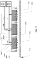
本発明は、大型基板、連続ウェブ、又はウェハのコーティングであって、少なくとも3つの薄層を具備するフレキシブルで透明かつ付着性をもつ多層フィルム構造を有するコーティングを提供する。それらの薄層は、次の経済的に重要な利点を有するものである。
●空気又は水分に脆弱な材料及びデバイスのハーメチック(気密封止性)コーティングであって、実質的にピンホール及びリークがなく、量産におけるコスト競争力が高いものである。このようなコーティングは、クラックを生じることなく撓みに耐え得るものでかつ非常に高温かつ高湿条件に耐え得るならば、より価値がある。
●フレキシブルプラスチックフィルムの光学コーティングであって、剥離、微細クラック又は変色を生じることなく撓み及び/又は大きな温度変化に耐え得るものである。
●水分又は化学物質に脆弱なデバイス上のハード保護コーティングであって、クラック又は剥離を生じることなく屋外又は大きな温度変化の条件に耐え得るものである。
The present invention provides a coating on a large substrate, continuous web, or wafer having a flexible, transparent and adherent multilayer film structure comprising at least three thin layers. These thin layers have the following economically important advantages.
● Hermetic (hermetic sealing) coating of materials and devices that are fragile to air or moisture, substantially free of pinholes and leaks, and highly cost competitive in mass production. Such a coating is more valuable if it can withstand bending without cracking and can withstand very high temperature and humidity conditions.
An optical coating of a flexible plastic film that can withstand bending and / or large temperature changes without delamination, microcracks or discoloration.
A hard protective coating on devices that are vulnerable to moisture or chemicals that can withstand conditions of outdoor or large temperature changes without cracking or peeling.
本方法による利点を享受できる適用例は、有機発光ダイオード(OLED)ディスプレイ及び照明における超低透過性カプセル化に対するニーズである。別の例としては、水分から保護しかつ入射光に対する反射防止機能を付与することによりモジュールの出力が向上する、CIGS太陽電池パネルにおけるコーティングがある。 An application that can benefit from the method is the need for ultra-low-transmission encapsulation in organic light emitting diode (OLED) displays and lighting. Another example is a coating on a CIGS solar panel that protects against moisture and improves the output of the module by providing an antireflection function for incident light.
1又は複数の上記特性を備えたコーティングプロセスは、急成長するコストに敏感な市場における以下の特定の適用範囲に使用可能であるが、これらに限定するものではない。
●剛体基板又はフレキシブル基板のいずれかの上におけるOLEDディスプレイデバイスのカプセル化。
●OLED照明デバイスのカプセル化。
●屋外エネルギー獲得のための薄膜太陽電池(PV)デバイスのカプセル化及び/又は反射防止コーティング及び/又はハードコーティング。それらの中で最も有用なものは、有機PV膜又は銅インジウムガリウムジセレン(CIGS)PVを有するモジュール又は連続ウェブ基板である。
●窓又は他の屋外使用のためのプラスチック(アクリル及びPET等の最も安価なプラスチックを含む)のハードコーティング又は保護コーティング。クラックや剥離を生じることなく広い温度範囲と湿度範囲に耐える性能が要求される。
A coating process with one or more of the above properties can be used for the following specific applications in a rapidly growing cost sensitive market, but is not limited to these.
Encapsulation of OLED display devices on either rigid or flexible substrates.
● Encapsulation of OLED lighting devices.
Encapsulation and / or anti-reflection coating and / or hard coating of thin film solar cell (PV) devices for outdoor energy capture. Among them, the most useful are modules or continuous web substrates with organic PV films or copper indium gallium diselen (CIGS) PV.
Hard coating or protective coating of plastic for windows or other outdoor use (including the least expensive plastics such as acrylic and PET). The ability to withstand a wide temperature range and humidity range without causing cracks or peeling is required.
数値の範囲が示される場合、当該範囲は、当該範囲の端点のみを包含するのではなく、当該範囲に明示的に含まれかつ当該範囲の最後の有効数字により変化する、当該範囲の中間値も包含することを意図している。例えば、1から4の範囲というときは、1〜2、1〜3、2〜4、3〜4及び1〜4を含むことを意図している。 Where a range of numerical values is indicated, the range does not include only the end points of the range, but also includes intermediate values of the range that are explicitly included in the range and vary with the last significant digit of the range. It is intended to be included. For example, a range from 1 to 4 is intended to include 1-2, 1-3, 2-4, 3-4 and 1-4.
本明細書で"約"という用語を用いる場合は、当該単位における当該数値の±15%の範囲内で変更する値も含むことを意図している。 When the term “about” is used herein, it is intended to include values that vary within ± 15% of the value in the unit.
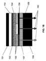
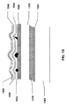
本発明の実施形態は、ポリマー又は他の材料上に、光学的機能を付与するとともに酸素及び水蒸気への暴露から下層を保護する多層構造を形成する方法を開示する。新規デバイスも開示され、それらには、多層保護構造、AMOLEDディスプレイ、OLED照明、又は、太陽電池デバイスが含まれる。開示された保護構造の重要な利点は、基板が繰り返し撓んでも、屋外環境へ曝されてもクラックや剥離を生じないことである。開示された方法及び新規デバイスは、保護構造の堆積ステップに先立ってクリーニングステップ及び表面修飾ステップを含むことができ、また、保護構造の堆積ステップに先立って、保護構造を後で堆積するためにより滑らかな表面とする1又は複数の堆積ステップを含むことができる。多層保護構造自体は、基板上に少なくとも3つの異なる密度又は組成をもつ材料の極薄層を順次堆積することにより形成することができる。多層保護構造の実施形態では、ハード層とソフト層を交互に堆積することにより、又は、フィルム中に含有される窒素又は酸素の濃度が高いものと低いものを交互に堆積することにより形成できる。このようなフィルムを堆積するための開示された方法の所与の実施形態においては、このようなフィルムの単位厚さ当たりのイオン衝撃エネルギーを変化させることにより多層が堆積される。保護構造のいずれの層も、1又は複数の材料を含むことができ、それらの材料は窒化ケイ素、酸化ケイ素、酸窒化ケイ素、又は、金属窒化物若しくは金属酸化物である。 Embodiments of the present invention disclose a method of forming a multilayer structure on a polymer or other material that provides optical functionality and protects the underlying layer from exposure to oxygen and water vapor. Novel devices are also disclosed, including multi-layer protective structures, AMOLED displays, OLED lighting, or solar cell devices. An important advantage of the disclosed protective structure is that it will not crack or peel when the substrate is repeatedly bent or exposed to the outdoor environment. The disclosed method and novel device may include a cleaning step and a surface modification step prior to the protective structure deposition step, and may be smoother to later deposit the protective structure prior to the protective structure deposition step. One or more deposition steps can be included to provide a smooth surface. The multilayer protective structure itself can be formed by sequentially depositing ultrathin layers of materials having at least three different densities or compositions on the substrate. In embodiments of the multilayer protective structure, it can be formed by alternately depositing hard and soft layers, or by alternately depositing high and low concentrations of nitrogen or oxygen contained in the film. In a given embodiment of the disclosed method for depositing such films, multiple layers are deposited by varying the ion bombardment energy per unit thickness of such films. Any layer of the protective structure can include one or more materials, which are silicon nitride, silicon oxide, silicon oxynitride, or metal nitride or metal oxide.
OLEDデバイス等や他の水分に弱いデバイス等の、欠陥に影響されやすいカプセル化用途における所与の実施形態においては、開示された新規の方法が、真空蒸着された多層フィルムであって優れた耐透過性(10−3g/m2/日より良好)をもちながら、汎用的な無機フィルムよりも良好なフレキシビリティを有する実質的に無機のコーティング構造を作製する。開示された方法は、コーティング内のピンホールリークを大きく低減しかつ基板が撓んだ際のコーティングの微細クラックを回避することにより、このことを実現する。開示された堆積プロセス及び方法は、この驚くべきかつ重要なフレキシビリティを無機フィルムであっても実現しており、厚さ100nm〜1000nmの比較的厚いバリアフィルムにおいてフレキシビリティが良好である点で注目すべきである。さらにこのことは、現在又は従来の技術より遙かに低い製造コストで、開示された方法により非常に低い基板温度で非常に低透過率のフィルムに対して行われることによって、多くの重要な量産製品が、より高い競争力で生産される。所与の実施形態では、コーティングのフレキシビリティは、1又は複数の層の堆積中における1又は複数の層への少量の炭素ドーピング(CHx)の含有によりさらに向上させられる。その堆積方法は、純粋な無機の層であれ、炭素を少量ドープされた層であれ、カプセル化プロセスでフィルム中に取り込まれた粒子の近傍に生じるピンホールリーク欠陥を、何千回の撓みの後でさえ大きく低減する。このような粒子は、コーティングシステム内に由来するか又は前回の処理に起因するもので、コーティングシステムに入り込むと基板表面上に存在する。 In a given embodiment in an encapsulation application that is susceptible to defects, such as OLED devices and other moisture-sensitive devices, the disclosed novel method is a vacuum deposited multilayer film that has excellent resistance. A substantially inorganic coating structure is produced that has permeability (better than 10 −3 g / m 2 / day) while having better flexibility than a general purpose inorganic film. The disclosed method accomplishes this by greatly reducing pinhole leakage in the coating and avoiding microcracking of the coating when the substrate is deflected. The disclosed deposition process and method achieves this surprising and important flexibility even for inorganic films, noting that it has good flexibility in relatively thick barrier films with a thickness of 100 nm to 1000 nm. Should. In addition, this can be done for many important mass productions by performing the disclosed method on very low transmission films at very low substrate temperatures with much lower manufacturing costs than current or prior art. Products are produced with higher competitiveness. In a given embodiment, the flexibility of the coating is further improved by the inclusion of a small amount of carbon doping (CH x ) in the one or more layers during the deposition of the one or more layers. Its deposition method, whether it is a pure inorganic layer or a lightly doped layer of carbon, eliminates pinhole leak defects that occur in the vicinity of particles encapsulated in the film during the encapsulation process, with thousands of deflections. Even after it is greatly reduced. Such particles originate from the coating system or are due to previous processing and are present on the substrate surface upon entering the coating system.
本発明の所与の実施形態においては、コーティング構造が実質的に多層ケイ素ベースの誘電体材料であり、その場合、多層の化学組成は層から層へと僅かしか変化しない一方、他のフィルム特性は層から層へと組成に比べてより大きく変化するようにできる。所与の実施形態においては、個々の層のいずれも厚さを約5nmと200nmの間とすることができる。所与の実施形態においては、層から層への組成の変化よりも大きく変化する他の材料特性として、材料密度、主成分の化学量論的組成、微細構造、及びフィルム内在応力がある。所与の実施形態においては、非透過性に優れより大きい圧縮内在応力を有するより高密度材料の薄層と、より透過性でより小さい圧縮内在応力又は引張内在応力を有するより低密度材料の薄層とを交互にすることができる。所与の実施形態においては、層から層への化学量論的組成をフィルム中で変化させることができ、その場合、主成分の相対的濃度のみを変化させる。そのような実施形態の一例として窒化ケイ素フィルムがあり、その場合、ケイ素対窒素の比率が、幾つかの層における約0.65から、他の隣接する1又は複数の層における約0.85まで変化する。同様に、層から層への他の材料特性における変化としては、幾つかの層における、炭素、酸素、窒素、フッ素である1又は複数の元素の少量の混合や濃度変化があり、それらはフィルムの主成分ではない。実質的に酸窒化ケイ素又は窒化ケイ素の多層コーティングである所与の実施形態においては、より多くの酸素(<窒素濃度の20%)を混合した層が、若干少ない酸素(<窒素濃度の5%)を有する層と交互になっている。所与の実施形態においては、より透過性のある多層は、同等の厚さのプラスチックよりは実質的に透過率を小さくすることができ、かつ汎用プラズマ堆積による二酸化ケイ素に対しては透過率において同等か又は大きくすることができる。所与の実施形態においては、その構造の幾つかの層はさらに、ホウ素、ヒ素、リン、イオウ、並びに、アルミニウム、亜鉛、スズ、インジウム、銅、ベリリウム等の金属ドーパントである少量のドーパントを含むことができる。本発明の所与の実施形態では、多層の主成分の組成を、1つの層から次の層へと20%未満で変化させることができる。所与の実施形態では、多層は、層から層へと、屈折率又は光吸収率を10%未満の差で僅かだけ変化させることができ、それにより可視光が、大きな内部界面反射を生じることなく多層の積層を通過することができる。 In a given embodiment of the present invention, the coating structure is substantially a multilayer silicon-based dielectric material, in which case the multilayer chemical composition varies slightly from layer to layer, while other film properties. Can be changed more greatly from layer to layer compared to the composition. In a given embodiment, any of the individual layers can be between about 5 nm and 200 nm thick. In a given embodiment, other material properties that change more than layer-to-layer composition change are material density, principal component stoichiometry, microstructure, and film intrinsic stress. In a given embodiment, a thin layer of a higher density material that is highly impermeable and has a higher compressive intrinsic stress, and a thinner layer of a lower density material that is more permeable and has a lower compressive or tensile intrinsic stress. Layers can be alternated. In a given embodiment, the stoichiometric composition from layer to layer can be varied in the film, in which case only the relative concentrations of the main components are varied. An example of such an embodiment is a silicon nitride film, in which the silicon to nitrogen ratio is from about 0.65 in some layers to about 0.85 in other adjacent layers. Change. Similarly, changes in other material properties from layer to layer include minor mixing or concentration changes of one or more elements that are carbon, oxygen, nitrogen, fluorine in some layers, such as film Is not the main component. In a given embodiment that is substantially a multi-layer coating of silicon oxynitride or silicon nitride, a layer mixed with more oxygen (<20% of the nitrogen concentration) has a slightly lower oxygen (<5% of the nitrogen concentration). ) With alternating layers. In a given embodiment, a more permeable multilayer can be substantially less transmissive than comparable thickness plastic, and in transmission for general purpose plasma deposited silicon dioxide. Can be equivalent or larger. In a given embodiment, some layers of the structure further include boron, arsenic, phosphorus, sulfur, and small amounts of dopants that are metallic dopants such as aluminum, zinc, tin, indium, copper, beryllium. be able to. In a given embodiment of the present invention, the composition of the major components of the multilayer can be changed from one layer to the next by less than 20%. In a given embodiment, the multilayer can change the index of refraction or light absorption slightly from layer to layer with a difference of less than 10%, so that visible light causes large internal interface reflections. And can pass through multiple layers.
所与の実施形態では、このようなコーティング構造を、幾つかの層がその堆積中に表面上でのフィルム成長速度に対して比較的大きい量のイオン衝撃に曝され、かつ、他の幾つかの層の材料が表面上での材料成長速度に対して同程度の量のイオン衝撃に曝されないようなプロセスにより形成することができる。所与の実施形態では、このような多層が、実質的に同じガス混合物を有する複数の所定タイプのプラズマソースから移動基板上に堆積されてもよいが、その場合、堆積速度とイオン衝撃パワーが、基板の移動方向に沿って空間的に変化する。所与の実施形態においては、このような多層構造がプラズマソースにより静止基板上に堆積してもよく、その場合、プラズマソースパワー若しくはガス混合物又はそれらの両方のいずれかが時間的にほぼ段階的方式で変化することにより、堆積速度若しくはイオン衝撃又はそれらの両方のいずれかが層から層へと変化することができる。このような材料は、イオン衝撃パワー密度若しくは堆積速度又はそれらの両方のいずれかにおける層間での急激な変化を伴って、又は、層間での有限の遷移時間により生じる層特性変化のいくらかの長さ範囲を伴って、交互に堆積することができる。 In a given embodiment, such a coating structure is exposed to a relatively large amount of ion bombardment with respect to the film growth rate on the surface during deposition of some layers, and several others. Can be formed by a process that does not expose the material to the same amount of ion bombardment as the material growth rate on the surface. In a given embodiment, such multilayers may be deposited on a moving substrate from multiple predetermined types of plasma sources having substantially the same gas mixture, in which case the deposition rate and ion bombardment power are And spatially change along the moving direction of the substrate. In a given embodiment, such a multilayer structure may be deposited on a stationary substrate by a plasma source, in which case either the plasma source power or the gas mixture or both are approximately stepped in time. By changing in a manner, either the deposition rate or ion bombardment or both can be changed from layer to layer. Such materials have some length of change in layer properties, either with abrupt changes between layers, either in ion bombardment power density or deposition rate, or both, or due to finite transition times between layers. It can be deposited alternately with a range.
イオン衝撃パワー密度対フィルム成長速度の比率が、プラズマ堆積フィルムの密度、微細構造及び応力を決定するファクタであって、そのフィルムの組成は重要度が低いことは周知である。従って、フィルム堆積中にイオン衝撃パワー密度対フィルム成長速度の比率を変えることによって、透過率及び機械的特性において幾つかの層と他の層の間に差異が生じる。基板位置又は基板上でのイオン衝撃と成長速度が一定であるか又はゆっくりと変化し、堆積速度又はイオン衝撃の時間的に急激な変化により分離されるような所与の実施形態では、堆積されるフィルムは、フィルム特性が一定である厚いバンドと、それらの間にあってフィルム特性が遷移する非常に薄いバンドとをもった多層構造を示す。 It is well known that the ratio of ion bombardment power density to film growth rate is a factor that determines the density, microstructure and stress of a plasma deposited film, and that the composition of the film is less important. Thus, changing the ratio of ion bombardment power density to film growth rate during film deposition creates differences between some layers and others in transmission and mechanical properties. In a given embodiment where the ion bombardment and growth rate on the substrate or on the substrate is constant or changes slowly and is separated by a rapid change in deposition rate or ion bombardment, Films exhibit a multilayer structure with a thick band with constant film properties and a very thin band between which the film properties transition.
所与の実施形態では、層から層への特性変化が、ほぼ段階的方式でガス混合物の組成を変化させることにより得られる。所与の実施形態では、コーティングが酸窒化ケイ素材料でもよく、その場合、窒素濃度が1つの層から隣の層へと変化することによって、窒素濃度がより高い層において水分透過率がより小さく、窒素濃度がより低い層において水分透過率がより大きい。所与の実施形態では、窒素濃度を変化させるこのような多層において、密度及び微細構造についても変化させることができる。 In a given embodiment, layer-to-layer property changes are obtained by changing the composition of the gas mixture in an approximately stepwise manner. In a given embodiment, the coating may be a silicon oxynitride material, in which case the nitrogen concentration changes from one layer to the next layer, resulting in lower moisture permeability in the higher nitrogen concentration layer, The moisture permeability is higher in the layer with lower nitrogen concentration. In a given embodiment, the density and microstructure can also be varied in such multilayers that vary the nitrogen concentration.
所与の実施形態では、このフレキシブルコーティング構造は、基板をプラズマの近傍に配置し、プラズマからイオン衝撃を発生させることでコーティングプロセスが進行することにより形成される。所与の実施形態では、フィルム形成方法は、プラズマ増強又はプラズマ支援化学気相蒸着(PACVD又はPECVD)であり、その場合、フィルムの局所的堆積速度に対する堆積フィルム上へのイオン衝撃パワーの量が、幾つかの層においてより大きく、幾つかの介在層においてより小さくすることができる。この方式では、より低い透過性をもつより緻密な層が形成されており、それらに対して緻密でない層が所々に挿入されることによって、よりフレキシブルかつ弾性的となる。開示されたバリアにおいて大きく向上したフレキシビリティは、ある意味ではその多層構造に由来するといえる。この多層化は、微細クラックの進行を妨げるので、単層フィルムにおけるより遥かに撓みに対する耐性をもつことになる。これは、ある意味では、"板状"バネ構造に若干似ており、層間の剪断歪みに対する耐性を向上させたことによるものである。 In a given embodiment, the flexible coating structure is formed by placing the substrate in the vicinity of the plasma and generating an ion bombardment from the plasma to advance the coating process. In a given embodiment, the film formation method is plasma enhanced or plasma assisted chemical vapor deposition (PACVD or PECVD), where the amount of ion bombardment power on the deposited film relative to the local deposition rate of the film is Can be larger in some layers and smaller in some intervening layers. In this method, denser layers having lower permeability are formed, and non-dense layers are inserted into the layers in some places, thereby being more flexible and elastic. It can be said that the greatly improved flexibility in the disclosed barrier comes from its multilayer structure in a sense. This multi-layering hinders the progress of microcracks, and thus has a much greater resistance to bending than in a single layer film. In a sense, this is somewhat like a “plate-like” spring structure and is due to improved resistance to interlaminar shear strain.
所与の実施形態では、イオン衝撃対成長速度の比率が、下の値(A)と上の値(B)の間でほぼ段階的に、少なくとも一部のコーティングにおいてABABABAのように変化させることができる。所与の実施形態では、その比率が、複数の範囲、X1<R1<X2;Y1<R1<Y2;Z1<R3<Z2内のそれぞれの値であってもよく、その場合、各範囲が1つのタイプのフィルム層を構成する。所与の実施形態では、3層の、このようなタイプの層が交互になるように堆積させることができる。所与の実施形態では、このような多層を、R1、R2、R3、R1、R2、R3、R1の順序又は他の順序の複数の層で堆積させることができる。 In a given embodiment, the ratio of ion bombardment to growth rate is varied in a stepwise manner between the lower value (A) and the upper value (B), such as ABABABA in at least some coatings. Can do. In a given embodiment, even if the ratio is a respective value within a plurality of ranges, X 1 <R 1 <X 2 ; Y 1 <R 1 <Y 2 ; Z 1 <R 3 <Z 2 . Well, in that case, each range constitutes one type of film layer. In a given embodiment, three layers of such types can be deposited alternately. In a given embodiment, such multilayers can be deposited in multiple layers in the order R 1 , R 2 , R 3 , R 1 , R 2 , R 3 , R 1 or other orders.
層と層の間のフィルム特性の変化は、所与の実施形態では、層と層の間の界面における、層厚の20%未満の厚さ範囲内での急激な変化であってもよい。所与の実施形態では、それらの特性は、フィルム厚さ方向においてフィルムの瞬間的な成長速度を変えることにより変化させることができる。所与の実施形態では、層から層へのフィルム特性の変化を、プラズマに噴射されるガス中の物質の濃度を変えることにより実現することができる。所与の実施形態では、双方のタイプの層にそれらの特性をもって堆積する材料を、単一プラズマソース内に同時に形成することができ、その場合、堆積速度が基板の移動方向に沿って変化する一方、気相の堆積物質の濃度もまた同じ方向に空間において変化する。所与の実施形態では、異なる多層からなるコーティングの堆積を、単一プラズマソース内で同時に行うことができ、その場合、イオン衝撃パワー密度がプラズマソース内で実質的に変化しない一方、堆積速度は同じプラズマソース内で移動方向に沿って空間的に変化する。 The change in film properties between layers may be abrupt changes within a thickness range of less than 20% of the layer thickness at the interface between layers in a given embodiment. In a given embodiment, these properties can be changed by changing the instantaneous growth rate of the film in the film thickness direction. In a given embodiment, the change in film properties from layer to layer can be achieved by changing the concentration of the substance in the gas injected into the plasma. In a given embodiment, materials that deposit with both properties on both types of layers can be formed simultaneously in a single plasma source, in which case the deposition rate varies along the direction of movement of the substrate. On the other hand, the concentration of vapor deposition material also varies in space in the same direction. In a given embodiment, the deposition of different multi-layer coatings can occur simultaneously in a single plasma source, in which case the ion bombardment power density does not change substantially in the plasma source while the deposition rate is It varies spatially along the direction of movement within the same plasma source.
所与の実施形態では、イオン衝撃対成長速度の比率の変化は、プラズマに供給されるガス中の異なる成分の濃度を変えることにより実現することができ、例えば、アルゴン等の不活性ガスの流量割合を、堆積速度に対してイオン衝撃を増加又は減少させるように変化させることができる。 In a given embodiment, a change in the ratio of ion bombardment to growth rate can be achieved by changing the concentration of different components in the gas supplied to the plasma, for example, a flow rate of an inert gas such as argon. The ratio can be varied to increase or decrease ion bombardment with respect to the deposition rate.
層から層へと堆積される材料のタイプの変化によって、このようなカプセル構造及び組成となり、水分透過が堅固に阻止される一方、基板の撓みに対する耐性が強化される。 Variations in the type of material deposited from layer to layer results in such a capsule structure and composition that firmly blocks moisture transmission while enhancing resistance to substrate deflection.
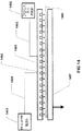
開示された方法の所与の実施形態では、ウェブ又は基板が、1又は複数のフィルム堆積用ソースを通過するように移動させられる。その場合、フィルム成長速度及び/又はイオン衝撃は、ソース内で又はソースからソースへと、基本的に基板の移動に平行な方向に変化する。これにより、衝撃パワー密度対成長速度の比率が、フィルムの厚さ方向において一定ではなくなる。所与の実施形態では、この方向における位置の関数としてのフィルムイオン衝撃パワー対成長速度の比率が、1又は複数の局所的な極小値を有してもよく、その場合、堆積速度は比較的大きい一方で衝撃は増加しないか又は減少してもよい。このような多層フィルムは、所与の実施形態では、1又は複数の線形プラズマソースから堆積させることができ、その場合、基板の移動方向は、1又は複数のソースの長手方向に対してほぼ垂直である。このような堆積システムにおいて、フィルムは、基板がソースを通過するにつれて成長速度が変わるように成長してもよい。さらに、ソース内に、イオン衝撃パワーも位置の関数として変化させるような構造があってもよい。所与の実施形態では、イオン衝撃のための独立したかつ別個に制御可能な電源があってもよく、堆積ガスの流量と速度を一定としながら基板の移動方向に沿ってイオン衝撃を変化させることができる。それにより、所望する方式でフィルム特性をフィルム厚さ方向に変化させることができる。 In a given embodiment of the disclosed method, the web or substrate is moved past one or more film deposition sources. In that case, the film growth rate and / or ion bombardment changes within the source or from source to source, essentially in a direction parallel to the movement of the substrate. Thereby, the ratio of the impact power density to the growth rate is not constant in the film thickness direction. In a given embodiment, the ratio of film ion bombardment power to growth rate as a function of position in this direction may have one or more local minima, in which case the deposition rate is relatively While large, the impact may not increase or decrease. Such multilayer films can be deposited from one or more linear plasma sources in a given embodiment, in which case the direction of movement of the substrate is substantially perpendicular to the longitudinal direction of the one or more sources. It is. In such a deposition system, the film may be grown such that the growth rate changes as the substrate passes through the source. Furthermore, there may be a structure in the source that also changes the ion bombardment power as a function of position. In a given embodiment, there may be an independent and separately controllable power source for ion bombardment that varies the ion bombardment along the direction of substrate movement while keeping the deposition gas flow rate and velocity constant. Can do. Thereby, the film characteristics can be changed in the film thickness direction in a desired manner.
OLED等の非常に繊細な材料については、バリアが堆積されることになる表面の上に不可避的に粒子が存在する。それらの粒子は、多くの場合、現状のバリア堆積方法ではリークスポットの原因となる。これは特に、プラスチックフィルム等のフレキシブル基板で云えることであり、これらの粒子は、撓み後のハーメチックコーティングに微細クラックを生じさせる。開示された方法は、基板が撓んだり伸張されたりしたときのコーティング内の全ての層の撓みや伸びに対する耐性をもったコーティング構造によって、温度の問題を克服する。さらに、この方法は、一連のステップを採用することにより最初から存在する表面粒子による欠陥を回避することができる。それは、ハーメチックバリア層としての新規の多層堆積構造の形成を含むものである。 For very delicate materials such as OLEDs, particles inevitably exist on the surface on which the barrier is to be deposited. These particles often cause leak spots in current barrier deposition methods. This is especially true for flexible substrates such as plastic films, where these particles cause microcracks in the hermetic coating after bending. The disclosed method overcomes the temperature problem with a coating structure that is resistant to deflection and elongation of all layers in the coating when the substrate is deflected or stretched. Furthermore, this method can avoid defects due to surface particles existing from the beginning by adopting a series of steps. It involves the formation of a novel multi-layer deposited structure as a hermetic barrier layer.
本発明の特定の実施形態では、多層であるコーティングが堆積され、ほとんど又は全体がケイ素ベースの誘電体材料から構成される。所与の実施形態では、その多層は、各層が約200nmより薄い透明材料でもよく、その場合、多層を構成する複数の元素は同じであるが、各元素の比率を僅かだけ変えてもよく、少なくとも第1のタイプの層(タイプ1)から少なくとも1つの他のタイプの層(タイプ2)へと変えてもよい。光学特性(屈折率及び光吸収)、透過率、硬度、弾性係数、内在応力及び/又は他の機械的特性等の他のフィルム特性も、1つのタイプの層から別のタイプの層へと、組成の場合よりも大きく変えてもよい。特定の本発明の実施形態では、3又はそれ以上のこのような層タイプ(タイプ1、...タイプn)があってもよく、それらは1つのタイプから別のタイプに組成が僅かだけ変わるようにしてもよい。
所与の実施形態では、コーティング内にそれらの2又はそれ以上のタイプの層以外に1又は複数の層があってもよく、それらは組成をより大きく変えてもよいが、共通の1又は複数の元素を有してもよい。所与の実施形態では、1又は複数の薄層(約20nmまでの厚さ)があってもよく、その薄層は、直前の層で堆積されたばかりの材料から形成されてもよい。その直前の層は、イオン衝撃又は化学修飾を含む堆積後処理を施されており、それらの処理は、表面にナノスケール又はミクロスケールの滑らかさを付与するか、又は、表面での透過率及び/又は化学的安定性を修飾するためのものである。
所与の実施形態では、パルス状プラズマにより層が堆積されてもよく、その場合、RF及び/又はVHF電力を100サイクルから20キロサイクルのパルス周波数でパルス化することができる。所与の実施形態では、少なくとも2つのタイプのうちのタイプ1層材料が厚さ2nmから50nmであり、かつ、タイプ2又は他の層の材料よりも低透過性とすることができる。低透過性層材料は、特定の実施形態では、負の内在応力が比較的大きい(圧縮力が大きく引張力が小さい)。所与の実施形態では、その層材料は、他の幾つかの層の材料よりも緻密で硬い。低透過性タイプの層は、イオン衝撃パワー密度対フィルム成長速度の比率を、タイプ2又は他の層材料よりも大きくなるようにして堆積させることができる。
堆積後に施された表面処理は、イオン衝撃により第1、第2又は他のタイプの層をさらに圧縮した非常に薄いサブ層を形成することができる。より高透過性の第2のタイプ又は他の層材料は、タイプ1層材料ほど硬くなくてもよい。タイプ2又は他の層材料は、厚さが約5nmから200nm程度であってもよい。タイプ1に比べて水分に対する透過性が(桁違いに)高いその層材料は、有機ポリマー又はプラスチックに比べればなお透過性が(桁違いに)遥かに低い。所与の実施形態では、高透過性の第2のタイプの層は、イオン衝撃パワー密度対成長速度の比率をより低くして堆積させることができ、よって堆積されたフィルムの各分子単層は、第1のタイプの層材料の分子単層に比べて少ないイオン衝撃エネルギーを受けたことになる。さらに、所与の実施形態では、低透過性の層材料は、圧縮力である内在応力を有しかつその絶対値は約50MPaより大きく、そして高透過性の層材料は、引張力又は−100MPa未満の圧縮力である内在応力を有することができる。
In certain embodiments of the invention, a coating that is multi-layered is deposited and is composed mostly or entirely of a silicon-based dielectric material. In a given embodiment, the multilayer may be a transparent material where each layer is thinner than about 200 nm, in which case the elements that make up the multilayer are the same, but the ratio of each element may vary slightly, There may be a change from at least a first type of layer (type 1) to at least one other type of layer (type 2). Other film properties such as optical properties (refractive index and light absorption), transmittance, hardness, elastic modulus, intrinsic stress and / or other mechanical properties can also be transferred from one type of layer to another type of layer, You may change large rather than the case of a composition. In certain embodiments of the present invention, there may be three or more such layer types (type 1, ... type n), which vary slightly in composition from one type to another. You may do it.
In a given embodiment, there may be one or more layers in the coating in addition to those two or more types of layers, which may change composition more greatly, but the common one or more You may have the element of. In a given embodiment, there may be one or more thin layers (thickness up to about 20 nm), which may be formed from the material just deposited in the previous layer. The immediately preceding layer has been subjected to post-deposition treatments that include ion bombardment or chemical modification, which can impart nanoscale or microscale smoothness to the surface, or the surface transmittance and And / or to modify chemical stability.
In a given embodiment, the layer may be deposited by a pulsed plasma, in which case RF and / or VHF power can be pulsed at a pulse frequency of 100 to 20 kilocycles. In a given embodiment, the type 1 layer material of at least two types may be 2 nm to 50 nm thick and may be less permeable than the type 2 or other layer material. The low permeability layer material, in certain embodiments, has a relatively high negative intrinsic stress (high compressive force and low tensile force). In a given embodiment, the layer material is denser and harder than the materials of several other layers. Low permeability type layers can be deposited such that the ratio of ion bombardment power density to film growth rate is greater than Type 2 or other layer materials.
Surface treatments applied after deposition can form very thin sub-layers that further compress the first, second or other types of layers by ion bombardment. The more permeable second type or other layer material may not be as stiff as the type 1 layer material. Type 2 or other layer material may have a thickness on the order of about 5 nm to 200 nm. Its layer material, which is highly permeable to moisture compared to type 1, is still much less permeable (by order of magnitude) than organic polymers or plastics. In a given embodiment, a highly permeable second type layer can be deposited with a lower ratio of ion bombardment power density to growth rate so that each molecular monolayer of the deposited film is As compared with the molecular monolayer of the first type layer material, the ion bombardment energy is less. Further, in a given embodiment, the low permeability layer material has an intrinsic stress that is a compressive force and its absolute value is greater than about 50 MPa, and the high permeability layer material is a tensile force or −100 MPa. It can have an intrinsic stress that is less than a compressive force.
フィルムが酸窒化ケイ素である本発明の特定の実施形態では、低透過性層材料が、高透過性層材料に比べて、より大きな弾性係数、より高い硬度、より大きい圧縮力である内在応力、及び、より小さい屈折率を有することができる。弾性係数、硬度、内在応力、酸素濃度、及び屈折率は、低透過性層材料内で変化させることもできる。所与の実施形態では、酸素濃度及び屈折率を、高透過性層材料においてより大きくすることができる。フィルムが実質的に窒化ケイ素である所与の実施形態では、低透過性層材料が、より大きな弾性係数と硬度、より小さい屈折率、より大きな窒素濃度、及びより大きな圧縮力である内在応力を有することができる。所与の実施形態では、高透過性層材料が、より小さい弾性係数と硬度、より小さい圧縮力である内在応力、より大きい屈折率、及び、異なる窒素及び/又は酸素の濃度を有してもよい。第1のタイプの材料から第2のタイプの材料への特徴的な機械的特性の変化は、100%を超えてもよいが、光学的特性及び元素組成は、約20%までの範囲内で変化させる。 In certain embodiments of the invention in which the film is silicon oxynitride, the low permeability layer material has a higher modulus of elasticity, higher hardness, intrinsic stress that is greater compressive force than the high permeability layer material, And can have a lower refractive index. Elastic modulus, hardness, intrinsic stress, oxygen concentration, and refractive index can also be varied within the low permeability layer material. In a given embodiment, the oxygen concentration and refractive index can be greater in the highly permeable layer material. In a given embodiment where the film is substantially silicon nitride, the low permeability layer material has a higher elastic modulus and hardness, a lower refractive index, a higher nitrogen concentration, and an intrinsic stress that is a higher compressive force. Can have. In a given embodiment, the highly permeable layer material may have a lower elastic modulus and hardness, a lower intrinsic compressive stress, a higher refractive index, and a different nitrogen and / or oxygen concentration. Good. The characteristic mechanical property change from the first type of material to the second type of material may exceed 100%, but the optical properties and elemental composition are within the range of up to about 20%. Change.
本発明の特定の実施形態では、イオン衝撃パワー密度対堆積速度の比率を変化させることにより、光学特性及び機械的特性を、1つの層の厚さ方向において、又は、堆積されたフィルムの1つの層グループ内で連続的に変化させることができる。このイオン衝撃パワー密度対堆積速度の比率は、1つの層内で、又は、層から層へと周期的に変化させることができる。タイプ1とタイプ2が交互になっており隣り合う層に最大と最小があり、各々が局所的な極大又は極小を有する所与の実施形態では、それにより得られる光学的特性及び機械的特性が、層グループの厚さ方向に同様の周期性を有している。このような変化は、3又はそれ以上の層タイプについて極大と極小が交互になっているものでもよい。その変化は、イオン衝撃対成長速度の比率同士の間又はそれらの比率の外側であるほぼ等しい堆積厚さを伴う準周期的なものでもよい。その変化は、屈折率(RI)又は機械的特性の高い領域と低い領域が幾つか交互になっている、周期的でもなく繰り返しでもないものでもよい。この場合、フィルムの組成もまた、フィルムの厚さ方向に僅かだけ変化してもよいが、実質的には同じ材料のままとする。フィルムの厚さ方向に変化する機械的特性は、硬度及び弾性係数における同様の変化を含んでもよい。 In certain embodiments of the invention, by varying the ratio of ion bombardment power density to deposition rate, optical and mechanical properties can be achieved in the thickness direction of one layer or one of the deposited films. It can be varied continuously within the layer group. This ratio of ion bombardment power density to deposition rate can be varied within a layer or periodically from layer to layer. In a given embodiment where Type 1 and Type 2 are alternating and there are maximum and minimum adjacent layers, each with local maxima or minima, the resulting optical and mechanical properties are The layer group has the same periodicity in the thickness direction. Such changes may be alternating maximum and minimum for three or more layer types. The change may be quasi-periodic with approximately equal deposition thickness that is between or outside the ratios of ion bombardment to growth rate. The change may be non-periodic or non-repetitive, with several alternating regions of high and low refractive index (RI) or mechanical properties. In this case, the composition of the film may also vary slightly in the thickness direction of the film, but remains substantially the same material. Mechanical properties that vary in the thickness direction of the film may include similar changes in hardness and elastic modulus.
本発明の実施形態では、1又は複数の層グループの堆積後に表面処理を行ってもよい。表面処理は、タイプ1若しくはタイプ2又は他の材料に対して行える。表面処理は、それらの層のいずれかの堆積に用いたプラズマソースとは設計の異なるプラズマソース中で比較的低い処理圧力下で行うことができる。 In embodiments of the present invention, surface treatment may be performed after the deposition of one or more layer groups. Surface treatment can be performed on Type 1 or Type 2 or other materials. The surface treatment can be performed at a relatively low processing pressure in a plasma source of a different design than the plasma source used to deposit any of those layers.
本発明の実施形態の多層コーティングは、極めて多様な異なるプラズマベース堆積システムで堆積されてもよく、それらは大型基板を処理可能なものである。所与の実施形態では、多層コーティングは、実質的に同じガスを供給されるが、堆積速度及び/又はイオン衝撃パワー密度が基板移動方向に沿って空間的に変化する複数のプラズマソースから移動基板上に堆積することができる。所与の実施形態では、多層構造を複数のソースにより静止基板上に堆積させることができる。その場合、ソースパワー若しくはガス混合物のいずれか、又は、ソースパワー及びガス混合物の双方を時間的にほぼ段階的方式で変化させることにより一層ずつ堆積されていき、そして堆積速度若しくはイオン衝撃パワー又はそれらの双方が層から層へと変化する。さらに、イオン衝撃パワー密度若しくは堆積速度又はそれらの双方において、層と層の間での急激な変化を伴うか、又は、層と層の間での遷移の限界厚さによる層特性変化の所与の長さ範囲を伴って、交互方式にて多層を堆積させることができる。高透過性又は抵透過性の層材料は、互いに組成において約20%を超えるほど異なってはならない。 The multilayer coatings of embodiments of the present invention may be deposited with a wide variety of different plasma-based deposition systems, which are capable of processing large substrates. In a given embodiment, the multilayer coating is supplied with substantially the same gas, but from multiple plasma sources where the deposition rate and / or ion bombardment power density varies spatially along the direction of substrate movement. Can be deposited on top. In a given embodiment, a multilayer structure can be deposited on a stationary substrate by multiple sources. In that case, either the source power or the gas mixture, or both the source power and the gas mixture, are deposited one by one by changing the source power and the gas mixture in a stepwise manner in time, and the deposition rate or ion bombardment power or those Both change from layer to layer. Further, given the bombardment of the layer properties due to the critical thickness of the transition between layers, with abrupt changes between layers, in ion bombardment power density or deposition rate or both. Multiple layers can be deposited in an alternating fashion with a length range of. Highly permeable or impermeable layer materials should not differ from each other by more than about 20% in composition.
イオン衝撃パワー密度対フィルム成長速度の比率が、プラズマ堆積フィルムにおける密度、ミクロ構造及び応力を決定する要因であり、そのフィルムの組成はそれほど重要ではないことは周知である。従って、イオン衝撃パワー密度対フィルム堆積速度の比率を変えることにより、幾つかの層と他の層の間に、透過性及び機械的特性における変化を生じる。所与の実施形態では、衝撃及び成長速度が一定であるか又は多層バルクを堆積する間にゆっくりと変化し、基板上での堆積速度又はイオン衝撃のいずれかが層と層の間の界面で急激に変化することにより分離される場合、堆積されるフィルムは、ほぼ一定の特性を有する多層と、それらの層と層の間にフィルム特性が遷移する非常に薄いバンドがある。所与の実施形態では、イオン衝撃パワー密度対成長速度の比率の変化、及び/又は、ガス混合物の変化により、上述した通り、任意のタイプ1層からそのフィルムが隣接しているタイプ2層へと、フィルムの元素組成が20%まで変化してもよい。 It is well known that the ratio of ion bombardment power density to film growth rate is a factor that determines density, microstructure and stress in plasma deposited films, and the composition of the film is not very important. Thus, changing the ratio of ion bombardment power density to film deposition rate causes changes in permeability and mechanical properties between some layers and others. In a given embodiment, the bombardment and growth rates are constant or change slowly during the deposition of the multilayer bulk, and either the deposition rate or ion bombardment on the substrate is at the interface between layers. When separated by abrupt changes, the deposited film has multiple layers with nearly constant properties and very thin bands where the film properties transition between the layers. In a given embodiment, a change in the ratio of ion bombardment power density to growth rate, and / or a change in the gas mixture, as described above, from any type 1 layer to a type 2 layer to which the film is adjacent. And the elemental composition of the film may vary up to 20%.
特定の実施形態では、層から層への特性の変化は、おおよそ段階的方式で組成を変えることにより、又は、ガス混合物の成分比を変えることにより実現してもよい。所与の実施形態では、コーティングが窒化ケイ素又は酸窒化ケイ素の材料でもよく、その場合、窒素の濃度及び/又はケイ素窒素結合密度は、1つの層から隣の層へ緩やかな割合で変化し、そして水分透過率は、より多く窒素を含むタイプの層とより窒素濃度の低いタイプの層とでは異なる。所与の実施形態では、窒素濃度が変化する多層が、密度、硬度、弾性係数及びミクロ構造においても変化してもよい。 In certain embodiments, the change in properties from layer to layer may be achieved by changing the composition in an approximately step-wise fashion, or by changing the component ratio of the gas mixture. In a given embodiment, the coating may be a silicon nitride or silicon oxynitride material, in which case the nitrogen concentration and / or silicon nitrogen bond density varies at a gradual rate from one layer to the next, The moisture permeability is different between a layer containing more nitrogen and a layer having a lower nitrogen concentration. In a given embodiment, the multilayer with varying nitrogen concentration may also vary in density, hardness, modulus of elasticity and microstructure.
所与の実施形態では、このフレキシブルコーティング構造を、基板をプラズマの近傍に配置し、コーティングプロセスを行うときにプラズマからイオン衝撃を生じさせることにより形成することができる。所与の実施形態では、フィルム形成の方法が、プラズマ増強又はプラズマ支援化学気相蒸着(PACVD又はPECVD)である。開示されたバリアのために格段に向上したフレキシビリティは、一部にはその多層構造からくるものである。この多層化は、微細クラックの進行を阻止し、開示されたコーティングにおける撓みに対する耐性を単層フィルムに比べて格段に向上させる。これは1つには層と層の間の剪断歪みに対する耐性が向上することによる。これは、若干"板"バネ構造に似ている。さらに、よりソフトな層は、汎用的なすなわりバルクの窒化ケイ素に比べて実質的に弾性係数が低いので、弾性的にはより"伸び"易い。 In a given embodiment, the flexible coating structure can be formed by placing the substrate in the vicinity of the plasma and causing ion bombardment from the plasma when performing the coating process. In a given embodiment, the method of film formation is plasma enhanced or plasma assisted chemical vapor deposition (PACVD or PECVD). The greatly improved flexibility due to the disclosed barrier is partly due to its multilayer structure. This multilayering prevents the progression of microcracks and significantly improves the resistance to bending in the disclosed coating compared to single layer films. This is due in part to improved resistance to shear strain between layers. This is somewhat similar to a “plate” spring structure. In addition, the softer layer is elastically easier to “elongate” because it has a substantially lower elastic modulus than the generic, ie, bulk silicon nitride.
本発明のコーティング方法の特定の実施形態では、イオン衝撃パワー密度対成長速度の比率が、タイプ2材料(A)に対する下値とタイプ1材料(B)に対する上値との間で略段階的に変化してもよく、少なくともコーティングABABABAの部分を含む。所与の実施形態では、その比率は複数の範囲内、X1<R1<X2;Y1<R1<Y2;Z1<R3<Z2の値でもよく、各範囲はフィルム層の単一のタイプを構成する。材料の層タイプが2つより多い場合、第3のタイプ(C)の材料がある場合、周期的なACBCACBCA、ACBACBACB、ACACBCBC等のシーケンス若しくは他の材料層シーケンスとすることができ、又は、より複雑な若しくはACBCBCAC等の非周期的なシーケンスとすることができる。所与の実施形態では、3つのこのようなタイプの層を交互に堆積させることができる。 In a particular embodiment of the coating method of the present invention, the ratio of ion bombardment power density to growth rate varies approximately stepwise between a lower value for Type 2 material (A) and an upper value for Type 1 material (B). It may include at least a portion of the coating ABABABA. In a given embodiment, the ratio may be within a plurality of ranges, X 1 <R 1 <X 2 ; Y 1 <R 1 <Y 2 ; Z 1 <R 3 <Z 2 , each range being a film Configure a single type of layer. If there are more than two layer types of material, if there is a third type (C) material, it can be a periodic ACBCCACBCA, ACBACBACB, ACACBCBC, or other material layer sequence, or more It can be a complex or non-periodic sequence such as ACBCBCAC. In a given embodiment, three such types of layers can be deposited alternately.
本発明の特定の実施形態では、1つの層から隣の層へのフィルム特性の遷移を急激な変化とすることができ、遷移厚さを隣の層の厚さの約50%までとすることができる。所与の実施形態では、フィルムの瞬間的成長速度をフィルム方向において段階的に変化させる一方、イオン衝撃パワー密度は比較的小さく変化することにより、上述したように層特性を層から層へと変化させることができる。所与の実施形態では、層から層へのフィルム特性の変化を、プラズマに噴射されるガス混合物の異なる反応物質又はプリカーサガスの濃度を僅かに変えることにより得ることができる。インラインシステム等の、多層構造を形成するためのシステムの所与の実施形態では、異なる層の堆積材料が、単一のプラズマソースの中に同時に得られてもよく、その場合、イオン衝撃パワー密度は、フィルムが成長している基板領域に亘って僅かだけ変化するか、全く変化しないが、堆積速度は基板移動方向に沿ってより大きく変化する。 In certain embodiments of the invention, the film property transition from one layer to the next can be abrupt and the transition thickness can be up to about 50% of the thickness of the next layer. Can do. In a given embodiment, the instantaneous growth rate of the film is changed stepwise in the film direction while the ion bombardment power density is changed relatively small to change the layer properties from layer to layer as described above. Can be made. In a given embodiment, the change in film properties from layer to layer can be obtained by slightly varying the concentration of different reactants or precursor gases in the gas mixture injected into the plasma. In a given embodiment of a system for forming a multilayer structure, such as an in-line system, different layers of deposition material may be obtained simultaneously in a single plasma source, in which case the ion bombardment power density Varies slightly or not at all over the substrate area on which the film is growing, but the deposition rate varies more along the direction of substrate movement.
本発明の特定の実施形態では、成長速度に対するイオン衝撃パワー密度を増加又は減少させるために、イオン衝撃パワー密度対成長速度の比率の変化を、アルゴン等の不活性ガスの流量割合を変えることにより、又は、プラズマソースのガス圧力を変えることにより実現することができる。層から層への堆積材料のタイプの変化によって、カプセル構造と組成が得られ、その場合、少なくとも1つのタイプの層がより硬くかつ/又はより緻密な材料であってそれにおける水分透過はより強力に阻止される一方、1又は複数のタイプの層はより柔軟であるため、それらのソフト層は、大きな撓みを許容する基板の弾性変形に対してより大きな耐性を有する。所与の実施形態では、それらの層は、低透過層対高透過層の厚さの比が約1:20から約3:1となるように構成されてもよい。通常、低透過タイプの層は高透過タイプの層よりもあまり厚くならないように構成されるが、高透過タイプの層は低透過タイプの層よりもかなり厚くてもよい。 In certain embodiments of the invention, the ratio of ion bombardment power density to growth rate is varied by changing the flow rate of an inert gas such as argon in order to increase or decrease the ion bombardment power density relative to the growth rate. Alternatively, it can be realized by changing the gas pressure of the plasma source. The change in the type of deposited material from layer to layer results in a capsule structure and composition, in which case at least one type of layer is a harder and / or denser material, in which moisture transmission is stronger. While one or more types of layers are more flexible, their soft layers are more resistant to elastic deformation of the substrate that allows greater deflection. In a given embodiment, the layers may be configured such that the ratio of the thickness of the low transmission layer to the high transmission layer is from about 1:20 to about 3: 1. Typically, the low transmission type layer is configured to be less thick than the high transmission type layer, but the high transmission type layer may be much thicker than the low transmission type layer.
本発明の特定の実施形態では、コーティングプロセス中、移動方向に沿った位置の関数としてのイオン衝撃パワー密度対フィルム成長速度の比率が、1又は複数の極小値を有し、そこでは堆積速度は大きいが、イオン衝撃は増加しないか又は減少することもある。このようなプロセスは、所与の実施形態では、ほぼ平行に配置された1又は複数の長い線形プラズマソース(プラズマ源)を有するシステムにより行われ、その場合、基板の移動方向は、ソースの長手方向にほぼ垂直である。開示された方法の所与の実施形態では、ウェブ又は基板が、フィルム堆積のために1又は複数のソースを通過するように連続的に又は段階的に移動し、その場合、堆積速度及び/又はイオン衝撃パワー密度が、基本的に基板移動方向において1つのソースの中で、又は、ソースからソースへと変化させることができる。これにより、衝撃パワー密度対成長速度の比率が、コーティングされる基板上のいずれのポイントにおいても時間的に変化し、従って、ここに開示したようにフィルムの厚さ方向に層形成されることになる。所与の実施形態では、ソースが、イオン衝撃パワーを位置の関数として変化させるような構造を有し、これは、電極上の電圧を変えることにより、又は、電極の部品若しくは個別の電極から基板までの間隙を変えることによるものでもよい。所与の実施形態では、独立しかつ別々に制御可能なイオン衝撃のための電源、例えば、基板の下の電極等があってもよく、そのパワー密度を基板移動方向に沿って変化させることができる。そのとき堆積ガスが流れていてもよくかつ速度は変化しないか又は僅かだけ変化してもよく、それによりフィルム特性が、所望する方式でフィルムの厚さ方向に変化する。 In certain embodiments of the invention, during the coating process, the ratio of ion bombardment power density to film growth rate as a function of position along the direction of travel has one or more local minimum values, where the deposition rate is Although large, ion bombardment may not increase or decrease. Such a process is performed in a given embodiment by a system having one or more long linear plasma sources (plasma sources) arranged substantially parallel, in which case the direction of movement of the substrate is the length of the source It is almost perpendicular to the direction. In a given embodiment of the disclosed method, the web or substrate is moved continuously or stepwise through one or more sources for film deposition, where the deposition rate and / or The ion bombardment power density can basically be varied in one source or from source to source in the direction of substrate movement. This causes the ratio of impact power density to growth rate to change over time at any point on the substrate to be coated and thus be layered in the thickness direction of the film as disclosed herein. Become. In a given embodiment, the source has a structure that changes the ion bombardment power as a function of position, which can be achieved by changing the voltage on the electrode or from a component of the electrode or from an individual electrode. It may be by changing the gap until. In a given embodiment, there may be an independent and separately controllable power source for ion bombardment, such as an electrode under the substrate, which can vary its power density along the direction of substrate movement. it can. The deposition gas may then flow and the velocity may not change or may change only slightly, thereby changing the film properties in the thickness direction of the film in the desired manner.
上記のいずれかの用途のためのOLED又はPVのいずれかのコーティングプロセスは、所与の実施形態では、以下に挙げるプロセスステップの様々な組合せを含むものである。通常、超清浄又は無欠陥コーティングが要求される用途は、さらなるクリーニングと表面調整ステップを必要とし、カプセル化において多層による利点を享受する。ハーメチックカプセル化を行わない、光学コーティング等の欠陥をあまり気にしないコーティング用途は、表面クリーニングステップはより少ないか全く無くてもよいが、堆積ステップでは層厚さをより制御することが必要である。所与の実施形態では、基板の温度を約150℃未満とすることができる。さらに、OLEDベース製品製造では、ほとんどの場合、プロセス中の温度は約85℃未満とすべきである。例えば、有機PV(OPV)のカプセル化に使用される実施形態では、プロセス時間の大部分で基板温度は約100℃未満に維持すべきであり、この温度を超えるのはほんの僅かな時間かつ僅かな温度のみとすべきである。CIGSのカプセル化は、通常、120℃未満の温度とすることができる。 The coating process of either OLED or PV for any of the above applications, in a given embodiment, involves various combinations of the process steps listed below. Usually, applications that require ultra-clean or defect-free coatings require additional cleaning and surface conditioning steps and enjoy the advantages of multiple layers in encapsulation. Coating applications that do not perform hermetic encapsulation and are less sensitive to defects such as optical coatings may require fewer or no surface cleaning steps, but the deposition step requires more control over the layer thickness. . In a given embodiment, the temperature of the substrate can be less than about 150 degrees Celsius. Further, in most OLED-based product manufacturing, the temperature during the process should be less than about 85 ° C. For example, in an embodiment used for encapsulation of organic PV (OPV), the substrate temperature should be maintained below about 100 ° C. for most of the process time, exceeding this temperature for only a short time and It should be only the correct temperature. CIGS encapsulation can typically be at temperatures below 120 ° C.
特定の実施形態では、タイプ2層の硬度が約4ギガパスカル(GPa)を超えればよい一方、タイプ1層の硬度は20GPa程度とすることができる。双方のタイプを含むコーティングの全厚さの平均硬度は、約5GPaと約12GPaの間でよい。(通常、約150℃と400℃の間の温度で堆積される汎用的なプラズマ堆積窒化ケイ素の硬度は、約10GPaから約22GPaの間にできる一方、通常1100℃までの温度で堆積される熱蒸着又はバルク焼結された窒化ケイ素は約30GPaまでの硬度を有することができる。)従って、開示されたフレキシブルコーティングの硬度は、焼結又は熱蒸着された窒化ケイ素のそれに比べてかなり低いが、水分透過に対する大きな耐性を保持している。所与の実施形態では、層中のタイプ2材料の厚さは、層中のタイプ1材料の厚さよりも大きくてもよく、それにより厚さ平均した多層コーティング硬度は、ハードな層の硬度よりもソフトな層の硬度に近いものとなる。所与の好適な実施形態では、タイプ1層の硬度は約8GPaと約16GPaの間でよく、タイプ2層の硬度は約5GPaと約10GPaの間でよい。 In certain embodiments, the hardness of the Type 1 layer may be about 20 GPa while the hardness of the Type 2 layer may exceed about 4 gigapascals (GPa). The average hardness of the total thickness of the coating, including both types, can be between about 5 GPa and about 12 GPa. (Typically, the hardness of general purpose plasma deposited silicon nitride deposited at temperatures between about 150 ° C. and 400 ° C. can be between about 10 GPa and about 22 GPa, while heat deposited at temperatures typically up to 1100 ° C. Vapor deposited or bulk sintered silicon nitride can have a hardness of up to about 30 GPa.) Thus, the hardness of the disclosed flexible coating is significantly lower than that of sintered or thermally vapor deposited silicon nitride, Maintains great resistance to moisture permeation. In a given embodiment, the thickness of the type 2 material in the layer may be greater than the thickness of the type 1 material in the layer, so that the thickness averaged multilayer coating hardness is greater than the hardness of the hard layer. Is close to the hardness of the soft layer. In a given preferred embodiment, the hardness of the type 1 layer may be between about 8 GPa and about 16 GPa, and the hardness of the type 2 layer may be between about 5 GPa and about 10 GPa.
所与の実施形態では、開示されたコーティング構造における材料の弾性係数が、約40GPaから約240GPaまでの範囲で変化し、コーティングの厚さ平均は約60GPaと160GPaの間となる。これは、ナノ−インデンテイションを用い、スタイラスの弾性の影響を補償することにより計測することができる。層中のタイプ2層の弾性係数は約40GPaから約130GPaまでの範囲とすることができ、一方、層中のタイプ1層の弾性係数は約80GPaから約240GPaまでの範囲とすることができる。特定の実施形態では、層中のタイプ2層の弾性係数(ヤング率)は約55GPaから約110GPaまでの範囲とすることができ、一方、層中のタイプ1層の弾性係数は約90GPaから約180GPaまでの範囲とすることができる。焼結されかつ高温で成長した窒化ケイ素における通常の弾性係数は、一般的に約250GPaと約300GPaの間であり、一方、低温(150℃〜400℃)プラズマ堆積された窒化ケイ素の弾性係数は、一般的に約110GPaと200GPaの間である。従って、開示された窒化ケイ素又は酸窒化ケイ素の多層フィルムは、個々の層の弾性係数においても平均な弾性係数においても、高温若しくは焼結による窒化ケイ素又は高温プラズマ堆積された窒化ケイ素に比べて弾性限界範囲内で圧縮や伸張が若干容易である。タイプ1フィルム層の内在応力は−50MPa(圧縮力)と−500MPa(圧縮力)の間の範囲とすることができ、一方、タイプ2層の内在応力は−100MPa(圧縮力)と+200MPa(引張力)の間の範囲とすることができる。コーティングの結合層は、約−200MPa(圧縮力)と約50MPa(引張力)の間の組み合わされた内在応力を有することができる。 In a given embodiment, the elastic modulus of the material in the disclosed coating structure varies from about 40 GPa to about 240 GPa, and the coating thickness average is between about 60 GPa and 160 GPa. This can be measured by using nano-indentation and compensating for the effects of stylus elasticity. The elastic modulus of the type 2 layer in the layer can range from about 40 GPa to about 130 GPa, while the elastic modulus of the type 1 layer in the layer can range from about 80 GPa to about 240 GPa. In certain embodiments, the elastic modulus (Young's modulus) of the type 2 layer in the layer can range from about 55 GPa to about 110 GPa, while the elastic modulus of the type 1 layer in the layer is from about 90 GPa to about The range can be up to 180 GPa. The usual elastic modulus in sintered and grown high temperature silicon nitride is typically between about 250 GPa and about 300 GPa, while the low modulus (150 ° C. to 400 ° C.) plasma deposited silicon nitride has an elastic modulus of Typically between about 110 GPa and 200 GPa. Thus, the disclosed silicon nitride or silicon oxynitride multilayer films are more elastic than either high temperature or sintered silicon nitride or high temperature plasma deposited silicon nitride, both in the elastic modulus and average elastic modulus of the individual layers. It is a little easier to compress and stretch within the limit range. The intrinsic stress of the type 1 film layer can be in the range between -50 MPa (compressive force) and -500 MPa (compressive force), while the intrinsic stress of the type 2 layer is -100 MPa (compressive force) and +200 MPa (tensile) Force). The tie layer of the coating can have a combined intrinsic stress between about -200 MPa (compressive force) and about 50 MPa (tensile force).
所与の実施形態では、タイプ1材料は、約10nm/分から約200nm/分の成長速度で堆積させることができ、一方、タイプ2材料は約20nm/分から約500nm/分の成長速度で堆積させることができる。このようなコーティングを形成するプロセスの所与の実施形態では、タイプ1材料及びタイプ2材料の双方におけるプラズマソースパワー密度(プラズマ領域と接触する基板+複数の電極+複数の導電壁の複数の組合せ領域により分割された複数の電極に対するRF+VHFの全電力)が約0.05ワット/cm2から約1ワット/cm2でよく、特定の実施形態では、約0.1ワット/cm2から約0.5ワット/cm2の範囲でよい。基板上のイオン衝撃パワー密度は、ソース平均プラズマパワー密度の約4分の1から約2倍の間とすることができる。ソース設計の所与の実施形態では、イオン衝撃パワーをプラズマの全パワーの大部分とすることができ、基板上のイオン衝撃パワー密度を電極上のそれよりも大きくすることができる。所与の実施形態では、イオン衝撃パワー密度はほぼ同程度でも、タイプ1層をタイプ2層よりも遅い堆積速度で堆積させることができる。所与の実施形態では、ここで示したタイプ1及びタイプ2の双方のタイプを、単一プラズマソースから同時に堆積させることができ、又は、隣接するプラズマソースにより同時に堆積させることができ、又は、同じプラズマソースにより別々の時間に堆積させることができる。 In a given embodiment, type 1 material can be deposited at a growth rate of about 10 nm / min to about 200 nm / min, while type 2 material is deposited at a growth rate of about 20 nm / min to about 500 nm / min. be able to. In a given embodiment of the process of forming such a coating, the plasma source power density in both type 1 and type 2 material (substrate in contact with plasma region + multiple electrodes + multiple combinations of conductive walls) RF + VHF total power for multiple electrodes divided by region) may be from about 0.05 watt / cm 2 to about 1 watt / cm 2 , and in certain embodiments, from about 0.1 watt / cm 2 to about 0 It may be in the range of 5 Watts / cm 2 . The ion bombardment power density on the substrate can be between about one quarter and about twice the source average plasma power density. In a given embodiment of the source design, the ion bombardment power can be the majority of the total power of the plasma, and the ion bombardment power density on the substrate can be greater than that on the electrode. In a given embodiment, a Type 1 layer can be deposited at a slower deposition rate than a Type 2 layer, even though the ion bombardment power density is approximately the same. In a given embodiment, both Type 1 and Type 2 types shown here can be deposited simultaneously from a single plasma source, or can be deposited simultaneously by adjacent plasma sources, or It can be deposited at different times by the same plasma source.
低透過性であるタイプ1層は、所与の実施形態では、2nmと30nmの間の厚さの透明材料とすることができ、フィルムを通る水分透過を阻止するために非透過性材料を設けるように堆積される。この層は、期間中連続的に堆積されても中断しながら堆積させることができ、その期間中、堆積される材料の任意の層内の機械的特性を変えるようにイオン衝撃パワー密度対堆積速度の比率を変化させることができる。タイプ1層内の硬度や弾性係数等の機械的特性の範囲は、一般的にタイプ2層内のそれらの特性の範囲とは重ならない。類似した組成の3又はそれ以上のタイプの層を有するコーティングについては、3番目又はそれよ以上のタイプの機械的特性の範囲は、タイプ1及びタイプ2の範囲と重なってもよい。 A type 1 layer that is low-permeability can be a transparent material with a thickness between 2 nm and 30 nm in a given embodiment, providing a non-permeable material to prevent moisture transmission through the film. So that it is deposited. This layer can be deposited continuously or interrupted during the period, during which time the ion bombardment power density versus the deposition rate to alter the mechanical properties in any layer of the deposited material. The ratio of can be changed. The range of mechanical properties such as hardness and elastic modulus within the type 1 layer generally does not overlap with the range of those properties within the type 2 layer. For coatings having three or more types of layers of similar composition, the third or more types of mechanical property ranges may overlap with the Type 1 and Type 2 ranges.
タイプ1層及びタイプ2層を有する、そして可能であれば他の材料層も有するコーティングで示した特定の実施形態では、2つのグループで堆積されてもよく、各グループがタイプ1層及びタイプ2層の双方を含む。第1及び第2のグループの層の堆積の間に表面処理があってもよく、その表面処理は、異なる材料の極薄層が得られる堆積を含んでも含まなくてもよい。所与の実施形態では、表面処理は高レベルのイオン衝撃を含むことにより、第1のグループの層の暴露された表面がイオン衝撃によりスパッタリングされて滑らかにされる。この第1のグループ内のタイプ2層はタイプ1層と交互になっている。それらの層の全厚さは、約20nmから2000nm程度までの範囲とすることができ、特定の実施形態では、約40nmと800nmの間とすることができる。そのグループの堆積に続いて、表面処理を行ってもよく、表面処理では、表面の10nm未満の範囲が材料の極薄層で置換されることにより、表面がマイクロスケール、ナノスケールで又は双方で、より滑らかになる。表面処理はイオン衝撃を含んでもよく、イオン衝撃では、表面材料のスパッタリングとともに表面トポロジーの平滑化が行われる。表面処理では、イオン衝撃又はこの処理の化学反応により極薄層の組成に多少の置換があってもよい。表面処理では、粒子や他の表面不規則要因による任意の突起から生じる粗さも低減できる。所与の実施形態では、このような極薄層は、そのグループのトップ層の上に堆積される、さらに別の極薄層とすることができる。その極薄層は、低速で堆積させることができるが、相当量のイオン衝撃パワー密度に曝されることにより、その極薄層の堆積前の表面に比べてその極薄層の表面はミクロスケール又はナノスケールでより滑らかになる。所与の実施形態では、その極薄層は、パルス状プラズマにより堆積させることができる。その極薄層の上に、タイプ2層及びタイプ1層を含む第2のグループの層が堆積される。タイプ2層及びタイプ1層は交互に堆積させることができ、又は所与の実施形態では、他の層を組み合わせることができる。上述したように、層グループの全厚さは、約100nmと約5000nmの間とすることができる。 In the particular embodiment shown with a coating having type 1 and type 2 layers, and possibly other material layers, it may be deposited in two groups, each group being type 1 and type 2 Includes both layers. There may be a surface treatment between the deposition of the first and second groups of layers, the surface treatment may or may not include a deposition that results in an ultra-thin layer of a different material. In a given embodiment, the surface treatment includes a high level of ion bombardment so that the exposed surface of the first group of layers is sputtered and smoothed by ion bombardment. Type 2 layers in this first group alternate with type 1 layers. The total thickness of these layers can range from about 20 nm to as much as 2000 nm, and in certain embodiments can be between about 40 nm and 800 nm. Subsequent to the deposition of the group, a surface treatment may be performed, where the surface is microscale, nanoscale or both by substituting an ultra-thin layer of material with a sub-10 nm area of the surface. , Get smoother. The surface treatment may include ion bombardment, in which surface topology is smoothed along with sputtering of the surface material. In the surface treatment, there may be some substitution in the composition of the ultrathin layer by ion bombardment or the chemical reaction of this treatment. Surface treatment can also reduce roughness resulting from any protrusions due to particles and other surface irregularities. In a given embodiment, such an ultrathin layer can be yet another ultrathin layer deposited over the top layer of the group. The ultrathin layer can be deposited at a slow rate, but exposure to a significant amount of ion bombardment power density causes the surface of the ultrathin layer to be microscale compared to the predeposition surface of the ultrathin layer. Or it becomes smoother at the nanoscale. In a given embodiment, the ultrathin layer can be deposited by a pulsed plasma. A second group of layers is deposited over the ultrathin layer, including Type 2 and Type 1 layers. Type 2 and type 1 layers can be deposited alternately, or in a given embodiment, other layers can be combined. As described above, the total thickness of the layer group can be between about 100 nm and about 5000 nm.
本発明の他の実施形態では、タイプ1層及びタイプ2層からなる、1又は複数のさらに別のグループが、最初のグループの上に堆積することができる。所与の実施形態では、各グループの最後の層の堆積後に行われる表面処理と共に3又はそれ以上のタイプの層が存在することができる。 In other embodiments of the invention, one or more further groups of type 1 and type 2 layers can be deposited over the first group. In a given embodiment, there can be three or more types of layers with surface treatments performed after deposition of the last layer of each group.
所与の実施形態では、タイプ1層及びタイプ2層のフィルム化学量論的組成における変化があってもよく、その場合、組み合わされた成分の濃度における変化が、組成物全体の約25%までである。所与の実施形態では、タイプ1層又はタイプ2層の機械的特性が、その後にどのような層グループがあるとしても、その厚さ内ではタイプ1層及びタイプ2層について特定された範囲内で変化させることができる。 In a given embodiment, there may be a change in the film stoichiometric composition of type 1 and type 2 layers, in which case the change in the concentration of the combined ingredients is up to about 25% of the total composition. It is. In a given embodiment, the mechanical properties of a type 1 layer or type 2 layer are within the range specified for the type 1 layer and type 2 layer within its thickness no matter what layer group it follows. Can be changed.
一例として、タイプ1層又はタイプ2層の組成が窒化ケイ素又は酸窒化ケイ素であり、その場合、ケイ素対窒素の比率が、少なくとも1つのタイプの層における最小約0.65から、少なくとも1つの他のタイプの層における最大1.0程度まで変化する。特定の実施形態では、窒化ケイ素におけるケイ素対窒素の濃度比が約0.65から0.8の間の範囲とすることができ、一方、酸窒化ケイ素においてはその範囲は0.7から1.0とすることができる。所与の実施形態では、炭素、酸素、及びフッ素のうち1又は複数の元素の、幾つかの層における濃度の僅かな混合又は変化として、層から層への材料組成の変化とすることができ、それらの全濃度は、全フィルムの20%又はそれ未満とすることができる。所与の実施形態では、タイプ2層又は他の高透過性の層は、プラスチック等の多くの他の材料に比べてなおかなり低透過性とすることができ、汎用的なプラズマ堆積された二酸化ケイ素に比べてさえ同等又は低透過性とすることができる。所与の実施形態では、この構造の所与の層が、少量のドーパントを有することができ、それらはホウ素、ヒ素、リン、イオウ並びに金属のうちの1又は複数を含むことができる。金属にはアルミニウム、亜鉛、スズ、インジウム及び銅等を含む。 As an example, the composition of the type 1 layer or type 2 layer is silicon nitride or silicon oxynitride, in which case the silicon to nitrogen ratio is at least one other from at least about 0.65 in at least one type of layer It varies up to about 1.0 in the type of layer. In certain embodiments, the silicon to nitrogen concentration ratio in silicon nitride can range between about 0.65 and 0.8, while in silicon oxynitride the range is 0.7 to 1. It can be set to zero. In a given embodiment, the change in material composition from layer to layer can be as a slight mixture or change in the concentration of one or more of carbon, oxygen, and fluorine in several layers. Their total concentration can be 20% or less of the total film. In a given embodiment, a type 2 layer or other highly permeable layer can still be much less permeable compared to many other materials such as plastics, and a universal plasma deposited dioxide dioxide. It can be equivalent or even less permeable than silicon. In a given embodiment, a given layer of this structure can have a small amount of dopant, which can include one or more of boron, arsenic, phosphorus, sulfur and metals. Metals include aluminum, zinc, tin, indium, copper and the like.
さらに、本発明の所与の実施形態では、異なるタイプの層の主成分(酸窒化ケイ素についてはシリコン及び窒素)が、1つの層から次の層へと25%未満で変化することができる。タイプ1及びタイプ2等の異なるタイプの層は、それらの界面で屈折率が僅かだけ異なる(628nmの波長で約0.20nm未満)ことにより、可視光がコーティングの多層の積層を実質的な内部の界面反射を生じずに通過する。 Furthermore, in a given embodiment of the invention, the major components of different types of layers (silicon and nitrogen for silicon oxynitride) can vary from one layer to the next in less than 25%. Different types of layers, such as Type 1 and Type 2, have a slightly different index of refraction at their interface (less than about 0.20 nm at a wavelength of 628 nm), so that visible light can substantially penetrate the multilayer stack of coatings. Passes without causing interface reflection.
<堆積プロセス及びコーティング構造>
本発明の所用の実施形態では、上記の開示された多層のいずれの堆積も、150℃未満の基板温度で行うことができる。多くのタイプのポリマー基板上での所与の用途においては、好適には基板温度は100℃未満である。OLEDデバイス等を搭載する繊細な基板における所与の実施形態では、基板温度80℃未満で行うことができる。そのような低い基板温度において、ある程度の堆積速度での酸化物、酸窒化物、又は窒化物の材料の堆積は、本明細書に包含された文献におけるように、電極対の間に反応物質ガスを噴射される線形プラズマソースを用いることにより実現することができる。所与の実施形態では、堆積及び表面処理プロセスは、平行プレート堆積システムすなわち高密度プラズマ堆積システムにて行うことができる。これらのフィルムについては、プリカーサガスが、1又は複数の以下のものを含むことができる。
a. 実質的に無機の酸化ケイ素又は酸窒化ケイ素を堆積するためのプリカーサ:シラン、ジシラン、メチルシラン、HMDSO、TEOS、TMCTS、BTBAS、VTMS、及びHMDS。(一般的に、有意な炭素を含有しない実質的に無機のフィルムを形成するためには、いずれかの有機ケイ素プリカーサ化合物と共に、20対1以上の大きな割合の反応物質が必要である。)
b. 炭素ドープされた酸化ケイ素又は酸窒化ケイ素を堆積するためのプリカーサ:[(シラン若しくはジシラン又は他のシラン)]と[(メタン若しくはエタン又はハイドロ炭素又はアルコール]。あるいは、単一プリカーサ:メチルシラン、HMDSO、TEOS、TMCTS、BTBAS、VTMS、及びHMDS。
c. 炭素ドープ材料とも称される、炭素ドープされたケイ素ベース酸化物又はケイ素ベース酸窒化物を堆積するためのプリカーサ(>5% 炭素はポリマー含有量の約5%を超える):HMDSO、TEOS、TMCTS、BTBAS、VTMS、及びHMDS。
d. 無機又は炭素ドープされた窒化ケイ素を堆積するためのプリカーサ:[(シラン、又は高次シラン若しくは環状ケイ素−水素化合物)と(メタン、エタン、直鎖若しくは環状炭化水素、又はアルコール)を含む組合せ]、メチルシラン、BTBAS、及びHMDS。(一般的に、有意な炭素を含有しない実質的に無機のフィルムを形成するためには、いずれかの有機ケイ素プリカーサ化合物と共に、20対1以上の大きな割合の酸化ガスの反応物質が必要である。)
e. ポリマー含有率が高い、炭素ドープされたケイ素ベース窒化物を堆積するためのプリカーサ:[(シラン、又は高次シラン若しくは環状ケイ素−水素化合物)と(メタン、エタン、直鎖若しくは環状炭化水素、又はアルコール)を含む組合せ]、メチルシラン及び高次シラン、BTBAS、並びにHMDS。
f. 無機又は炭素ドープされた金属酸化物及び金属酸窒化物を堆積するためのプリカーサ:トリメチルアルミニウム、ジメチル亜鉛、トリメチルインジウム、テトラメチルスズ、テトラキス(t−ブトキシ)ハフニウム、テトラキス(ジメチルアミノ)チタン及びその他、ビス(インデニル)ジメチルジルコニウム、トリス−n−シクロペンタジエニルイットリウム。一般的に、実質的に無機材料を形成するためには反応物質ガスの大きな流量比が必要である。
g. 多量に炭素ドープ(>10%)された金属酸化物及び金属酸窒化物を堆積するためのプリカーサ:トリメチルアルミニウム、ジメチル亜鉛、トリメチルインジウム、テトラメチルスズ、テトラキス(t−ブトキシ)ハフニウム、テトラキス(ジメチルアミノ)チタン及びその他、ビス(インデニル)ジメチルジルコニウム、トリス−n−シクロペンタジエニルイットリウム。上記のいずれにも[メタン、エタン、直鎖又は環状炭化水素、アルコール及び他の揮発性炭水化物]を追加してよい。
h. 無機又は炭素含有金属窒化物を堆積するためのプリカーサ:トリメチルアルミニウム、ジメチル亜鉛、トリメチルインジウム、テトラメチルスズ、テトラキス(t−ブトキシ)ハフニウム、テトラキス(ジメチルアミノ)チタン及びその他、ビス(インデニル)ジメチルジルコニウム、トリス−n−シクロペンタジエニルイットリウム。一般的に、有意の炭素を含まない実質的に無機のフィルムを形成するためには有機金属プリカーサ化合物のいずれかと共に、反応物質ガスの大きな流量比が必要である。
i. 炭素含有率が高い(>5%)、炭素ドープされた金属窒化物を堆積するためのプリカーサ:トリメチルアルミニウム、ジメチル亜鉛、トリメチルインジウム、テトラメチルスズ、テトラキス(t−ブトキシ)ハフニウム、テトラキス(ジメチルアミノ)チタン及びその他、ビス(インデニル)ジメチルジルコニウム、トリス−n−シクロペンタジエニルイットリウム。
<Deposition process and coating structure>
In certain embodiments of the invention, any of the disclosed multilayer depositions described above can be performed at substrate temperatures below 150 ° C. For a given application on many types of polymer substrates, the substrate temperature is preferably less than 100 ° C. In a given embodiment on a delicate substrate carrying an OLED device or the like, the substrate temperature can be less than 80 ° C. At such low substrate temperatures, the deposition of oxide, oxynitride, or nitride material at some deposition rate can be achieved with a reactant gas between the electrode pair, as in the literature encompassed herein. Can be realized by using a linear plasma source to be injected. In a given embodiment, the deposition and surface treatment process can be performed in a parallel plate deposition system or a high density plasma deposition system. For these films, the precursor gas can include one or more of the following.
a. Precursors for depositing substantially inorganic silicon oxide or silicon oxynitride: silane, disilane, methylsilane, HMSO, TEOS, TMCTS, BTBAS, VTMS, and HMDS. (Generally, a large proportion of reactant of 20 to 1 or more is required with any organosilicon precursor compound to form a substantially inorganic film that does not contain significant carbon.)
b. Precursors for depositing carbon-doped silicon oxide or silicon oxynitride: [(silane or disilane or other silane)] and [(methane or ethane or hydrocarbon or alcohol) or single precursor: methylsilane, HMDSO , TEOS, TMCTS, BTBAS, VTMS, and HMDS.
c. Precursors for depositing carbon-doped silicon-based oxides or silicon-based oxynitrides, also referred to as carbon-doped materials (> 5% carbon is greater than about 5% of the polymer content): HMDSO, TEOS, TMCTS , BTBAS, VTMS, and HMDS.
d. Precursors for depositing inorganic or carbon-doped silicon nitride: [a combination comprising (silane, or higher order silane or cyclic silicon-hydrogen compound) and (methane, ethane, linear or cyclic hydrocarbon, or alcohol)] , Methylsilane, BTBAS, and HMDS. (In general, to form a substantially inorganic film that does not contain significant carbon, a large proportion of oxidizing gas reactant of 20 to 1 or more is required along with any organosilicon precursor compound. .)
e. Precursors for depositing carbon-doped silicon-based nitrides with high polymer content: [(silane, or higher silane or cyclic silicon-hydrogen compound) and (methane, ethane, linear or cyclic hydrocarbon, or Combinations), methylsilanes and higher silanes, BTBAS, and HMDS.
f. Precursors for depositing inorganic or carbon-doped metal oxides and metal oxynitrides: trimethylaluminum, dimethylzinc, trimethylindium, tetramethyltin, tetrakis (t-butoxy) hafnium, tetrakis (dimethylamino) titanium and others Bis (indenyl) dimethylzirconium, tris-n-cyclopentadienyl yttrium. In general, a large flow rate of reactant gas is required to form a substantially inorganic material.
g. Precursors for depositing heavily carbon-doped (> 10%) metal oxides and metal oxynitrides: trimethylaluminum, dimethylzinc, trimethylindium, tetramethyltin, tetrakis (t-butoxy) hafnium, tetrakis (dimethyl) Amino) titanium and others, bis (indenyl) dimethylzirconium, tris-n-cyclopentadienyl yttrium. [Methane, ethane, linear or cyclic hydrocarbons, alcohols and other volatile carbohydrates] may be added to any of the above.
h. Precursors for depositing inorganic or carbon-containing metal nitrides: trimethylaluminum, dimethylzinc, trimethylindium, tetramethyltin, tetrakis (t-butoxy) hafnium, tetrakis (dimethylamino) titanium and others, bis (indenyl) dimethylzirconium Tris-n-cyclopentadienyl yttrium. In general, large flow rates of reactant gases are required with any of the organometallic precursor compounds to form a substantially inorganic film that does not contain significant carbon.
i. Precursors for depositing carbon-doped metal nitrides with high carbon content (> 5%): trimethylaluminum, dimethylzinc, trimethylindium, tetramethyltin, tetrakis (t-butoxy) hafnium, tetrakis (dimethylamino) ) Titanium and others, bis (indenyl) dimethylzirconium, tris-n-cyclopentadienyl yttrium.
タイプ2材料の層は、イオン衝撃パワー密度対堆積速度の比率を比較的小さくして堆積され、タイプ1材料ほどバリア材料として効果的ではないが、それでも多層バリア機能を補助することができ、約10−1g/m2/日から10−3g/m2/日の有効な水蒸気透過率(WVTR)を備えている。タイプ2層は、堆積されるバリア層においてより平坦な表面を設けることによってのみでなく、イオン衝撃パワー密度の比率が比較的大きい異なるタイプ1バリア層におけるピンホール欠陥同士の間の横方向の水分移動の割合を大きく低減することによってこれを実現している。それにより、VITEXプロセス等のプロセスにおいて現在使用されている有機ポリマーの平滑化層に対して大きな利点を提供する。 Layers of type 2 material are deposited with a relatively low ratio of ion bombardment power density to deposition rate and are not as effective as barrier materials as type 1 materials, but can still assist the multilayer barrier function, and It has an effective water vapor transmission rate (WVTR) from 10 −1 g / m 2 / day to 10 −3 g / m 2 / day. The type 2 layer is not only by providing a flatter surface in the deposited barrier layer, but also the lateral moisture between pinhole defects in different type 1 barrier layers with a relatively high ratio of ion bombardment power density. This is achieved by greatly reducing the rate of movement. Thereby, it offers significant advantages over organic polymer smoothing layers currently used in processes such as the VITEX process.
上述した本発明のコーティングを作製するプロセス、並びに、開示された有益なコーティングを作製できる薄膜堆積システムのタイプ及び構成は、その技術の商業的成功にとって極めて重要である。以下の図面に示すように、これらのフィルムを作製可能な少なくとも幾つかのタイプ又は構成の堆積システムがある。 The process of making the coatings of the present invention described above, and the type and configuration of thin film deposition systems that can make the disclosed beneficial coatings are critical to the commercial success of the technology. As shown in the following drawings, there are at least some types or configurations of deposition systems that can produce these films.
興味深い用途のいずれかの実施例におけるコーティングプロセスは、多層コーティングの堆積に先立って、任意の順序でよい1又は複数の以下のステップを含むことができる。 The coating process in any example of an interesting application may include one or more of the following steps, which may be in any order prior to the deposition of the multilayer coating.
[物理的クリーニング]
粒子状汚染物を除去可能な基板表面の物理的クリーニングである。 所与の実施形態では、このクリーニングは、クライオキネティック(低温動力学cryokinetic)ベース又はガスベースとすることができる。これらの方法は、緩くすなわち弱く結合している粒子を表面から除去することに非常に効果的であることが判明した。大きな粒子をこのような高率で除去することは、カプセルコーティングの欠陥密度と、基板が10cm未満の曲げ半径で撓んだときのこのようなコーティングのクラック回避性能に極めて有益である。クライオキネティッククリーニングは、粒子汚染除去において例外的に効果的(サイズ的に100nmより大きい粒子の>99%)であることが示されたので好適である一方、基板若しくは繊細な材料を、水分、酸素又は損傷を与える虞がある濃縮可能な有機化合物等の他の汚染物に曝さない。
[Physical cleaning]
Physical cleaning of the substrate surface that can remove particulate contaminants. In a given embodiment, this cleaning can be cryokinetic or gas based. These methods have been found to be very effective at removing loosely or weakly bound particles from the surface. Removing such large particles at such a high rate is extremely beneficial to the defect density of the capsule coating and the crack avoidance performance of such a coating when the substrate is bent at a bending radius of less than 10 cm. While cryokinetic cleaning has been shown to be exceptionally effective in particle decontamination (> 99% of particles larger than 100 nm in size), it is preferred while substrates or delicate materials can be removed from moisture, oxygen Or exposure to other contaminants such as concentrateable organic compounds that may cause damage.
[表面平滑化]
ポリマーの表面平滑化すなわち、UVベースの表面エッチングを用いたポリマー含有汚染物のエッチングステップは、表面上の有機粒子のサイズ及び/又は数を実質的に低減するとともに、基板の表面から破片や突起物を実質的に低減するために行われる。このステップは、短波長UVを表面に対してかなり浅い角度で照射することにより突出する有機材料を低減する。これによりベース有機材料の浸食を最小限とする一方、突出する有機汚染物に対するより高い強度と除去率を有する。このようなハードなUVへの暴露は、所与の実施形態では真空UVを含むが、VUVを発生するために用いたイオン化ガスへの暴露を防止するための窓をもった光源により実現する。そのUV照射は、本発明の特定の実施形態では、フォトンが有機材料の結合を切るためのエネルギーを有するような波長である。この照射はまた、ガス状の表面汚染物のほとんどを除去可能であり、それらは吸着した大気ガス及び炭化水素を含む有機ガス、溶媒又は二酸化炭素等の望ましくないものである。この照射はまた、有機ポリマーを切断しかつ蒸発させることが可能であり、有機ポリマーはしばしば、実質的に無機の粒子から分離した小粒子である無機材料と混合されており、その無機の粒子は表面に対して強く結合しているか又は部分的に表面に入り込んでいる。
[Surface smoothing]
Polymer surface smoothing, ie, the etching step of polymer-containing contaminants using UV-based surface etching, substantially reduces the size and / or number of organic particles on the surface, as well as debris and protrusions from the substrate surface. This is done to substantially reduce things. This step reduces protruding organic material by irradiating short wavelength UV at a fairly shallow angle to the surface. This minimizes erosion of the base organic material while having higher strength and removal rate against protruding organic contaminants. Such hard UV exposure includes vacuum UV in the given embodiment, but is accomplished by a light source with a window to prevent exposure to the ionized gas used to generate the VUV. The UV radiation is at a wavelength such that in certain embodiments of the invention, the photons have energy to break the bond of the organic material. This irradiation can also remove most of the gaseous surface contaminants, which are undesirable such as adsorbed atmospheric gases and organic gases including hydrocarbons, solvents or carbon dioxide. This irradiation can also cut and evaporate the organic polymer, which is often mixed with an inorganic material that is a small particle substantially separated from the inorganic particle, It is strongly bonded to the surface or partially penetrates the surface.
[表面活性化]
表面活性化すなわち、基板の表面及び表面近傍領域から大気又は有機ガスを除去することであり、表面をプラズマへ暴露することにより行うことができる。所与のポリマー及びプラスチックについては、1%の十分の幾つかより多い量の酸素の使用により、実質的な表面修飾とポリマー主鎖の切断を生じさせる。1%を超えるさらに多い量であっても、強い炭素主鎖を有する幾つかのプラスチックについては、一般的に表面に対する損傷のおそれなく酸素を用いることができる。例えば、ポリエチレンナフタレン(PEN)やポリエチレンテレフタレート(PET)までも含まれるが、アクリルやPMMA等の幾つかのプラスチックは含まれない。
[Surface activation]
Surface activation, that is, removal of air or organic gas from the surface of the substrate and regions near the surface, can be done by exposing the surface to plasma. For a given polymer and plastic, the use of 1% sufficient some more oxygen results in substantial surface modification and cleavage of the polymer backbone. Oxygen can generally be used for some plastics with a strong carbon backbone, even without greater risk of damage to the surface, even in higher amounts exceeding 1%. For example, polyethylene naphthalene (PEN) and polyethylene terephthalate (PET) are also included, but some plastics such as acrylic and PMMA are not included.
[表面の材料特性の制御]
カプセルフィルムを堆積する表面の材料特性を制御することは、特にプラスチック及びポリマーのコーティングの際に必要である。所与の実施形態では、幾つかのタイプのポリマー、特にアクリルにおいて、バリアの堆積に先立って表面に付着層を堆積することにより行うことができる。これにより、堆積される材料のためによりよい結合サイトが設けられ、フィルム付着性を向上させる。これは、次の1又は複数のことにより実現することができる。:下層から堆積無機材料への有機物(C又はH)の無制御の混合を避けること;無機ハードコーティングをコーティング可能である優れたベースを設けることが可能な基板のための極めて薄い有機−無機混合層を形成すること;界面特性に悪影響を及ぼす虞がある表面近傍領域にて下層のポリマー主鎖に対するイオン損傷を避けること;後続の薄膜堆積ステップの初期の間、イオン衝撃により主に炭素及び水素がプラズマ周囲に解放されることを避ける。実施形態の例では、これは以下の方法により実現可能である。
[Control of surface material properties]
Controlling the material properties of the surface on which the capsule film is deposited is necessary especially for plastic and polymer coatings. In a given embodiment, this can be done by depositing an adhesion layer on the surface prior to barrier deposition in some types of polymers, especially acrylics. This provides a better binding site for the deposited material and improves film adhesion. This can be achieved by one or more of the following. : Avoiding uncontrolled mixing of organics (C or H) from the underlayer to the deposited inorganic material; extremely thin organic-inorganic blend for substrates capable of providing an excellent base that can be coated with an inorganic hard coating Forming a layer; avoiding ionic damage to the underlying polymer backbone in areas near the surface that may adversely affect interfacial properties; mainly carbon and hydrogen by ion bombardment during the initial stages of subsequent thin film deposition steps To be released into the plasma surroundings. In the example embodiment, this can be achieved by the following method.
上述した表面調整ステップの後、カプセル化のための多層の堆積を開始し、フレキシブルかつ所望する場合は高い非透過性をもつ多層コーティングを形成することができる。特定の実施形態では、カプセルコーティングが適用される前にデバイス表面の極低温スプレイ洗浄が行われる。 After the surface conditioning step described above, multilayer deposition for encapsulation can be initiated to form a multilayer coating that is flexible and, if desired, highly permeable. In certain embodiments, a cryogenic spray cleaning of the device surface is performed before the capsule coating is applied.
ここで図面を参照する。図1Aは、透過性基板100上の従来の光電子デバイスの全体的な特徴を示す概略断面である。光電子デバイスは、下側のバリアフィルム105と、上側のバリアフィルム120と、光活性層110とを有する。この断面では、従来のカプセル化において用いられかつ現在では主流の商業的技術である平滑化ポリマー115も示されている。このポリマーの目的は、デバイス表面のトポログラフィー(凹凸形状)と大部分の粒子をカバーしかつバリアフィルムの堆積中に光活性層を保護することである。図1Bでは、ある種の光電子デバイス、従来のAMOLEDディスプレイデバイスのより詳細な構造が示されている。このデバイスでは、単一層として示されるカプセル化のトップ層すなわちハーメチックバリア151がトップ導電体層152をカバーしており、このトップ導電体層は透明導電酸化物(TCO)材料でもよく各ピクセル用の電流を供給する。OLEDデバイスの次の層はカソード153であり、このカソードは低仕事関数であって電子輸送層154に電子を注入し、そこで電子がOLED材料155へと運ばれ、OLED材料は個々のピクセルがオンされるべきときに効率的に発光する。AMOLEDは、蛍光体156によって各ピクセルにおける所望の色の光に変換された光を生成する。ホール輸送層157は、蛍光体の直下にあって透明であり、ボトム導電体(TCO)層158は、ガラス159上に直接堆積されている。各ピクセルの各色の発光160は、ホール輸送層、ボトル導電体層及び(通常は)ガラスの基板を透過して見る人に到達する。
Reference is now made to the drawings. FIG. 1A is a schematic cross section showing the overall characteristics of a conventional optoelectronic device on a
図2は、バリア層堆積のための理想的な開始表面を示す。開始表面層200は、局所的欠陥がなく滑らかでかつ均一組成であり、表面205を有し、表面205は均一に分散した反応サイトを有しておりそれらは均一な核生成とバリア層に対する堅固な付着性を実現する。しかしながら、実際の基板表面は、通常、少なくとも幾つかの領域において理想的なものではない。図3は、より現実的な開始表面を描いたものであり、酸素や水の透過を許容してしまう欠陥領域の形成を大幅に低減するためにバリア堆積方法が克服しなければならない表面条件を示している。実際の開始表面層300は、核生成サイトが均一に分散していない領域305、並びに、核生成サイト密度の変化を含む場合がある下層の不均一な堆積に起因する表面が平滑でない領域310を有する。このような不均一表面条件の領域によって、堆積されたバリアフィルムに水蒸気又は酸素が高透過率である欠陥領域が形成されることになる。なぜならそのバリアフィルムは、薄く、表面に対する結合が弱く、又は好ましくない組成若しくはそれらの組合せを有しているからである。堆積の不均一性の問題に加えて、バリア多層構造の均一な堆積を妨げる下層上の粒子も存在する。粒子は、ステップの進行中にフィルム内に埋め込まれるが、下層と類似の組成を有する場合315と、類似しない材料組成の場合320がある。例えば、開始層に類似する組成の粒子は、開始層材料の堆積中に設備の内側の壁又は他の表面上に堆積した材料からきた破片の場合がある。類似しない粒子の例は、開始層材料を堆積するために用いた設備の内側又は外側の機構を移動することにより生成された金属破片の場合がある。前段の層材料が設けられた後の表面にいずれかのタイプの粒子が到達した場合、それらは類似組成の不均一領域325又は開始表面とは異なる組成の不均一領域330としてその表面上に載ることになる。粒子はしばしば、極めて不規則な形状を有することがあり、特にその由来が堆積物の剥離や金属摩擦による場合はそうである。このことは、高い確率で幾つかの粒子が鋭角の突起335を具備する凹凸を有したり、かつ/又は、内向きに後退した領域340を形成したりすることになり、堆積されたバリアフィルムに高いガス透過率をもった欠陥領域を生じさせる。なぜなら、バリアフィルムが薄く、表面への結合が弱く、密度が不十分となり、不十分なイオン衝撃による柱状構造となり、好ましくない組成又はそれらの組合せとなるからである。さらに、薄い無機プラズマ堆積バリア層の基板表面上の材料に対する結合は困難であり、無機コーティングが有機基板表面に対して均一に化学結合するための表面結合サイトを形成するためにさらに別の処理ステップを必要とする場合がある。このような粒子がフレキシブルなフィルムに組み込まれた場合に共通して生じる1つの問題は、材料が撓んだ後の微細クラックやリークスポットの形成である。基板の撓みは、フィルム内で粒子を移動させる場合があり、その場合、粒子が埋没することで粒子に対する周囲の層の脆弱な結合が切れ、ガスの導通路が粒子の周りに形成されることになる。従って、粒子を周囲の層内に、より堅固にかつ継ぎ目無く包み込むことが望ましく、このことは、いわゆる平滑化のプロセスステップにより行われ、それは、緻密な材料によって、粒子と形成される残りのフィルムとの間の粒子周囲にしっかりとした結合を形成させるものである。
FIG. 2 shows an ideal starting surface for barrier layer deposition. The starting
本発明の方法は、優れた付着性と低い欠陥密度を具備する高性能バリアを作製するために、図3に示した汚染物による問題を克服する一連のステップを統合したものである。 The method of the present invention integrates a series of steps to overcome the contamination problem shown in FIG. 3 to produce a high performance barrier with excellent adhesion and low defect density.
図4は、本発明の実施形態の一例における一連のステップをまとめた概略的なフロー図である。ステップ401で基板が搭載され、ステップ402で、開始表面に対し強固には埋没していない表面粒子を除去するための物理的クリーニングが行われる。このような粒子はしばしば、表面に対する粒子の吸引力に打ち勝って、緩んだ粒子を開始表面から運び去る手段を設ける方法により除去することができる。このクリーニングの所与の実施形態では、ノズルからジェットで噴射されるCO2、Ar、N2等の高圧(大気圧の数倍又はそれ以上)液化ガスから生成される固体粒子又は液滴のスプレ−を用いることができる。この液化ガスは、ノズルから出た後に速やかに冷却されてガス流に随伴する固体又は液体の粒子を生成し、そのガス流が表面上の粒子に衝突することにより、表面から粒子を脱離させることができる。その後粒子は、表面から運び去られ廃棄される。
FIG. 4 is a schematic flow diagram summarizing a series of steps in an example of an embodiment of the present invention. In
ステップ403は、表面調整を行うプロセスステップの一つである。所与の実施形態では、ステップ403の間、基板が不活性ガスプラズマに曝されることにより、固体表面にダングリングボンドを形成し、そしてさらに、ワークピースすなわち基板表面上に非常に緩く結合した有機物を含むガスがプラズマソースのガスフローにより脱離され除去されるように作用する。所与の実施形態ではこれは、アクリル、ポリカーボネート又はポリプロピレン等の比較的弱い主鎖をもつ有機ポリマー又はプラスチックからなる暴露表面をもつ基板において行うことができる。これはさらに、透明プラスチックでありフレキシブル電子デバイスの基板として使用可能なポリイミド(PI)、フッ素ポリマー、ポリエチレンナフタレート(PEN)又はポリエチレンテレフタレート(PET)等のより強いポリマー材料においても行うことができる。所与の実施形態では、プロセスガスが、窒素ガス及びより少量の酸素ガスを含むことができ、それによりポリマー表面で所与の化学反応が可能となる。これは、ポリマー主鎖に対する堆積されるフィルムの付着性を向上させることができる。
Step 403 is one of the process steps for performing surface adjustment. In a given embodiment, during
ステップ404は、所与の実施形態では、付着性を向上させるために基板表面上に極薄層(約20nm未満)を堆積できる。所与の実施形態ではこれが、適用されるカプセル多層の結合強度を向上させるために所与の無機原子を材料中に押し込むための、堆積中又は堆積前のイオン衝撃を含むことができる。所与の実施形態ではこれは、アクリル、ポリカーボネート又はポリプロピレン等の比較的弱い主鎖をもつ有機ポリマー又はプラスチックからなる暴露表面をもつ基板において行うことができる。このプロセスは、堆積された層に由来するケイ素原子を表面近傍のポリマー主鎖中に組み込むことができ、その上に堆積された無機誘電体フィルムの付着性を向上させる。この同じステップはさらに、バリア堆積を開始する前に欠陥を平滑化することにより、埋没粒子等の表面の欠陥による不規則性をある程度軽減することができる。 Step 404 can, in a given embodiment, deposit an ultra-thin layer (less than about 20 nm) on the substrate surface to improve adhesion. In a given embodiment, this can include ion bombardment during or before deposition to force a given inorganic atom into the material to improve the bond strength of the applied capsule multilayer. In a given embodiment, this can be done on a substrate with an exposed surface consisting of an organic polymer or plastic with a relatively weak backbone such as acrylic, polycarbonate or polypropylene. This process can incorporate silicon atoms from the deposited layer into the polymer backbone near the surface and improve the adhesion of the inorganic dielectric film deposited thereon. This same step can further alleviate irregularities due to surface defects such as buried particles by smoothing the defects before initiating barrier deposition.
ステップ405は、透明材料からなる緻密かつ非透過性のバリア層を堆積する。所与の実施形態では、透明材料はケイ素ベース又は金属ベースの誘電体とすることができる。バリア層は、より大きなパワーのイオン衝撃を与えながら堆積されることにより、材料を緻密化する。このことは、化学物質透過を阻止するためのより緻密なバリアを設けることを支援する。大エネルギーのイオン衝撃は、層の厚さ全体を堆積する間、行うことができる。所与の実施形態では、この層は極めて薄く、約200nm未満である。所与の実施形態では、この層は実質的に窒化ケイ素とすることができ、かつ、真の化学量論的組成の窒化ケイ素に対する窒素の割合を低減することができる。所与の実施形態では、堆積されたフィルムが、堆積中又は堆積後に"バックスパッタ"されることにより、ステップの完了時に、より薄い層が残ることができる。
次のステップ406は、所与の実施形態では、ステップ405よりもイオン衝撃対堆積速度の比率を小さくして作製され、よりソフトかつより弾性的な層を堆積できる。この層もまた、水分及び酸素透過に対するバリアとなり得るが、所与の実施形態では、その下層にある、より衝撃を受けた層ほどの非透過性はない。ステップ405で堆積された層に沿ってステップ406で堆積された層は、窒化ケイ素、酸窒化ケイ素又は他の酸化物若しくは窒化物材料とすることができ、水分及び酸素の透過に対してはある程度の耐性がある。これら2つの前段ステップは、カプセル化デバイスが水分、化学物質及び/又は酸素の透過に対する必要なレベルの耐性を有するまで、交互に繰り返すことができる。最後に、所与の実施形態では、カバー層は、二酸化ケイ素又は酸化アルミニウム又はその他等のハード材料で堆積することができる。カバー層は、バリア層より薄いか又はソフトな層とすることができるが、少なくとも10nmの厚さとすべきである。
Step 405 deposits a dense and impermeable barrier layer of transparent material. In a given embodiment, the transparent material can be a silicon-based or metal-based dielectric. The barrier layer densifies the material by being deposited while providing a higher power ion bombardment. This helps to provide a denser barrier to prevent chemical permeation. High energy ion bombardment can be performed while depositing the entire thickness of the layer. In a given embodiment, this layer is very thin and less than about 200 nm. In a given embodiment, this layer can be substantially silicon nitride and the ratio of nitrogen to true stoichiometric silicon nitride can be reduced. In a given embodiment, the deposited film can be “backsputtered” during or after deposition, leaving a thinner layer at the completion of the step.
The
図4に示したステップは3つのグループに分けることができる。:第1グループは、物理的手段、化学反応又は結合切断により表面から物質を除去するステップである。;第2グループは、表面処理又は表面修飾のステップである。;第3グループは、噴射されるガス混合物に対するプラズマ作用とイオン衝撃により、材料の連続的な薄い多層の真の堆積を行うステップである。 The steps shown in FIG. 4 can be divided into three groups. The first group is the step of removing material from the surface by physical means, chemical reaction or bond breaking. The second group is the step of surface treatment or surface modification. The third group is the step of true deposition of continuous thin multilayers of material by plasma action and ion bombardment on the injected gas mixture.
この方法の所与の実施形態では、第1グループのステップは、1又は複数の次のステップを含むことができる。
[基板の表面クリーニング]
乾式の物理的クリーニング方法による基板の表面クリーニングである。これは、比較的大きな粒子(>1μmサイズ)を除去する可能性が高く、0.1μm未満の粒子については(なお幾らかの効果はあるが)除去する可能性は低い。クライオキネティッククリーニング技術においては、大きな粒子の除去確率が非常に高く、99%を超えることが示されている一方、直径50nm未満の粒子は90%未満の場合がある。所与の実施形態では、クリーニングは、温度制御された台座又はドラムと熱伝達する基板により行われるべきで、それにより、クリーニングプロセス中の基板温度をより良好に制御可能であり、基板上の材料又は構造の損傷を避けることができる。さらに、基板表面に対するスプレーの全フラックスは、基板からの熱転移(冷却)の速度が5ワット/cm2を超えないようにすべきである。クリーニングプロセスの所与の実施形態では、カバーされる基板の単位面積当たりのスプレー元素に対する冷却ガスの全流量が、このプロセスステップを通して、基板温度を−20℃以上に、本発明の所与の実施形態では約40℃と約0℃の間に確実に維持するように制限される。
In a given embodiment of the method, the first group of steps may include one or more subsequent steps.
[Substrate surface cleaning]
This is surface cleaning of a substrate by a dry physical cleaning method. This is likely to remove relatively large particles (> 1 μm size), and less likely to remove particles that are less than 0.1 μm (still with some effect). In the cryokinetic cleaning technique, the removal probability of large particles is very high and has been shown to exceed 99%, while particles less than 50 nm in diameter may be less than 90%. In a given embodiment, the cleaning should be performed by a temperature-controlled pedestal or drum and a substrate that is in heat transfer so that the substrate temperature during the cleaning process can be better controlled and the material on the substrate Or damage to the structure can be avoided. Furthermore, the total flux of spray to the substrate surface should be such that the rate of heat transfer (cooling) from the substrate does not exceed 5 watts / cm 2 . In a given embodiment of the cleaning process, the total flow rate of cooling gas to spray element per unit area of substrate to be covered is such that the substrate temperature is above -20 ° C. throughout this process step. The form is limited to maintain reliably between about 40 ° C. and about 0 ° C.
第2グループのステップは、後に続く薄いフィルムの堆積のための調整を目的とする表面処理又はコンディショニングを行うことを含む。所与の実施形態では、表面処理を、特許文献1、特許文献2及び特許文献3に関連して開示された、本発明と同じ発明者による発明に従って行うことができる。 The second group of steps includes performing a surface treatment or conditioning aimed at conditioning for subsequent thin film deposition. In a given embodiment, the surface treatment can be performed in accordance with the same inventor disclosed in connection with US Pat.
第2グループの処理は、プラズマベースの表面クリーニング、表面活性化、及び付着層堆積を含む。このプロセスでは、先ず、ウェブ又は基板の表面が、アルゴン、窒素及びヘリウムのガスのうち少なくとも1つを含み、多くとも少量(<10%)の酸素又は他の酸化剤を含むプラズマに曝される。所与の実施形態では、プラズマは、約5Paと約1000Paの間のガス圧力とすることができる。ガスの全流量は、単位電極長さ当たり、100sccm(standard cubic centimeters per minute)/m(meter)と500sccm/mの間の範囲とすることができる。プラズマは、所与の実施形態では線形プラズマソースにより真空チャンバ内で生成でき、その場合、ソフトプラズマを生成するために、1又は複数のアンテナ又は電極にマイクロ波、VHF又はRF電力が供給される。これらのアンテナ又は電極に供給される電力は、0.05ワット/cm2から1ワット/cm2の範囲内とすることができる。基板又はウェブは、所与の実施形態では、プラズマソースを通過するように連続的に移動するか又は周期的方式で移動する。この処理によって、基板の極表面近傍領域又は基板上の大気ガス又は有機溶媒を除去することができる。さらにこの処理によって、基板表面にダングリングボンドが形成されることにより、基板表面を実質的に親水性とすることができる。この処理はさらに、低エネルギーのイオン及び電子を表面に与えると共に、幾つかの活性化中性物質を与えるが、約10EV以上のエネルギーをもつイオンによる衝撃はないので、基板表面のスパッタリングは無視できる。 The second group of processes includes plasma-based surface cleaning, surface activation, and adhesion layer deposition. In this process, the surface of the web or substrate is first exposed to a plasma containing at least one of argon, nitrogen and helium gases and containing at most a small amount (<10%) of oxygen or other oxidant. . In a given embodiment, the plasma can be at a gas pressure between about 5 Pa and about 1000 Pa. The total flow rate of the gas can range between 100 sccm (standard cubic centimeters per minute) / m (meter) and 500 sccm / m per unit electrode length. The plasma can be generated in a vacuum chamber by a linear plasma source in a given embodiment, in which case one or more antennas or electrodes are supplied with microwave, VHF or RF power to generate a soft plasma. . The power supplied to these antennas or electrodes can be in the range of 0.05 watt / cm 2 to 1 watt / cm 2 . The substrate or web, in a given embodiment, moves continuously or in a periodic manner to pass through the plasma source. By this treatment, atmospheric gas or organic solvent on the region near the extreme surface of the substrate or on the substrate can be removed. Further, by this treatment, dangling bonds are formed on the substrate surface, whereby the substrate surface can be made substantially hydrophilic. This treatment further provides low energy ions and electrons to the surface and some activated neutrals, but since there is no bombardment by ions with energies above about 10 EV, sputtering of the substrate surface is negligible. .
付着層プロセスは、堆積システムにおいて、ケイ素化合物又は金属化合物の堆積が通常行われる条件下で平行プレート又は線形プラズマソースにより行うことができる。ガス圧力は、10Paと100Paの間とすることができる。;アルゴン及び窒素を含むが酸素を含まないガスの流量は、長さ1m当たり100sccmから5000sccmとすることができ、特定の本発明の実施形態では線形プラズマソースの1m当たり500sccmと3000sccmの間とすることができる。;RF電力密度は、電極面積の1cm2当たり0.05ワットから駆動電極面積の1cm2当たり2ワットとすることができ、そして特に本発明の実施形態では、約0.1ワットと0.6ワットの間とすることができる。 The adhesion layer process can be performed in a deposition system with parallel plates or a linear plasma source under conditions where silicon compound or metal compound deposition is typically performed. The gas pressure can be between 10 Pa and 100 Pa. The flow rate of the gas containing argon and nitrogen but not oxygen can be between 100 sccm and 5000 sccm per meter length, and in certain embodiments of the present invention between 500 sccm and 3000 sccm per meter of the linear plasma source; be able to. The RF power density can be from 0.05 watts per cm 2 of electrode area to 2 watts per cm 2 of drive electrode area, and in particular embodiments of the invention about 0.1 watts and 0.6 watts; Can be between watts.
付着層プロセスの第2グループにおいては、0.5mA/cm2と10mA/cm2の間の、そして本発明の特定の実施形態では1mA/cm2と5mA/cm2の間の高電流密度の不活性イオン衝撃による堆積後に、ケイ素又は金属の原子のノックオンインプラントを行うことができる。不活性イオン衝撃は、線形プラズマソースの幅が5cmと30cmの間でガス圧力が1Paと50Paの間であり、プラズマソースの長さ1m当たりの全ガス流量が10sccmと1000sccmの間で行うことができる。本発明の所与の実施形態では、ケイ素インプランテーションの効率のために、プラズマのかなりの部分の成分をアルゴンとすることができ、その量は、全ガス流量の少なくとも10%とすることができ、他の実施形態では50%以上とすることができる。所与の実施形態では、プラズマソースの単位面積当たりの平均RF電力を0.05ワット/cm2と2ワット/cm2の間とすることができ、他の実施形態では0.1ワット/cm2と0.5ワット/cm2の間とすることができる。線形プラズマソースが基板に対するバイアス電力用の別のソースを有する所与の実施形態では、バイアスをかけられる基板面積により分割されたこのインプランテーションプロセスにおけるバイアス電力の範囲を、約0.2ワット/cm2から5ワット/cm2までとすべきであり、本発明の特定の実施形態では0.2ワット/cm2から2ワット/cm2までとすべきである。基板に対するバイアス電力であるこの別のソースを用いるとき、ソースの上側電極に対するRF電力を低減させることができ、又は排除することもできる。これは、約1分間又はそれ未満の範囲内で、ケイ素を下層の有機層にインプラントするために十分なイオン線量を与えることになり、その線量は、少なくともトップの10nmにおいては1014〜1017イオン/cm2であり、体積では1020イオン/cm3の線量である。この場合、統合された衝撃イオンへの暴露は、1017イオン/cm2と1019イオン/cm2の間のエネルギーイオン線量(E>100eV)に等しくてもよい。一般的に、ヘリウムイオン及び窒素イオンについては、基板材料中に同量のインプラントケイ素又は金属を生成するために、アルゴンイオンよりも高いイオン線量が必要である。 In the second group of attachment layer process, between 0.5 mA / cm 2 and 10 mA / cm 2, and a high current density between 1 mA / cm 2 and 5 mA / cm 2 in certain embodiments of the present invention After deposition by inert ion bombardment, a silicon or metal atom knock-on implant can be performed. Inert ion bombardment may be performed with a linear plasma source width between 5 cm and 30 cm, a gas pressure between 1 Pa and 50 Pa, and a total gas flow rate per 10 m length of the plasma source between 10 sccm and 1000 sccm. it can. In a given embodiment of the present invention, for the efficiency of silicon implantation, a significant fraction of the plasma can be argon, and the amount can be at least 10% of the total gas flow. In other embodiments, it may be 50% or more. In a given embodiment, the average RF power per unit area of the plasma source can be between 0.05 watts / cm 2 and 2 watts / cm 2 , in other embodiments 0.1 watts / cm 2. Between 2 and 0.5 watts / cm 2 . In a given embodiment where the linear plasma source has another source for bias power to the substrate, the range of bias power in this implantation process divided by the area of the substrate to be biased is about 0.2 watts / cm. It should be from 2 to 5 watts / cm 2 , and in certain embodiments of the invention should be from 0.2 watts / cm 2 to 2 watts / cm 2 . When using this other source, which is bias power to the substrate, the RF power to the upper electrode of the source can be reduced or eliminated. This will give a sufficient ion dose to implant silicon into the underlying organic layer in a range of about 1 minute or less, which dose is 10 14 to 10 17 at least in the top 10 nm. Ion / cm 2 , with a dose of 10 20 ions / cm 3 in volume. In this case, exposure to integrated impact ions may be equal to an energy ion dose (E> 100 eV) between 10 17 ions / cm 2 and 10 19 ions / cm 2 . In general, for helium ions and nitrogen ions, a higher ion dose than argon ions is required to produce the same amount of implant silicon or metal in the substrate material.
第3グループのステップは、実質的なカプセル化の多層の堆積を含むものであり、所与の実施形態では、プラズマソース又は特許文献1、2、3に開示された(同発明者による)発生ユニットを用いて行うことができる。プロセスステップの第3グループは、以下のことを含む。:カプセル構造内に幾つかの低透過性層を作製するために、イオン衝撃パワー密度対堆積速度の大きい比率による第1のタイプの層の薄膜を堆積する;及び、よりフレキシブルな層を作製するために、所与の実施形態ではより小さい比率による第2のタイプの層を堆積する。所与の実施形態では、多層は、より大きな圧縮応力及び/又はより大きな密度を有することができる。所与の実施形態では、2つのタイプの層を組み合わせた多層構造により、従来技術に比べてフレキシビリティに優れピンホールリークの少ないハーメチックカプセル化が得られる。欠陥が極めて僅かであることを要求されるカプセル化における所与の実施形態では、所与の交互配置において各タイプを1層より多くすることができ、それにより得られるフィルムは、水分のピンホールリークがさらに少なくいものになる。特定の実施形態では、デバイス表面のクライオジェニックスプレークリーニングが、カプセルコーティングを適用する前に行われる。 The third group of steps includes a substantially encapsulated multi-layer deposition, and in a given embodiment, a plasma source or generation (as by the inventor) disclosed in US Pat. This can be done using the unit. The third group of process steps includes: Depositing a thin film of the first type layer with a large ratio of ion bombardment power density to deposition rate to create several low permeability layers within the capsule structure; and creating a more flexible layer Therefore, in a given embodiment, a second type of layer is deposited with a smaller ratio. In a given embodiment, the multilayer can have greater compressive stress and / or greater density. In a given embodiment, a multi-layer structure combining two types of layers provides a hermetic encapsulation that is more flexible and less pinhole leaks than the prior art. In a given embodiment in encapsulation where very few defects are required, each type can be more than one layer in a given interleave, so that the resulting film has a moisture pinhole. Leakage is even less. In certain embodiments, a cryogenic spray cleaning of the device surface is performed prior to applying the capsule coating.
低透過性である第1のタイプのバリア層は、水分がフィルムを通過することを妨げる非透過性材料を設けるために、所与の実施形態では、堆積厚さ5nmと1000nmの間の透明材料である。この層は、堆積される材料の緻密さを生じるためにイオン衝撃パワー対堆積速度の比率を比較的大きくなるように変えることができる期間中、連続的に堆積されてもよく、断続的に堆積されてもよい。材料の堆積速度は、その層が堆積されている間、一定である必要はない。堆積とイオン衝撃の組合せには、2つの利点がある。:第1は、フィルムが基板表面上の粒状物及び不規則部分に良好に付着することを促進することであり、第2は、堆積された材料及び突起物や下層材料の表面の傾斜を軽減することである。堆積とイオン衝撃の組合せによって、後でその上に堆積される多層にとっての、より平滑な基板が得られる。この層が完成したとき、粒状物及び他の不規則部分を部分的又は完全にカバーすることができる。第3に、それは、材料の密度と非透過性を向上させる。 The first type of barrier layer, which is low permeable, provides a non-permeable material that prevents moisture from passing through the film, in a given embodiment a transparent material between 5 nm and 1000 nm thick It is. This layer may be deposited continuously during periods where the ratio of ion bombardment power to deposition rate can be varied to be relatively large to produce a dense material to be deposited. May be. The deposition rate of the material need not be constant while the layer is being deposited. The combination of deposition and ion bombardment has two advantages. The first is to promote good adhesion of the film to the particulates and irregularities on the substrate surface, and the second is to reduce the slope of the surface of the deposited material and protrusions and underlying materials It is to be. The combination of deposition and ion bombardment results in a smoother substrate for the multilayer that is subsequently deposited thereon. When this layer is complete, the particulates and other irregularities can be partially or completely covered. Third, it improves material density and impermeability.
所与の実施形態では、プラズマ増強化学気相蒸着法(PECVD)により、層を低い基板温度で堆積することができる。堆積された層は、厚さ、均一性、構造及び組成をカプセル化要求に応じたものにすることができる。この層の基本的機能は水分及び化学物質に対するバリアとしてのものであり、約0.001g/m2/日と10−8g/m2/日の間の水分透過を許容できる。 In a given embodiment, layers can be deposited at low substrate temperatures by plasma enhanced chemical vapor deposition (PECVD). The deposited layer can be made to meet the encapsulation requirements in thickness, uniformity, structure and composition. The basic function of this layer is as a barrier to moisture and chemicals and can tolerate moisture permeation between about 0.001 g / m 2 / day and 10 −8 g / m 2 / day.
所与の実施形態では、多層は、薄い(5nmから100nm)純粋な無機材料とすることができ、所与の実施形態では、主成分として少なくとも次の成分の1つを含むことができる。:二酸化ケイ素、酸窒化アルミニウム、酸化アルミニウム、酸化亜鉛、酸化スズ、酸化亜鉛スズ、酸化チタン、酸窒化チタン、窒化ケイ素、及び酸窒化ケイ素である。所与の実施形態では、この材料は、非常に僅かな割合の炭素を含んでもよく、その場合(ケイ素+金属+炭素の)全体に対する割合としての炭素含有量は約1%未満とする。基板又は最終製品のフレキシビリティが重要な用途においては、本発明の特定の実施形態では、厚さが5nmと600nmの間とすることができる。所与の実施形態では、幾つかの層が、堆積材料が強いイオン衝撃を受けることにより層が100MPaを超える圧縮力の内在応力、所与の実施形態では300MPaと1000MPaの間の圧縮力の内在応力を有するような方式で堆積されてもよい。
この構造における第2のタイプの層は、堆積速度に対するイオン衝撃の強度を、他の層よりも小さくして堆積され、100MPa未満の内在応力を有するようにする。所与の実施形態では、多層カプセルコーティングの全厚さにおける平均内在応力は、+20MPa(引張応力)と約−200MPa(圧縮応力)の間とすることができる。好適な実施形態では、組み合わされた多層の平均内在応力は、100MPa未満の圧縮応力となる(0>応力>−100MPa)。
In a given embodiment, the multilayer can be a thin (5 nm to 100 nm) pure inorganic material, and in a given embodiment, it can include at least one of the following components as a major component: : Silicon dioxide, aluminum oxynitride, aluminum oxide, zinc oxide, tin oxide, zinc tin oxide, titanium oxide, titanium oxynitride, silicon nitride, and silicon oxynitride. In a given embodiment, the material may contain a very small percentage of carbon, in which case the carbon content as a percentage of the total (silicon + metal + carbon) is less than about 1%. In applications where substrate or final product flexibility is important, certain embodiments of the present invention can have a thickness between 5 nm and 600 nm. In a given embodiment, some layers have an intrinsic stress of compressive force above 100 MPa due to the strong ion bombardment of the deposited material, in the given embodiment an intrinsic stress of between 300 MPa and 1000 MPa. It may be deposited in such a way as to have a stress.
The second type of layer in this structure is deposited with a lower ion bombardment strength for the deposition rate than the other layers and has an intrinsic stress of less than 100 MPa. In a given embodiment, the average intrinsic stress at the total thickness of the multilayer capsule coating can be between +20 MPa (tensile stress) and about −200 MPa (compressive stress). In a preferred embodiment, the combined multilayer average intrinsic stress results in a compressive stress of less than 100 MPa (0>stress> −100 MPa).
[軽度の炭素ドーピング]
所与の実施形態では、多層カプセル構造が、他の部分が実質的な無機材料である中で0.5%から5%の軽度の炭素ドーピングをされた幾つかの層を有することができる。これらの層は、純粋な無機構造のものよりも厚く(30nmから1000nm)してもよいが、フィルムのフレキシビリティは保持する。炭素含有量は、好適な実施形態では、約1%と3%の間の範囲である。所与の実施形態では、炭素含有量が層から層へと変えることができ、より強いイオン衝撃又はより薄い層においては、より弱いイオン衝撃又はより厚い層に比べて、実質的に少ない炭素量とする。この炭素と無機材料の混合物がある場合、本発明の特定の実施形態では、製造コストを低く維持するためにその構造の全厚さを50nmと500nmの間とすることができる。この混合材料は、同じ厚さの純粋な無機材料層よりもフレキシブルかつ弾性があるので、基板の熱膨張率が大きい用途や、小さい曲率半径での撓みに耐える必要のある用途に有用である。用途には、CIGS及び有機太陽電池モジュール等の薄膜太陽電池、又はバリアとしてのフレキシブルOLED用途を含む。
[Minor carbon doping]
In a given embodiment, the multi-layer capsule structure can have several layers with a light carbon doping of 0.5% to 5% while the other part is a substantial inorganic material. These layers may be thicker (30 nm to 1000 nm) than those of a pure inorganic structure, but retain film flexibility. The carbon content ranges between about 1% and 3% in a preferred embodiment. In a given embodiment, the carbon content can vary from layer to layer, with a substantially lower carbon content in stronger ion bombardment or thinner layers compared to weaker ion bombardment or thicker layers. And Given this mixture of carbon and inorganic materials, in certain embodiments of the invention, the total thickness of the structure can be between 50 nm and 500 nm to keep manufacturing costs low. Since this mixed material is more flexible and elastic than a pure inorganic material layer of the same thickness, it is useful for applications where the substrate has a high coefficient of thermal expansion or needs to withstand deflection at a small radius of curvature. Applications include thin film solar cells such as CIGS and organic solar cell modules, or flexible OLED applications as barriers.
多層構造のプロセス制御パラメータは、どのタイプのプロセスステップが行われているかに依存することになる。所与の実施形態では、インライン又はR2R(ロールツーロール)堆積システムにおけるイオン衝撃パワー密度は、堆積チャンバ全体を通してほぼ同じでよいが、イオン衝撃パワー密度対堆積速度の比率を実質的に変化させるために材料の堆積速度は変化させてもよい。所与の実施形態では、堆積速度は、最大約500nm/分から最小10nm/分まで変化させることができる。所与の実施形態では、堆積システムにおけるイオン衝撃パワー密度の比率が大きい層では、比率が小さい層に対するガス圧力とほぼ同じガス圧力で堆積することができ、その場合、双方の圧力は3Paと500Paの間とすることができ、本発明の特定の実施形態では、5Paと200Paの間とすることができる。所与の実施形態では、イオン衝撃パワー密度の比率が大きい層の堆積は、イオン衝撃パワー密度の比率が小さい層の堆積よりも低いガス圧力で行うことができ、又は、より多いアルゴンガスで希釈したもので行うことができる。それにより、堆積速度は同じか遅くなる一方でイオン衝撃を強くすることができる。所与の実施形態では、イオン衝撃パワー密度の比率が大きい層と小さい層の堆積を、堆積システム内で順次行うことができ、その場合、基板は静止しておりかつシステムは平行な"プレート"(汎用的なPECVDシステム又はHDPCVD)を使用することにより、基板全体をカバーするプラズマを形成し、プラズマは、堆積物質と、成長するフィルムへのイオン衝撃をもたらす。平行プレートシステムの所与の実施形態では、このように堆積速度に対するイオン衝撃パワー密度の比率を変えて順次行われる層の堆積は、第1のタイプの層から第2のタイプの層へと、フィルム堆積速度又はイオン衝撃パワー密度のいずれか又は双方を変えることにより行うことができる。 The process control parameters of the multilayer structure will depend on what type of process step is being performed. In a given embodiment, the ion bombardment power density in an in-line or R2R (roll-to-roll) deposition system may be approximately the same throughout the deposition chamber, but to substantially change the ratio of ion bombardment power density to deposition rate. In addition, the material deposition rate may be varied. In a given embodiment, the deposition rate can vary from a maximum of about 500 nm / min to a minimum of 10 nm / min. In a given embodiment, a layer with a high ratio of ion bombardment power density in the deposition system can be deposited at about the same gas pressure as the gas pressure for a layer with a lower ratio, where both pressures are 3 Pa and 500 Pa. And in certain embodiments of the invention can be between 5 Pa and 200 Pa. In a given embodiment, the deposition of a layer with a higher ratio of ion bombardment power density can be performed at a lower gas pressure than the deposition of a layer with a lower ratio of ion bombardment power density, or diluted with more argon gas. Can be done with. Thereby, the ion bombardment can be strengthened while the deposition rate is the same or slower. In a given embodiment, deposition of layers with a high ratio of ion bombardment power density and small layers can be performed sequentially within the deposition system, in which case the substrate is stationary and the system is a parallel “plate”. By using a (general purpose PECVD system or HDPCVD), a plasma is formed that covers the entire substrate, which causes ion bombardment to the deposited material and the growing film. In a given embodiment of a parallel plate system, the sequential deposition of layers thus changing the ratio of ion bombardment power density to deposition rate is from a first type layer to a second type layer. This can be done by changing either the film deposition rate or the ion bombardment power density or both.
窒化ケイ素ベースの多層フィルムのためのプロセスガスは、シラン、ジシラン、ヘキサメチルジシラザン、又はその他の、酸素を含まないケイ素含有プリカーサの1つを含むことができる。さらに、反応物質ガスは、窒素、アンモニア、又はその他の、酸素を含まない窒素含有ガスを含むことができる。所与の実施形態では、プロセスステップを、全ガス流量の50%までとすることができる不活性ガス(Ar)と共に行うことができる。反応物質ガスとプリカーサガス及び希釈ガスの双方を含む全ガス流量は、50sccm/mから5000sccm/mとすることができ、本発明の特定の実施形態では、200sccm/mと2000sccm/mの間とすることができる。RF電力密度は、0.05ワット/cm2と5ワット/cm2の間とすることができ、本発明の特定の実施形態では、0.1ワット/cm2と2ワット/cm2の間とすることができる。RF又はVHFの電力は、基板のコーティングされる側に対向するプラズマソースと、多くの場合、基板の反対側に隣接しかつ対向するバイアス電極の双方に供給することができる。所与の実施形態では、バイアス電極に印加されるRF又はVHFの電力を、堆積される基板表面に対向するプラズマソースに適用する励起周波数とは異なる励起周波数で印加することができる。イオン衝撃パワー密度対堆積速度の比率を小さくして行う第2のタイプの層の堆積プロセスステップは、イオン衝撃パワー密度の比率が大きいときと類似のプロセス条件下で行うことができるが、イオン衝撃がより小さくてもよく、又は、堆積速度がイオン衝撃とほぼ同等により大きくてもよい。材料堆積に対する要求から圧力及びガス流量範囲に影響を及ぼす場合もあるが、双方のタイプの層におけるプロセス制御パラメータは上述した範囲内となる。 The process gas for the silicon nitride based multilayer film can include one of silane, disilane, hexamethyldisilazane, or other oxygen-free silicon-containing precursors. Further, the reactant gas may include nitrogen, ammonia, or other nitrogen-containing gas that does not include oxygen. In a given embodiment, the process steps can be performed with an inert gas (Ar) that can be up to 50% of the total gas flow rate. The total gas flow, including both reactant gas and precursor gas and diluent gas, can be between 50 sccm / m and 5000 sccm / m, and in certain embodiments of the invention between 200 sccm / m and 2000 sccm / m. can do. The RF power density can be between 0.05 watts / cm 2 and 5 watts / cm 2 , and in certain embodiments of the invention between 0.1 watts / cm 2 and 2 watts / cm 2 . It can be. RF or VHF power can be supplied to both the plasma source facing the coated side of the substrate and, in many cases, the bias electrode adjacent and facing the opposite side of the substrate. In a given embodiment, RF or VHF power applied to the bias electrode can be applied at an excitation frequency that is different from the excitation frequency applied to the plasma source opposite the substrate surface to be deposited. The second type layer deposition process step performed at a reduced ratio of ion bombardment power density to deposition rate can be performed under similar process conditions as when the ratio of ion bombardment power density is large, May be smaller, or the deposition rate may be approximately as great as ion bombardment. While the pressure and gas flow range may be affected by the requirements for material deposition, the process control parameters for both types of layers are within the ranges described above.
このプロセスのために所与の実施形態では、使用されるガスが、プリカーサとして:全流量の0.1%から20%の、特定の実施形態では1%から10%のシラン又はジシラン;反応物質;0%から50%の、他の実施形態では5%から25%のアルゴン;20%から75%の、他の実施形態では40%から75%の窒素;0%から10%の、他の実施形態では0.5%から5%のアンモニア;0%から10%の、他の実施形態では0%から1%の酸素、を含むことができる。 For a given embodiment for this process, the gas used is as a precursor: 0.1% to 20% of the total flow rate, in particular embodiments 1% to 10% of silane or disilane; From 0% to 50%, in other embodiments from 5% to 25% argon; from 20% to 75%, in other embodiments from 40% to 75% nitrogen; from 0% to 10%, other Embodiments can include 0.5% to 5% ammonia; 0% to 10%, and in other embodiments 0% to 1% oxygen.
[バリアコーティングの各層]
バリアコーティングの各層は、所与の実施形態では、窒化ケイ素、酸窒化ケイ素又は酸化ケイ素等のケイ素ベース化合物を含むことができる。所与の実施形態では、多層カプセルコーティングが金属化合物を含んでもよく、その金属は:アルミニウム、チタン、亜鉛、スズ、ジルコニウム、インジウム、イットリウム若しくはハフニウムのうちの少なくとも1つであり、又はシリコンと金属の双方を含む化合物でもよい。バリア材料は、プラズマ増強蒸着により多様なプリカーサガスから堆積することができる。上述した平滑な構造のトップにバリアフィルムが堆積されると、そのバリアフィルムは、堆積中のイオン衝撃の強度を和らげるために暴露されてもよい。所与の実施形態では、イオン衝撃は、(平滑な構造である)フィルムの実質的なスパッタエッチングを生じるに十分なレベルではないが、緻密化され、均一でかつ耐ガス拡散性を適切に備えた堆積層を形成するためには十分なパワー密度を備えている。
[Each layer of barrier coating]
Each layer of the barrier coating can include a silicon-based compound, such as silicon nitride, silicon oxynitride, or silicon oxide, in a given embodiment. In a given embodiment, the multilayer capsule coating may comprise a metal compound, the metal being at least one of: aluminum, titanium, zinc, tin, zirconium, indium, yttrium or hafnium, or silicon and metal The compound containing both of these may be sufficient. The barrier material can be deposited from a variety of precursor gases by plasma enhanced deposition. Once the barrier film is deposited on top of the smooth structure described above, the barrier film may be exposed to moderate the intensity of ion bombardment during the deposition. In a given embodiment, ion bombardment is not at a level sufficient to cause substantial sputter etching of the film (which is a smooth structure), but is densified, uniform and adequately equipped with gas diffusion resistance. It has a sufficient power density to form a deposited layer.
所与の実施形態では、幾つかの層の堆積中にイオン衝撃パワーを実質的に大きくすることができ、それにより、スパッタエッチング速度を、同時進行している堆積速度の半分まで上げてもよい。それらの層の最終的な正味の厚さは非常に薄く、5nmから10nm程度にでき、それにより形成された高度に圧縮された材料は非常に薄いため、基板又はデバイスの実質的な歪みを生じさせない。バリア層内のこのような薄いバンドは、進行する欠陥の進行を阻止するために役立つ。欠陥は、ときには埋没した小さな粒子から始まることがあり、もしそのようなバンドがなければ、成長する層内に縦方向に進行し、バリア性能を損なうことになるであろう。バリアの全厚が200nmから1000nmの間である所与の実施形態では、このような緻密で圧縮性の高い層が2回から20回繰り返されることができ、最高品質のバリア材料を確保するとともにリークを最小とすることができる。さらに、このサブ層は非常に薄いので、バリアコーティングの全厚を50nmから100nmとすることができる。 In a given embodiment, the ion bombardment power can be substantially increased during the deposition of several layers, thereby increasing the sputter etch rate to half of the concurrent deposition rate. . The final net thickness of these layers is very thin, can be on the order of 5-10 nm, and the resulting highly compressed material is so thin that it causes substantial distortion of the substrate or device. I won't let you. Such a thin band in the barrier layer serves to prevent the progress of progressive defects. Defects sometimes start with buried small particles, and if there are no such bands, they will travel longitudinally into the growing layer and impair barrier performance. In a given embodiment where the total thickness of the barrier is between 200 nm and 1000 nm, such a dense and highly compressible layer can be repeated 2 to 20 times, ensuring the highest quality barrier material and Leakage can be minimized. Furthermore, since this sub-layer is very thin, the total thickness of the barrier coating can be from 50 nm to 100 nm.
[無機物]
実施例では、完全なバリア構造を、全体的に無機物でかつ非ポリマー材料とすることができる。
[Inorganic]
In an embodiment, the complete barrier structure can be entirely inorganic and non-polymeric material.
[軽度のカーボンドーピング]
所与の実施形態では、バリア層は、酸化ケイ素、又は、次の:シリコン、アルミニウム、チタン、スズ、インジウム、ジルコニウム、ハフニウム及びイットリウムの中の1又は複数の窒化物のうち、少なくとも1つを、さらに含有量0.5%から5%の間の炭素とともに含むことができる。所与の実施形態では、炭素は、(ケイ素+金属+炭素の全含有量に対する割合として)約1%から3%の間の範囲とすることができる。そのような少量であっても炭素をフィルムに追加することは、フィルムの降伏歪みレベルすなわち弾性を向上させ、フィルムの脆さを低減する。このような混合物は、純粋な無機フィルムに比べて撓みや伸びに対してより耐性をもち得る。このようなバリア層は、所与の実施形態では、直ぐ上で述べた純粋な無機層に比べて厚くなることがある。この材料は、限定しないが太陽電池のカプセル化及びOLEDのカプセル化等、全てのタイプの耐候性がありかつ/又はフレキシブルなコーティングにおけるバリア材料として好適に採用することができる。OLED又はPVについては、大きな粒子が平滑化構造によって適切にカバーされず平滑化されないため、このような厚いバリアは有益であり、効果的なリークの無いカプセル化を可能とする。
[Minor carbon doping]
In a given embodiment, the barrier layer comprises at least one of silicon oxide or one or more nitrides in the following: silicon, aluminum, titanium, tin, indium, zirconium, hafnium and yttrium. Further, it can be included with a carbon content of between 0.5% and 5%. In a given embodiment, the carbon can range between about 1% and 3% (as a percentage of the total content of silicon + metal + carbon). Adding carbon to the film, even in such small amounts, improves the yield strain level or elasticity of the film and reduces the brittleness of the film. Such a mixture may be more resistant to deflection and elongation than a pure inorganic film. Such a barrier layer may be thicker in a given embodiment than the pure inorganic layer described immediately above. This material can be suitably employed as a barrier material in all types of weather-resistant and / or flexible coatings, including but not limited to solar cell encapsulation and OLED encapsulation. For OLEDs or PVs, such thick barriers are beneficial because large particles are not properly covered and smoothed by the smoothing structure, allowing for effective leak-free encapsulation.
図5は、3層からなるカプセルをその上に具備する基板500を示す図である。第1の緻密層510は、実質的に窒化ケイ素であり少量の酸素を含有する。この第1の層は、所与の実施形態では、約10nm/分と50nm/分の間の間の低い堆積速度で、供給ガスとして、窒素とアンモニアである反応物質ガス、及び、シランとジシランのうちの1つを含むプリカーサガスを用いて堆積することができる。所与の実施形態では、イオン衝撃パワー密度は、0.1ワット/cm2と1ワット/cm2の範囲内であり、ソースに対する全シラン流量は、ソース長さについて約10sccmと50sccmの間である。この上に堆積された層515は、より厚く、堆積時のイオン衝撃パワー密度対堆積速度の比率が小さく、歪みに対する耐性はより大きい。この層は、第1の層よりも高透過性であるが、なお0.01g/m2/日未満の透過率を有している。最後に第2のバリア層520が、堆積中又はその直後に大きなイオン衝撃を受けている。
FIG. 5 is a diagram showing a
図6は、実質的に窒化ケイ素からなる多層バリア構造600の断面の透過型電子顕微鏡(TEM)写真を示す。このフィルムは、写真では濃い色になっている約13層のよりハードな材料からなる比較的厚い層601と、薄い色になっている14層のより薄くソフトな層602とを有する。
FIG. 6 shows a transmission electron microscope (TEM) photograph of a cross section of a
図7は、10層を有する厚さ約200nmの窒化ケイ素フィルムの分光エリプソメトリ測定を示す。このフィルムの屈折率(RI)701と吸光係数702の曲線が示されている。RIのピークは明らかに約1.8以上であり、これは300℃から400℃のような高温でプラズマ増強蒸着により形成された窒化ケイ素フィルムにおける通常値であり、優れた水分バリア性が示されたことになる。
FIG. 7 shows a spectroscopic ellipsometry measurement of a silicon nitride film having 10 layers and a thickness of about 200 nm. A curve of the refractive index (RI) 701 and
図8は、95℃でほぼ100%の相対湿度の雰囲気で曝した窒化ケイ素フィルム中の酸素原子濃度の計測を示す。これは、水分バリアフィルムの加速寿命試験における極めて厳しい環境である。曲線801で示す4時間の環境暴露後に計測された酸素は、窒化ケイ素中に非常に短い距離の約40Å以上の深さには浸透しておらず、水分が極めて僅かに透過しただけであることを示している。さらに23時間後は、曲線802で示すように、水分が約100Åと僅かな伸びで浸透している。これは、多層窒化ケイ素フィルムの優れたバリア性能を示している。このフィルムは、厚さ2000Åにおいて厳格なカルシウムベースの曲げ試験により、曲げ半径約2cmの少なくとも10000回の撓みに対してクラックを生じないことが示されている。これは、このようなフィルムにおいて正に例外的なレベルのフレキシビリティであり、この厚さの無機フィルムにおいて前例のないことである。
FIG. 8 shows a measurement of the oxygen atom concentration in a silicon nitride film exposed at 95 ° C. in an atmosphere of approximately 100% relative humidity. This is a very harsh environment for accelerated life testing of moisture barrier films. Oxygen measured after 4 hours of environmental exposure shown by
図9Aは、ソフトなトップ層900に部分的に埋没した粒子905を示しており、尖鋭部分910とオーバーハング領域915をもつ表面領域とが表されている。この同じ粒子が、図9Bにおいては、バリア材料の第1の層により部分的にカバーされている。この第1の層は、イオン衝撃対堆積速度の比率を大きくして堆積されたものである。幾つかの尖鋭部分925は角が取れて滑らかとされている一方、オーバーハング領域920は充填されている。
FIG. 9A shows a
イオン衝撃対堆積速度の比率を小さくして堆積され、タイプ1材料ほどの効果的なバリア材料ではないタイプ2材料の層は、それでも多層バリア機能に寄与することができ、約10−1g/m2/日から10−3g/m2/日の効果的な水蒸気透過率(WVTR)を有している。タイプ2材料の層は、これを、図10に示されるように堆積されるバリア層においてより平滑な表面を設けることのみによって実現しているのではなく、大きい比率によるタイプ1材料の、異なるバリア層間におけるピンホール欠陥同士の間の横方向水分移動の割合を大きく低減することによって実現している。それにより、VITEXプロセス等のプロセスにおいて現在使用されている有機ポリマーの平滑化層に対して大きな利点を提供する。 Layers of Type 2 material, deposited with a low ratio of ion bombardment to deposition rate and not as effective barrier material as Type 1 material, can still contribute to the multilayer barrier function, about 10 −1 g / It has an effective water vapor transmission rate (WVTR) from m 2 / day to 10 −3 g / m 2 / day. The layer of type 2 material does not only achieve this by providing a smoother surface in the deposited barrier layer as shown in FIG. 10, but different barriers of type 1 material with a large proportion. This is achieved by greatly reducing the rate of lateral moisture movement between pinhole defects between layers. Thereby, it offers significant advantages over organic polymer smoothing layers currently used in processes such as the VITEX process.
このようなコーティングを作製するプロセス、及び、開示された有益なコーティングを作製できる薄膜堆積システムのタイプと構成は、この技術の商業的成功にとって非常に重要である。以下の図面に示されるように、これらのフィルムを作製可能な幾つかのタイプと構成がある。これらの全ての図面において、プロセス制御パラメータは、概ね上述したものと同じ範囲内にある。ガス圧力の範囲、基板面積当たりのガス流量の範囲、電極面積当たりのRF電力密度、及び、反応物質とプリカーサガスの相対的流量は、概ね、図10〜図14に概略的に示される反応炉におけるものと同じ範囲となる。以下は、図10〜図14に示されるシステムに適用する大凡の範囲である。 The process of making such coatings, and the type and configuration of thin film deposition systems that can make the disclosed beneficial coatings are critical to the commercial success of this technology. There are several types and configurations that can produce these films, as shown in the following figures. In all these drawings, the process control parameters are generally within the same ranges as described above. The range of gas pressure, the range of gas flow rate per substrate area, the RF power density per electrode area, and the relative flow rates of reactant and precursor gas are generally shown in the reactor shown schematically in FIGS. The same range as in. The following is a general range that applies to the system shown in FIGS.
堆積速度は、最大約500nm/分から最小10nm/分で変えることができる。 The deposition rate can vary from a maximum of about 500 nm / min to a minimum of 10 nm / min.
ガスの圧力は、3Paから500Paとすることができ、特定の実施形態では5Paから200Paとすることができる。 The pressure of the gas can be 3 Pa to 500 Pa, and in a particular embodiment can be 5 Pa to 200 Pa.
窒化ケイ素ベースの多層フィルムのためのプロセスガスは、シラン、ジシラン、ヘキサメチルジシラザン、又は、その他の、酸素を含まないケイ素含有プリカーサのうちの1つを含む。 Process gases for silicon nitride based multilayer films include one of silane, disilane, hexamethyldisilazane, or other oxygen-free silicon-containing precursors.
さらに、反応物質ガスは、窒素、アンモニア、又は、その他の、酸素を含まない窒素含有ガスを含むことができる。所与の実施形態では、プロセスステップを、全ガス流量の50%までとできる不活性ガス(Ar)と共に行うことができる。 Further, the reactant gas can include nitrogen, ammonia, or other nitrogen-containing gas that does not include oxygen. In a given embodiment, the process steps can be performed with an inert gas (Ar) that can be up to 50% of the total gas flow.
反応物質とプリカーサの双方及び希釈ガスを含む全ガス流量は、50sccm/mから5000sccm/mとすることができ、特定の実施形態では、200sccm/mから2000sccm/mの間とすることができる。 The total gas flow rate, including both reactants and precursors and diluent gas, can be between 50 sccm / m and 5000 sccm / m, and in certain embodiments can be between 200 sccm / m and 2000 sccm / m.
RF電力密度は、0.05ワット/m2と5ワット/cm2の間とすることができ、特定の実施形態では0.1ワット/m2から2ワット/m2までとすることができる。 The RF power density can be between 0.05 watts / m 2 and 5 watts / cm 2 , and in certain embodiments from 0.1 watts / m 2 to 2 watts / m 2. .
RF又はVHFの電力は、基板のコーティングされる側に対向するプラズマソースに対しても、おそらくは同様に基板の反対側に隣接して対向するバイアス電極に対しても、供給することができる。所与の実施形態では、バイアス電極に印加されるRF又はVHF電力は、基板の堆積される表面に対向するプラズマソースに印加されるものとは異なる励起周波数とすることができる。 RF or VHF power can be supplied to the plasma source facing the coated side of the substrate, and possibly also to the bias electrode facing adjacent to the opposite side of the substrate. In a given embodiment, the RF or VHF power applied to the bias electrode can be at a different excitation frequency than that applied to the plasma source opposite the surface on which the substrate is deposited.
このために、実施例では、使用されるガスがプリカーサとして:全流量の0.1%から20%までの、特定の実施形態では1%から10%までのシラン又はジシランを含むことができ、かつ反応物質として:0%から50%までの、他の実施形態では5%から25%までのアルゴン;20%から75%までの、他の実施形態では40%から75%までの窒素;0%から10%までの、他の実施形態では0.5%から5%までのアンモニア;0%から10%までの、他の実施形態では0%から1%までの酸素を含むことができる。 To this end, in the examples, the gas used can comprise 0.1% to 20% of the total flow rate, in a particular embodiment 1% to 10% silane or disilane, as a precursor, And as reactant: 0% to 50%, in other embodiments 5% to 25% argon; 20% to 75%, in other embodiments 40% to 75% nitrogen; 0 % To 10%, in other embodiments from 0.5% to 5% ammonia; from 0% to 10%, in other embodiments from 0% to 1% oxygen.
図10Aは、プラズマソースの実施例の断面図を示す。所与の実施形態では、ソース構成では、長い電極1001と1002の間に5mmから40mmの間隙があり、各電極は、図示されたその幅又は高さの少なくとも4倍の長さである。これらの電極は絶縁性支持体1003により支持されることにより、これらの電極と基板1012の間で、最小限の間隙を約5mmと40mmの間とすることができる。これらの電極と基板の間の間隙は、所与の実施形態では、電極の幅(図の左から右の方向である基板の移動方向に沿って計測)より小さくすることができる。所与の実施形態では、両電極間の間隙は、電極の高さより小さくすることができる。電極と基板の間の最小間隙に対する両電極間の最小間隙の比率は、1/4から約4までとすることができ、他の実施形態では1/2から2までとすることができる。RF及びVHF帯における1又は複数の周波数とすることができるAC電力は、電源1008から供給され、マッチング回路1009を介して配電される。マッチング回路1009は、電力用の変換トランス、フィルタ及び/スプリッタのうち1又は複数を含むことができ、それにより両電極に電力が与えられ、所与の実施形態ではAC電力と電極の間の位相角が約90°より大きい。混合物である反応物質ガスは、絶縁性支持体内のマニホールド1004に供給することができ、ガスが複数の小孔又は(1又は複数)スロット1005を通って噴射され、両電極間を基板に向かって下方に流れ、その中に維持されているプラズマ1016内で活性化される。フィルム堆積用の少なくとも1つのプリカーサを含むことができる第2のガスは、マニホールド1006及び1007から、下方に流れているガス中に噴射され、そこで第2のガスが混合し反応することによって基板上に堆積されるフィルムを形成する物質を生成する。ガス流は両電極間を流れた後、プラズマ1017が存在する両電極の下にある両電極と基板の間を流れる。プラズマ1016及び1017の強度すなわちパワー密度は、独立して制御できることにより、中性又はイオンの物質の濃度及びエネルギーを選択されたプロセスに適したものとできる。基板は台座1010の上を移動し、台座1010は10オーム未満のインピーダンスZ1011を介して接地することがでできる。AC電力は、独立して制御可能な電源1015により下側電極1013に供給され、それは電極1001及び1002に供給されるAC電力とは異なる1又は複数の周波数のものでもよい。下側電極に対する電源は、インピーダンスマッチング及び、1より多いこのような電極のための電流分岐器を含んでもよい。電極1013は、1つの上側電極の幅又は高さよりも大きく、誘電体1014により台座から絶縁されることができ、電極1013は両電極間の間隙の下方に配置されている。このようなソースを約1/5cm/秒未満の速度で通過する基板の単一経路は、多層バリアすなわちカプセル化に十分である。これは、基板上の1つのポイントが基板に対向する側の電極の下を通過するときに堆積されるフィルムは、堆積速度が小さいが、少なくともイオン衝撃パワー密度は、同じポイントが2つの電極間の間隙の下を通過するときに堆積される材料におけるよりも大きいからである。このような基板が図10Aに示したソースの下を通過する場合、基板は、第1の電極の下を通過すると、先ずイオン衝撃パワー密度対堆積速度の比率が大きいときの極薄層(タイプ1層)をその上に堆積され、それから、堆積速度が非常に(5倍程度)大きい両電極間の間隙の下を通過すると、よりソフトで圧縮性の低いより厚い層が堆積され、堆積された層はいくぶん厚めのタイプ2材料層となる。その後、そのポイントが第2の電極の下を通過すると、基板は、第2の極薄層(タイプ1材料)を、イオン衝撃パワー密度対堆積速度の大きい比率をもって堆積されることになる。
FIG. 10A shows a cross-sectional view of an embodiment of a plasma source. In a given embodiment, in the source configuration, there is a 5 mm to 40 mm gap between the
図10Bは、コーティングプロセスを行うプラズマソース1050の実施形態の断面図である。所与の実施形態では、ソース構成では、長い電極1051と1052の間に5mmから40mmの間隙があり、各電極は、図示されたその幅又は高さよりも長い。電極1051と1052は、絶縁性支持体1053により支持されることにより、これらの電極と基板1062の間に約5mmと40mmの間の最小間隙を形成することができる。両電極1051、1052と基板の間の間隙は、所与の実施形態では、電極の幅(図の左から右の方向である基板の移動方向に沿って計測)より小さくすることができる。所与の実施形態では、両電極1051、1052間の最小間隙は、両電極1051、1052の高さより小さくすることができる。両電極1051、1052と基板の間の間隙に対する両電極1051、1052間の最小間隙の比率は、1/4から約4とすることができ、所与の実施形態では、1/2と2の間とすることができる。RF及びVHF帯の1又は複数の周波数とすることができるAC電力は、電源1058から両電極1051、1052に供給され、マッチング回路及び二次的回路要素1059を介して配電される。マッチング回路及び二次的回路要素1059は、電力用の変換トランス、フィルタ及び/又は分岐器のうち1又は複数を具備することができ、それにより両電極に電力が与えられ、所与の実施形態では、両電極に対するAC電力の位相角(位相差)が約90°より大きい。混合物である反応物質ガスが絶縁性支持体のマニホールド1054に与えられ、そのガスは複数の小孔又は、1又は複数のスロット1055を通して噴射され、両電極1051、1052間を基板へ向かって下方に流れ、その中に維持されているプラズマ1067中で活性化される。フィルム堆積用の少なくとも1つのプリカーサを含む第2のガスは、電極1051のマニホールド1057と電極1052のその向かい側から噴射され、そこで下方に流れているガスと混合され反応して、基板上に堆積されるフィルムを形成する物質を生成する。ガス流は、両電極間を流れた後、両電極1051、1052と基板1062の間である両電極1051、1052の下を流れる。そこにはプラズマ1068が存在する。プロセス領域における電極に対する単位面積当たりのRF又はVHFの電力及びガス圧力は、実質的に上述した範囲内とすることができ、それによりフィルムの機械的特性、透過率及び光学的特性を、カプセル化フィルムにおける所望する範囲内とすることができる。
FIG. 10B is a cross-sectional view of an embodiment of a plasma source 1050 performing a coating process. In a given embodiment, in the source configuration, there is a 5 mm to 40 mm gap between the
図10Bについて続けると、プラズマ1067と1068の強度すなわちパワー密度は、2つの異なる電源に対する電力を変えることにより独立して制御することができる。電源1058は両電極間のプラズマ1067にほとんどの電力を集中させる一方、電源1063は、電極1051と1052に対し、位相のより揃った電力を供給し、そのほとんどの電力を両電極1051、1052と基板1062の間のプラズマ1068に供給する。基板は台座1060の上を移動し、台座は、10オーム未満のインピーダンスZ1061を介して接地することができる。特に、台座1060には電力供給される電極は存在しない。電源1063は、電源1058により供給されるAC電力とは異なる1又は複数の周波数のものとすることができる。電極に対する第2の電源は、インピーダンスマッチング及び、1より多いこのような電極のための電流分岐器を具備することができる。
Continuing with FIG. 10B, the intensity or power density of
所与のタイプの堆積システムにおける多層構造の任意の層において、図10A及び図10Bに示したプラズマソースの実施形態におけるプロセス制御パラメータは、いずれのタイプのプロセスステップが行われているかによることになる。所与の実施形態では、インライン又はロールツーロールの堆積システムにおけるイオン衝撃パワー密度は堆積領域内で概ね一定であるが、材料の堆積速度を変化させることができ、それにより、イオン衝撃対堆積速度の比率を実質的に変えることができる。所与の実施形態では、堆積システム内の1ポイントにおける堆積速度を、最大約500nm/分から最小10nm/分まで変えることができる。所与の実施形態では、イオン衝撃パワー密度対堆積速度の比率が大きい層を、比率が小さい層とほぼ同程度のガス圧力で堆積することができる。その場合のそれらのガス圧力は、3Paと500Paの間とすることができ、特定の実施形態では5Paと200Paの間とすることができる。所与の実施形態では、イオン衝撃パワー密度対堆積速度の比率が大きい層の堆積は、イオン衝撃パワー密度の比率が小さい層の堆積よりも低いガス圧力で行うか、又は、アルゴンガスによる希釈をより多くして行うことができる。それにより、堆積速度は同じか又は低下する一方でイオン衝撃を増強することができる。 For any layer of the multilayer structure in a given type of deposition system, the process control parameters in the plasma source embodiment shown in FIGS. 10A and 10B will depend on what type of process step is being performed. . In a given embodiment, the ion bombardment power density in an in-line or roll-to-roll deposition system is generally constant within the deposition region, but the material deposition rate can be varied, so that ion bombardment versus deposition rate. The ratio of can be changed substantially. In a given embodiment, the deposition rate at one point in the deposition system can vary from a maximum of about 500 nm / min to a minimum of 10 nm / min. In a given embodiment, a layer with a high ratio of ion bombardment power density to deposition rate can be deposited at a gas pressure that is about the same as a layer with a lower ratio. Their gas pressure in that case can be between 3 Pa and 500 Pa, and in a particular embodiment between 5 Pa and 200 Pa. In a given embodiment, the deposition of a layer with a high ratio of ion bombardment power density to deposition rate is performed at a lower gas pressure than the deposition of a layer with a lower ratio of ion bombardment power density, or dilution with argon gas is performed. More can be done. Thereby, the ion bombardment can be enhanced while the deposition rate is the same or reduced.
図11は、別の堆積システムを概略的に示した図である。プロセスガス1109のための長い絶縁性排気ダクト1101が示され、それらはまた、RF電力を供給される長い電極1102を互いに分離しており、それらの電極1102は、それらの電極自体と基板1108の間の空間に噴射ノズル1130を通してガスを噴射し、それらの電極は所与の実施形態では中空カソードとすることができる。電極1102は、導電ライン1106を介してRF電源A又はRF電源Bのいずれかから交互にRF電力を供給され、各々にガス供給部1104からプロセスガスが供給される。上記のように電力供給された各電極1102からのRF電流は、その後台座1108が受け取る。RF電源Aにより電力供給される電極1102が、RF電源Bにより電力供給されるそれらより50%多い電力を受け取る場合、そして、少なくとも1ダースのこのような電極がある場合、システムは、開示された多層カプセル化構造を堆積することができる。なぜなら、高電力を受け取る電極は、若干大きい堆積速度を与えるのみでなく実質的に大きいイオン衝撃パワーを与えることになるので、イオン衝撃パワー密度対堆積速度の比率が大きい層と小さい層が交互になる多層が得られる。
FIG. 11 schematically illustrates another deposition system. Long
図12は、シャワーヘッドでもある上側電極1201を有する、移動基板用の堆積システムの概略断面図を示す。シャワーヘッドは、所与の実施形態では、ガス噴射のために拡張され若しくはテーパー付けされた通路又は単に小径の通路である噴射孔1202を具備する。基板の下方には、一連の平行な長い電極1205及び1206があり、それらは基板に隣接する表面を有する。RF又はVHFの電力を導電ライン1207によりこれらの電極に印加することができる。所与の実施形態では、2つの別個のRF又はVHF電源1203及び1204があることにより、同じ電源により電力供給される線形台座電極1206及び1208等と、別の電源により電力供給される介在電極が交互になっている。別の実施形態では、2組の電極が同じ電源により電力供給されるが、異なる電圧振幅でかつ同じか又は反対の位相で電力供給される。これは、異なる巻き数の複数の二次コイルを具備するトランスにより行うことができる。いずれの場合も、2組の電極に対する電力が異なるようにできる。この場合、基板上方のプラズマ条件と堆積速度を、緩やかに変えることができる。これは主に、所与の実施形態ではシャワーヘッドの全面に亘ってガス噴射を同じにできることによる。さらに、シャワーヘッドと基板の間の間隙が線形台座電極の幅と同程度であるとき、プラズマと堆積速度が、基板の移動方向における位置によってほとんど変化しない。この場合、堆積速度は、通常、線形台座電極の電力に比例する場合よりも少ない増加を示す。このシステムは、基板上の全てのポイントに対するイオン衝撃パワーを段階的に変えるように動作することにより、成長するフィルムが、イオン衝撃パワー密度対堆積速度の比率の大きい層と小さい層をもつ多層コーティングを効果的に堆積させることができる。
FIG. 12 shows a schematic cross-sectional view of a deposition system for a moving substrate having an
図13は、複数の長い線形シャワーヘッド電極1301、1302及び1303がある堆積システムを概略的に示す。それらの電極は、2つの異なるRF又はVHF電源により別個に電力供給することができる2つの組を含む。あるいは、所与の実施形態では、1つのそのような電源により、異なる電圧及び/又は異なる位相を2つの組に与える複数の二次コイルをもつトランスを用いて電力供給される。さらに、図示しないガス供給システムが、2つの組の電極に対し独立して制御可能にガスを供給することができる。さらに、電気的に接地された台座1307があり、その上を基板1308が図中の左又は右のいずれかに移動できる。長い電極と基板の間の間隙は、長い電極の幅より小さいか又は僅かに大きくすることができる。所与の実施形態では、この間隙が電極の幅より若干小さい場合は、各電極の下方のプラズマが実質的に異なることが可能であり、一方、この間隙が電極の幅より大きい場合は、基板上の1つのポイントが1つの電極から次の電極に移動する際にプラズマがその特性においてあまり変化しないことになる。ガス及びRF/VHF電力の供給は、1つの電極の下方領域から次の電極の下方領域へとイオン衝撃パワー密度はほとんど変化させないで、1つの領域から次の領域へとイオン衝撃エネルギー及び電流密度を変化させるために、又は、1つの領域から次の領域へと堆積速度を実質的に変化させるために、制御することができる。所与の実施形態では、2つの組の電極に対するシランの流量を異ならせることにより堆積速度を1つの領域から次の領域へと変化させることができるが、2組の電極に対するRF電力の差は僅かのみとすることによりイオン衝撃パワー密度を1つの領域から次の領域へとほとんど変化しないようにできる。別の実施形態においては、2組の電極に対する相対的なプリカーサの流量を調整することにより、堆積速度を1つの領域から次の領域へとほぼ一定とすることができる一方、2つの組の電極に対する印加電力が、イオン衝撃パワー密度を1つの領域から次の領域へと実質的に異ならせるように調整される。別の実施形態においては、1組の電極に対する供給ガスに対して酸素等のガス状添加物を少量(シラン流量に対する割合として1%と5%の間の流量)添加することができ、それにより、薄膜コーティングが実質的に窒化ケイ素である場合、堆積されたフィルム中の酸素含有量を1つの領域から次の領域へと変えることができる。RF電力及び他のガス流量が1つの組の電極から別の組の電極へと極めて僅かしか変わらず、かつ、イオン衝撃パワー密度が僅かだけ変わる場合、堆積速度はより大きく変わることができるので、その堆積速度によって、非透過性とフレキシビリティの所望する組合せを実現するように硬度、密度及び応力の特性が層から層へと変わる多層を有するフィルムを作製することができる。
FIG. 13 schematically shows a deposition system with a plurality of long
図14は、旧来の堆積システム構成である"平行プレート反応炉"を示す。このシステムは、中空カソードでもよいガス噴射孔1402を具備し電力供給されるシャワーヘッド1401と、接地された台座1407とを有する。プラズマを発生するために、RF若しくはVHF又は複数周波数の電源1403が電力ライン1404によりシャワーヘッドに接続され、そしてプロセスガス供給部1406が1又は複数のガスライン1405によりシャワーヘッドに接続されている。上述した反応物質を含むプロセスガスを供給することにより、基板1408が固定位置で処理されるか、又は、基板1408が上側プレートと下側プレートの間の空間を通過する間に処理される。反応物質は、窒素、酸素、アンモニア、一酸化二窒素、並びに、酸素及び窒素等の反応物質を含むその他のガス状化合物である。この構成を用いて、この反応炉への反応物質ガスとプリカーサガスの流量を時間的な複数のステップで変化させることにより、所与の実施形態では複数の同じ時間ステップの少なくとも幾つかにおいてRF/VHF電力を変えることにより、フレキシブルカプセル化フィルムを作製することができる。このシステムにより、少なくとも2つのタイプの薄い層(厚さ3nmから100nm)の材料が堆積し、それらはほぼ同じ元素組成を有するが、堆積化学量論的組成、密度、内在応力、及び1又は複数の微量元素成分が、1つの層から隣の層へと変化している。この変化は、所与の実施形態では、幾つかの層から次の層への、イオン衝撃パワー密度対堆積速度の比率における変化によるものであり、そして所与の実施形態では、一部には、フィルムの元素組成を僅かに変えることによるものである。通常、このフレキシブルバリアフィルムを作製するために、上述した電力及び堆積速度の全ての範囲内において、イオン衝撃パワー密度対堆積速度の比率は、よりソフトでより小さい衝撃を受けた層からその隣のより大きい衝撃を受けた層へと1.5から10程度のファクタで変化すべきである。
FIG. 14 shows a “parallel plate reactor” which is a conventional deposition system configuration. This system includes a
図10〜図14に概略的に示した堆積システムの所与の実施形態においては、層から層へのフィルム特性の変化は、2つのレベルのみとすることができ、又は、より多い、50までの異なるレベルとすることができる。 In the given embodiment of the deposition system shown schematically in FIGS. 10-14, the change in film properties from layer to layer can be only two levels, or more, up to 50. Of different levels.
図15は、緻密な層と緻密でない層が交互になった5層の極めてフレキシブルな無機カプセルを具備するCIGS又は有機の太陽電池デバイスの概略図を示す。図示の太陽電池デバイスは、低導電層1505と、一対の光変換層1510及び1515と、トップのTCO層1520とを有する。表面粒子は、厚さ20nmから100nmの窒化ケイ素又は酸窒化ケイ素の誘電体からなる(イオン衝撃対堆積速度の比率が大きい)第1のバリア層1525により平滑にかつ堅固に取り囲まれている。第2の層1530は、より低密度でソフトな厚さ20nmから100nmの窒化ケイ素又は酸窒化ケイ素の層である。次のハード層1535及びソフト層1540は、上記の最初の2層と厚さと特性が同じ範囲内である。最後に、所与の実施形態では、極薄(<50nm)のトップの二酸化ケイ素又は酸窒化ケイ素の層1545を設けることができ、これは図示の4層のバリア層のトップのハードで耐引っ掻き性をもつコーティングである。それらの厚さは、既に述べた範囲内とすべきであるが、カプセルの全厚さは、約1000nm未満とすることができる。この4層カプセルは、最も繊細で大面積のPVパネルの要求に合致すべきであり、1m2当たり10個未満の欠陥を実現する。この多層は、無機材料における通常の程度よりも弾性があるので、開示された方法によってフレキシブル基板上の電子デバイスは、厳しい気候での屋外使用に要求されるような大きな温度変化(−40℃から85℃)に対する耐性を有し、又は、曲げ半径が10nm未満でもバリア機能を損なう微細クラックを生じることなく撓むことができる。
FIG. 15 shows a schematic diagram of a CIGS or organic solar cell device comprising five very flexible inorganic capsules with alternating dense and non-dense layers. The illustrated solar cell device includes a low
特定の実施形態では、基板上のハーメチックカプセル化CIGSデバイスは、基板が長方形又は連続的ウェブの場合、基板により支持される下側第1導電層を具備し、その下側第1導電層の上にCIGS太陽電池層があり、CIGS太陽電池層の上に上側第2導電層があり、これら導電層のうちの少なくとも一方は透明である。透明誘電体材料は、上側第2導電層の上に堆積され、透明誘電体材料の上面の傾斜は、基板面に対して通常70°未満である。ハーメチックバリアフィルムは透明誘電体材料の上に適用され、そのハーメチックバリアフィルムは可視光に対して透明であり、窒素と、1%から5%の炭素と、ケイ素、アルミニウム、亜鉛及びスズのうちの少なくとも1つと、をさらに含む。 In certain embodiments, a hermetic encapsulated CIGS device on a substrate comprises a lower first conductive layer supported by the substrate when the substrate is a rectangular or continuous web, and over the lower first conductive layer. There is a CIGS solar cell layer, and there is an upper second conductive layer on the CIGS solar cell layer, and at least one of these conductive layers is transparent. The transparent dielectric material is deposited on the upper second conductive layer, and the slope of the top surface of the transparent dielectric material is typically less than 70 ° with respect to the substrate surface. A hermetic barrier film is applied over the transparent dielectric material, the hermetic barrier film being transparent to visible light, of nitrogen, 1% to 5% carbon, and of silicon, aluminum, zinc and tin And at least one.
図16は、所与の実施形態における、太陽電池集光のためのカプセル化集光レンズパネルの断面を示す。プラスチック基板1600は、所与の実施形態ではアクリル又は他のプラスチックであり、緻密かつ圧縮性で堆積された実質的に窒化ケイ素(Si3N4)層1605を有し、この層1605は、厚さ20nmと100nmの間で、RIが1.7と2.0の間であり、ヤング率が120GPaと300GPaの間である。次の窒化ケイ素又は酸素ドープ窒化ケイ素の層1610は、厚さ180nmと280nmの間で、RIが約1.65と1.95の間であり、ヤング率が60GPaと120GPaの間と、よりソフトである。第2の緻密かつ低透過性のSi3N4材料の層1615もまた、最初の層1605と同じ範囲のRIとヤング率及び厚さを有する。次のソフトかつ高透過性の層1620は、最初の層1610と同じ範囲の厚さ、ヤング率及び内在応力を有する。カプセルの第5の層1635は、再度、より非透過性で緻密な材料の実質的に窒化ケイ素であり、イオン衝撃パワー密度対堆積速度の比率を大きくして作製される。この層も、第1及び第3の層1615及び1625と同じ内在応力及びヤング率を有する。最後に、二酸化ケイ素又は酸窒化ケイ素がトップに堆積されることにより、より安定で耐引っ掻き性のある表面を付与することができる。この層は、20nm程度と薄くし、100nmは超えないようにしてもよい。
FIG. 16 shows a cross-section of an encapsulated condenser lens panel for solar cell collection in a given embodiment. The
図17は、仕上げされたカプセル化OLEDデバイスの構造を示す。所与の実施形態では、2つのバリア層を具備する4層(2組からなる)カプセルを有する。同様にハーメチックバリア1700を有する基板がフレキシブルOLEDデバイスを支持している。この基板は、導電層1705を支持し、導電層1705の上にホール輸送層1710を支持する。この層1710はさらに、OLED層1720からの光を、所望する波長又は波長分布をもつフォトンに変換する蛍光層1715を支持する。OLED層1720はさらに、電子輸送層1725を支持し、そしてOLED層1720は極薄で低仕事関数のカソード層1730を支持し、この層1730は、OLED層1720を通過するときに光を発生する電子を供給する。カソード層の上には、透明導電酸化物1735の層があり、これはアルミニウムドープ酸化亜鉛である。この層1735はさらに、バリアコーティングの第1層1740を支持する。この第1層1740は、実質的に窒化ケイ素又は酸窒化ケイ素であり、かつ、イオン衝撃パワー密度対堆積速度の比率を大きくして堆積されたタイプ1材料である。この層1740は、厚さが5nmと50nmの間であり、ヤング率が120GPaと300GPaの間である。この層の上にソフト材料であるタイプ2の第2層1745があり、第1層と組成は同じであるが、厚さが10nmと100nmの間であり、実質的に窒化ケイ素又は酸窒化ケイ素から形成され、内在応力が50MPa未満である。この層1745はさらに、タイプ1材料の第2のバリア層1750を支持する。この層1750は、第1のバリア層1740とほぼ同じ特性と、同じ範囲の厚さを有する。この層1750の上には第2のソフト層1755があり、第1のタイプ2ソフト層1745とほぼ同じ組成と厚さを有する。2つのバリア層の間にあるタイプ2層自体も、ある程度効果のあるバリア材料であって10−1g/m2/日と10−3g/m2/日の間のバリア性能を有することもある。最後に、第2のタイプ2層1755の上に、第3のタイプ1層1760があり、これは、この多層バリア構造においては第1及び第2のタイプ1層と同じ特性を有する。ソフト層は、第1と第2のバリア層に生じる可能性のある欠陥の縦方向の整列を阻止することに役立つので、基板の平面内における欠陥同士の距離は、このようなバリアにおいては数mm又はそれ以上となる可能性が高い。この結果、平滑化された構造材料中での移送が遅いことから、トップのバリア層の欠陥から下側のバリア層の欠陥への水分の移送に数年間の遅延を生じる。重要な点は、平滑化構造における次の2つの効果の組合せである。(1)2つのバリア層における縦方向に整列した欠陥を実質的に排除すること。(2)リークパスのアスペクト比と平滑化構造内の欠陥間で移送が遅いことによって上側と下側のバリア層における欠陥同士の間の水分及び酸素の移送を非常に長く遅らせること。
FIG. 17 shows the structure of the finished encapsulated OLED device. In a given embodiment, it has a four-layer (two sets) capsule with two barrier layers. Similarly, a substrate having a
所与の実施形態では、バリア構造の材料が、ソフト層において1%から3%の炭素含有量を有することができる。イオン衝撃に曝されるバリア層は、より強いイオン衝撃に曝されているので表面の平滑化も促進し、より大きな圧縮性の内在応力を有する。タイプ2バリア層であるバンドは、堆積層(堆積中に弱いイオン衝撃を受けた所定の量の堆積材料を意味する)に対してより弱いイオン衝撃を受けておりかつ炭素含有量が大きい。このようなバンドが、フィルムの厚さ方向に交互になっている。 In a given embodiment, the barrier structure material can have a carbon content of 1% to 3% in the soft layer. Since the barrier layer exposed to ion bombardment is exposed to stronger ion bombardment, it also promotes surface smoothing and has a greater compressive intrinsic stress. A band that is a type 2 barrier layer is weaker ion bombarded and has a higher carbon content relative to the deposited layer (meaning a predetermined amount of deposited material that has been weakly bombarded during deposition). Such bands alternate in the thickness direction of the film.
図18は、フレキシブルOLEDのディスプレイ又は照明のカプセルが4対の層を有し、各対がタイプ1層とタイプ2層を具備するものを示す。ハーメチックバリア1800を有することができる基板がフレキシブルOLEDデバイスを支持している。この基板は、導電層1805と、層1805の上のホール輸送層1810とを支持する。この層1810はさらに、OLED層1820からの光を所望の波長又は波長分布をもつフォトンに変換する蛍光層1815を支持する。OLED層1820はさらに、電子輸送層1825を支持し、これはさらに、極薄の低仕事関数のカソード層1830を支持する。カソード層1830は、OLED層1820を通過するとき光を生じる電子を供給する。カソード層1830の上に、透明導電性酸化物1835の層があり、この層はアルミニウムドープ酸化亜鉛とすることができる。その上にさらに、バリアコーティングの第1層1840を支持する。この層は実質的に窒化ケイ素又は酸窒化ケイ素であり、かつ、イオン衝撃パワー対堆積速度の比率を大きくしてタイプ1材料を堆積されている。それは厚さが5nmと50nmの間で、ヤング率が120GPaと300GPaの間である。この上にソフトなタイプ2材料の第2層1845があり、第1層と組成は同じであるが、厚さが10nmと100nmの間で実質的に窒化ケイ素又は酸窒化ケイ素で形成され、内在応力が50MPa未満である。この層はさらに、タイプ1材料からなる第2、第3及び第4バリア層1850を含む6層を支持している。それらは第1バリア層とほぼ同じ特性と、同じ範囲の厚さを有する。これらのタイプ1層の各々の上に、第2、第3及び第4のソフト層1855があり、それらは第1のソフトなタイプ2層と同じ組成及び厚さである。バリア層間にあるタイプ2層はそれら自体、ある程度効果的なバリア材料であり、10−1g/m2/日と10−3g/m2/日の間のバリア性能を有する。ソフト層は、第1と第2のバリア層に生じる可能性がある欠陥の縦方向の整列を阻止することに役立つので、基板の平面内における欠陥同士の距離は、このようなバリアにおいては数mm又はそれ以上となる可能性が高い。この結果、平滑化された構造材料中の移送が遅いことから、トップのバリア層の欠陥から下側のバリア層の欠陥への水分の移送に数年間の遅延を生じる。重要な点は、平滑化構造における次の2つの効果の組合せである。(1)2つのバリア層における縦方向に整列した欠陥を実質的に排除すること。(2)リークパスのアスペクト比と平滑化構造内の欠陥間での移送が遅いことによって上側と下側のバリア層における欠陥同士の間の水分及び酸素の移送を非常に長く遅らせること。
FIG. 18 shows a flexible OLED display or lighting capsule having four pairs of layers, each pair comprising a type 1 layer and a type 2 layer. A substrate that can have a
所与の実施形態では、開示されたカプセル堆積を、その上にデバイスがまだ無いポリマー基板上で行うことができるが、そのバリアフィルム上に後に堆積されることになる材料を保護するための基板として機能する。所与の実施形態では、バリア堆積方法は、基板上に既に堆積されたOLED若しくはPV材料又は導電金属酸化物若しくは金属等、下に構築された材料やデバイスをカバーするために用いられる。 In a given embodiment, the disclosed capsule deposition can be performed on a polymer substrate that does not yet have a device thereon, but a substrate for protecting materials that will later be deposited on the barrier film Function as. In a given embodiment, the barrier deposition method is used to cover an underlying material or device, such as an OLED or PV material already deposited on a substrate or a conductive metal oxide or metal.
特定の実施形態では、長方形又は連続ウェブである基板上のハーメチックカプセル化OLEDデバイスが、基板上に支持された多層構造を有し、その多層構造は、下側導電層と、ホール輸送層と、有機発光ダイオード(OLED)層と、電子輸送層と、上側透明導電層とを具備する。ハーメチックカプセル化OLEDデバイスの実施形態は、さらに、その多層構造の上に少なくとも1つの平滑化構造を有し、その場合、その少なくとも1つの平滑化構造が緻密で透明な誘電体層を具備し、その誘電体層は、厚さ30nm未満の少なくとも2つのサブ層を具備し、その少なくとも2つのサブ層の各々は500MPaより大きい圧縮性の内在フィルム応力を具備する。そしてその場合、その少なくとも1つの平滑化構造の上面は、基板の大部分の面に対して通常70°未満の傾斜を有して滑らかである。そしてその少なくとも1つの平滑化構造の各々の上にハーメチックバリア層があり、それは可視光に対してほぼ透明であり、ハーメチックバリア層は、ケイ素と、窒素と、1%と3%の間の炭素とを有する。 In certain embodiments, a hermetically encapsulated OLED device on a substrate that is a rectangular or continuous web has a multilayer structure supported on the substrate, the multilayer structure comprising a lower conductive layer, a hole transport layer, An organic light emitting diode (OLED) layer, an electron transport layer, and an upper transparent conductive layer are provided. Embodiments of hermetic encapsulated OLED devices further have at least one smoothing structure on the multilayer structure, wherein the at least one smoothing structure comprises a dense and transparent dielectric layer; The dielectric layer comprises at least two sublayers having a thickness of less than 30 nm, each of the at least two sublayers having a compressible intrinsic film stress greater than 500 MPa. And in that case, the upper surface of the at least one smoothing structure is smooth with an inclination of usually less than 70 ° with respect to the majority of the surface of the substrate. And on each of the at least one smoothing structure is a hermetic barrier layer, which is substantially transparent to visible light, wherein the hermetic barrier layer comprises silicon, nitrogen, and carbon between 1% and 3%. And have.
所与の実施形態では、その方法は電子デバイスを支持する基板上で用いられるものであり、その電子デバイス表面は、下にある材料のトポロジーをカバーするためにポリマーベースの層により既に平坦化されている。このデバイスは、OLEDベースのディスプレイ又は太陽電池パネル又はOLED照明パネルとすることができる。このプロセスは、所与の実施形態では、少なくとも1つの平滑化構造及びバリア層の堆積に加えて、次の中の1又は複数の予備処理を含むことができる:[クライオジェニックエアロゾルクリーニング、UVクリーニング、ケイ素原子をポリマー下層の表面近傍領域に埋込む表面調整プロセス、プラズマ表面処理]。その後、異なるタイプの製品及び基板のために、上述した適切なカプセル化アーキテクチャを用いることができる。 In a given embodiment, the method is used on a substrate that supports an electronic device, and the surface of the electronic device is already planarized with a polymer-based layer to cover the underlying material topology. ing. The device can be an OLED-based display or a solar panel or an OLED lighting panel. This process, in a given embodiment, can include, in addition to depositing at least one smoothing structure and barrier layer, one or more of the following pretreatments: [cryogenic aerosol cleaning, UV cleaning. Surface conditioning process for embedding silicon atoms in the vicinity of the surface of the polymer underlayer, plasma surface treatment] Thereafter, the appropriate encapsulation architecture described above can be used for different types of products and substrates.
本発明は、上述したプロセスステップ又は部品構成の特定の組合せに限定することを意図しておらず、むしろ教示された原理を実施できる具体的には記載又は図示されていない組合せも含むことができる。 The present invention is not intended to be limited to the specific combinations of process steps or component configurations described above, but rather may include combinations not specifically described or illustrated that can implement the principles taught. .
開示された堆積プロセスは、所与の実施形態では、どの時点においても、基板上の異なる位置において、イオン衝撃パワー密度及び材料堆積速度の双方を実質的に変えることができる。このことは、移動基板におけるプラズマソースに関して、基板上の任意のポイントについてフィルム堆積速度及びイオン衝撃のいずれか又は双方を時間の関数として変え得ることを意味する。線形プラズマソースの場合、単一であるか並列グループであるかによらず、静止基板上の位置によって堆積速度を実質的に変えることができ、それにより、基板がソースに対して移動させられたときに堆積されるフィルムは、より強いイオン衝撃により堆積材料を表面粒子に緻密に結合させた幾つかの材料層を具備することができる。所与の実施形態では、そのプロセスは、先に堆積された材料及び突出した粒子を平滑にするための、表面のスパッタエッチングを含むことができる。これは、非常に堅固かつ継ぎ目無く表面の不規則部分を包み込むとともに、粒子と周囲の新たな材料の間にあるいずれの間隙も密に充填する。それは、粒子のトップの幾つかの部分をカバーしかつそれらの基部周囲の空間に入り込み、そして堆積されたフィルムのトップに露出した部分を残すことにより、平滑な表面となることができる。この構造内の多層の堆積は、150℃未満の基板温度で行うことができ、特定の実施形態は100℃未満の基板温度で行われる。所与の実施形態では、OLEDデバイスを搭載するような繊細な基板や所与のプラスチックについては、堆積を85℃未満の温度で行うことができる。このような低い基板温度において相当の堆積速度で酸化物、酸窒化物又は窒化物の材料を堆積することは、包含した文献に記載の一対の電極間に反応物質ガスを噴射する線形プラズマソースを用いることにより可能である。 The disclosed deposition process can substantially change both the ion bombardment power density and the material deposition rate at different locations on the substrate at any given time in a given embodiment. This means that for a plasma source on a moving substrate, either or both of the film deposition rate and ion bombardment can be varied as a function of time for any point on the substrate. In the case of a linear plasma source, regardless of whether it is a single or a parallel group, the deposition rate can be substantially varied depending on the position on the stationary substrate, thereby moving the substrate relative to the source. Occasionally deposited films can comprise several layers of material in which the deposited material is closely bonded to the surface particles by stronger ion bombardment. In a given embodiment, the process can include sputter etching of the surface to smooth the previously deposited material and protruding particles. This wraps around the irregularities of the surface very tightly and seamlessly and also tightly fills any gaps between the particles and the surrounding new material. It can be a smooth surface by covering several parts of the top of the particles and entering the space around their base and leaving the exposed part on the top of the deposited film. Multi-layer deposition within this structure can be performed at substrate temperatures below 150 ° C., and certain embodiments are performed at substrate temperatures below 100 ° C. In a given embodiment, the deposition can be performed at temperatures below 85 ° C. for sensitive substrates such as OLED devices and for a given plastic. Depositing oxide, oxynitride or nitride materials at such low substrate temperatures at a substantial deposition rate can be achieved by using a linear plasma source that injects a reactant gas between a pair of electrodes as described in the included literature. It is possible by using.
開示された方法は、従来技術に対してある部分では劣っている次の理由で優れている。(1)この方法は、堆積層を粒子及び表面欠陥に対してより強く結合させ、かつ、(2)露出した表面をより平滑に残し、バリア層のベースとしてより良好かつ凹凸の無い表面を与える。この方法及びフィルムはそれにより、基板が撓んだり温度上昇により伸張したりしたときの粒子とバリアフィルムの間の微細クラックを回避する。このような微細クラックは、通常、バリア層等の多層内で上下に進行し、しばしばリークを生じることになる。 The disclosed method is superior for some reasons compared to the prior art. (1) This method makes the deposited layer more strongly bonded to particles and surface defects, and (2) leaves the exposed surface smoother, giving a better and uneven surface as a base for the barrier layer . This method and film thereby avoids microcracks between the particles and the barrier film when the substrate is deflected or stretched due to temperature rise. Such fine cracks usually progress up and down in a multilayer such as a barrier layer, and often cause leakage.
所与の実施形態では、イオン衝撃のレベルを変えることは、堆積と同時に行われかつ堆積が生じている場所の同じプラズマソースにより行うことができる。このことは、粒子又は表面欠陥の周囲に堆積材料をより緻密に充填する役割を果たすとともに、粒子から尖鋭部分を除去し、バルクのフィルム特性にも影響する。 In a given embodiment, changing the level of ion bombardment can be done simultaneously with the deposition and with the same plasma source where the deposition occurs. This serves to more closely fill the deposited material around the particles or surface defects, while also removing sharps from the particles and affecting the bulk film properties.
[多層バリア構造]
所与の実施形態では、この材料又は構造を実質的に可視光に対して透明とすることができ、かつ、ガスに対して非透過性が高くなければならず、それにより材料内の水蒸気又は酸素の拡散速度が非常に低く、通常、約10−3g/m2/日から約10−8g/m2/日の間となる。所与の実施形態では、バリアは、150℃までの基板温度で堆積することができ、所与の実施形態では100℃未満の基板温度で堆積することができる。OLED等の非常に熱に弱い材料における所与の実施形態では、バリアは80℃未満の基板温度で堆積することができる。所与の実施形態では、バリアは複数の薄い層を含むことができ、その場合フィルム組成は大きくは変わらないが、他のフィルム特性は交互に又は周期的な方式で変わる。所与の実施形態では、より圧縮性の内在応力を有するより緻密な材料の層が、より圧縮性又は引っ張り性の内在応力を有するより緻密でない材料の層と交互になっている。所与の実施形態では、少量の酸素が噴射されるガスに添加されることにより、酸窒化ケイ素を有するよりソフトな層を形成でき、そのような層は、より透過性のないバリア層である窒化ケイ素の層よりもより弾性的となる。所与の実施形態では、よりソフトでよりフレキシブルな層にCHx物質を混合することができ、それは透過性を増すことになる。このことは、層を堆積するソースの供給ガスに対して炭素含有ガスを少量添加することにより実現することができる。所与の実施形態では、多層が、基板上でフィルム成長速度に対してイオン衝撃をより大きな量として暴露し堆積した層と、基板上で材料成長速度に対してイオン衝撃をより小さな量として堆積した層とが交互になっている。このような材料は、イオン衝撃又は堆積速度のいずれか又は双方を、交互に又は連続的に変化させて堆積させることができる。イオン衝撃パワー密度対フィルム成長速度の比率は、プラズマ堆積されたフィルムの密度、組成及びミクロ構造を決定するために周知である。従って、イオン衝撃パワー対堆積速度の比率を変えることにより、格子状又は層状の特性となる。もし衝撃と成長速度が一定又はゆっくりと変化する期間であって、基板上での堆積速度又はイオン衝撃のいずれかの時間的に急激な変化により分離されている期間がある場合、堆積されるフィルムは、一定の特性を有する厚いバンドと、それらの間にあるフィルム特性が遷移する薄いバンドとをもつ層を示すことになる。もし衝撃と堆積が、堆積全体に亘ってゆっくりと遷移する場合は、材料の組成及び特性はフィルムの厚さ方向に変化することになる。
[Multilayer barrier structure]
In a given embodiment, the material or structure can be substantially transparent to visible light and must be highly impermeable to gas, thereby allowing water vapor or The diffusion rate of oxygen is very low, typically between about 10 −3 g / m 2 / day and about 10 −8 g / m 2 / day. In a given embodiment, the barrier can be deposited at a substrate temperature up to 150 ° C., and in a given embodiment can be deposited at a substrate temperature less than 100 ° C. In a given embodiment in a very heat-sensitive material such as an OLED, the barrier can be deposited at a substrate temperature of less than 80 ° C. In a given embodiment, the barrier can include multiple thin layers, in which case the film composition does not change significantly, but other film properties change alternately or in a periodic manner. In a given embodiment, layers of denser material having a more compressive intrinsic stress alternate with layers of less dense material having a more compressive or tensile intrinsic stress. In a given embodiment, a small amount of oxygen can be added to the injected gas to form a softer layer with silicon oxynitride, such a layer being a less permeable barrier layer. It is more elastic than the silicon nitride layer. In a given embodiment, the CH x material can be mixed in a softer and more flexible layer, which will increase the permeability. This can be achieved by adding a small amount of carbon-containing gas to the source feed gas for depositing the layer. In a given embodiment, multiple layers are deposited with a higher amount of ion bombardment exposed to the film growth rate on the substrate and deposited with a lower amount of ion bombardment on the substrate relative to the material growth rate. Alternated layers. Such materials can be deposited by altering either or both ion bombardment and deposition rate, alternately or continuously. The ratio of ion bombardment power density to film growth rate is well known for determining the density, composition and microstructure of plasma deposited films. Therefore, by changing the ratio of ion bombardment power to deposition rate, it becomes a lattice or layered characteristic. If the bombardment and growth rate are constant or slowly changing, and there is a period separated by a rapid change in time of either the deposition rate or ion bombardment on the substrate, the film to be deposited Will show a layer with a thick band with certain properties and a thin band between which the film properties transition. If the impact and deposition transitions slowly throughout the deposition, the composition and properties of the material will change in the thickness direction of the film.
上述したことは、本発明の特定の実施形態を示したものであり、それらの実施を限定することを意図していない。以下の請求の範囲は、その均等物も含めて、本発明の範囲を規定することを意図している。 What has been described above is intended to illustrate certain embodiments of the present invention and is not intended to limit their implementation. The following claims, including their equivalents, are intended to define the scope of this invention.
Claims (12)
各電極の幅が基板移動方向に沿って計測される場合に各電極の長さがその幅よりも長い、2つの長い電極(1051、1052)と、
前記電極(1051、1052)の間の第1の間隙と、
前記電極(1051、1052)の各々と前記基板(1062)の間の第2の間隙と、
混合物である反応物質ガスを、前記電極(1051、1052)の間にて下方に前記基板(1062)の方に向かって噴射するための第1のマニホールド(1054)と、
フィルム堆積のための少なくとも1つのプリカーサガスを、下方に流れる前記混合物である反応物質ガス中に噴射するための第2のマニホールド(1057)と、
前記電極(1051、1052)の間の前記第1の間隙内の第1のプラズマ(1067)に対して電力の大部分を集中するように、第1のAC電力を、約90°より大きい位相角にて該電極(1051、1052)に供給する第1の電源(1058)と、
前記電極(1051、1052)の各々と前記基板(1062)の間の第2の間隙内の第2のプラズマに対して電力の大部分を供給するように、第2のAC電力を、位相をより揃えて該電極(1051、1052)に供給する第2の電源(1063)と、を有する装置。 An apparatus for forming a coating on a substrate (1062) moving on a pedestal (1010) grounded via an impedance (Z), comprising:
When the width of each electrode is measured along the substrate movement direction, the length of each electrode is longer than the width, two long electrodes (1051, 1052),
A first gap between the electrodes (1051, 1052);
A second gap between each of the electrodes (1051, 1052) and the substrate (1062);
A first manifold (1054) for injecting a reactant gas, which is a mixture, downward between the electrodes (1051, 1052) toward the substrate (1062);
A second manifold (1057) for injecting at least one precursor gas for film deposition into a reactant gas that is the mixture flowing downward;
The first AC power is phased greater than about 90 ° to concentrate most of the power relative to the first plasma (1067) in the first gap between the electrodes (1051, 1052). A first power supply (1058) supplying the electrodes (1051, 1052) at the corners;
A second AC power is phased so as to supply a majority of the power to a second plasma in a second gap between each of the electrodes (1051, 1052) and the substrate (1062). And a second power source (1063) that supplies the electrodes (1051, 1052) more evenly.
Applications Claiming Priority (5)
| Application Number | Priority Date | Filing Date | Title |
|---|---|---|---|
| US201361841287P | 2013-06-29 | 2013-06-29 | |
| US61/841,287 | 2013-06-29 | ||
| US201461976420P | 2014-04-07 | 2014-04-07 | |
| US61/976,420 | 2014-04-07 | ||
| PCT/US2014/044954 WO2014210613A1 (en) | 2013-06-29 | 2014-06-30 | Method for deposition of high-performance coatings and encapsulated electronic devices |
Related Child Applications (1)
| Application Number | Title | Priority Date | Filing Date |
|---|---|---|---|
| JP2016000447A Division JP6370816B2 (en) | 2013-06-29 | 2016-01-05 | High performance coating deposition equipment |
Publications (2)
| Publication Number | Publication Date |
|---|---|
| JP2016523442A true JP2016523442A (en) | 2016-08-08 |
| JP2016523442A5 JP2016523442A5 (en) | 2016-09-23 |
Family
ID=52142762
Family Applications (2)
| Application Number | Title | Priority Date | Filing Date |
|---|---|---|---|
| JP2016524299A Pending JP2016523442A (en) | 2013-06-29 | 2014-06-30 | High performance coating deposition method and encapsulated electronic device |
| JP2016000447A Active JP6370816B2 (en) | 2013-06-29 | 2016-01-05 | High performance coating deposition equipment |
Family Applications After (1)
| Application Number | Title | Priority Date | Filing Date |
|---|---|---|---|
| JP2016000447A Active JP6370816B2 (en) | 2013-06-29 | 2016-01-05 | High performance coating deposition equipment |
Country Status (6)
| Country | Link |
|---|---|
| US (1) | US9831466B2 (en) |
| EP (1) | EP3014675B1 (en) |
| JP (2) | JP2016523442A (en) |
| KR (2) | KR101772135B1 (en) |
| CN (2) | CN105556698B (en) |
| WO (1) | WO2014210613A1 (en) |
Families Citing this family (35)
| Publication number | Priority date | Publication date | Assignee | Title |
|---|---|---|---|---|
| CN105247702B (en) * | 2013-09-30 | 2018-10-26 | 乐金显示有限公司 | Organic electronic device |
| TWI538276B (en) * | 2013-09-30 | 2016-06-11 | Lg化學股份有限公司 | Substrate for organic electronic device and manufacturing method thereof |
| US9869013B2 (en) | 2014-04-25 | 2018-01-16 | Applied Materials, Inc. | Ion assisted deposition top coat of rare-earth oxide |
| US9818976B2 (en) * | 2014-05-13 | 2017-11-14 | Apple Inc. | Encapsulation layers with improved reliability |
| WO2016043084A1 (en) * | 2014-09-18 | 2016-03-24 | 旭硝子株式会社 | Light emitting element and power generation element |
| KR102603895B1 (en) | 2014-10-17 | 2023-11-21 | 가부시키가이샤 한도오따이 에네루기 켄큐쇼 | Light-emitting device, module, electronic device, and method for manufacturing light-emitting device |
| CN105118844A (en) * | 2015-07-01 | 2015-12-02 | 深圳市华星光电技术有限公司 | Manufacturing method for flexible display panel and flexible display panel |
| US9793450B2 (en) * | 2015-11-24 | 2017-10-17 | Samsung Electronics Co., Ltd. | Light emitting apparatus having one or more ridge structures defining at least one circle around a common center |
| JP2017147191A (en) | 2016-02-19 | 2017-08-24 | 株式会社ジャパンディスプレイ | Display device and method of manufacturing the same |
| US10294562B2 (en) | 2016-04-05 | 2019-05-21 | Aixtron Se | Exhaust manifold in a CVD reactor |
| KR101793897B1 (en) * | 2016-05-17 | 2017-11-06 | 주식회사 테스 | Deposition method of passivation film for light emitting diode |
| KR101801545B1 (en) * | 2016-05-18 | 2017-12-20 | 주식회사 테스 | Deposition method of passivation film for light emitting diode |
| KR20180028850A (en) * | 2016-09-09 | 2018-03-19 | 엘지디스플레이 주식회사 | Organic light emitting display device |
| US10763437B2 (en) * | 2016-09-20 | 2020-09-01 | Inuru Gmbh | Diffusion-limiting electroactive barrier layer for an optoelectronic component |
| US11751426B2 (en) * | 2016-10-18 | 2023-09-05 | Universal Display Corporation | Hybrid thin film permeation barrier and method of making the same |
| US10738375B2 (en) | 2016-11-15 | 2020-08-11 | HPVico AB | Hard thin films |
| CN108269827A (en) * | 2017-01-03 | 2018-07-10 | 昆山工研院新型平板显示技术中心有限公司 | Thin-film packing structure, flexible display panels and thin-film packing structure production method |
| KR20180080901A (en) * | 2017-01-05 | 2018-07-13 | 주성엔지니어링(주) | Film for preventing humidity from percolation and Method for manufacturing the same |
| US10516100B2 (en) | 2017-06-12 | 2019-12-24 | Taiwan Semiconductor Manufacturing Company, Ltd. | Silicon oxynitride based encapsulation layer for magnetic tunnel junctions |
| KR20190005741A (en) * | 2017-07-07 | 2019-01-16 | 도쿄엘렉트론가부시키가이샤 | Method of manufacturing semiconductor device and method of forming metal oxide film |
| US10353123B2 (en) * | 2017-08-08 | 2019-07-16 | Apple Inc. | Electronic Devices with glass layer coatings |
| CN109411417B (en) * | 2017-08-18 | 2020-09-11 | 财团法人工业技术研究院 | Electronic component package and display panel |
| JP6805099B2 (en) * | 2017-09-08 | 2020-12-23 | 株式会社Joled | Organic EL display panel, organic EL display device, and its manufacturing method |
| CN108649138B (en) * | 2018-04-28 | 2020-09-04 | 武汉华星光电半导体显示技术有限公司 | Display panel and manufacturing method thereof |
| KR20210031908A (en) * | 2018-07-10 | 2021-03-23 | 넥스트 바이오메트릭스 그룹 에이에스에이 | Thermally conductive and protective coatings for electronic devices |
| CN110752308A (en) * | 2018-07-24 | 2020-02-04 | Tcl集团股份有限公司 | Isolating film, top-emitting photoelectric device and manufacturing method and application thereof |
| CN109509844A (en) * | 2018-10-26 | 2019-03-22 | 武汉华星光电半导体显示技术有限公司 | OLED display panel |
| WO2020251696A1 (en) | 2019-06-10 | 2020-12-17 | Applied Materials, Inc. | Processing system for forming layers |
| DE102019117534B4 (en) * | 2019-06-28 | 2022-03-03 | Infineon Technologies Ag | Inorganic encapsulant for an electronic component with adhesion promoter |
| KR20220093094A (en) * | 2019-09-20 | 2022-07-05 | 싱가포르국립대학교 | Electronic device including one or more single-layer amorphous films and method for manufacturing same |
| CN110752312A (en) * | 2019-10-30 | 2020-02-04 | 京东方科技集团股份有限公司 | Display panel, manufacturing method thereof and display device |
| CN114762082A (en) * | 2019-11-01 | 2022-07-15 | 应用材料公司 | Layer of surface coating material |
| KR20230035105A (en) * | 2020-07-21 | 2023-03-10 | 어플라이드 머티어리얼스, 인코포레이티드 | Spatial Light Differentiators and Layer Architectures for OLED Display Pixels |
| KR20220031837A (en) * | 2020-09-04 | 2022-03-14 | 삼성디스플레이 주식회사 | Display apparatus and manufacturing the same |
| WO2023086905A1 (en) * | 2021-11-15 | 2023-05-19 | Versum Materials Us, Llc | Multilayered silicon nitride film |
Citations (7)
| Publication number | Priority date | Publication date | Assignee | Title |
|---|---|---|---|---|
| JP2001506925A (en) * | 1996-12-23 | 2001-05-29 | エフエスアイ インターナショナル インコーポレーティッド | Rotatable and movable spray nozzle |
| JP2007123174A (en) * | 2005-10-31 | 2007-05-17 | Canon Inc | Organic electroluminescent element |
| JP2007526601A (en) * | 2004-02-20 | 2007-09-13 | オー・ツェー・エリコン・バルザース・アクチェンゲゼルシャフト | Diffusion barrier layer and method for producing diffusion barrier layer |
| WO2009028485A1 (en) * | 2007-08-31 | 2009-03-05 | Tokyo Electron Limited | Organic electronic device, organic electronic device manufacturing method, organic electronic device manufacturing apparatus, substrate processing system, protection film structure and storage medium with control program stored therein |
| JP2009111162A (en) * | 2007-10-30 | 2009-05-21 | Fujifilm Corp | Method of manufacturing silicon nitride film, gas barrier film and thin-film element |
| JP2009133000A (en) * | 2007-10-30 | 2009-06-18 | Fujifilm Corp | Silicon-nitrogen compound film, and gas-barrier film and thin-film device using the silicon-nitrogen compound film |
| US20120225218A1 (en) * | 2011-01-10 | 2012-09-06 | Plasmasi, Inc. | Apparatus and method for dielectric deposition |
Family Cites Families (28)
| Publication number | Priority date | Publication date | Assignee | Title |
|---|---|---|---|---|
| US5180435A (en) | 1987-09-24 | 1993-01-19 | Research Triangle Institute, Inc. | Remote plasma enhanced CVD method and apparatus for growing an epitaxial semiconductor layer |
| JP2537304B2 (en) * | 1989-12-07 | 1996-09-25 | 新技術事業団 | Atmospheric pressure plasma reaction method and apparatus |
| US5935334A (en) | 1996-11-13 | 1999-08-10 | Applied Materials, Inc. | Substrate processing apparatus with bottom-mounted remote plasma system |
| US6573652B1 (en) * | 1999-10-25 | 2003-06-03 | Battelle Memorial Institute | Encapsulated display devices |
| JP2001274156A (en) | 2000-03-27 | 2001-10-05 | Sasaki Wataru | Method of forming oxide film through vacuum ultraviolet light |
| US6578369B2 (en) * | 2001-03-28 | 2003-06-17 | Fsi International, Inc. | Nozzle design for generating fluid streams useful in the manufacture of microelectronic devices |
| US6630980B2 (en) * | 2001-04-17 | 2003-10-07 | General Electric Company | Transparent flexible barrier for liquid crystal display devices and method of making the same |
| WO2003050894A2 (en) | 2001-12-13 | 2003-06-19 | Koninklijke Philips Electronics N.V. | Sealing structure for display devices |
| US7086918B2 (en) * | 2002-12-11 | 2006-08-08 | Applied Materials, Inc. | Low temperature process for passivation applications |
| US6812637B2 (en) | 2003-03-13 | 2004-11-02 | Eastman Kodak Company | OLED display with auxiliary electrode |
| WO2004107394A2 (en) * | 2003-05-27 | 2004-12-09 | Matsushita Electric Works, Ltd. | Plasma processing apparatus, method for producing reaction vessel for plasma generation, and plasma processing method |
| JP4784308B2 (en) * | 2003-05-29 | 2011-10-05 | コニカミノルタホールディングス株式会社 | Transparent film for display substrate, display substrate using the film and method for producing the same, liquid crystal display, organic electroluminescence display, and touch panel |
| KR101315080B1 (en) | 2003-07-11 | 2013-10-08 | 코닌클리케 필립스 일렉트로닉스 엔.브이. | Encapsulation element for display devices and method for manufacturing the same |
| JP2005063850A (en) | 2003-08-14 | 2005-03-10 | Ran Technical Service Kk | Organic el display panel and its manufacturing method |
| WO2006007313A2 (en) * | 2004-06-25 | 2006-01-19 | Applied Materials, Inc. | Improving water-barrier performance of an encapsulating film |
| US7736728B2 (en) | 2004-08-18 | 2010-06-15 | Dow Corning Corporation | Coated substrates and methods for their preparation |
| US20090267489A1 (en) | 2004-12-20 | 2009-10-29 | Konica Minolta Holdings, Inc. | Gas barrier thin film laminate, gas barrier resin substrate and organic el device |
| US8415878B2 (en) * | 2005-07-06 | 2013-04-09 | Semiconductor Energy Laboratory Co., Ltd. | Light-emitting element, light-emitting device, and electronic device |
| US9166197B2 (en) * | 2005-08-29 | 2015-10-20 | The Hong Kong University Of Science And Technology | Metallic anode treated by carbon tetrafluoride plasma for organic light emitting device |
| JP5357050B2 (en) * | 2006-12-28 | 2013-12-04 | エグザテック・リミテッド・ライアビリティー・カンパニー | Apparatus and method for plasma arc coating |
| US8241713B2 (en) * | 2007-02-21 | 2012-08-14 | 3M Innovative Properties Company | Moisture barrier coatings for organic light emitting diode devices |
| EP2137337A2 (en) * | 2007-02-23 | 2009-12-30 | Technische Universität Kaiserslautern | Plasma-deposited electrically insulating, diffusion-resistant and elastic layer system |
| US7867923B2 (en) | 2007-10-22 | 2011-01-11 | Applied Materials, Inc. | High quality silicon oxide films by remote plasma CVD from disilane precursors |
| CN103597119B (en) | 2009-07-08 | 2017-03-08 | 艾克斯特朗欧洲公司 | Apparatus and method for corona treatment |
| FR2949775B1 (en) * | 2009-09-10 | 2013-08-09 | Saint Gobain Performance Plast | PROTECTIVE SUBSTRATE FOR COLOR DEVICE OR RADIATION TRANSMITTER |
| US9660218B2 (en) * | 2009-09-15 | 2017-05-23 | Industrial Technology Research Institute | Package of environmental sensitive element |
| JP2012216452A (en) * | 2011-04-01 | 2012-11-08 | Hitachi High-Technologies Corp | Optical semiconductor device and method of manufacturing the same |
| US9299956B2 (en) * | 2012-06-13 | 2016-03-29 | Aixtron, Inc. | Method for deposition of high-performance coatings and encapsulated electronic devices |
-
2014
- 2014-06-30 CN CN201480035616.0A patent/CN105556698B/en active Active
- 2014-06-30 WO PCT/US2014/044954 patent/WO2014210613A1/en active Application Filing
- 2014-06-30 US US14/892,189 patent/US9831466B2/en active Active
- 2014-06-30 EP EP14816799.2A patent/EP3014675B1/en active Active
- 2014-06-30 CN CN201610091135.2A patent/CN105720207B/en active Active
- 2014-06-30 JP JP2016524299A patent/JP2016523442A/en active Pending
- 2014-06-30 KR KR1020157035405A patent/KR101772135B1/en active IP Right Grant
- 2014-06-30 KR KR1020157035356A patent/KR101947796B1/en active IP Right Grant
-
2016
- 2016-01-05 JP JP2016000447A patent/JP6370816B2/en active Active
Patent Citations (7)
| Publication number | Priority date | Publication date | Assignee | Title |
|---|---|---|---|---|
| JP2001506925A (en) * | 1996-12-23 | 2001-05-29 | エフエスアイ インターナショナル インコーポレーティッド | Rotatable and movable spray nozzle |
| JP2007526601A (en) * | 2004-02-20 | 2007-09-13 | オー・ツェー・エリコン・バルザース・アクチェンゲゼルシャフト | Diffusion barrier layer and method for producing diffusion barrier layer |
| JP2007123174A (en) * | 2005-10-31 | 2007-05-17 | Canon Inc | Organic electroluminescent element |
| WO2009028485A1 (en) * | 2007-08-31 | 2009-03-05 | Tokyo Electron Limited | Organic electronic device, organic electronic device manufacturing method, organic electronic device manufacturing apparatus, substrate processing system, protection film structure and storage medium with control program stored therein |
| JP2009111162A (en) * | 2007-10-30 | 2009-05-21 | Fujifilm Corp | Method of manufacturing silicon nitride film, gas barrier film and thin-film element |
| JP2009133000A (en) * | 2007-10-30 | 2009-06-18 | Fujifilm Corp | Silicon-nitrogen compound film, and gas-barrier film and thin-film device using the silicon-nitrogen compound film |
| US20120225218A1 (en) * | 2011-01-10 | 2012-09-06 | Plasmasi, Inc. | Apparatus and method for dielectric deposition |
Also Published As
| Publication number | Publication date |
|---|---|
| JP6370816B2 (en) | 2018-08-08 |
| CN105556698A (en) | 2016-05-04 |
| WO2014210613A1 (en) | 2014-12-31 |
| CN105556698B (en) | 2019-06-11 |
| KR101947796B1 (en) | 2019-04-22 |
| KR20160008608A (en) | 2016-01-22 |
| JP2016164303A (en) | 2016-09-08 |
| CN105720207B (en) | 2017-09-15 |
| EP3014675A1 (en) | 2016-05-04 |
| EP3014675A4 (en) | 2017-03-08 |
| US9831466B2 (en) | 2017-11-28 |
| EP3014675B1 (en) | 2019-05-15 |
| US20160111684A1 (en) | 2016-04-21 |
| CN105720207A (en) | 2016-06-29 |
| KR20160016855A (en) | 2016-02-15 |
| KR101772135B1 (en) | 2017-09-12 |
Similar Documents
| Publication | Publication Date | Title |
|---|---|---|
| JP6370816B2 (en) | High performance coating deposition equipment | |
| US9299956B2 (en) | Method for deposition of high-performance coatings and encapsulated electronic devices | |
| US20150132587A1 (en) | Gas barrier film and electronic device using the same | |
| WO2014123201A1 (en) | Gas barrier film and method for manufacturing same | |
| KR102374497B1 (en) | Laminate film and flexible electronic device | |
| US10535838B2 (en) | Laminated film and process for manufacturing the same | |
| KR102098226B1 (en) | Chemical vapor deposited film formed by plasma chemical vapor deposition method | |
| KR20140087470A (en) | Deposition method of passivation film for light emitting diode | |
| CN109155343B (en) | Deposition method of protective film of light-emitting diode | |
| CN109075263B (en) | Deposition method of protective film of light-emitting diode | |
| CN108780851B (en) | Method for depositing protective film of light-emitting element | |
| KR20160049002A (en) | Functional film | |
| WO2012165944A1 (en) | Hot wire chemical vapour deposition process for producing an inorganic-polymer multi-layer stack | |
| CN108349210B (en) | Gas barrier film | |
| KR101644038B1 (en) | Transparent conductive film, method for manufacturing the same and touch panel containing the same | |
| KR20190054940A (en) | Gas barrier layer, gas barrier film, organic electroluminescence element and electronic paper, and method for producing of gas barrier film |
Legal Events
| Date | Code | Title | Description |
|---|---|---|---|
| A621 | Written request for application examination |
Free format text: JAPANESE INTERMEDIATE CODE: A621 Effective date: 20170615 |
|
| A977 | Report on retrieval |
Free format text: JAPANESE INTERMEDIATE CODE: A971007 Effective date: 20180521 |
|
| A131 | Notification of reasons for refusal |
Free format text: JAPANESE INTERMEDIATE CODE: A131 Effective date: 20180703 |
|
| A521 | Request for written amendment filed |
Free format text: JAPANESE INTERMEDIATE CODE: A523 Effective date: 20180919 |
|
| A02 | Decision of refusal |
Free format text: JAPANESE INTERMEDIATE CODE: A02 Effective date: 20190305 |