Be applied to the parallel transfer method of germanium-silicon film of non-refrigerating infrared focal plane
Technical field
The invention belongs to microelectronic processing technique and be applied in infrared imaging device manufacture field, particularly a kind of parallel transfer method of germanium-silicon film that is applied to non-refrigerating infrared focal plane.
Background technology
Infrared imagery technique has a wide range of applications and demand in military and civilian field.Infrared imaging has reacted the information of body surface thermal radiation and internal heat dissipation thereof, is that people extend in the extraneous vision of visible light wave range, is a kind of new tool of observation and perception objective world.Along with breakthrough and the MEMS(microelectromechanical systems of infrared-sensitive material technology) develop rapidly of manufacturing technology and increasingly mature, miniature bolograph has been widely used in military and civilian field, as products such as thermal imager, night viewing camera, heat sensor, monitoring cameras.The main performance of these instruments is by multifactor common decisions such as the ir-absorbance of bolometer array pixel, temperature coefficient of resistance (TCR), thermal insulation and noiseproof features.In these parameters, temperature coefficient of resistance characteristic and resistance characteristic are the key factors of impact miniature bolograph (microbolometers) performance.Therefore the development and research of finding various bolometer materials is very active, and these materials comprise metal, oxide, semiconductor and superconductor material etc.Wherein SiGe/Si type quantum-well materials, due to its higher TCR and the lower feature of noise of relatively traditional TCR material (vanadium oxide, amorphous silicon), is applicable to being applied to the hot instrument of microbolometer very much, therefore gets most of the attention.But because the depositing temperature (more than 600 DEG C) of SiGe/Si quantum-well materials is much larger than CMOS(complementary metal oxide semiconductors (CMOS)) tolerable temperature (475 DEG C) of reading circuit, be difficult to directly Direct precipitation sensitive material on CMOS reading circuit and then produce array, wherein a solution is at SOI(Silicon-On-Insulator, silicon in dielectric substrate) deposit sensitive material on wafer, then sensitive material is transferred on cmos circuit.But how the sensitive material depositing on SOI wafer being transferred on CMOS wafer, is the key issue that SiGe/Si quantum-well materials is applied on side bolometer array.
Sensitive material on SOI wafer is transferred on CMOS wafer, and existing parallel transfer method is generally the parallel shifting process adopting based on the auxiliary Direct Bonding of ion.This method is generally first to adopt PECVD(plasma enhanced chemical vapor deposition method) method on the bonding face of SOI wafer and CMOS wafer, deposit respectively layer of silicon dioxide sacrifice layer, then use polishing or additive method that silicon dioxide meter surface roughness is down to <0.2nmRMS, again with plasma treatment bonding surface heating pressurization bonding SOI wafer and CMOS wafer, finally remove silicon supporting layer and the BOX layer (buried oxide layer in SOI wafer on SOI wafer, generally silicon dioxide), complete parallel transfer.
In the time using the auxiliary Direct Bonding of ion, usually inhomogeneous due to pattern between ion energy and bonding surface, causes bonding region bond strength to differ, even cannot bonding.Due to the existence of these problems, the particularly high request of its effects on surface roughness (<0.2nmRMS), causes this bonding method only in laboratory, to have corresponding equipment to realize, and is difficult to be adapted to large-scale array manufacture.
Summary of the invention
The object of the present invention is to provide a kind of processing compatibility problem without considering sensitive material sedimentary condition and CMOS wafer, can use the SiGe/Si quantum-well materials of depositing temperature more than 600 DEG C, expand the spendable sensitive material scope of non-refrigerating infrared focal plane, and the parallel transfer method of germanium-silicon film that bond strength is high, bonding is even, equipment requirement is low, technological process is simply applied to non-refrigerating infrared focal plane.
The technical solution that realizes the object of the invention is:
The parallel transfer method of germanium-silicon film that is applied to non-refrigerating infrared focal plane, comprises the following steps:
Step 1: the ratio in 1 to 5 is mixed 25% NH3 solution and deionized water, after boiling, adds H2O2 in 1 to 6 ratio, then by the submergence 10 minutes in solution of SOI wafer and CMOS wafer, and dry up with nitrogen, be then placed in baking oven, at 150-200 DEG C, baking 15-30 minute;
Step 2: SOI wafer and CMOS wafer are placed on photoresist spinner, at the back side of SOI wafer and CMOS wafer rotary coating bonding glue, form SOI wafer bonding glue-line and CMOS wafer bonding glue-line, the thickness of individual layer bonding glue is between 0.5-2 μ m;
Step 3: SOI wafer and CMOS wafer are placed on heating plate, front baking certain hour at a certain temperature, to remove solvent, the temperature and time of front baking is determined by the model of glue;
Step 4: the SOI wafer of bonding glue is relative with CMOS wafer bonding glue-line with the SOI wafer bonding glue-line of CMOS wafer by having applied, and be fixed on bonding fixture and form wafer pair, between wafer, keep apart with pad; Then fixture is moved between the indoor top board of vacuumizing and lower platen of bonder together with wafer, fixture is fixed on fixture fixing device, close vacuumizing chamber, be evacuated to below 1*10-4Torr;
Step 5: remove the pad between wafer, by the pressure transmission device of bonder, wafer is applied the pressure of 3.5-4.0*105Pa;
Step 6: by the heating plate heating wafer pair on upper lower platen, be warmed up to gently 110-200 DEG C, continue 30-60 minute, by the chill plate cooling on upper lower platen, be cooled to gently 50 DEG C afterwards;
Step 7: pressure transmission device stops applying bonding pressure, vacuumizing chamber venting, opening operation chamber, takes out wafer pair, removes bonding fixture, obtains the good wafer pair of bonding;
Step 8: with purging with nitrogen gas wafer pair, then by wafer to moving in the dark silicon etching machine of ICP, remove the silicon supporting layer of SOI wafer;
Step 9: the wafer of removing silicon supporting layer, to being submerged in dilute hydrofluoric acid solution, is removed to the BOX layer on SOI wafer, take out wafer pair, complete the parallel transfer of germanium-silicon film; Wherein dilute hydrofluoric acid solution refers to that water and hydrofluoric acid are in the ratio preparation of 5:1.
The present invention compared with prior art, its remarkable advantage:
1, the present invention compares with traditional non-refrigerating infrared focal plane sensitive material transfer techniques without the processing compatibility problem of considering sensitive material sedimentary condition and CMOS wafer, can use the SiGe/Si quantum-well materials of depositing temperature more than 600 DEG C, expand the spendable sensitive material scope of non-refrigerating infrared focal plane;
2, the needed process equipment of method of the present invention is simpler, has removed the glossing to wafer bonding face from, and it is also better that the material after parallel transfer sticks, and is more adapted to large-scale production;
3, in the present invention, being directly to exist as sacrifice layer using bonding glue, is that coating process or the removal technique of bonding glue is all more simple, and the thickness of sacrifice layer is also controlled more flexibly.
Below in conjunction with accompanying drawing, the present invention is described in further detail.
Brief description of the drawings
Fig. 1 is the schematic diagram of the right bonding fixture of the fixing wafer that parallel transfer bonding technology is used.
The schematic diagram of the bonding apparatus that Fig. 2 uses for parallel transfer bonding technology.
Fig. 3 is the process flow diagram of parallel transfer bonding process implementing, is divided into (a) cleaning, (b) gluing, (c) bonding, four steps of (d) attenuate.
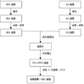
Fig. 4 is the flow chart of parallel transfer bonding process implementing.
Embodiment
In conjunction with Fig. 1, Fig. 2 and Fig. 3, the present invention is applied to the parallel transfer bonding techniques of germanium-silicon film that non-refrigerating infrared focal plane is manufactured, and taking mr-i9100m glue and ULTRA-i300 glue as example, sketches parallel transfer process respectively.
Wherein use the processing step of mr-i9100m glue as follows:
Step 1: as shown in the cleaning step in Fig. 3, according to RCA1 step, (ratio in 1 to 5 is mixed 25% NH3 solution and deionized water, after boiling, add H2O2 in 1 to 6 ratio, then by wafer submergence 10 minutes in solution) clean SOI wafer 2 and CMOS wafer 3, and dry up with nitrogen, be then placed in baking oven, at 200 DEG C, toast 30 minutes; Wherein SOI wafer 2 comprises silicon supporting layer 12, BOX layer 13, germanium-silicon film 14 successively, and CMOS wafer comprises metal electrode 17, cmos circuit 18, and metal electrode 17 is distributed in the back side of cmos circuit 18.
Step 2: as shown in the gluing step in Fig. 3, SOI wafer 2 and CMOS wafer 3 are placed on glue spreader, rotary coating mr-i9100m nano impression glue, forms SOI wafer bonding glue-line 15 and CMOS wafer bonding glue-line 16.(glue is thick to be determined by glue spreader rotating speed.Mr-i9100m glue, in the time that glue spreader rotating speed is 3000rpm, thick 1 μ of glue m)
Step 3: SOI wafer 2 and CMOS wafer 3 are placed on heating plate, and soft baking 2 minutes at 100 DEG C, to remove solvent.
Step 4: SOI wafer 2 and CMOS wafer 3 are placed in to baking oven, are heated to uniform temperature precuring bonding glue-line 15 and bonding glue-line 1630 minutes.(this step is optional.In general, the temperature of precuring and precuring, is to determine according to the type of glue and thickness, mr-i9100m glue, precuring 30 minutes at 160 DEG C)
Step 5: as shown in Figure 1, wafer, to being fixed on bonding fixture 1, is kept apart with pad 4 between wafer.As shown in Figure 2, then fixture is moved between the interior top board 8 in vacuumizing chamber 11 and lower platen 9 of bonder together with wafer, fixture is fixed on fixture fixing device 7, close vacuumizing chamber 11, be evacuated to 1.5*10-4Torr.
Step 6: as shown in Figure 1, 2, remove the pad 4 between wafer, by the pneumatic or hydraulic actuating mechanism 5 of bonder, wafer is applied the pressure of 3.5-4.0*105Pa.
Step 7: as shown in Figure 2, heat wafer by the heating plate 10 on upper lower platen, be warmed up to 200 DEG C with the speed of 7.5 DEG C/min, continue 50 minutes, lower the temperature by the chill plate 6 on upper lower platen afterwards, be cooled to 50 DEG C with the speed of 4 DEG C/min.
Step 8: as shown in Figure 2, actuator 5 stops applying bonding pressure, ventilates in vacuumizing chamber 11, opening operation chamber 11, takes out wafer pair, removes bonding fixture 1.Obtain the good wafer pair of bonding as shown in bonding step in Fig. 3.
Step 9: as shown in the attenuate step in Fig. 3, with N2 purge wafer pair, then by wafer to moving in the dark silicon etching machine of ICP, remove the silicon supporting layer 12 of SOI wafer.
Step 10: be 1 to 5 to being submerged into BHF(HF with the ratio of deionized water by the wafer of removing silicon supporting layer) (Immersion time is determined by BOX layer 13 thickness in solution, in typical case, BHF solution is 1000 A/min to the etch rate of SiO2), remove the BOX layer 13 on SOI wafer, take out wafer pair, so just completed quantum-well materials parallel transfer to CMOS wafer by SOI wafer.
Wherein use the processing step of ULTRA-i300 glue as follows:
Step 1: as shown in the cleaning step in Fig. 3, clean SOI wafer 2 and CMOS wafer 3 according to RCA1 step, and dry up with nitrogen, be then placed in baking oven, at 200 DEG C, toast 30 minutes.
Step 2: as shown in the gluing step in Fig. 3, SOI wafer 2 and CMOS wafer 3 are placed on glue spreader, rotary coating ULTRA-i300 glue, forms bonding glue-line 15 and bonding glue-line 16.(glue is thick to be determined by glue spreader rotating speed.ULTRA-i300 glue, in the time that glue spreader rotating speed is 3000rpm, thick 2 μ of glue m)
Step 3: SOI wafer 2 and CMOS wafer 3 are placed on heating plate, and soft baking 2 minutes at 70 DEG C, to remove solvent.
Step 4: as shown in Figure 1, wafer, to being fixed on bonding fixture 1, is kept apart with pad 4 between wafer.As shown in Figure 2, then fixture is moved between the interior top board 8 in vacuumizing chamber 11 and lower platen 9 of bonder together with wafer, fixture is fixed on fixture fixing device 7, close vacuumizing chamber 11, be evacuated to 1.5*10-4Torr.
Step 5: as shown in Figure 1, 2, remove the pad 4 between wafer, by the pneumatic or hydraulic actuating mechanism 5 of bonder, wafer is applied the pressure of 3.5-4.0*105Pa.
Step 6: as shown in Figure 2, heat wafer by the heating plate 10 on upper lower platen, be warmed up to 110 DEG C with the speed of 4 DEG C/min, continue 30 minutes, lower the temperature by the chill plate 6 on upper lower platen afterwards, be cooled to 50 DEG C with the speed of 3 DEG C/min.
Step 7: as shown in Figure 2, actuator 5 stops applying bonding pressure, ventilates in vacuumizing chamber 11, opening operation chamber 11, takes out wafer pair, removes bonding fixture 1.Obtain the good wafer pair of bonding as shown in bonding step in Fig. 3.
Step 8: as shown in the attenuate step in Fig. 3, with purging with nitrogen gas wafer pair, then by wafer to moving in the dark silicon etching machine of ICP, remove the silicon supporting layer 12 of SOI wafer.
Step 9: the wafer of removing silicon supporting layer, to being submerged in BHF solution, is removed to the BOX layer 13 on SOI wafer, take out wafer pair, so just completed quantum-well materials parallel transfer to CMOS wafer by SOI wafer.
Above technological process can have been explained parallel shifting process flow process of the present invention as example with the Type B thermosetting polymer bonding glue (mr-i9100m and ULTRA-i300) that oxygen plasma resist remover is removed using two kinds respectively.By series of process step, obtained as shown in Fig. 3 attenuate step taking bonding glue as sacrifice layer, there is the CMOS wafer of SiGe quantum wells material on top.