CN102208419B - Method for manufacturing semiconductor device and method for manufacturing display device - Google Patents
Method for manufacturing semiconductor device and method for manufacturing display device Download PDFInfo
- Publication number
- CN102208419B CN102208419B CN201110081650XA CN201110081650A CN102208419B CN 102208419 B CN102208419 B CN 102208419B CN 201110081650X A CN201110081650X A CN 201110081650XA CN 201110081650 A CN201110081650 A CN 201110081650A CN 102208419 B CN102208419 B CN 102208419B
- Authority
- CN
- China
- Prior art keywords
- conductive layer
- peristome
- layer
- insulating barrier
- film transistor
- Prior art date
- Legal status (The legal status is an assumption and is not a legal conclusion. Google has not performed a legal analysis and makes no representation as to the accuracy of the status listed.)
- Expired - Fee Related
Links
Images


Classifications
-
- H—ELECTRICITY
- H01—ELECTRIC ELEMENTS
- H01L—SEMICONDUCTOR DEVICES NOT COVERED BY CLASS H10
- H01L21/00—Processes or apparatus adapted for the manufacture or treatment of semiconductor or solid state devices or of parts thereof
- H01L21/02—Manufacture or treatment of semiconductor devices or of parts thereof
- H01L21/04—Manufacture or treatment of semiconductor devices or of parts thereof the devices having at least one potential-jump barrier or surface barrier, e.g. PN junction, depletion layer or carrier concentration layer
- H01L21/18—Manufacture or treatment of semiconductor devices or of parts thereof the devices having at least one potential-jump barrier or surface barrier, e.g. PN junction, depletion layer or carrier concentration layer the devices having semiconductor bodies comprising elements of Group IV of the Periodic System or AIIIBV compounds with or without impurities, e.g. doping materials
- H01L21/26—Bombardment with radiation
- H01L21/263—Bombardment with radiation with high-energy radiation
- H01L21/268—Bombardment with radiation with high-energy radiation using electromagnetic radiation, e.g. laser radiation
-
- H—ELECTRICITY
- H01—ELECTRIC ELEMENTS
- H01L—SEMICONDUCTOR DEVICES NOT COVERED BY CLASS H10
- H01L27/00—Devices consisting of a plurality of semiconductor or other solid-state components formed in or on a common substrate
- H01L27/02—Devices consisting of a plurality of semiconductor or other solid-state components formed in or on a common substrate including semiconductor components specially adapted for rectifying, oscillating, amplifying or switching and having at least one potential-jump barrier or surface barrier; including integrated passive circuit elements with at least one potential-jump barrier or surface barrier
- H01L27/12—Devices consisting of a plurality of semiconductor or other solid-state components formed in or on a common substrate including semiconductor components specially adapted for rectifying, oscillating, amplifying or switching and having at least one potential-jump barrier or surface barrier; including integrated passive circuit elements with at least one potential-jump barrier or surface barrier the substrate being other than a semiconductor body, e.g. an insulating body
- H01L27/1214—Devices consisting of a plurality of semiconductor or other solid-state components formed in or on a common substrate including semiconductor components specially adapted for rectifying, oscillating, amplifying or switching and having at least one potential-jump barrier or surface barrier; including integrated passive circuit elements with at least one potential-jump barrier or surface barrier the substrate being other than a semiconductor body, e.g. an insulating body comprising a plurality of TFTs formed on a non-semiconducting substrate, e.g. driving circuits for AMLCDs
- H01L27/124—Devices consisting of a plurality of semiconductor or other solid-state components formed in or on a common substrate including semiconductor components specially adapted for rectifying, oscillating, amplifying or switching and having at least one potential-jump barrier or surface barrier; including integrated passive circuit elements with at least one potential-jump barrier or surface barrier the substrate being other than a semiconductor body, e.g. an insulating body comprising a plurality of TFTs formed on a non-semiconducting substrate, e.g. driving circuits for AMLCDs with a particular composition, shape or layout of the wiring layers specially adapted to the circuit arrangement, e.g. scanning lines in LCD pixel circuits
-
- H—ELECTRICITY
- H01—ELECTRIC ELEMENTS
- H01L—SEMICONDUCTOR DEVICES NOT COVERED BY CLASS H10
- H01L27/00—Devices consisting of a plurality of semiconductor or other solid-state components formed in or on a common substrate
- H01L27/02—Devices consisting of a plurality of semiconductor or other solid-state components formed in or on a common substrate including semiconductor components specially adapted for rectifying, oscillating, amplifying or switching and having at least one potential-jump barrier or surface barrier; including integrated passive circuit elements with at least one potential-jump barrier or surface barrier
- H01L27/12—Devices consisting of a plurality of semiconductor or other solid-state components formed in or on a common substrate including semiconductor components specially adapted for rectifying, oscillating, amplifying or switching and having at least one potential-jump barrier or surface barrier; including integrated passive circuit elements with at least one potential-jump barrier or surface barrier the substrate being other than a semiconductor body, e.g. an insulating body
- H01L27/1214—Devices consisting of a plurality of semiconductor or other solid-state components formed in or on a common substrate including semiconductor components specially adapted for rectifying, oscillating, amplifying or switching and having at least one potential-jump barrier or surface barrier; including integrated passive circuit elements with at least one potential-jump barrier or surface barrier the substrate being other than a semiconductor body, e.g. an insulating body comprising a plurality of TFTs formed on a non-semiconducting substrate, e.g. driving circuits for AMLCDs
- H01L27/1248—Devices consisting of a plurality of semiconductor or other solid-state components formed in or on a common substrate including semiconductor components specially adapted for rectifying, oscillating, amplifying or switching and having at least one potential-jump barrier or surface barrier; including integrated passive circuit elements with at least one potential-jump barrier or surface barrier the substrate being other than a semiconductor body, e.g. an insulating body comprising a plurality of TFTs formed on a non-semiconducting substrate, e.g. driving circuits for AMLCDs with a particular composition or shape of the interlayer dielectric specially adapted to the circuit arrangement
-
- H—ELECTRICITY
- H01—ELECTRIC ELEMENTS
- H01L—SEMICONDUCTOR DEVICES NOT COVERED BY CLASS H10
- H01L27/00—Devices consisting of a plurality of semiconductor or other solid-state components formed in or on a common substrate
- H01L27/02—Devices consisting of a plurality of semiconductor or other solid-state components formed in or on a common substrate including semiconductor components specially adapted for rectifying, oscillating, amplifying or switching and having at least one potential-jump barrier or surface barrier; including integrated passive circuit elements with at least one potential-jump barrier or surface barrier
- H01L27/12—Devices consisting of a plurality of semiconductor or other solid-state components formed in or on a common substrate including semiconductor components specially adapted for rectifying, oscillating, amplifying or switching and having at least one potential-jump barrier or surface barrier; including integrated passive circuit elements with at least one potential-jump barrier or surface barrier the substrate being other than a semiconductor body, e.g. an insulating body
- H01L27/1214—Devices consisting of a plurality of semiconductor or other solid-state components formed in or on a common substrate including semiconductor components specially adapted for rectifying, oscillating, amplifying or switching and having at least one potential-jump barrier or surface barrier; including integrated passive circuit elements with at least one potential-jump barrier or surface barrier the substrate being other than a semiconductor body, e.g. an insulating body comprising a plurality of TFTs formed on a non-semiconducting substrate, e.g. driving circuits for AMLCDs
- H01L27/1259—Multistep manufacturing methods
- H01L27/127—Multistep manufacturing methods with a particular formation, treatment or patterning of the active layer specially adapted to the circuit arrangement
- H01L27/1274—Multistep manufacturing methods with a particular formation, treatment or patterning of the active layer specially adapted to the circuit arrangement using crystallisation of amorphous semiconductor or recrystallisation of crystalline semiconductor
- H01L27/1285—Multistep manufacturing methods with a particular formation, treatment or patterning of the active layer specially adapted to the circuit arrangement using crystallisation of amorphous semiconductor or recrystallisation of crystalline semiconductor using control of the annealing or irradiation parameters, e.g. using different scanning direction or intensity for different transistors
-
- H—ELECTRICITY
- H01—ELECTRIC ELEMENTS
- H01L—SEMICONDUCTOR DEVICES NOT COVERED BY CLASS H10
- H01L27/00—Devices consisting of a plurality of semiconductor or other solid-state components formed in or on a common substrate
- H01L27/02—Devices consisting of a plurality of semiconductor or other solid-state components formed in or on a common substrate including semiconductor components specially adapted for rectifying, oscillating, amplifying or switching and having at least one potential-jump barrier or surface barrier; including integrated passive circuit elements with at least one potential-jump barrier or surface barrier
- H01L27/12—Devices consisting of a plurality of semiconductor or other solid-state components formed in or on a common substrate including semiconductor components specially adapted for rectifying, oscillating, amplifying or switching and having at least one potential-jump barrier or surface barrier; including integrated passive circuit elements with at least one potential-jump barrier or surface barrier the substrate being other than a semiconductor body, e.g. an insulating body
- H01L27/1214—Devices consisting of a plurality of semiconductor or other solid-state components formed in or on a common substrate including semiconductor components specially adapted for rectifying, oscillating, amplifying or switching and having at least one potential-jump barrier or surface barrier; including integrated passive circuit elements with at least one potential-jump barrier or surface barrier the substrate being other than a semiconductor body, e.g. an insulating body comprising a plurality of TFTs formed on a non-semiconducting substrate, e.g. driving circuits for AMLCDs
- H01L27/1259—Multistep manufacturing methods
- H01L27/1292—Multistep manufacturing methods using liquid deposition, e.g. printing
-
- G—PHYSICS
- G02—OPTICS
- G02F—OPTICAL DEVICES OR ARRANGEMENTS FOR THE CONTROL OF LIGHT BY MODIFICATION OF THE OPTICAL PROPERTIES OF THE MEDIA OF THE ELEMENTS INVOLVED THEREIN; NON-LINEAR OPTICS; FREQUENCY-CHANGING OF LIGHT; OPTICAL LOGIC ELEMENTS; OPTICAL ANALOGUE/DIGITAL CONVERTERS
- G02F1/00—Devices or arrangements for the control of the intensity, colour, phase, polarisation or direction of light arriving from an independent light source, e.g. switching, gating or modulating; Non-linear optics
- G02F1/01—Devices or arrangements for the control of the intensity, colour, phase, polarisation or direction of light arriving from an independent light source, e.g. switching, gating or modulating; Non-linear optics for the control of the intensity, phase, polarisation or colour
- G02F1/13—Devices or arrangements for the control of the intensity, colour, phase, polarisation or direction of light arriving from an independent light source, e.g. switching, gating or modulating; Non-linear optics for the control of the intensity, phase, polarisation or colour based on liquid crystals, e.g. single liquid crystal display cells
- G02F1/133—Constructional arrangements; Operation of liquid crystal cells; Circuit arrangements
- G02F1/136—Liquid crystal cells structurally associated with a semi-conducting layer or substrate, e.g. cells forming part of an integrated circuit
- G02F1/1362—Active matrix addressed cells
-
- Y—GENERAL TAGGING OF NEW TECHNOLOGICAL DEVELOPMENTS; GENERAL TAGGING OF CROSS-SECTIONAL TECHNOLOGIES SPANNING OVER SEVERAL SECTIONS OF THE IPC; TECHNICAL SUBJECTS COVERED BY FORMER USPC CROSS-REFERENCE ART COLLECTIONS [XRACs] AND DIGESTS
- Y02—TECHNOLOGIES OR APPLICATIONS FOR MITIGATION OR ADAPTATION AGAINST CLIMATE CHANGE
- Y02P—CLIMATE CHANGE MITIGATION TECHNOLOGIES IN THE PRODUCTION OR PROCESSING OF GOODS
- Y02P80/00—Climate change mitigation technologies for sector-wide applications
- Y02P80/30—Reducing waste in manufacturing processes; Calculations of released waste quantities
Abstract
A method for manufacturing a semiconductor device and a method for manufacturing a display device. An object is to provide a method for manufacturing a highly-reliable semiconductor device with an improved material use efficiency and with a simplified manufacturing process. The method includes the steps of forming a conductive layer over a substrate, forming a light-transmitting layer over the conductive layer, and selectively removing the conductive layer and the light-transmitting layer by irradiation with a femtosecond laser beam from above the light-transmitting layer. Note that the conductive layer and the light-transmitting layer may be removed so that an end portion of the light-transmitting layer is located on an inner side than an end portion of the conductive layer. Before the irradiation with a femtosecond laser beam, a surface of the light-transmitting layer may be subjected to liquid-repellent treatment.
Description
The application is that application number is 200710142266X, and the applying date is on August 31st, 2007, and name is called the dividing an application of application for a patent for invention of " manufacture method of semiconductor device and the manufacture method of display device ".
Technical field
The present invention relates to utilize the manufacture method of the semiconductor element of the contact hole opening that uses femtosecond laser.In addition, the invention still further relates to the manufacture method of the semiconductor device with semiconductor element.
Background technology
The various films of stacked semiconductor film, dielectric film and conductive layer etc. on substrate suitably form the circuit that predetermined contact hole is made thin-film transistor (below be also referred to as " TFT ") and used this thin-film transistor by photoetching technique.Photoetching technique refers to utilize light will utilize on the transparent plate surface that is called as photomask the technology of pattern transfer on target substrate of circuit that non-light transmissive material forms etc.This photoetching technique is used in the manufacturing process of semiconductor integrated circuit etc. widely.And, so that the pattern that is transferred on the substrate with photoetching technique is mask, and by carrying out etching and remove becoming the dielectric film that exists in the part of contact hole, semiconductor film, metal film etc. at this, can form contact hole in desirable position.
In adopting the manufacturing process of existing photoetching technique, even if only use the processing of the mask pattern that the sensitization organic resin material that is called as photoresist forms, the multistage operation such as also need exposure, development, roasting, peel off.Therefore, the number of times of photo-mask process more increases, and manufacturing cost must more raise.In order to improve these problems, attempt to reduce photo-mask process and make TFT (for example, with reference to patent documentation 1).In patent documentation 1, use the Etching mask that forms by photo-mask process once after, again utilize as difform Etching mask after by expansion its volume being increased.
[patent documentation 1]
TOHKEMY 2000-133636 communique
Summary of the invention
Yet, when using this photo-mask process, owing to need to carry out at least five operations, i.e. emulsion coating, composition, development treatment, etch processes and lift-off processing, therefore until the operation end needs the expensive time, thereby productivity reduces.In addition and since use various medicines such as emulsion resist, be used for the developer that develops and the stripper that is used for peeling off etc., therefore in operation, can produce harmful waste liquid, the disposal cost of waste liquid also can increase manufacturing expense except the original cost of medicine.And, the environmental pollution that this medicine causes might occur.
In addition, be formed on the shape defect that adopts the conductive layer in the contact hole that this photo-mask process forms and cause bad connection between the conductive layer that connects by contact hole, become the rate of finished products of the semiconductor device that reduction can obtain and the reason of reliability.Particularly, when being formed for forming the wiring layer of circuit, the bad connection of wiring layer has caused bad impact to electrical characteristics, such as short circuit etc.
Problem of the present invention is for providing a kind of technology, wherein, make TFT and use the semiconductor device of TFT and the operation of the display device that formed by TFT in, reduction photo-mask process, and operation is simplified is with raising production capacity.In addition, the present invention also aims to provide with the controlled method that forms well the works of the wiring that consists of these display devices etc. of desirable shape.
The invention is characterized in, by coming in insulating barrier and conductive layer, to form peristome (contact hole) with femtosecond laser, and form the conductive layer that covers this peristome in this peristome by aqueous electric conducting material is ejected into.
The manufacture method of semiconductor device of the present invention is characterised in that, forms conductive layer at substrate, forms photic zone at described conductive layer, and optionally removes described conductive layer and described photic zone from described photic zone irradiation femtosecond laser.
The manufacture method of semiconductor device of the present invention is characterised in that, form conductive layer at substrate, form photic zone at described conductive layer, also optionally remove described conductive layer and described photic zone from described photic zone irradiation femtosecond laser and described conductive layer and described photic zone, form peristome, and aqueous electric conducting material is dropped onto in the described peristome.
In the manufacture method of semiconductor device of the present invention, also can be described euphotic end be configured to remove described conductive layer and described photic zone than the end mode more in the inner part of described conductive layer.
The manufacture method of semiconductor device of the present invention is characterised in that, form the first conductive layer at substrate, form photic zone at described the first conductive layer, from described photic zone irradiation femtosecond laser and optionally remove described the first conductive layer and described photic zone forms peristome described the first conductive layer and described photic zone, and aqueous electric conducting material dropped onto form the second conductive layer that is electrically connected with described the first conductive layer in the described peristome.
In the manufacture method of semiconductor device of the present invention, also can be described euphotic end be configured to remove described the first conductive layer and described photic zone than the end mode more in the inner part of described the first conductive layer.
In the manufacture method of semiconductor device of the present invention, also can hate liquid to process to described euphotic surface.
The present invention can also use in the display device as the device with Presentation Function.Be clipped in liquid crystal cell that light-emitting display device that the light-emitting component between the electrode is connected with TFT and use have liquid crystal material as the liquid crystal display device of display element etc. as the layer that uses display device of the present invention to have, will contain the mixture that manifests luminous organic substance, inorganic matter or organic substance and inorganic matter that is called as electroluminescence (below be also referred to as " EL ").
In said structure, can consist of the conductive layer that forms opening with in chromium, molybdenum, nickel, titanium, cobalt, copper or the aluminium one or more.In addition, can use the material through femtosecond laser, the organic resin etc. that has light transmission such as use consists of the photic zone that forms opening.
By the present invention, owing to can reduce complicated photo-mask process and make semiconductor device with the operation of having simplified, so the waste of material less and can realize the reduction of cost.Thereby can make to high finished product rate the display device of high-performance, high reliability.
Description of drawings
Fig. 1 is the sectional view of the manufacture method of explanation semiconductor device of the present invention.
Fig. 2 is the figure of the manufacture method of explanation semiconductor device of the present invention.
Fig. 3 is the sectional view of the manufacture method of explanation semiconductor device of the present invention.
Fig. 4 is the sectional view of the manufacture method of explanation semiconductor device of the present invention.
Fig. 5 is the figure of the manufacture method of explanation semiconductor device of the present invention.
Fig. 6 is the sectional view of the manufacture method of explanation semiconductor device of the present invention.
Fig. 7 is the figure of the manufacture method of explanation semiconductor device of the present invention.
Fig. 8 is the sectional view of the manufacture method of explanation semiconductor device of the present invention.
Fig. 9 is the figure that explanation can be applicable to the cross section structure of light-emitting component of the present invention.
Figure 10 is the sectional view of the manufacture method of explanation semiconductor device of the present invention.
Figure 11 is the figure that explanation can be applicable to the equivalent electric circuit of light-emitting component of the present invention.
Figure 12 is the sectional view of the manufacture method of explanation semiconductor device of the present invention.
Figure 13 is the figure that explanation can be applicable to the cross section structure of electrophoresis element of the present invention.
Figure 14 is the figure of the circuit structure of explanation when forming the scan line side drive circuit with TFT in display floater of the present invention.
Figure 15 is the figure (shift register circuit) of the circuit structure of explanation when forming the scan line side drive circuit with TFT in display floater of the present invention.
Figure 16 is the figure (buffer circuit) of the circuit structure of explanation when forming the scan line side drive circuit with TFT in display floater of the present invention.
Figure 17 is the vertical view of explanation semiconductor device of the present invention.
Figure 18 is the vertical view of explanation semiconductor device of the present invention.
Figure 19 is the stereogram that the electronic equipment of semiconductor device of the present invention is used in explanation.
Figure 20 is the figure that the electronic equipment of semiconductor device of the present invention is used in explanation.
Symbol description
720 substrates
721 conductive layers
722 photic zones
724 electric conducting materials
725 peristomes
726 conductive layers
Embodiment
Explain with reference to the accompanying drawings embodiments of the present invention.But the present invention is not limited to following explanation, and the fact that the ordinary person in affiliated field understands at an easy rate is exactly in the situation that does not break away from aim of the present invention and scope thereof, and its mode and detailed content can be transformed to various forms.Therefore, the present invention should not be interpreted as only being limited in the content that the execution mode that illustrates below puts down in writing.Note, in the structure of the present invention of explanation, in different accompanying drawings, represent identical part or have the part of said function with common Reference numeral, and omit its repeat specification below.
(execution mode 1)
In the present embodiment a kind of method will be described, it forms the conductive layer that covers this peristome by using femtosecond laser to form peristome (contact hole) and aqueous electric conducting material being ejected in this peristome.
At first, form conductive layer 721 (with reference to Figure 1A) at substrate 720.Note, as conductive layer 721, for example can use by containing and be selected from titanium (Ti), aluminium (Al), tantalum (Ta), tungsten (W), molybdenum (Mo), copper (Cu), chromium (Cr), neodymium (Nd), iron (Fe), nickel (Ni), cobalt (Co), ruthenium (Ru), rhodium (Rh), palladium (Pd), osmium (Os), iridium (Ir), silver (Ag), gold (Au), platinum (Pt), cadmium (Cd), zinc (Zn), silicon (Si), germanium (Ge), zirconium (Zr), individual layer or the lamination of the layer that the material of the element in the barium (Ba) consists of form.
Then, form photic zone 722 (with reference to Fig. 1 (A)) at conductive layer 721.At this, photic zone 722 so long as the film that is formed by the material that sees through laser just have no particular limits.For example, can form with organic resin of light transmission etc.In addition, also can hate liquid to process to the surface of photic zone 722.
Then, shine femtosecond laser (with reference to Fig. 1 (B)) from photic zone 722.Can by the surface irradiation femtosecond laser to photic zone 722, optionally remove conductive layer 721 and photic zone 722 (with reference to Fig. 1 (C)).In other words, on conductive layer 721 and photic zone 722, can optionally form peristome 725.At this, with the focal adjustments of femtosecond laser for being arranged in photic zone 722 or conductive layer 721.Note, in the fluctuating according to substrate, in the situation that the position of focus changes, also can give automatic focusing function to optical system.Note, even be arranged in the situation that photic zone 722 shines femtosecond laser in the focus with femtosecond laser, because this photic zone 722 is films, therefore be difficult to only optionally remove this photic zone 722.Therefore, the conductive layer 721 of lower floor also is removed together to be formed on and forms the peristome 725 that opening forms in conductive layer 721 and the photic zone 722.In addition, form in the situation of peristome shining like this femtosecond laser, also can be in peristome 725, the end mode more in the inner part that is formed on than conductive layer 721 according to the end of photic zone 722 forms.By adopting above-mentioned shape, can when peristome is keeping little bore, increase the area that exposes of conductive layer 721.Like this, can and use femtosecond laser to form opening by stacked conductive layer 721 and photic zone 722, form the little peristome of bore.Even this peristome by forming contact with the electroconductive resin material, also can form good syndeton.
Notice that femtosecond laser refers to that pulse duration is femtosecond (10
-15Second) the interior laser of scope.This femtosecond laser is launched from following laser oscillator.Can be as the laser as this laser oscillator, the alloy that can enumerate Nd, Yb, Cr, Ti, Ho, Er etc. adds Sapphire, YAG, ceramic YAG, ceramic Y to
2O
3, KGW, KYW, Mg
2SiO
4, YLF, YVO
4, GdVO
4Deng crystallization in laser etc.
In the present embodiment, owing to can form peristome 725 by using laser selective ground, therefore do not need to form mask layer, can reduce operation and material.In addition, because can be by focusing on the very little luminous point with femtosecond laser, so conductive layer and the insulating barrier of this processing can be processed into predetermined shape accurately.And, owing to be to heat to moment at short notice, thereby have almost the advantage that need not heat the zone outside the machining area.In addition, by using femtosecond laser, can easily process the material that sees through light (hardly absorption optical).In addition, can adopt single operation to process the film that different material layers is stacked as multilayer.
Then, aqueous electric conducting material 724 is dropped onto (with reference to Fig. 1 (D)) in the peristome 725.At this, adopt drop ejection (injections) method (being also referred to as ink-jet method according to its mode), this drop sprays drop that method can optionally spray the composition that (injection) prepare for specific purpose conductive layer etc. is formed predetermined pattern.The aqueous electric conducting material (drop) 724 that will comprise works formation material is ejected in the peristome 725, carries out the fixing such as roasting, drying, has the conductive layer 726 (with reference to Fig. 1 (E)) of desirable pattern with formation.
At this, will be shown in Fig. 2 for a mode of the droplet ejection apparatus of drop ejection method.Each shower nozzle 1405,1412 of droplet ejection apparatus 1403 is connected to control device 1407, can draw into the in advance pattern of design by computer 1410 to its control device that carries out.As the opportunity of drawing, for example can carry out as standard take the mark 1411 that is formed on the substrate 1400.Perhaps, also can be take the edge of substrate 1400 determine reference point as standard.By camera head 1404
Measure this reference point, in image processing apparatus 1409, be converted to digital signal, identify to produce control signal by computer 1410, and be sent in the control device 1407.As camera head 1404, can use imageing sensor that utilizes charge coupled cell (CCD) and complementary metal oxide semiconductors (CMOS) etc.Certainly, the information that is formed on the pattern on the substrate 1400 is stored in the storage medium 1408, to control device 1407 transfer control signals, and can control respectively each shower nozzle 1405,1412 of droplet ejection apparatus 1403 according to this information.The material of ejection is supplied to respectively the shower nozzle 1405,1412 by conduit from material supply source 1413, material supply source 1414.
The inside of shower nozzle 1405 is to have the space of filling like that liquid material shown in dotted line 1406 and as the structure of the nozzle of ejiction opening.Although not shown, shower nozzle 1412 also has the internal structure identical with shower nozzle 1405.When with mutually different size the nozzle of shower nozzle 1405 and shower nozzle 1412 being set, can draw simultaneously different materials with different width.Can only spray respectively electric conducting material and organic and inorganic material etc. with a shower nozzle and draw, and in the situation of in the extensive region such as interlayer film, drawing, in order to boost productivity, can to spray simultaneously identical material by a plurality of nozzles and draw.In the situation of using large-sized substrate, can to the scanning direction shown in the arrow freely, freely set the zone of drawing, and can draw a plurality of identical patterns at a substrate at substrate upper nozzle 1405,1412.
Adopting drop ejection method to form in the situation of conductive layer, contain the composition that is processed as emboliform electric conducting material by ejection, and by burning till its fusion or welding are solidified, thereby form conductive layer.Although the major part of the conductive layer (perhaps insulating barrier) that employing sputtering method etc. forms shows column structure, is containing the composition of electric conducting material by ejection and is burning till the polycrystalline state that the main demonstration of the conductive layer (perhaps insulating barrier) that forms has a plurality of crystal boundaries like that as mentioned above.
In the present embodiment, by coming with femtosecond laser in photic zone 722, to form peristome 725, and by adopting drop ejection method to come in this peristome 725, to form conductive layer 726.Accordingly, can form peristome, and not carry out complicated photo-mask process, and this conductive layer 726 can with photic zone 722 under conductive layer 721 electrically contact well, and be not subject to the impact of the shape of this peristome.For example, in peristome 725, even if be formed on than the end of conductive layer 721 more in the inner part in the narrow situation of the situation of (peristome is back taper) or peristome in the end of photic zone 722, because conductive layer 726 forms by aqueous electric conducting material is ejected in the peristome, thereby can electrically contact well with conductive layer 721.
In addition, in the present embodiment, also can before photic zone 722 is shone femtosecond lasers, hate liquid to process to the surface of photic zone 722.Process by the surface of photic zone 722 being hated liquid, can prevent following situation: when in peristome 725, forming conductive layer 726, aqueous electric conducting material (drop) 724 is layered on the surface of photic zone 722, and do not enter into peristome 725, can precision better electric conducting material 724 be flow in the peristome 725.
(execution mode 2)
In the present embodiment, the manufacture method for the semiconductor device of the method that adopts execution mode 1 illustrates with reference to Fig. 3 A to 3F.
At this, as semiconductor device, use the staggered thin-film transistor of counter-rotating (staggered TFT reverses) to illustrate.Note, also can make the semiconductor element of quadrature shift thin-film transistor, coplanar type thin-film transistor, diode, MOS transistor etc., and be not limited to the staggered thin-film transistor of counter-rotating.
At first, form gate electrode layer 182 (with reference to Fig. 3 (A)) at substrate 100.Substrate 100 can use glass substrate, quartz substrate, the metal substrate that is made of barium borosilicate glass, aluminium borosilicate glass etc. or the stable on heating plastic with the treatment temperature that can bear this manufacturing process.In addition, also can polish by CMP method etc., so that the surfacing of substrate 100.Note, also can form insulating barrier at substrate 100.Insulating barrier uses the oxide material, the nitride material that contain silicon by the whole bag of tricks of CVD method, plasma CVD method, sputtering method, whirl coating etc., and forms with individual layer or lamination.Also can not form this insulating barrier, but have blocking from the effect of the polluter of substrate 100 etc.
Adopt form conductive layer such as sputtering method, PVD (physical vapor deposition) method, such as CVD (chemical vapor deposition) method etc. of decompression CVD method (LPCVD method) or plasma CVD method etc. after, by photo-mask process conductive layer is optionally carried out etching, can form gate electrode layer 182.In addition, as the electric conducting material that forms gate electrode layer 182, can use the element that is selected among Ag, Au, Ni, Pt, Pd, Ir, Rh, Ta, W, Ti, Mo, Al, the Cu or with alloy material or the compound-material of described element as main component.In addition, also can use with the polysilicon film of the impurity elements such as Doping Phosphorus semiconductor film, the AgPdCu alloy as representative.In addition, it can be the structure of single layer structure or a plurality of layers, for example, both can be the double-decker of tungsten nitride film and molybdenum (Mo) film, can be again that stacked film thickness is that the tungsten film of 50nm, aluminium that film thickness is 500nm and alloy film, the film thickness of silicon are the three-decker of the titanium nitride film of 30nm in order.In addition, in the situation that adopts three-decker, both can use tungsten nitride to replace the tungsten of the first conducting film, and can use again the alloy film of aluminium and titanium to replace the aluminium of the second conducting film and the alloy film of silicon.And, can also use titanium film to replace the titanium nitride film of the 3rd conducting film.
In the present embodiment, optionally spray composition and form gate electrode layer.When like this optionally forming gate electrode layer, has the effect of simplifying manufacturing procedure.
Then, form gate insulation layer 180 (with reference to Fig. 3 (A)) at substrate 100 and gate electrode layer 182.As gate insulation layer 180, form with the material of the oxide material of silicon or nitride material etc. and to get final product, and can be lamination or individual layer.In the present embodiment, use the lamination of the bilayer of silicon nitride film, silicon oxide film.In addition, also can adopt the individual layer of this lamination, oxygen silicon nitride membrane or by the lamination that consists of more than three layers.The preferred silicon nitride film with fine and close film character that uses.In addition, silver and copper being used in the situation that adopts the conductive layer that drop ejection method forms, when forming the plain film of stopping up and NiB film as barrier film thereon, have the diffusion that prevents impurity and the fruit that makes surfacing.Notice that in order to form grid leakage current less under lower film-forming temperature and fine and close dielectric film, preferably the rare gas element with argon etc. is included in the reacting gas, and is blended in the dielectric film that will form.At this, by plasma CVD method, form the silicon nitride layer of 50~200nm.
Then, the gate insulation layer 180 at substrate 100 forms semiconductor layer 185a.As the material that forms semiconductor layer 185a, can use the semiconductor material gas take silane and germane as representative and adopt chemical vapour deposition and amorphous semiconductor that sputtering method is made (below be also referred to as " AS "), utilize luminous energy and heat energy to make the poly semiconductor of this amorphous semiconductor crystallization or hemihedral crystal (being also referred to as crystallite or " SAS ") semiconductor etc.Note, can adopt drop ejection method to form semiconductor layer 185a, this drop ejection method forms the layer with reservation shape from the drop of the composition that fine hole ejection process is adjusted.In addition, also can adopt print process to form.In addition, also can adopting CVD method, PVD method, coating process etc. after substrate forms semiconductor layer, optionally conductive layer be carried out etching by photo-mask process and form semiconductor layer 185a.
As amorphous semiconductor, can typically enumerate amorphous silicon hydride, and as crystal semiconductor, can typically enumerate polysilicon etc.Polysilicon comprise use the polysilicon that forms with the processing temperature more than 800 ℃ as the so-called high temperature polysilicon of main material, use the polysilicon that forms with the processing temperature below 600 ℃ as the so-called low temperature polycrystalline silicon of main material and add the polysilicon etc. that the element that promotes crystallization etc. comes crystallization.Certainly, also can use the semiconductor that in the part of hemihedral crystal semiconductor or semiconductor layer, contains crystalline phase.
Notice that SAS is a kind of semiconductor, it has the intermediate structure between non crystalline structure and the crystalline texture (comprising monocrystalline and polycrystalline), and has the third state stable aspect free energy, also comprises the crystal region with shortrange order and distortion of lattice.Can observe the crystal region of 0.5~20nm in film at least a portion zone, when take silicon as main component, Raman spectrum is transferred to and is compared 520cm
-1Low wave number one side.In X-ray diffraction, observe (111), the diffraction peak of (220) that the lattice by silicon causes.Contain at least 1 atom % or the more hydrogen or halogen that is used for termination suspension key (dangling bonds).Form SAS by siliceous gas being carried out glow discharge decomposition (plasma CVD).As siliceous gas, can use SiH
4, in addition can also use Si
2H
6, SiH
2Cl
2, SiHCl
3, SiCl
4, SiF
4Deng.In addition, also can mix F
2, GeF
4Can also use H
2, or H
2With one or more rare gas that are selected from He, Ar, Kr and Ne this siliceous gas is diluted.Dilution ratio is that pressure is roughly in the scope of 0.1Pa~133Pa in 2~1000 times the scope, and supply frequency is 1MHz~120MHz, is preferably 13MHz~60MHz.Substrate heating temperature is preferably below 300 ℃, and also can form with 100~200 ℃ substrate heating temperature.At this, as the impurity element that mainly mixes when the film forming, preferably the impurity such as oxygen, nitrogen or carbon etc. from Atmospheric components is 1 * 10
20Cm
-3Below, especially oxygen concentration is 5 * 10
19Cm
-3Below, be preferably 1 * 10
19Cm
-3Below.In addition, by adding such as helium, argon, krypton or neon etc. of rare gas element, improve stability with further reinforcement distortion of lattice, thereby can obtain good SAS.In addition, as semiconductor layer, SAS layer that can also lamination is formed by hydrogen class gas on the SAS layer that is formed by fluorine type gas.
When using crystalline semiconductor layer in semiconductor layer, the manufacture method of this crystalline semiconductor layer can adopt the whole bag of tricks (the thermal crystallization method of the element of the promotion crystallization of laser crystallization, thermal crystallization method or use nickel etc. etc.).In addition, also can come crystallization to the micro-crystallization semiconductor irradiating laser as SAS, to improve crystallinity.In the situation of not introducing the element that promotes crystallization, before to the amorphous silicon film irradiating laser, by under blanket of nitrogen, 500 ℃ of lower heating one hour, make the hydrogen concentration that contains of amorphous silicon film be released into 1 * 10
20Atom/cm
3Below.This is because when when containing the amorphous silicon film irradiating laser of a large amount of hydrogen, the cause that amorphous silicon film is destroyed.
As the method for noncrystal semiconductor layer being introduced metallic element, so long as can make this metallic element be present on the surface of noncrystal semiconductor layer or its inner method, then have no particular limits, for example can use the method for the solution of sputtering method, CVD method, plasma processing method (comprising plasma CVD method), absorption method, plating salt.In said method, use the method for solution simple, be easy to adjust aspect the concentration of metallic element useful.In addition, preferably contain the Ozone Water of hydroxyl or the processing of hydrogen peroxide etc. and form oxide-film by irradiation UV light, thermal oxidation method, use in oxygen atmosphere this moment, in order to improve the wettability on the surface of noncrystal semiconductor layer, and the aqueous solution is diffused in the whole surface of noncrystal semiconductor layer.
Both can make up the crystallization of carrying out noncrystal semiconductor layer by the crystallization of heat treatment and Ear Mucosa Treated by He Ne Laser Irradiation, can repeatedly heat-treat individually or Ear Mucosa Treated by He Ne Laser Irradiation again.In addition, also can pass through plasma method, crystalline semiconductor layer is formed directly on the substrate.
In addition, can form semiconductor with organic semiconducting materials and by print process, distributor method, gunite, whirl coating, drop ejection method etc.In the case, because do not need above-mentioned etching work procedure, can reduce process number.As organic semiconductor, can use low molecular material, macromolecular material etc., can also use the materials such as organic pigment, conductive polymer material.As being used in organic semiconducting materials of the present invention, preferably adopt the macromolecular material of the pi-electron conjugated system that its skeleton is made of conjugated double bond.Typically be, can use polythiophene, poly-fluorenes, poly-(3-alkylthrophene), polythiofuran derivative, pentacene etc.
Have as in addition being used in organic semiconducting materials of the present invention, by after the precursor film forming with solubility, processing, can form the material of semiconductor layer.Note as this organic semiconducting materials polythiophene ethene, poly-(2,5-thiofuran ethylene), polyacetylene, Polyacetylene Derivatives, poly-propine ethene etc. being arranged.
When precursor is converted to organic semiconductor, not only carry out heat treated, but also the catalysts of interpolation hydrogen chloride gas etc.In addition, typical solvent as making these soluble organic semiconductor material dissolvings can be suitable for toluene, dimethylbenzene, chlorobenzene, dichloro-benzenes, methyl phenyl ethers anisole, chloroform, carrene, gamma-butyrolacton, butyl cellosolve, cyclohexane, NMP (METHYLPYRROLIDONE), cyclohexanone, 2-butanone, two
 Alkane, dimethyl formamide (DMF) or THF (oxolane) etc.
Then, form the semiconductor layer 186 (with reference to Fig. 3 (B)) with a conductivity type at semiconductor layer 185a.Semiconductor layer 186 with a conductivity type plays a role as source area and drain region.Note, form as required the semiconductor film with a conductivity type and get final product, and can form the semiconductor film with N-shaped that comprises the impurity element (P, As) of giving N-shaped and the semiconductor film with p-type that comprises the impurity element (B) of giving p-type.In addition, can adopt drop ejection method to form the semiconductor layer 186 with a conductivity type, this drop ejection method has the layer of reservation shape through the drop formation of the composition of adjustment from fine hole ejection.Also can adopt print process to form.In addition, passing through CVD method, PVD method, coating process etc. after substrate forms, also can optionally carry out etching by photo-mask process, form the semiconductor layer 186 with a conductivity type.
Then, form wiring 187 (with reference to Fig. 3 (C)) at the semiconductor layer 186 with a conductivity type.As wiring 187 formation method, can and burn till by drop ejection method drippage conductive paste and form.In addition, also can adopt print process to form.In addition, also can optionally carry out etching by photo-mask process to this conductive layer passing through CVD method, PVD method, coating process etc. after substrate forms conductive layer, form wiring 187.
Wiring 187 plays a role as source electrode layer or drain electrode layer, and is electrically connected with the semiconductor layer 186 with a conductivity type.Electric conducting material as forming wiring 187 can use with the composition of the metallics such as Ag (silver), Au (gold), Cu (copper), W (tungsten), Al (aluminium) as main component.In addition, also can make up the tin indium oxide (ITO) with light transmission, the tin indium oxide (ITSO) that contains silica, organo indium, organotin, zinc oxide, titanium nitride etc.
In addition, form by using drop ejection method, form with whole coating by whirl coating etc. and compare the waste that can prevent material, can reduce cost.
Then, form insulating barrier 183 (with reference to Fig. 3 (D)) in wiring 187.As the material of insulating barrier 183, so long as the photic zone that is formed by the material that sees through laser then has no particular limits.For example, can use by the film of one or more formations in the organic material (organic resin material) (polyimides, propylene, polyamide, polyimides-acid amides, resist, benzocyclobutene etc.) of inorganic material (silica, silicon nitride, silicon oxynitride, silicon oxynitride etc.), sensitization or non-photosensitive, advanced low-k materials etc. or lamination of above-mentioned film etc.In addition, also can use silicone compositions.In addition, also can hate liquid to process to the surface of insulating barrier 183.
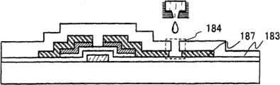
Then, in insulating barrier 183, form peristome 184 (with reference to Fig. 3 (E)).In the present embodiment, such as shown in Embodiment 1, by to desirable position irradiation femtosecond laser, can form peristome 184 on the desirable position in wiring 187 and insulating barrier 183.
Then, in peristome 184, the composition that ejection contains electric conducting material forms electrode layer 181 (with reference to Fig. 3 (E), 3 (F)).When optionally spraying composition and form electrode layer, has the effect that manufacturing procedure is simplified.
Note, also can adopt the porous body of polyvinyl alcohol to clean and polishing electrode layer 181 by the CMP method, in order to make its surfacing.In addition, also can after the polishing of adopting the CMP method, carry out ultraviolet ray irradiation, oxygen plasma treatment etc. to the surface of electrode layer 181.
By above-mentioned operation, finish the bottom gate thin film transistor 188 that is formed on the substrate 100 and are connected the semiconductor element that connects with electrode layer.
In the present embodiment, come in insulating barrier 183, to form peristome 184 with femtosecond laser, and in this peristome 184, form electrode layer 181 by drop ejection method.Because form peristome with femtosecond laser in the present embodiment, so came for forming peristome in conductive layer and the insulating barrier, can form peristome with single operation, and not adopt photo-mask process for need to carry out complicated photo-mask process in the past.And owing to form the electrode layer that covers peristome with drop ejection method, so this electrode layer 181 can electrically contact well with the wiring 187 under insulating barrier, and is not subject to the impact of the shape of this peristome.For example, in peristome 184, even if be formed on than wiring 187 end more in the inner part in the narrow situation of the situation of (peristome is back taper) or peristome in the end with insulating barrier 183, because electrode layer 181 forms by the aqueous electric conducting material of ejection in peristome, therefore also can electrically contact well with wiring 187.
In addition, in the present embodiment, also can before insulating barrier 183 is shone femtosecond lasers, hate liquid to process to the surface of insulating barrier 183.Process by the surface of insulating barrier 183 being hated liquid, can prevent following situation: when forming electrode layer 181 in the peristome 184, aqueous electric conducting material (drop) is laminated on the surface of insulating barrier 183, can electric conducting material be flow in the peristome 184 precision and do not enter in the peristome 184.
By adopting the manufacture method of the semiconductor device shown in the present embodiment, can form the opening (contact hole) between the wiring, and not adopt complicated photo-mask process, and obtain electrically contacting of good wiring.Therefore the waste of material is few, and can make to high finished product rate the semiconductor device of high function and high reliability.
Execution mode 3
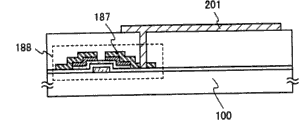
In the present embodiment, use Fig. 4 explanation to have the manufacture method of the semiconductor device of the conductive layer that is connected to thin-film transistor.At this, form display panels as semiconductor device.In addition, the sectional view of a pixel of display panels shown in Figure 4, and be described below.
Shown in Fig. 4 (A), form the thin-film transistor 188 shown in the execution mode 2 and the insulating barrier 190 of cover film transistor 188 at substrate 100.At this, by the coating process coating composition and burn till to form the insulating barrier 190 that is consisted of by polyimides.
Then, in the part of insulating barrier 190, the method according to shown in the execution mode 1 arranges peristome with femtosecond laser, has the insulating barrier 190 of peristome with formation.Also can after remove and be formed on wiring 187 lip-deep oxide.
Then, shown in Fig. 4 (B), form the conductive layer 192 that is connected to wiring 187 on the surface of peristome and insulating barrier 190.Notice that conductive layer 192 plays a role as pixel electrode, adopts drop ejection method optionally to form.By the conductive layer 192 that formation has light transmission, the back can form the transmission-type light emitting display panel.In addition, have reflexive conductive layer as conductive layer 192 by forming such as Ag (silver), Au (gold), Cu (copper), W (tungsten), Al (aluminium) etc., can make in the back the reflective light-emitting display floater.And, have the conductive layer of light transmission and have reflexive conductive layer by formation is above-mentioned in each pixel, can make the Semitransmissive display floater.
Notice that shown in Fig. 4 (B), peristome can be formed on the surface of wiring 187 according to wiring 187 and conductive layer 192 contacted modes.
In addition, shown in Fig. 4 (C), peristome can be formed on the surface of the semiconductor layer 186 with a conductivity type according to the semiconductor layer 186 with a conductivity type and conductive layer 192 contacted modes.
By above-mentioned operation, can form active array substrate.
Then, form dielectric film by print process or spin-coating method, carry out friction treatment and form alignment films 193 (with reference to Fig. 4 (D)).In addition, also can adopt the oblique evaporation method to form alignment films 193.
Then, in the relative substrate 261 that is provided with alignment films 264, the second pixel electrode (opposite electrode) 263 and dyed layer 262, in the peripheral region of pixel section, form the encapsulant (not shown) with closed loop shape by drop ejection method.Filler can be mixed in the encapsulant, and, also can form colored filters and Protective film (black matrix) etc. at relative substrate 261.
Then, liquid crystal material is dropped in the inboard of the closed loop that is formed by encapsulant by distributor mode (drippage mode), then, fit in a vacuum relative substrate and active array substrate, and carry out ultraviolet curing and form the liquid crystal layer 265 that is filled with liquid crystal material.Note, as the method that forms liquid crystal layer 265, also can use after the relative substrate of fitting to replace distributor mode (drippage mode) by the impregnation method (pouring into mode) that uses capillarity to inject liquid crystal material.
Then, with wiring board, be typically the splicing ear section that FPC (flexible print circuit) attaches to scan line and holding wire by connecting conductive layer.By above-mentioned operation, can form display panels.
Notice that although present embodiment illustrates the liquid crystal panel of TN type, said process also can similarly be applied to the liquid crystal panel of other modes.For example, present embodiment can be applied to apply abreast the liquid crystal panel that electric field makes the lateral electric field type of liquid crystal aligning with glass substrate.In addition, present embodiment can be applied to the liquid crystal panel of VA (vertical orientated) mode.
Fig. 5 and Fig. 6 illustrate the dot structure of VA type liquid crystal panel.Fig. 5 is plane graph, and Fig. 6 illustrates the cross section structure corresponding to cut-out line I-J shown in Figure 5.Describe with reference to these two figure in the description shown below.
In this dot structure, in a pixel, have a plurality of pixel electrodes, and TFT is connected to each pixel electrode.Each TFT is according to being driven by different signals and consisting of.In other words, has following structure, i.e. the independent signal that imposes on each pixel electrode of controlling in the pixel with many quadrant designs.
Same with execution mode 1, make pixel electrode layer 1624 and pixel electrode layer 1626 with the drop ejection operation with two operations.Specifically, comprise the composition of the first electric conducting material by the first drop ejection operation along the profile ejection of the pattern of pixel electrode layer, form the first conductive layer of frame shape.Mode with the first conductive layer inside of filling the frame shape sprays the composition that comprises the second electric conducting material, to form the second conductive layer.The first conductive layer and the second conductive layer can be used as continuous pixel electrode layer, and can form pixel electrode layer 1624,1626.Adopt like this present invention, because the waste of material is simplified and prevented to operation, thereby can make well display device with low cost and productivity.
Like this, can make liquid crystal panel as pixel electrode layer with the composite material that organifying compound and inorganic compound Composite form.By using pixel electrodes, do not need to use with the nesa coating of indium as principal component, thereby can remove bottleneck problem on aspect the raw material.
Present embodiment can suitably freely make up with above-mentioned execution mode.
Note, can be between splicing ear and source wiring (grid wiring) or in pixel section, be provided for preventing the protective circuit of electrostatic breakdown, it is typically diode etc.In this case, make by adopting the operation identical with above-mentioned TFT, and the grid wiring layer of pixel section is connected to drain electrode or the source wiring layer of diode, can prevent electrostatic breakdown.
By the manufacture method of the display panels shown in the present embodiment, can form the opening (contact hole) between the wiring, and not use complicated photo-mask process and good the electrically contacting that can obtain to connect up.Therefore the waste of material is few, and can make to high finished product rate the display panels of high function and high reliability.
(execution mode 4)
In the present embodiment, the method that has a semiconductor device of the conductive layer that is connected to thin-film transistor for manufacturing describes.At this, form pixel electrode as conductive layer, and form light emitting display panel as semiconductor device.A pixel of light emitting display panel shown in Figure 8, and be described below.
Shown in Fig. 8 (A), form thin-film transistor 188 and the cover film transistor 188 shown in the execution modes 2 and have the insulating barrier 191 of the peristome that uses the femtosecond laser opening at substrate 100.
Then, shown in Fig. 8 (B), similarly form the first conductive layer 201 that is connected to wiring 187 with execution mode 1 or execution mode 2.Notice that the first conductive layer 201 plays a role as pixel electrode.
Then, shown in Fig. 8 (C), form the insulating barrier 202 that covers the first conductive layer 201 ends that play a role as pixel electrode.This insulating barrier can be by forming not shown insulating barrier at insulating barrier 191 and the first conductive layer 201, and this insulating barrier irradiation femtosecond laser is removed the insulating barrier on the first conductive layer 201 and formed.
Then, form the layer 203 with luminescent substance at the exposed division of the first conductive layer 201 and the part of insulating barrier 202, and form the second conductive layer 204 that plays a role as pixel electrode thereon.By above-mentioned operation, can form by conductive layer 201, have the light-emitting component 205 that consists of of layer the 203 and second conductive layer 204 of luminescent substance.
At this, with the structure of explanation light-emitting component 205.
By form to use organic compound and have the layer (below, be called luminescent layer 343) of lighting function in containing the layer 203 of luminescent substance, light-emitting component 205 is as organic EL performance function.
As luminiferous organic compound, for example can enumerate (the abbreviation: DNA) of 9,10-two (2-naphthyl) anthracene; The 2-tert-butyl group-9, (the abbreviation: t-BuDNA) of 10-two (2-naphthyl) anthracene; 4,4 '-(abbreviation: DPVBi) of two (2,2-diphenylacetylene) biphenyl; Cumarin 30; Coumarin 6; Cumarin 545; Cumarin 545T; Perylene; Rubrene; Pyridine alcohol (periflanthene); (the abbreviation: TBP) of 2,5,8,11-four (tert-butyl group) perylene; (the abbreviation: DPA) of 9,10-diphenylanthrancene; 5,12-diphenyl aphthacene; 4-(dicyano methylene)-2-methyl-6-[p-(dimethylamine) styryl]-(abbreviation: DCM1) of 4H-pyrans; 4-(dicyano methylene)-2-methyl-6-[2-(julolidine-9-yl) vinyl]-(abbreviation: DCM2) of 4H-pyrans; 4-(dicyano methylene)-2, two [p-(dimethylamine) the styryl]-4H-pyrans (abbreviations: BisDCM) etc. of 6-.In addition, can launch the compound of phosphorescence below also can using: two [2-(4 ', 6 '-difluorophenyl) pyridine-N, C
2] (the abbreviation: FIrpic) of (picoline) iridium; Two 2-[3 ', 5 '-two (trifluoromethyl) phenyl] pyridine-N, C
2(the abbreviation: Ir (CF of (picoline) iridium
3Ppy)
2(pic)); Three (2-phenylpyridine-N, C
2) iridium (abbreviation: Ir (ppy)
3); (acetylacetone,2,4-pentanedione) two (2-phenylpyridine-N, C
2) iridium (abbreviation: Ir (ppy)
2(acac)); (acetylacetone,2,4-pentanedione) two [2-(2 '-thienyl) pyridine-N, C
3) iridium (abbreviation: Ir (thp)
2(acac)); (acetylacetone,2,4-pentanedione) two (2-phenylchinoline-N, C
2) iridium (abbreviation: Ir (pq)
2(acac)); (acetylacetone,2,4-pentanedione) two [2-(2 '-benzothiophene) pyridine-N, C
3) iridium (abbreviation: Ir (btp)
2(acac)) etc.
In addition, shown in Fig. 9 A, also can form light-emitting component 205 by the 1st conductive layer 201, layer 203 and second conductive layer 204 that contain luminescent material, the hole injection layer 341 that the described layer 203 that contains luminescent material is formed by hole-injecting material, the hole transmission layer 342 that is formed by hole mobile material, the luminescent layer 343 that is formed by luminiferous organic compound, the electron transfer layer 344 that is formed by electron transport material and formed by the electron injecting layer 345 that electron injection material forms.
As hole mobile material, can enumerate phthalocyanine (abbreviation: H
2Pc); CuPc (abbreviation: CuPc); Ranadylic phthalocyanine (abbreviation: VOPc); 4,4 ', 4 " three (N, N-diphenylamines) triphenylamine (abbreviations: TDATA); 4,4 ', 4 " three [N-(3-aminomethyl phenyl)-N-aniline] triphenylamine (abbreviations: MTDATA); (the abbreviation: m-MTDAB) of 1,3,5-three [N, N-two (meta-tolyl) amino] benzene; N, N '-diphenyl-N, N '-two (3-aminomethyl phenyl)-1,1 '-biphenyl-4,4 '-diamines (abbreviation: TPD); 4,4 '-(abbreviation: NPB) of two [N-(1-naphthyl)-N-aniline] biphenyl; 4,4 '-two (N-[4-two (meta-tolyl) amino] phenyl-N-aniline } biphenyl (abbreviation: DNTPD); 4,4 '-(abbreviation: BBPB) of two [N-(4-xenyl)-N-aniline] biphenyl; 4,4 ', 4 " three (N-carbazyl) triphenylamine (abbreviations: TCTA) etc., but be not limited to these materials.In addition, in above-mentioned compound, producing easily the hole take TDATA, MTDATA, m-MTDAB, TPD, NPB, DNTPD, BBPB, TCTA etc. as typical aromatic amine compound, is preferred compound group as organic compound therefore.Material described here is mainly to have 10
-6Cm
2The material of the hole mobility that/Vs is above.
Except above-mentioned hole mobile material, hole-injecting material also comprise chemical doping Electroconductivity of Conducting Polymers, also can use the poly styrene sulfonate that mixed (abbreviation: polyethylene dioxythiophene PSS) (abbreviation: PEDOT), polyaniline (abbreviation: PAni) etc.And the ultrathin membrane of the film of inorganic semiconductor such as molybdenum oxide, vanadium oxide, nickel oxide etc. or inorganic insulator such as aluminium oxide etc. is also effective.
Here, as electron transport material, can use the material that is consisted of by the metal complex with chinoline backbone or benzoquinoline skeleton etc., for example, (the abbreviation: Alq of three (oxine) aluminium
3), three (4-methyl-oxine) aluminium (abbreviation: Almq
3), two (10-hydroxy benzo [h]-quinoline) beryllium (abbreviation: BeBq
2), two (2-methyl-oxine)-4-phenyl phenates-aluminium (abbreviation: BAlq) etc.In addition, in addition, can also use to have
The material of the metal complex of azoles ligand or thiazole ligand etc., for example, two [2-(2-hydroxyphenyl) benzos
 Azoles] zinc (abbreviation: Zn (BOX)
2), two [2-(2-hydroxyphenyl) benzothiazole] zinc (abbreviation: Zn (BTZ)
2) etc.In addition, except metal complex, can also use 2-(4-xenyl)-5-(4-tert-butyl-phenyl)-1,3,4-
Azoles] zinc (abbreviation: Zn (BOX)
2), two [2-(2-hydroxyphenyl) benzothiazole] zinc (abbreviation: Zn (BTZ)
2) etc.In addition, except metal complex, can also use 2-(4-xenyl)-5-(4-tert-butyl-phenyl)-1,3,4-
 Diazole (abbreviation: PBD), 1,3-two [5-(p-tert-butyl-phenyl)-1,3,4-
 Diazole-2-yl] benzene (abbreviation: OXD-7), 3-(4-tert-butyl-phenyl)-4-phenyl-5-(4-xenyl)-1,2, (the abbreviation: TAZ), 3-(4-tert-butyl-phenyl)-4-(4-ethylphenyl)-5-(4-xenyl)-1 of 4-triazole, 2,4-triazole (abbreviation: p-EtTAZ), bathophenanthroline (abbreviation: BPhen), bathocuproine (abbreviation: BCP) etc.Material described here is mainly to have 10
-6Cm
2The material of the electron mobility that/Vs is above.
Diazole-2-yl] benzene (abbreviation: OXD-7), 3-(4-tert-butyl-phenyl)-4-phenyl-5-(4-xenyl)-1,2, (the abbreviation: TAZ), 3-(4-tert-butyl-phenyl)-4-(4-ethylphenyl)-5-(4-xenyl)-1 of 4-triazole, 2,4-triazole (abbreviation: p-EtTAZ), bathophenanthroline (abbreviation: BPhen), bathocuproine (abbreviation: BCP) etc.Material described here is mainly to have 10
-6Cm
2The material of the electron mobility that/Vs is above.
As electron injection material, except above-mentioned electron transport material, often use the ultrathin membrane of insulator, such as alkali halide such as LiF, CsF etc.; Alkaline-earth halide such as CaF
2Deng; Perhaps alkali metal oxide such as Li
2O etc.And, Li (acac)) or (abbreviation: Liq) etc. also effective of oxine-lithium (the abbreviation: of alkali metal complex such as acetylacetone,2,4-pentanedione lithium.In addition, also can use by common evaporation etc. and be mixed with above-mentioned electron transport material and have the metal of low work function such as the material that Mg, Li, Cs etc. form.
In addition, shown in Fig. 9 (B), also can form light-emitting component 205 by the first conductive layer 201, layer 203 and second conductive layer 204 that contain luminescent material, described layer 203 usefulness that contain luminescent material by organic compound reach with respect to organic compound have hole transmission layer 346 that the inorganic compound of electron donability forms, the luminescent layer 343 that formed by luminiferous organic compound and form by have the electron transfer layer 347 that the Receptive inorganic compound of electronics forms with respect to luminiferous organic compound.
Have the hole transmission layer 346 that the Receptive inorganic compound of electronics forms by luminiferous organic compound and with respect to luminiferous organic compound, suitably use the organic compound of above-mentioned hole transport ability to form as organic compound.In addition, inorganic compound so long as be easy to is accepted the electronics from organic compound, it then can be any compound, can use various metal oxides or metal nitride, especially, the any transition metal oxide that belongs to 12 families of the 4th family to the in the periodic table of elements presents the electronics acceptance easily, so this is preferred.Particularly, can enumerate titanium oxide, zirconia, vanadium oxide, molybdenum oxide, tungsten oxide, rheium oxide, ruthenium-oxide, zinc oxide etc.In addition, in above-mentioned metal oxide, any transition metal oxide that belongs to 8 families of the 4th family to the in the periodic table of elements has high electronics acceptance mostly, and is therefore preferred.Especially, vanadium oxide, molybdenum oxide, tungsten oxide, rheium oxide are because can vacuum evaporation and process easily, and be therefore preferred.
Have electronics to the electron transfer layer 347 that the inorganic compound with property forms by luminiferous organic compound and with respect to luminiferous organic compound, suitably form with the organic compound of above-mentioned electron-transporting as organic compound.In addition, as long as inorganic compound is easy to respect to the organic compound supplies electrons, it just can be any compound, can use various metal oxides or metal nitride, especially, alkali metal oxide, alkaline-earth metals oxide, rare earth metal oxide, alkali metal nitride, alkaline-earth metal nitride and rare earth metal nitride present easily that electronics is given and property, and be therefore preferred.Particularly, can enumerate lithia, strontium oxide strontia, barium monoxide, erbium oxide, lithium nitride, magnesium nitride, CaCl2, yttrium nitride, nitrogenize lanthanum etc.Especially, lithia, barium monoxide, lithium nitride, magnesium nitride, CaCl2 can vacuum evaporations and be easy to process, and be therefore preferred.
The electron transfer layer 347 that is formed by luminiferous organic compound and inorganic compound or hole transmission layer 346 are excellent aspect the electronic injection transmission characteristic, therefore, various materials can be used for the first conductive layer 201, the second conductive layer 204 and its work function is limited hardly.In addition, can reduce driving voltage.
In addition, as the layer 203 that contains luminescent substance, by having the layer (being called hereinafter luminescent layer 349) that uses inorganic compound and have lighting function, light-emitting component 205 plays a role as inorganic EL element.Inorganic EL element is categorized into the inorganic EL element of decentralized and the inorganic EL element of film-type according to component structure.Their difference is that the former contains the layer that contain luminescent substance of microparticulate in adhesive with luminescent material, the latter is contained the layer that contains luminescent substance that the film by luminescent material forms, and something in common be both need to be by the electronics of high electric field acceleration.Notice that the luminous mechanism of gained comprises the local luminous of the donor-acceptor recombination radiation that utilizes donor level and acceptor level and the inner-shell electron transition that utilizes metal ion.In many cases, the inorganic EL element of decentralized is used the donor-acceptor recombination radiation, and the inorganic EL element of film-type is used local luminous.The structure of the inorganic EL element of the below's expression.
The luminescent material that can use in the present embodiment is made of fertile material and the impurity element that becomes luminescence center.Can obtain versicolor luminous by changing contained impurity element.As the manufacture method of luminescent material, can make in all sorts of ways such as solid phase method and liquid phase method (coprecipitation) etc.In addition, also can use spray heating decomposition, double decomposition, the method for utilizing the pyrolysis of precursor, reverse micelle method, make up liquid phase method of method that these methods and high temperature burns till, freeze-drying etc. etc.
Solid phase method is following method: claims fertile material and impurity element or contains the compound of impurity element, in mortar, mix, and by heating in electric furnace and burn till they are reacted each other, so that impurity element is included in the fertile material.Firing temperature is preferably 700~1500 ℃.This is because solid phase reaction is not carried out under too low temperature, and the cause that fertile material decomposes under too high temperature.Note, also can under pulverulence, burn till, but preferably under graininess, burn till.Although the method need to be than burning till under the higher temperature, this is very simple method, and therefore, productivity is good, is suitable for a large amount of productions.
Liquid phase method (coprecipitation) is following method: the compound each other reaction in solution that makes fertile material or contain compound and the impurity element of fertile material or contain impurity element, then drying burns till.In the method, the particulate of luminescent material distributes equably, even if burn till under the temperature in that particle diameter is little and low, also can continue reaction.
As the fertile material that in the luminescent material of inorganic EL element, uses, can use sulfide, oxide, nitride.As sulfide, for example can use zinc sulphide (ZnS), cadmium sulfide (CdS), calcium sulfide (CaS), yttrium sulfide (Y
2S
3), sulfuration gallium (Ga
2S
3), strontium sulfide (SrS), barium sulphide (BaS) etc.In addition, as oxide, for example can use zinc oxide (ZnO), yittrium oxide (Y
2O
3) etc.In addition, as nitride, such as using aluminium nitride (AlN), gallium nitride (GaN), indium nitride (InN) etc.In addition, also can use zinc selenide (ZnSe), zinc telluridse (ZnTe) etc.Also can use ternary mixed crystal such as calcium sulfide gallium (CaGa
2S
4), strontium sulfide gallium (SrGa
2S
4), barium sulphide gallium (BaGa
2S
4) etc.
As local luminous luminescence center, can use manganese (Mn), copper (Cu), samarium (Sm), terbium (Tb), erbium (Er), thulium (Tm), europium (Eu), cerium (Ce), praseodymium (Pr) etc.Note, also can add halogens such as fluorine (F), chlorine (Cl) etc. as charge compensation.
On the other hand, as the luminescence center of donor-acceptor recombination radiation, can use and contain the first impurity element that forms donor level and the luminescent material that forms the second impurity element of acceptor level.As the first impurity element, such as using fluorine (F), chlorine (Cl), aluminium (Al) etc.As the second impurity element, such as using copper (Cu), silver (Ag) etc.
In the situation of the luminescent material that synthesizes the donor-acceptor recombination radiation by solid phase method, respectively weighing fertile material, the first impurity element or contain compound and second impurity element of the first impurity element or contain the compound of the second impurity element, in mortar, mix, then utilize electric furnace to heat and burn till.Above-mentioned fertile material be can use as fertile material, and as the first impurity element or contain the compound of the first impurity element, fluorine (F), chlorine (Cl), aluminium sulfide (Al for example can be used
2S
3) etc.In addition, as the second impurity element or contain the compound of the second impurity element, for example can use copper (Cu), silver (Ag), copper sulfide (Cu
2S), silver sulfide (Ag
2S) etc.Firing temperature is preferably 700~1500 ℃.This is because solid phase reaction is not carried out under too low temperature, and the cause that fertile material decomposes under too high temperature.Need to prove, also can under pulverulence, burn till, still, preferably under graininess, burn till.
In addition, as at the impurity element that utilizes in the situation of solid phase reaction, can be used in combination the compound that is consisted of by the first impurity element and the second impurity element.In the case, impurity element disperses easily, and solid phase reaction is easy to promote, therefore can obtains uniform luminescent material.And, because do not comprise too much impurity element, can obtain highly purified luminescent material.As the compound that is consisted of by the first impurity element and the second impurity element, such as using copper chloride (CuCl), silver chlorate (AgCl) etc.
Notice that the relative concentration of these impurity elements gets final product in the scope of 0.01~10 atom % in fertile material, preferably in the scope of 0.05~5 atom %.
Fig. 9 (C) shows the cross section of the inorganic EL element that the layer 203 that contains luminescent substance is made of the first insulating barrier 348, luminescent layer 349 and the second insulating barrier 350.
In the inorganic EL element of film-type, luminescent layer 349 is the layers that contain above-mentioned luminescent material, can form such as sputtering method etc., chemical gaseous phase method of formation (CVD) method such as organic metal CVD method, hydride transmission decompression CVD method etc., atomic layer epitaxy method (ALE) etc. by using vacuum vapour deposition such as resistance heating vapour deposition method, electron beam evaporation plating (EB evaporation) method etc., physical vapor method of formation (PVD).
The first insulating barrier 348 and the second insulating barrier 350 have no particular limits, but preferably have high insulation patience and dense film quality, and preferably have high-k.For example, can use silica (SiO
2), yittrium oxide (Y
2O
3), titanium oxide (TiO
2), aluminium oxide (Al
2O
3), hafnium oxide (HfO
2), tantalum oxide (Ta
2O
5), barium titanate (BaTiO
3), strontium titanates (SrTiO
3), lead titanates (PbTiO
3), silicon nitride (Si
3N
4), zirconia (ZrO
2) etc.; Perhaps their hybrid films; Perhaps two or more lamination.The first insulating barrier 348 and the second insulating barrier 350 can pass through the formation such as sputtering method, vapour deposition method, CVD method.The thickness of these films has no particular limits, but preferred in the scope of 10~1000nm.Notice that the light-emitting component of present embodiment does not need hot electron, therefore can also form film-form, and have the advantage that can reduce driving voltage.The thickness of this film is preferably below the 500nm, more preferably below the 100nm.
Note, although not shown, also can between luminescent layer 349 and the insulating barrier 348,350 or between luminescent layer 349 and the first conductive layer 201, the second conductive layer 204 resilient coating be set.It is more easy and suppress the effect of two-layer hybrid that this resilient coating has an injection that makes charge carrier.Have no particular limits as resilient coating, still for example can use ZnS, ZnSe, ZnTe, CdS, SrS, BaS as the fertile material of luminescent layer; CuS, Cu
2S; Perhaps as LiF, the CaF of alkali halide
2, BaF
2, MgF
2Deng.
In addition, shown in Fig. 9 (D), the layer 203 that contains luminescent substance also can be made of luminescent layer 349 and the first insulating barrier 348.In the case, Fig. 9 (D) shows the first insulating barrier 348 is arranged on mode between the second conductive layer 204 and the luminescent layer 349.Note, also the first insulating barrier 348 can be arranged between the first conductive layer 201 and the luminescent layer 349.
Moreover the layer 203 that contains luminescent substance also can only be made of luminescent layer 349.In other words, layer 203, second conductive layer 204 that also can use the first conductive layer 201, contains luminescent substance consists of light-emitting components 205.
When adopting the inorganic EL element of decentralized, the luminescent material by disperse particles state in adhesive forms the membranaceous layer that comprises luminescent substance.Can not obtain fully in the manufacture method by luminescent material can in mortar etc., pulverize to be processed as microgranular in the situation of particulate of desirable size.Adhesive refers to emboliform luminescent material is fixed as dispersity, and remains the material of the shape of the layer that contains luminescent substance.Luminescent material is disperseed equably by adhesive and is fixed in the layer that comprises luminescent substance.
When adopting the inorganic EL element of decentralized, as the formation method of the layer that contains luminescent substance, can use the drop that can optionally form the layer that contains luminescent substance to spray method, print process (silk screen printing or hectographic printing etc.), coating process such as spin-coating method etc., infusion process, distributor method etc.Its film thickness has no particular limits, but preferred in the scope of 10~1000nm.In addition, in comprising the layer that contains luminescent substance of luminescent material and adhesive, the ratio of luminescent material is preferably more than the 50wt% and below the 80wt%.
Element shown in Fig. 9 (E) has the first conductive layer 201, contains layer 203, second conductive layer 204 of luminescent substance, and described layer 203 luminescent layer and the insulating barrier 348 that is dispersed in the adhesive 351 by luminescent material 352 that contain luminescent substance consist of.Note, although insulating barrier 348 adopts the structure that contacts with the second conductive layer 204 in Fig. 9 (E), also can adopt the structure that contacts with the first conductive layer 201.In addition, this element also can have the insulating barrier that contacts with the first conductive layer 201 and the second conductive layer 204 respectively.In addition, this element also can not have the insulating barrier that contacts with the first conductive layer 201 and the second conductive layer 204.
As operable adhesive in the present embodiment, can use organic material and inorganic material.In addition, also can use the composite material of organic material and inorganic material.As organic material, can use resins such as polymer with higher dielectric constant such as cyanethyl cellulose resin, polyethylene, polypropylene, polystyrene resin, organic siliconresin, epoxy resin, vinylidene fluoride etc.In addition, also can use thermal endurance macromolecule such as aromatic polyamide or polybenzimidazoles (polybenzimidazole) etc. or silicone resin.Notice that silicone resin is equivalent to comprise the resin of Si-O-Si key.The skeleton structure of siloxanes is made of the key of silicon (Si) and oxygen (O).As substituting group, use the organic group (for example, alkyl, aromatic hydrocarbon) that comprises at least hydrogen.As substituting group, also can use fluorine-based.Perhaps, as substituting group, also can use the organic group that comprises at least hydrogen and fluorine-based.In addition, also can use resin material, such as vinylite such as polyvinyl alcohol, polyvinyl butyral resin etc., phenolic resins, novolac resin, acrylic resin, melmac, ammonia ester resin,
 (polyphenyl also for the azoles resin
 Azoles) etc.And, also can use light-cured type etc.Also can be by in these resins, suitably mixing particulate such as the barium titanate (BaTiO with high-k
3), strontium titanates (SrTiO
3) etc. regulate dielectric constant.
Azoles) etc.And, also can use light-cured type etc.Also can be by in these resins, suitably mixing particulate such as the barium titanate (BaTiO with high-k
3), strontium titanates (SrTiO
3) etc. regulate dielectric constant.
In addition, as the inorganic material of using in the adhesive, can contain by use and be selected from silica (SiO
x), silicon nitride (SiN
x), comprise silicon, aluminium nitride (AlN), the aluminium that comprises oxygen and nitrogen, the aluminium oxide (Al of oxygen and nitrogen
2O
3), titanium oxide (TiO
2), BaTiO
3, SrTiO
3, lead titanates (PbTiO
3), potassium niobate (KNbO
3), lead niobate (PbNbO
3), tantalum oxide (Ta
2O
5), barium tantalate (BaTa
2O
6), lithium tantalate (LiTaO
3), yittrium oxide (Y
2O
3), zirconia (ZrO
2), the material in ZnS and other inorganic material materials forms.Make organic material comprise the inorganic material of high-k by (methods of utilization interpolation etc.), can further control the dielectric constant of the layer that contains luminescent substance that is consisted of by luminescent material and adhesive, thereby can further increase dielectric constant.
In manufacturing process, luminescent material is scattered in the solution that comprises adhesive, but as the spendable solvent that comprises the solution of adhesive of present embodiment, the solvent of the solution of the method (various wet type process) that can suitably select adhesive material to be dissolved in wherein and can to make to have to be suitable for forming luminescent layer and the viscosity of desirable thickness.Can with an organic solvent wait, for example using in the situation of silicone resin as adhesive, can use propylene glycol monomethyl ether, propylene glycol monomethyl ether acetate (being also referred to as PGMEA), MMB (being also referred to as MB) etc.
In inorganic EL light-emitting component, by obtaining luminously to applying voltage between the pair of electrodes of seizing the layer that contains luminescent substance on both sides by the arms, but under DC driven or the state that exchange to drive, can work.
At this, as showing red light-emitting component, form the ITO layer that contains silica as the second conductive layer as the first pixel electrode, its film thickness is 125nm.In addition, as luminescent layer, being added with of the DNTPD of stacked 50nm, the NPB of 10nm, 30nm two [two (4-fluorophenyl) quinoxalines of 2,3-] iridium (acetylacetone,2,4-pentanedione) (abbreviation: Ir (Fdpq)
2(acac)) NPB, the Alq of 30nm
3, and the LiF of 1nm form.As the 3rd conductive layer as the second pixel electrode, forming film thickness is the Al layer of 200nm.
In addition, as showing green light-emitting component, form the ITO layer that contains silica as the second conductive layer as the first pixel electrode, its film thickness is 125nm.As luminescent layer, the Alq that is added with cumarin 545T (C545T) of the DNTPD of stacked 50nm, the NPB of 10nm, 40nm
3, 30nm Alq
3, and the LiF of 1nm form.As the 3rd conductive layer as the second pixel electrode, forming film thickness is the Al layer of 200nm.
In addition, as showing blue light-emitting component, form the ITO layer that contains silica as the second conductive layer as the first pixel electrode, its film thickness is 125nm.As luminescent layer, NPB, the 30nm of DNTPD, the 10nm of stacked formation 50nm is added with 2,5,8,11-three (tert-butyl group) perylene (abbreviation: 9-[4-TBP) (N-carbazyl)] (abbreviation: CzPA), the Alq of 30nm of phenyl-10-diphenylanthrancene
3, and the LiF of 1nm.As the 3rd conductive layer as the second pixel electrode, forming film thickness is the Al layer of 200nm.
Then, preferably form diaphragm at the second conductive layer 204.
Then, the sandwich connecting conductive layer is with wiring board, typically FPC (flexible print circuit) fits in the splicing ear section of scan line, holding wire.By above-mentioned operation, can form light emitting display panel.
Note, can between splicing ear and source wiring (or grid wiring), perhaps in pixel section, be provided for preventing the protective circuit of electrostatic breakdown, typically be diode etc.
At this, with reference to Figure 10 (A) situation of launching to substrate 100 1 sides is described in the light emitting display panel with light-emitting component shown in Fig. 9 (A) and 9 (B), that is carries out the situation of bottom emission.In the case, conductive layer 484 with light transmission contacts with the wiring 187 that plays a role as source electrode or drain electrode according to the mode that is electrically connected with thin-film transistor 188, and in order stacked conductive layer 484 with light transmission, contain luminescent substance layers 485 and have light-proofness or a reflexive conductive layer 486.The substrate 100 that sees through light also must have the light transmission to visible light at least.
Then, illustrate to the situation of opposite sides emission with substrate 100 with reference to Figure 10 (B), that is carry out the situation of top-emission.Can form thin-film transistor 188 in the mode identical with above-mentioned thin-film transistor.The wiring 187 that is electrically connected to thin-film transistor 188 and plays a role as source electrode or drain electrode with have light-proofness or reflexive conductive layer 463 contacts and is electrically connected.Stackedly in order have light-proofness or reflexive conductive layer 463, contain the layer 464 of luminescent substance and the conductive layer 465 with light transmission.Conductive layer 463 is to have light-proofness or a reflexive metal level, and will be emitted to from the light of light-emitting component emission arrow above.Note also can having light-proofness or reflexive conductive layer 463 forms the conductive layer with light transmission.Launch owing to the light that penetrates from light-emitting component passes the conductive layer 465 with light transmission, therefore form the conductive layer 465 with light transmission with the material that in visibility region, has at least light transmission.
Next, illustrate from the situation of the dual emission of the opposite side with it of substrate 100 1 sides with reference to Figure 10 (C), that is the situation of two-way emission.Be electrically connected the first conductive layer 472 with light transmission at the semiconductor layer that is electrically connected to thin-film transistor 188 and as the wiring 187 that source electrode or drain electrode play a role.In order the stacked first conductive layer 472 with light transmission, contain layer 473 and second conductive layer 474 with light transmission of luminescent substance.At this moment, the conductive layer 474 that has a light transmission when the first conductive layer 472 and second with light transmission all uses the material that has at least light transmission in visibility region to form, perhaps with have can printing opacity thickness when forming, just realized that two-way emission is luminous.In the case, see through the insulating barrier of light and substrate 100 and also must have at least light transmission to visible light.
At this, explanation has image element circuit and the work structuring thereof of the light emitting display panel of the light-emitting component shown in Fig. 9 (A) and 9 (B) with reference to Figure 11.Be in the display device of numeral in vision signal, the work structuring of light emitting display panel is divided into the work that vision signal in pixel is regulated by electric current by the work of voltage-regulation and input of the vision signal of input in pixel.As vision signal by the work of voltage-regulation, the work (CVCC) that the work (CVCV) of the voltage constant that is applied to light-emitting component is arranged and be applied to the current constant of light-emitting component.In addition, as the work that vision signal is regulated by electric current, the work (CCCC) that the work (CCCV) of the voltage constant that is applied to light-emitting component is arranged and be applied to the current constant of light-emitting component.In the present embodiment, with reference to Figure 11 (A) and 11 (B) pixel of carrying out CVCV work is described.And, the pixel of carrying out CVCC work is described with reference to Figure 11 (C).
In the pixel shown in Figure 11 (A) and 11 (B), along column direction configuration signal line 3710 and power line 3711, and follow direction configuration scan line 3714.In addition, this pixel has switching TFT 3701, drive TFT 3703, capacity cell 3702 and light-emitting component 3705.
In the pixel shown in Figure 11 (A) and 11 (B), switching TFT 3701 is used for controlling vision signal to the input of pixel.When switching TFT 3701 was connected, vision signal was input in the pixel.So capacity cell 3702 keeps the voltage of this vision signal.
Except having appended TFT3706 and scan line 3715, the pixel shown in Figure 11 (B) has the dot structure identical with pixel shown in Figure 11 (A).
Turning on and off by the scan line 3715 of other setting of TFT 3706 controlled.When TFT 3706 connected, the electric charge that remains in the capacity cell 3702 was discharged, and drive TFT 3703 is turn-offed.That is, by the configuration of TFT3706, can force to form the state that electric current stops to flow in light-emitting component 3705.Therefore, TFT 3706 can be called erasing TFT.Therefore, the structure shown in Figure 11 (B) and when beginning write cycle or after beginning the write cycle of following closely can begin light period, and need not wait for that the signal in all pixels writes, thereby can improve luminous duty ratio.
In having the pixel of above-mentioned work structuring, the current value of light-emitting component 3705 can depend on the drive TFT 3703 of working in the wire zone.According to said structure, can suppress the inhomogeneities of TFT characteristic.Therefore, can be by improving light-emitting component because the brightness scrambling that the inhomogeneities of TFT characteristic causes provides the display device that improves picture quality.
Next, with reference to Figure 11 (C) pixel of carrying out CVCC work is described.Power line 3712 and Current Control TFT3704 are set in the dot structure shown in Figure 11 (A) form the pixel shown in Figure 11 (C).Notice that in the pixel shown in Figure 11 (C), the gate electrode of drive TFT 3704 is connected to power line 3712.
Notice that switching TFT 3701 is worked in the wire zone, and drive TFT 3703 is worked in the zone of saturation.In addition, drive TFT 3703 is used for controlling the current value that flows into light-emitting component 3705, and Current Control TFT3704 works in the zone of saturation and be used for controlling supply for the electric current of light-emitting component 3705.
Notice that the pixel shown in Figure 11 (A) and 11 (B) also can be carried out CVCC work.In addition, have the pixel of work structuring shown in Figure 11 (C), can as Figure 11 (A) and 11 (B), suitably change Vdd and Vss by the current direction according to light-emitting component.
In having the pixel of said structure, owing to Current Control TFT3704 works in the wire zone, so the slightly change of the Vgs of Current Control TFT 3704 does not have influence on the current value of light-emitting component 3705.That is the current value of light-emitting component 3705 can depend on the drive TFT 3703 of working in the wire zone.By said structure, can be by improving light-emitting component because the brightness scrambling that the inhomogeneities of TFT characteristic causes provides the display device that improves picture quality.
Especially, have in formation in the situation of thin-film transistor of amorphous semiconductor etc., as increasing the semiconductor film area of drive TFT, just can reduce the inhomogeneities of TFT, so preferably.In addition, the pixel shown in Figure 11 (A) and 11 (B) is because the quantity of TFT is few, so can improve aperture opening ratio.
Note, show the structure that is provided with capacity cell 3702 at this, yet the present invention is not limited thereto, when grid capacitance etc. can supply keep the electric capacity of vision signal, capacity cell 3702 can be set.
In addition, in the situation that the semiconductor layer of thin-film transistor is formed by amorphous semiconductor film because threshold value is offset easily, therefore preferred in pixel or peripheral setting of pixel be used for the circuit of correction threshold.
Increasing in the situation of picture element density, this active array type luminescent device is owing to be provided with TFT in each pixel, thereby thinks to have the advantage that can drive with low-voltage.On the other hand, can also form the luminescent device of passive matrix.The passive matrix luminescent device does not have high aperture owing to TFT is not set in each pixel.
In addition, in display device of the present invention, the driving method of screen display is not particularly limited, and for example, can adopt pointwise driving method, driving method or by the face driving method etc. line by line.Typically adopt line by line driving method, and can suitably adopt time-division grey driving method or area grayscale driving method.In addition, the vision signal that is input to the source electrode line of display device can be analog signal or digital signal.Can come suitably design driven circuit etc. according to vision signal.
Such as mentioned above, can adopt multiple image element circuit.
By adopting the manufacture method of the light emitting display panel shown in the present embodiment, can form the opening (contact hole) between the wiring, and not use complicated photo-mask process and good the electrically contacting that can obtain to connect up.Therefore the waste of material is few, and can make to high finished product rate the light emitting display panel of high function and high reliability.
Execution mode 5
In the present embodiment, as the exemplary of semiconductor device, with reference to Figure 12 and 13D explanation electrophoresis element.The electrophoresis element refers to so a kind of element, its microcapsules that will comprise the black and white particle of positively charged and negative electrical charge are configured between the first conductive layer and the second conductive layer, and between the first conductive layer and the second conductive layer, produce potential difference, make the black and white particle mobile to show between electrode.
As shown in figure 12, form the insulating barrier with peristome 191 that the thin-film transistor 188 shown in the execution mode 2 and cover film transistor 188 and use femtosecond laser form at substrate 100.
Then, form the first conductive layer 1181 that is connected to wiring 187.Notice that the first conductive layer 1181 plays a role as pixel electrode.At this, adopt drop ejection method optionally to use aluminium to form the first conductive layer 1181.
In addition, form the second conductive layer 1173 at substrate 1172.Also preferably the second conductive layer 1173 is formed abreast.At this, use zinc oxide to form the second conductive layer 1173.
Then, use encapsulant that substrate 100 and substrate 1172 are fit together.At this, microcapsules 1170 are dispersed between the first conductive layer 1181 and the second conductive layer 1173, come between substrate 100 and substrate 1172, to form the electrophoresis element.Use encapsulant that substrate 100 and substrate 1172 are fit together in the mode that the first conductive layer 1181 and the second conductive layer 1173 intersect.In addition, the electrophoresis element is made of the first conductive layer 1181, microcapsules 1170 and the second conductive layer 1173.In addition, microcapsules 1170 use adhesive to be fixed between the first conductive layer 1181 and the second conductive layer 1173.
Then, use Figure 13 that the structure of microcapsules is shown.Shown in Figure 13 (A) and 13 (B), in microcapsules 1170, transparent decentralized medium 1176, charged black particles 1175a and charged white particles 1175b are dispersed in the fine transparent vessel 1174.Note, also can replace black particles 1175a with blue particles, red particles, green particles, yellow particles, blue-green particle or aubergine particle.And, shown in Figure 13 (C) and 13 (D), can use the microcapsules 1330 that in fine transparent vessel 1331, are dispersed with painted decentralized medium 1333 and white particles 1332.Notice that painted decentralized medium 1333 is colored as any color in black, blueness, redness, green, yellow, blue-green and the aubergine.In addition, wherein be dispersed with the microcapsules of blue particles, the microcapsules of red particles and the microcapsules of green particles by in each pixel, arranging respectively, can carry out colour and show.In addition, wherein be dispersed with the microcapsules of yellow particles, the microcapsules of blue-green particle and the microcapsules of aubergine particle by in each pixel, arranging respectively, can carry out colour and show.In addition, the microcapsules of the microcapsules by the blue decentralized medium with the white particles of being dispersed with or black particles is set respectively in each pixel, the red decentralized medium with the white particles of being dispersed with or black particles and have the white particles of being dispersed with or the microcapsules of the green decentralized medium of black particles and arrange these microcapsules can carry out colour demonstration.In addition, by microcapsules with yellow decentralized medium being set respectively, having the microcapsules of blue-green decentralized medium and have the microcapsules of aubergine decentralized medium and arrange these microcapsules, can carry out colour demonstration in a pixel.
Then, show the display packing of using the electrophoresis element.Particularly, use Figure 13 (A) and 13 (B) that the display packing of the microcapsules 1170 with two kinds of color particles is shown.Herein, white particles and black particles are used as two kinds of color particles, and show the microcapsules with transparent decentralized medium.Note, can use the particle of other colors to replace black particles in two kinds of color particles.
In microcapsules 1170, black particles 1175a is positively charged and white particles 1175b is electronegative, and the first conductive layer 1171 and the second conductive layer 1173 are applied voltage.Herein, when applying electric field with the direction from the second conductive layer to the first conductive layer, shown in Figure 13 (A), black particles 1175a is moved to the second conductive layer 1,173 one sides, and white particles 1175b is moved to the first conductive layer 117 1 sides.Its result when from the first conductive layer 117 unilateral observation microcapsules, observes white, and when from the second conductive layer 1173 unilateral observation microcapsules, observes black.
On the other hand, when applying electric field with the direction from the first conductive layer 1171 to second conductive layers 1173, shown in Figure 13 (B), black particles 1175a is moved to the first conductive layer 117 1 sides, and white particles 1175b is moved to the second conductive layer 1,173 one sides.Its result when from the first conductive layer 117 unilateral observation microcapsules, observes black, and when from the second conductive layer 1173 unilateral observation microcapsules, observes white.
Then, show the display packing of the microcapsules 1330 with white particles and painted decentralized medium.Although show the example that decentralized medium is coloured to black, can use the decentralized medium that is coloured to other colors equally herein.
In microcapsules 1330, white particles 1332 is electronegative, and the first conductive layer 1171 and the second conductive layer 1173 are applied electric field.Herein, when applying electric field with the direction from the second conductive layer to the first conductive layer like that shown in the direction of arrow, shown in Figure 13 (C), white particles 1332 is moved to the first conductive layer 117 1 sides.Its result when from the first conductive layer 117 unilateral observation microcapsules, observes white, and when from the second conductive layer 1173 unilateral observation microcapsules, observes black.
On the other hand, when applying electric field with the direction from the first conductive layer to the second conductive layer, shown in Figure 13 (D), white particles 1332 is moved to the second conductive layer 1,173 one sides.Its result when from the first conductive layer 117 unilateral observation microcapsules, observes black, and when from the second conductive layer 1173 unilateral observation microcapsules, observes white.
Although describe with the electrophoresis element at this, can use and utilize the display device that reverses ball (twist ball) display mode to replace the electrophoresis element.Reverse the ball display mode and refer to so a kind of method, being black and another hemisphere surface with a hemisphere surface is configured between the first conductive layer and the second conductive layer for the spheroidal particle of white, and between the first conductive layer and the second conductive layer, produce the direction that potential difference is controlled spheroidal particle, to show.
In addition, as switch element, can use MIM (metal-insulator-metal type) or diode etc. to replace thin-film transistor.
Display device with electrophoresis element with use the display device that reverses the ball display mode after having removed field-effect transistor, also to keep for a long time state identical when applying electric field.Therefore, also show state can be kept even cut off the electricity supply, thereby low power consumption can be realized.
By above-mentioned operation, can make the semiconductor device that contains the electrophoresis element.
By the manufacture method of the semiconductor device that contains the electrophoresis element shown in the present embodiment, can form the opening (contact hole) between the wiring, and not use complicated photo-mask process and good the electrically contacting that can obtain to connect up.Therefore the waste of material is few, and can make to high finished product rate the semiconductor device that comprises the electrophoresis element of high function and high reliability.
Execution mode 6
Following example will be shown: in the display floater (EL display floater, display panels, electrophoretic display panel) of making according to execution mode 3~5, use amorphous semiconductor or SAS to form semiconductor layer, and form the drive circuit of scan line one side at substrate.
Figure 14 illustrates the block diagram of the scan line side drive circuit that is made of the n channel-type TFT that uses SAS, and it can obtain 1~15cm
2The field-effect mobility of/Vsec.
In Figure 14, the block shown in the Reference numeral 8500 is equivalent to export the impulse output circuit of one section sampling pulse, and shift register is made of n impulse output circuit.Reference numeral 8501 expression buffer circuits, and pixel 8502 is connected to its end.
Figure 15 illustrates the concrete structure of impulse output circuit 8500, and wherein circuit is made of n channel-type TFT8601~8613.At this moment, can consider to determine with the operating characteristic of the n channel-type TFT of SAS the size of TFT.For example, when channel length was set as 8 μ m, channel width can be set as in the scope of 10~80 μ m.
In addition, Figure 16 illustrates the concrete structure of buffer circuit 8501.Buffer circuit is made of n channel-type TFT8620~8635 similarly.At this moment, can consider to determine with the operating characteristic of the n channel-type TFT of SAS the size of TFT.For example, when channel length was set as 10 μ m, channel width can be set as in the scope of 10~1800 μ m.
In order to realize sort circuit, need to TFT be connected to each other by wiring.
According to said structure, drive circuit can be combined in the display floater.
Next, use Figure 17 explanation that drive circuit is installed to situation in the display floater shown in the above-mentioned execution mode.
Shown in Figure 17 (A), source line driving circuit 1702 and gate line drive circuit 1703a, 1703b are installed in the periphery of pixel section 1701.In Figure 17 (A), IC chip 1705 is installed as source line driving circuit 1702 and gate line drive circuit 1703a, 1703b etc. by installation method, COG mode, the wire bonding method that uses well-known anisotropic-electroconductive adhesive and anisotropic conducting film and the reflow treatment of using soldering projection etc. at substrate 1700.Adopt the COG mode herein.And, by FPC (flexible print circuit) 1706 the IC chip is connected with external circuit.
Note, also can be with the part of source line driving circuit 1702, for example analog switch is formed on the substrate, and with the IC chip other parts is installed in addition.
In addition, shown in Figure 17 (B), when using SAS or crystallinity semiconductor to form TFT, sometimes pixel section 1701 and gate line drive circuit 1703a, 1703b etc. are formed on the substrate, and source line driving circuit 1702 etc. are installed in addition as the IC chip.In Figure 17 (B), IC chip 1705 is installed as source line driving circuit 1702 by the COG mode at substrate 1700.And, by FPC1706 the IC chip is connected with external circuit.
Note, can be with the part of source line driving circuit 1702, for example analog switch is formed on the substrate, and with the IC chip other parts is installed in addition.
And, shown in Figure 17 (C), sometimes by adopting the TAB mode to replace the COG mode that source line driving circuit 1702 etc. is installed.And, by FPC1706 the IC chip is connected with external circuit.In Figure 17 (C), by the TAB mode source line driving circuit is installed, yet also can gate line drive circuit be installed by the TAB mode.
When by the TAB mode IC chip being installed, pixel section that can be larger with respect to the substrate setting, thereby can realize narrow frame.
By using silicon chip to form the IC chip, yet the IC (hereinafter being called drive IC) that can provide circuit wherein to be formed on the glass substrate replaces the IC chip.Because the IC chip is removed from the silicon chip of circle, so restricted for the shape of female substrate.On the other hand, female substrate of drive IC is glass, for shape without limits, so can improve productivity.Therefore, can at random set the shape and size of drive IC.For example, when the drive IC of the length that to form long limit be 15~80mm, compare with the situation that the IC chip is installed, can reduce the necessary amounts of drive IC.Its result can reduce the quantity of splicing ear, thereby improves the rate of finished products on making.
Can form drive IC with the crystal semiconductor film that is formed on the substrate, and the crystal semiconductor film is that pulse laser more than the 10MHz forms by irradiation continuous oscillation laser beam or frequency preferably.The crystal defect of the semiconductor film that obtains by irradiation continuous oscillation laser beam is few, and the crystal grain with bulky grain size.Its result, transistorized mobility and the speed of response with above-mentioned semiconductor film become well, can carry out high-speed driving, therefore are suitable for drive IC.
Next, use Figure 18 explanation to have the module of the display floater shown in the above-mentioned execution mode.Figure 18 represents to make up the module of display floater 9801 and circuitry substrate 9802.Be formed with such as control circuit 9804, signal segmentation circuit 9805 etc. in circuitry substrate 9802.In addition, display floater 9801 is connected on the circuitry substrate 9802 by connecting wiring 9803.Can suitably use display panels such shown in enforcement mode 3~5, light emitting display panel and electrophoretic display panel etc. as display floater 9801.
This display floater 9801 has light-emitting component and is arranged on pixel section 9806 in each pixel, scan line drive circuit 9807 and vision signal is supplied to signal-line driving circuit 9808 in the selecteed pixel.The structure of pixel section 9806 is identical with execution mode 3~5.In addition, scan line drive circuit 9807 and signal-line driving circuit 9808 are installed scan line drive circuit 9807 and the signal-line driving circuit 9808 that is formed by the IC chip by installation method, COG mode, the wire bonding method that uses anisotropic-electroconductive adhesive and anisotropic conducting film and the reflow treatment of using soldering projection etc. at substrate.
According to present embodiment, can have the module of display floater with high finished product rate formation.
Execution mode 7
Can enumerate television equipment (referred to as television set or television receiver) as the electronic equipment with the semiconductor device shown in the above-mentioned execution mode, device for filming image such as digital camera and Digital Video, portable phone unit is (referred to as mobile phone, mobile phone), the portable information terminals such as PDA, portable game, the monitor that is used for computer, computer, the tone playing equipment of automobile audio etc., home game machines etc. have the image-reproducing means of recording medium etc.At this, with reference to Figure 19 these instantiations are described.
Portable information terminal shown in Figure 19 (A) comprises main body 9201, display part 9202 etc.By the semiconductor device shown in the above-mentioned execution mode is applicable to display part 9202, can make easily H.D portable information terminal.
Digital Video shown in Figure 19 (B) comprises display part 9701, display part 9702 etc.By the semiconductor device shown in the above-mentioned execution mode is applicable to display part 9701, can make easily H.D Digital Video.
Portable terminal device shown in Figure 19 (C) comprises main body 9101, display part 9102 etc.By the semiconductor device shown in the above-mentioned execution mode is applicable to display part 9102, can make easily H.D portable terminal device.
Mobile television device shown in Figure 19 (D) comprises main body 9301, display part 9302 etc.By the semiconductor device shown in the above-mentioned execution mode is applicable to display part 9302, can make easily H.D mobile television device.This television equipment can be widely applicable for the micro television device that is installed to portable terminal device such as portable phone etc., medium-sized television equipment and large-scale tv device (for example more than 40 inches) that can be portable.
Pocket computer shown in Figure 19 (E) comprises main body 9401, display part 9402 etc.By the semiconductor device shown in the above-mentioned execution mode is applicable to display part 9402, can make easily H.D pocket computer.
Television equipment shown in Figure 19 (F) comprises main body 9601, display part 9602 etc.By the semiconductor device shown in the above-mentioned execution mode is applicable to display part 9602, can make easily H.D television equipment.
Here, use Figure 20 that the structure of television equipment is described.
Figure 20 is the block diagram of the primary structure of expression television equipment.Tuner 9511 receives picture signal and audio signal.Picture signal by video detecting circuit 9512, will convert to from the signal of this video detecting circuit 9512 outputs corresponding to the imaging signal processing circuit 9513 of the color signal of each color of red, green, blue and with the control circuit 9514 that this picture signal converts the input standard that satisfies drive IC to and process.Control circuit 9514 is to scan line drive circuit 9516 and the signal-line driving circuit 9517 difference output signals of display floater 9515.When adopting digital driving, can be following structure, that is, at holding wire one side signalization partitioning circuitry 9518, supplied with digital signal is split into m signal and supplies.
Note, the TFT shown in the above-mentioned execution mode can be used in each circuit that consists of television equipment.TFT shown in the above-mentioned execution mode can be by forming the opening (contact hole) between the wiring with femtosecond laser, and do not use complicated photo-mask process and good the electrically contacting that can obtain to connect up.Therefore the waste of material is few, and can make to high finished product rate the television equipment of high function and high reliability.
In Figure 20, the audio signal transmission in the signal that tuner 9511 receives arrives audio frequency detecting circuit 9521, and its output is fed to loud speaker 9523 by audio signal processing circuit 9522.Control circuit 9524 is 9525 control informations that receive about receiving station's (receive frequency) or volume from the importation, and transfer signals to tuner 9511 and audio signal processing circuit 9522.
This television equipment consists of by comprising display floater 9515, therefore can seek the low power consumption of television equipment.
Notice that the present invention is not limited to television receiver, also applicable to various purposes, such as the monitor of PC or large-area especially display media, such as the message panel on railway station or airport etc. and the advertising display panel on the street etc.
Claims (10)
1. semiconductor device, described semiconductor device comprises:
The first substrate;
Thin-film transistor on the first substrate;
Wiring on the thin-film transistor, described wiring has the first peristome;
Insulating barrier in the wiring, described insulating barrier has the second peristome; With
In the first peristome and the second peristome and be positioned at conductive layer on the insulating barrier,
Wherein the first peristome is greater than the second peristome,
Wherein conductive layer passes through the first peristome and the second peristome,
Wherein the end of the insulating barrier in the second peristome is formulated as than the end of the wiring in the first peristome more in the inner part, and
Wherein conductive layer is electrically connected to thin-film transistor.
2. the semiconductor device of claim 1, wherein thin-film transistor is selected from counter-rotating staggered thin-film transistor, quadrature shift thin-film transistor or coplanar type thin-film transistor.
3. the semiconductor device of claim 1, wherein wiring comprises at least a of chromium, molybdenum, nickel, titanium, cobalt, copper and aluminium.
4. the semiconductor device of claim 1, wherein insulating barrier is photic zone.
5. the semiconductor device of claim 1, wherein insulating barrier is the printing opacity organic resin layer.
6. electrophoresis element, described electrophoresis element comprises:
The first substrate;
Thin-film transistor on the first substrate;
Wiring on the thin-film transistor, described wiring has the first peristome;
Insulating barrier in the wiring, described insulating barrier has the second peristome;
In the first peristome and the second peristome and be positioned at the first conductive layer on the insulating barrier,
Microcapsules on the first conductive layer;
The second conductive layer on the microcapsules; With
The second substrate on the second conductive layer,
Wherein the first peristome is greater than the second peristome,
Wherein the first conductive layer passes through the first peristome and the second peristome,
Wherein the end of the insulating barrier in the second peristome is formulated as than the end of the wiring in the first peristome more in the inner part,
Wherein the first conductive layer is electrically connected to thin-film transistor, and
Wherein microcapsules comprise fine transparent vessel, and described fine transparent vessel contains charged black particles, charged white particles and transparent decentralized medium.
7. the electrophoresis element of claim 6, wherein thin-film transistor is selected from counter-rotating staggered thin-film transistor, quadrature shift thin-film transistor or coplanar type thin-film transistor.
8. the electrophoresis element of claim 6, wherein wiring comprises at least a of chromium, molybdenum, nickel, titanium, cobalt, copper and aluminium.
9. the electrophoresis element of claim 6, wherein insulating barrier is photic zone.
10. the electrophoresis element of claim 6, wherein insulating barrier is the printing opacity organic resin layer.
Applications Claiming Priority (2)
| Application Number | Priority Date | Filing Date | Title |
|---|---|---|---|
| JP2006-235519 | 2006-08-31 | ||
| JP2006235519A JP4919738B2 (en) | 2006-08-31 | 2006-08-31 | Method for manufacturing semiconductor device |
Related Parent Applications (1)
| Application Number | Title | Priority Date | Filing Date |
|---|---|---|---|
| CN200710142266XA Division CN101136312B (en) | 2006-08-31 | 2007-08-31 | Method for manufacturing semiconductor device and method for manufacturing display device |
Publications (2)
| Publication Number | Publication Date |
|---|---|
| CN102208419A CN102208419A (en) | 2011-10-05 |
| CN102208419B true CN102208419B (en) | 2013-03-27 |
Family
ID=39152163
Family Applications (2)
| Application Number | Title | Priority Date | Filing Date |
|---|---|---|---|
| CN201110081650XA Expired - Fee Related CN102208419B (en) | 2006-08-31 | 2007-08-31 | Method for manufacturing semiconductor device and method for manufacturing display device |
| CN200710142266XA Expired - Fee Related CN101136312B (en) | 2006-08-31 | 2007-08-31 | Method for manufacturing semiconductor device and method for manufacturing display device |
Family Applications After (1)
| Application Number | Title | Priority Date | Filing Date |
|---|---|---|---|
| CN200710142266XA Expired - Fee Related CN101136312B (en) | 2006-08-31 | 2007-08-31 | Method for manufacturing semiconductor device and method for manufacturing display device |
Country Status (4)
| Country | Link |
|---|---|
| US (2) | US7851250B2 (en) |
| JP (1) | JP4919738B2 (en) |
| KR (1) | KR101357684B1 (en) |
| CN (2) | CN102208419B (en) |
Families Citing this family (17)
| Publication number | Priority date | Publication date | Assignee | Title |
|---|---|---|---|---|
| JP5184115B2 (en) * | 2008-01-31 | 2013-04-17 | 日東電工株式会社 | Wiring circuit board and manufacturing method thereof |
| KR100846877B1 (en) | 2008-04-10 | 2008-07-16 | 주식회사 세종테크 | Permeability pattern formative method of injection molding products having vacuum metallize layer |
| KR20090110099A (en) * | 2008-04-17 | 2009-10-21 | 삼성전자주식회사 | Thin film transistor array panel, fabricating method thereof, and flat panel display with the same |
| KR20100067434A (en) * | 2008-12-11 | 2010-06-21 | 한국기계연구원 | Methods to make fine patterns by exploiting the difference of threshold laser fluence of materials and tft fabrication methods using the same |
| TWI415283B (en) * | 2009-02-18 | 2013-11-11 | Au Optronics Corp | X-ray detector and fabrication method thereof |
| EP2234100B1 (en) | 2009-03-26 | 2016-11-02 | Semiconductor Energy Laboratory Co., Ltd. | Liquid crystal display device |
| EP2486593B1 (en) | 2009-10-09 | 2017-02-01 | Semiconductor Energy Laboratory Co., Ltd. | Semiconductor device and manufacturing method thereof |
| WO2011055631A1 (en) * | 2009-11-06 | 2011-05-12 | Semiconductor Energy Laboratory Co., Ltd. | Semiconductor device and manufacturing method thereof |
| CN105609509A (en) * | 2009-12-04 | 2016-05-25 | 株式会社半导体能源研究所 | Display device |
| JP2012064709A (en) * | 2010-09-15 | 2012-03-29 | Sony Corp | Solid state image pick-up device and electronic device |
| CN102311095B (en) * | 2011-08-09 | 2013-11-06 | 吉林大学 | Method for preparing multistage metal micro-nanostructures inside micro fluidic chip |
| CN102489873B (en) * | 2011-11-16 | 2014-07-16 | 中国科学院上海光学精密机械研究所 | Method for preparing three-dimensional microfluidic channel inside porous glass |
| KR101899481B1 (en) * | 2011-12-23 | 2018-09-18 | 삼성전자주식회사 | Method of forming line in electric device |
| CN103354243B (en) * | 2013-06-28 | 2016-01-06 | 京东方科技集团股份有限公司 | A kind of thin-film transistor, its preparation method and relevant apparatus |
| CN105334680A (en) * | 2014-08-15 | 2016-02-17 | 群创光电股份有限公司 | Array substrate structure and contact structure |
| CN113128276A (en) * | 2019-12-31 | 2021-07-16 | 格科微电子(上海)有限公司 | Method for manufacturing optical fingerprint device |
| CN113568225A (en) * | 2021-07-09 | 2021-10-29 | 西安中科微星光电科技有限公司 | Liquid crystal light valve module packaging structure |
Citations (2)
| Publication number | Priority date | Publication date | Assignee | Title |
|---|---|---|---|---|
| CN1416299A (en) * | 2001-10-30 | 2003-05-07 | 精工爱普生株式会社 | Mfg. method of laminated membrane, device of using such laminated membrane and its mfg. method |
| CN1477909A (en) * | 2002-06-03 | 2004-02-25 | ������������ʽ���� | Display device using bidirectional two-terminal element and mfg. method thereof |
Family Cites Families (20)
| Publication number | Priority date | Publication date | Assignee | Title |
|---|---|---|---|---|
| US6149988A (en) | 1986-09-26 | 2000-11-21 | Semiconductor Energy Laboratory Co., Ltd. | Method and system of laser processing |
| JPS6384789A (en) | 1986-09-26 | 1988-04-15 | Semiconductor Energy Lab Co Ltd | Light working method |
| US5708252A (en) | 1986-09-26 | 1998-01-13 | Semiconductor Energy Laboratory Co., Ltd. | Excimer laser scanning system |
| JPH06250211A (en) | 1993-02-23 | 1994-09-09 | Hitachi Ltd | Liquid crystal display substrate and its production |
| US6741494B2 (en) * | 1995-04-21 | 2004-05-25 | Mark B. Johnson | Magnetoelectronic memory element with inductively coupled write wires |
| JP3236266B2 (en) | 1998-10-27 | 2001-12-10 | 鹿児島日本電気株式会社 | Pattern formation method |
| JP3756041B2 (en) * | 1999-05-27 | 2006-03-15 | Hoya株式会社 | Manufacturing method of multilayer printed wiring board |
| JP2002162652A (en) * | 2000-01-31 | 2002-06-07 | Fujitsu Ltd | Sheet-like display device, resin spherical body and microcapsule |
| WO2001071395A1 (en) * | 2000-03-23 | 2001-09-27 | Daicel Chemical Industries, Ltd. | Transmission light-scattering layer sheet and liquid crystal display |
| JP4068942B2 (en) * | 2001-12-17 | 2008-03-26 | セイコーエプソン株式会社 | ELECTRO-OPTICAL DEVICE, MANUFACTURING METHOD THEREOF, AND ELECTRONIC DEVICE |
| US7148508B2 (en) * | 2002-03-20 | 2006-12-12 | Seiko Epson Corporation | Wiring substrate, electronic device, electro-optical device, and electronic apparatus |
| JP2004055159A (en) | 2002-07-16 | 2004-02-19 | Dainippon Screen Mfg Co Ltd | Method for manufacturing organic el element, and organic el element displaying device |
| JP4713818B2 (en) * | 2003-03-28 | 2011-06-29 | パナソニック株式会社 | Organic transistor manufacturing method and organic EL display device manufacturing method |
| JP4712361B2 (en) * | 2003-12-02 | 2011-06-29 | 株式会社半導体エネルギー研究所 | Method for manufacturing thin film transistor |
| US7868957B2 (en) | 2003-12-02 | 2011-01-11 | Semiconductor Energy Laboratory Co., Ltd. | Thin film transistor, display device and liquid crystal display device and method for manufacturing the same |
| US7692378B2 (en) * | 2004-04-28 | 2010-04-06 | Semiconductor Energy Laboratory Co., Ltd. | Display device including an insulating layer with an opening |
| JP2006100324A (en) * | 2004-09-28 | 2006-04-13 | Seiko Epson Corp | Forming method of film pattern |
| US8772783B2 (en) | 2004-10-14 | 2014-07-08 | Semiconductor Energy Laboratory Co., Ltd. | Display device |
| KR101074389B1 (en) | 2004-11-05 | 2011-10-17 | 엘지디스플레이 주식회사 | method for etching thin film and method for manufacturing of liquid crystal display device using the same |
| US7579224B2 (en) * | 2005-01-21 | 2009-08-25 | Semiconductor Energy Laboratory Co., Ltd. | Method for manufacturing a thin film semiconductor device |
-
2006
- 2006-08-31 JP JP2006235519A patent/JP4919738B2/en not_active Expired - Fee Related
-
2007
- 2007-08-29 US US11/896,031 patent/US7851250B2/en not_active Expired - Fee Related
- 2007-08-31 CN CN201110081650XA patent/CN102208419B/en not_active Expired - Fee Related
- 2007-08-31 KR KR1020070088197A patent/KR101357684B1/en not_active IP Right Cessation
- 2007-08-31 CN CN200710142266XA patent/CN101136312B/en not_active Expired - Fee Related
-
2010
- 2010-05-11 US US12/777,580 patent/US8293593B2/en active Active
Patent Citations (2)
| Publication number | Priority date | Publication date | Assignee | Title |
|---|---|---|---|---|
| CN1416299A (en) * | 2001-10-30 | 2003-05-07 | 精工爱普生株式会社 | Mfg. method of laminated membrane, device of using such laminated membrane and its mfg. method |
| CN1477909A (en) * | 2002-06-03 | 2004-02-25 | ������������ʽ���� | Display device using bidirectional two-terminal element and mfg. method thereof |
Also Published As
| Publication number | Publication date |
|---|---|
| CN102208419A (en) | 2011-10-05 |
| JP4919738B2 (en) | 2012-04-18 |
| US8293593B2 (en) | 2012-10-23 |
| JP2008060324A (en) | 2008-03-13 |
| KR101357684B1 (en) | 2014-02-03 |
| KR20080020579A (en) | 2008-03-05 |
| US20080057605A1 (en) | 2008-03-06 |
| CN101136312B (en) | 2011-05-25 |
| US7851250B2 (en) | 2010-12-14 |
| CN101136312A (en) | 2008-03-05 |
| US20100219413A1 (en) | 2010-09-02 |
Similar Documents
| Publication | Publication Date | Title |
|---|---|---|
| CN102208419B (en) | Method for manufacturing semiconductor device and method for manufacturing display device | |
| CN102522372B (en) | Method of manufacturing semiconductor device | |
| CN101101872B (en) | Semiconductor device and method for manufacturing display device | |
| CN101131923B (en) | Method for manufacturing semiconductor device | |
| US8324018B2 (en) | Semiconductor device, electronic device, and method of manufacturing semiconductor device | |
| US7470604B2 (en) | Method for manufacturing display device | |
| US8158517B2 (en) | Method for manufacturing wiring substrate, thin film transistor, display device and television device | |
| CN100565837C (en) | Make the method for display device | |
| US7985677B2 (en) | Method of manufacturing semiconductor device | |
| CN100570834C (en) | The production method of display unit | |
| JP5110785B2 (en) | Method for manufacturing display device | |
| JP4854994B2 (en) | Wiring substrate manufacturing method and thin film transistor manufacturing method | |
| CN101017872A (en) | Manufacturing method of display device | |
| KR20080021521A (en) | Method for manufacturing semiconductor device | |
| CN101170058A (en) | Manufacturing method of semiconductor device | |
| JP4845491B2 (en) | Method for manufacturing semiconductor device | |
| JP5116212B2 (en) | Method for manufacturing thin film transistor | |
| JP5409759B2 (en) | Method for manufacturing semiconductor device |
Legal Events
| Date | Code | Title | Description |
|---|---|---|---|
| C06 | Publication | ||
| PB01 | Publication | ||
| C10 | Entry into substantive examination | ||
| SE01 | Entry into force of request for substantive examination | ||
| C14 | Grant of patent or utility model | ||
| GR01 | Patent grant | ||
| CF01 | Termination of patent right due to non-payment of annual fee | ||
| CF01 | Termination of patent right due to non-payment of annual fee |
Granted publication date: 20130327 Termination date: 20210831 |