CN102043279B - Method and apparatus for continuously manufacturing liquid crystal display elements - Google Patents
Method and apparatus for continuously manufacturing liquid crystal display elements Download PDFInfo
- Publication number
- CN102043279B CN102043279B CN2010102295979A CN201010229597A CN102043279B CN 102043279 B CN102043279 B CN 102043279B CN 2010102295979 A CN2010102295979 A CN 2010102295979A CN 201010229597 A CN201010229597 A CN 201010229597A CN 102043279 B CN102043279 B CN 102043279B
- Authority
- CN
- China
- Prior art keywords
- blooming
- diaphragm
- liquid crystal
- mark
- cut
- Prior art date
- Legal status (The legal status is an assumption and is not a legal conclusion. Google has not performed a legal analysis and makes no representation as to the accuracy of the status listed.)
- Active
Links
Images


Classifications
-
- B—PERFORMING OPERATIONS; TRANSPORTING
- B32—LAYERED PRODUCTS
- B32B—LAYERED PRODUCTS, i.e. PRODUCTS BUILT-UP OF STRATA OF FLAT OR NON-FLAT, e.g. CELLULAR OR HONEYCOMB, FORM
- B32B41/00—Arrangements for controlling or monitoring lamination processes; Safety arrangements
-
- B—PERFORMING OPERATIONS; TRANSPORTING
- B32—LAYERED PRODUCTS
- B32B—LAYERED PRODUCTS, i.e. PRODUCTS BUILT-UP OF STRATA OF FLAT OR NON-FLAT, e.g. CELLULAR OR HONEYCOMB, FORM
- B32B2457/00—Electrical equipment
- B32B2457/20—Displays, e.g. liquid crystal displays, plasma displays
- B32B2457/202—LCD, i.e. liquid crystal displays
-
- B—PERFORMING OPERATIONS; TRANSPORTING
- B32—LAYERED PRODUCTS
- B32B—LAYERED PRODUCTS, i.e. PRODUCTS BUILT-UP OF STRATA OF FLAT OR NON-FLAT, e.g. CELLULAR OR HONEYCOMB, FORM
- B32B38/00—Ancillary operations in connection with laminating processes
- B32B38/04—Punching, slitting or perforating
-
- B—PERFORMING OPERATIONS; TRANSPORTING
- B32—LAYERED PRODUCTS
- B32B—LAYERED PRODUCTS, i.e. PRODUCTS BUILT-UP OF STRATA OF FLAT OR NON-FLAT, e.g. CELLULAR OR HONEYCOMB, FORM
- B32B38/00—Ancillary operations in connection with laminating processes
- B32B38/10—Removing layers, or parts of layers, mechanically or chemically
-
- B—PERFORMING OPERATIONS; TRANSPORTING
- B32—LAYERED PRODUCTS
- B32B—LAYERED PRODUCTS, i.e. PRODUCTS BUILT-UP OF STRATA OF FLAT OR NON-FLAT, e.g. CELLULAR OR HONEYCOMB, FORM
- B32B38/00—Ancillary operations in connection with laminating processes
- B32B38/18—Handling of layers or the laminate
- B32B38/1808—Handling of layers or the laminate characterised by the laying up of the layers
Abstract
The present invention relates to a method and apparatus for continuously manufacturing liquid crystal display elements, capable of improving continuously manufacturing precision and velocity, and ultimately improving yield of finished products. The method for continuously manufacturing liquid-crystal display elements includes steps of: continuously feeding an optical film laminate, calculating a length measurement data based on the feed length of the optical film laminate, detecting a mark provided to the optical film laminate indicating defect information in a polarizing composite film being detected in a preliminary inspection, sequentially forming slit lines in a transverse direction with respect to the feed direction of the optical film laminate, determining the polarizing composite film sheet separated by the respective slit lines is a defective polarizing sheet or a normal polarizing sheet, peeling a sheet determined to be a normal polarizing sheet from the carrier film, and laminating the normal polarizing sheet to a respective one of liquid-crystal panel.
Description
Technical field
The present invention relates to fit for the liquid crystal panel that forms given size and form method for continuous production and the device of making the liquid crystal display cells of liquid crystal display cells with the diaphragm of the polarizing coating of the width correspondingly-sized of this liquid crystal panel.More specifically, the method for continuous production of the liquid crystal display cells that the present invention relates to and device, the blooming that is the continuous band-shaped form utilizing fault information with polarizing coating to serve as a mark to apply in advance forms the diaphragm that does not have fault, and this diaphragm is fitted on the liquid crystal panel.
Background technology
As shown in Figure 2, liquid crystal panel W is that the large-scale tv machine liquid crystal panel at 42 inches at diagonal angle is as example take picture dimension, it is the laminated panel that is made of following liquid crystal layer, that is, by the rectangle glass clamping about vertical (540~560) mm * horizontal stroke (950~970) mm * thickness 0.7mm (700 μ m) and dispose transparency electrode and 5 μ m of chromatic filter etc. about the laminated panel that consists of of liquid crystal layer.The thickness of liquid crystal panel W self is about 1.4mm (1400 μ m).Liquid crystal display cells is normally by respectively at the fit diaphragm 11 of the polarizing coating that comprises polarizer and diaphragm ' make of the face side (watching side) of this liquid crystal panel W and rear side (source backlight).Shown in Fig. 1 (use before), diaphragm 11 ' be utilizes the polarizing coating 11 that flexible blooming 10 with laminated structure comprises and is configured as size for example shown in Figure 2.
The function of liquid crystal display cells is closely related with the polarization direction of the direction of orientation of liquid crystal molecule and polarizer.The liquid crystal display cells technology at first is to use the LCD (liquid crystal indicator) of TN (Twisted Nematic) type liquid crystal to be practical, then, that further practical is the LCD that uses VA (Vertical Alignment) type liquid crystal, IPS (InPlane Switching) type liquid crystal etc.Omit the explanation of detailed technology at this, use the LCD of TN type liquid crystal panel, utilization be configured in liquid crystal panel the glass substrate inside surface up and down two alignment films with grinding direction separately and liquid crystal molecule is arranged with the state that reverses 90 ° at optical axis direction, after applying voltage, then vertically arrange with alignment films.The picture of seeing from about display frame to be formed identical, then must for example will watch the grinding direction setting of side alignment films at 45 °, the grinding direction setting of opposite side alignment films is become 135 °.Therefore, corresponding therewith, the polarization direction that must make the polarizer that the diaphragm of the polarizing coating of the face side that is fitted in respectively liquid crystal panel and rear side comprises is also with respect to 45 ° of directions configurations of vertical or horizontal inclination of display frame.
Therefore, be fitted in the diaphragm of polarizing coating of the liquid crystal display cells of TN type liquid crystal panel, need to utilize the blooming that comprises the polarizer with above-mentioned 45 ° of direction polarization directions, carry out stamping-out corresponding to the size of TN type liquid crystal panel or rectangle is processed in cut-out.This point is for example disclosed by (Japan) JP 2003-161935 communique (patent documentation 1) or (Japan) No. 3616866 communique of special permission (patent documentation 2).Certainly the width that is processed to the diaphragm of rectangle is that the minor face of diaphragm is less than the width of blooming.Be called " monolithic type diaphragm " be punched or cut off like this diaphragm that is processed into rectangle by blooming.
In the manufacturing of the liquid crystal display cells that uses the monolithic type diaphragm, the monolithic type diaphragm from blooming stamping-out or cut-out, is formed rectangle with the state that is pasted with barrier film on the adhesive coating by in advance.In the manufacturing process of liquid crystal display cells, the monolithic type diaphragm of shaping is housed in the hopper.Be housed in the monolithic type diaphragm of hopper when fitting to liquid crystal panel W, for example utilize the absorption conveying device and be transported to one by one applying position with liquid crystal panel.Before applying monolithic type diaphragm, peel off peeling off the barrier film on the adhesive coating that forms of lamination freely, the monolithic type diaphragm is fitted on the liquid crystal panel W across the adhesive coating that exposes.Because it is flexible that the monolithic type diaphragm has, can produce deflection or warpage in circumferential edges when therefore fitting, and become problem.Therefore, in the manufacturing process of the liquid crystal display cells that uses the monolithic type diaphragm, in order easily to carry out the action of peeling off of every a slice barrier film, can high precision and promptly carry out position alignment and applying with liquid crystal panel, only have the monolithic type diaphragm that adopts deflection or warpage four limits few, that easily carry and fit, have rigidity to a certain degree to be shaped.For example not at the single face of polarizer but at the diaphragm of two laminateds, 40~80 μ m thickness degree, and utilize thickness to make the monolithic type diaphragm have rigidity, exactly because purpose like this.In the initial stage of liquid crystal display cells manufacturing technology, the diaphragm of the diaphragm of this blooming or the polarizing coating that comprises at this diaphragm is commonly referred to as " polarization plates ", and this also is adopted name now.
In such TN type liquid crystal display cells manufacturing technology, at stamping-out or after cutting off manufacturing procedure, can't be fitted continuously and make liquid crystal display cells as a succession of operation to liquid crystal panel in the direct former state of the diaphragm that is shaped ground.Its reason is, employed diaphragm must be configured as make long limit or minor face towards becoming 45 ° with respect to the direction of orientation of the vertical or horizontal extension of aforesaid polarizer (before namely being shaped the throughput direction of blooming or with its direction of intersecting), and the diaphragm that is shaped like this can't be fitted to liquid crystal panel continuously with the identical attitude of former state.As seeing in patent documentation 1 or 2, for the diaphragm with polarizing coating fits to liquid crystal panel, must utilize mould etc. from coming the piecemeal diaphragm of stamping-out than the wide blooming of the long hem width degree of liquid crystal panel in the relative length direction direction at 45 ° of blooming, and supply with to the bonding process of liquid crystal panel.Perhaps employed blooming must be the long size blooming from advance stamping-out or the cut-out on relative its length direction direction at 45 ° of the quite wide blooming of width, perhaps must be that the piecemeal diaphragm by shaping is interconnected to membranaceous long size blooming.When all the fail scope of unconventional monolithic type diaphragm manufacturing technology of these methods.
About the automatic technology that the liquid crystal display cells that uses the monolithic type diaphragm is made, for example disclosed by (Japan) JP 2002-23151 communique (patent documentation 4).Flexible monolithic type diaphragm is because bend at end or sagging etc. and easily produce deflection or warpage, and this is for causing very large technology barrier with the position alignment of liquid crystal panel or precision or the speed of applying.Therefore, for easily adsorb carry and with position alignment and the applying of liquid crystal panel, require the monolithic type diaphragm to have to a certain degree thickness and rigidity.For example just can be thought to be conceived to this technical task by (Japan) JP 2004-144913 communique (patent documentation 5), (Japan) JP 2005-298208 communique (patent documentation 6) or the disclosed technology of (Japan) JP 2006-58411 communique (patent documentation 7) and try every possible means to develop.
With respect to TN type liquid crystal panel, the liquid crystal molecule of VA type liquid crystal panel or IPS type liquid crystal panel is not to arrange with twisting states.Therefore, use the liquid crystal display cells of these liquid crystal panels, need to be according to the viewing angle characteristic that is obtained by the liquid crystal aligning state, direction at 45 ° is set with respect to long limit or the short side direction of liquid crystal display cells in the polarization direction of diaphragm when using TN type liquid crystal panel.Use the liquid crystal display cells of these liquid crystal panels, face side and rear side that the long limit of the direction of polarization axle and liquid crystal panel or minor face diaphragm parallel and that be each 90 ° of different directions fits to respectively liquid crystal panel form.In VA type liquid crystal panel or IPS type liquid crystal panel, in the situation of the symmetry of considering viewing angle characteristic and identity, because the polarization axis direction of diaphragm represents the direction of contrast maximum, therefore, the optic axis of preferred diaphragm is parallel with respect to long limit or the short side direction of liquid crystal panel.Therefore, these diaphragms that fit to liquid crystal panel have following advantage, namely, it is by the blooming continuous wave output of the polarizing coating that will be included in vertical or horizontal extension and process, and with respect to the throughput direction of this blooming along transversely cutting, thereby as having the progressive forming with the rectangle diaphragm of blooming width same widths.
The employed liquid crystal of the display element that the large-scale tv machine is used is from improving the viewpoint of viewing angle characteristic, and just changes VA type liquid crystal or IPS type liquid crystal into from TN type liquid crystal.Follow this technological development environmental evolution, shown in (Japan) JP 2004-361741 communique (patent documentation 8), propose the motion that is used to enhance productivity take these liquid crystal panels as prerequisite.Patent documentation 8 disclosed technology are to cut off with the blooming continuous wave output and corresponding to liquid crystal panel size, the rectangle diaphragm of the diaphragm that comprises polarizing coating that cuts off are fitted to continuously the technology of liquid crystal panel.
Yet owing to there being technical task shown below, therefore, the manufacturing of liquid crystal display cells still is to be fabricated to main flow with the monolithic type diaphragm.Technical task important in the manufacturing of liquid crystal display cells is that the defective of the display element that prior confirmation is made is not defective products to occur.Most defectives mainly are to result from the fault that exists in the polarizing coating that blooming comprises.But it is very difficult without the blooming of fault that present situation is manufacturing, and therefore, the state that is removed fully with the fault that each film was comprised with lamination provides blooming also not necessarily real.On the other hand, although the scar that can identify or fault are seldom, the diaphragm of this blooming that comprises scar or the fault diaphragm as used as television is used, see also from the viewpoint of maintenance medium crystal display element sole mass and do not allow.For example, when the long limit of the diaphragm that will be shaped by polarizing coating is set as approximately the 1m left and right sides, in the situation that can not in advance the fault position be removed, according to simple computation, per 1000 liquid crystal display cells of then making will produce 20~200 defective productss that include fault.
Therefore, present situation is that the inside that rectangle is avoided being distinguished in the same manner in the normal region that does not have fault that is distinguished into rectangle is had the defective region of fault and carries out stamping-out or cut-out as the diaphragm (hereinafter referred to as " normal diaphragm ") of normal product from polarizing coating.Perhaps, can only be not distinguish normal region and defective region and with the diaphragm stamping-out or cut into rectangle, filter out defective products diaphragm (hereinafter referred to as " bad diaphragm ") wherein in the operation afterwards, the disposal of getting rid of.Therefore, because the restriction of Product Precision and this two aspect of manufacturing speed, current situation is to be difficult to the production efficiency of monolithic type diaphragm manufacture method is brought up to more than the existing efficient.
The applicant is take the production efficiency that improves some monolithic type diaphragm manufacturings as far as possible as purpose, for example such shown in (Japan) special permission No. 3974400 communique (patent documentation 9), (Japan) JP 2005-62165 communique (patent documentation 10) or (Japan) JP 2007-64989 communique (patent documentation 11), motion has the precheck device of polarizing coating.These motions mainly comprise following two operations.In the first operation, at first check continuous supplying to the polarizing coating of blooming in the fault that exists, detected defect position is carried out image processes, and the information coding that image was processed.Then, when utilizing pen recorder directly to be printed on the information of numeralization from blooming stamping-out monolithic type diaphragm as cutting off leftover pieces residual end, batch blooming afterwards and make spool body.In the second operation, read the numeralization information that is printed on from the blooming of the spool body made output by reading device, according to judging that whether qualified result comes the fault position is applied mark.Then, go out the monolithic type diaphragm from the blooming stamping-out, according to the mark that applies in advance the monolithic type diaphragm is filtered into normal diaphragm and bad diaphragm.These operations are indispensable technological means for the raising of the yield rate of monolithic type diaphragm manufacturing.
And, the applicant proposes a kind of following manufacture method in (Japan) JP 2007-140046 communique (patent documentation 12), namely, the carrier film (being called " mold release film " in the document) that will comprise from the blooming (being called " polarization plates stock reel " the document) of the laminate roll continuous wave output of blooming is peeled off, and the polarizing coating (being called " polarization plates " in the document) that comprises adhesive coating is exposed, after the fault that in detecting polarizing coating, exists, avoid the fault position of polarizing coating and only that the normal region stamping-out is orthogonal, and use other transport medium that the normal diaphragm (being called " sheet products " in the document) of stamping-out is transported to applying position with liquid crystal panel.Yet this normal diaphragm of not realizing the polarizing coating that will be shaped from the blooming of continuous band-shaped form is delivered to applying position with liquid crystal panel by carrier film.This technology is that cut monolithic type diaphragm is fitted in the applying position that is transported on other transport medium with liquid crystal panel, but can only say that this is the manufacture method that does not have the liquid crystal display cells of unconventional monolithic type diaphragm manufacturing technology scope.
Shown in patent documentation 13, the applicant's motion fits to the invention of the method and apparatus of liquid crystal panel relevant for the diaphragm with polarizing coating.This invention is to be sent into the manufacturing process of liquid crystal display cells and fitted to the liquid crystal display cells manufacturing technology of liquid crystal panel by the monolithic type diaphragm that will be shaped in advance, changes in the manufacturing process of liquid crystal display cells the diaphragm progressive forming of polarizing coating and directly fits to the epoch-making motion of continuous manufacturing technology of the liquid crystal display cells of liquid crystal panel.
This characteristic feature of an invention is in a succession of manufacturing process of liquid crystal display cells, comprising: the operation of carrier film or surface protection film temporarily being peeled off from the blooming of continuous band-shaped form for the inspection of the defective region of determining polarizing coating and normal region and after inspection, will replace carrier film or substitution list surface protective film again lamination to the operation of this blooming.These operations are the face that exposes for the face that does not have adhesive coating of protecting polarizing coating on one side and adhesive coating in the continuous manufacturing process of liquid crystal display cells, Yi Bian carry out the necessary operation that fault checks.But these operations not only make the normal diaphragm that will be shaped fit to the method for liquid crystal panel or the device integral body very complex that becomes, and operation quantity is increased, and make the control difficult of each operation.Therefore, there is the shortcoming of having to sacrifice manufacturing speed in the invention of patent documentation 13 records.
The present invention is take these related invention as the basis, studies with keen determination and conceive in the manufacturing of the liquid crystal display cells of sening as an envoy to Product Precision and the manufacturing speed leap improves and the scheme of thorough improvement finished product rate.
Patent documentation 1:(Japan) JP 2003-161935 communique
Patent documentation 2:(Japan) No. 3616866 communique of special permission
Patent documentation 3:(Japan) examined patent publication 62-14810 communique
Patent documentation 4:(Japan) JP 2002-23151 communique
Patent documentation 5:(Japan) JP 2004-144913 communique
Patent documentation 6:(Japan) JP 2005-298208 communique
Patent documentation 7:(Japan) JP 2006-58411 communique
Patent documentation 8:(Japan) JP 2004-361741 communique
Patent documentation 9:(Japan) No. 3974400 communique of special permission
Patent documentation 10:(Japan) JP 2005-62165 communique
Patent documentation 11:(Japan) JP 2007-64989 communique
Patent documentation 12:(Japan) JP 2007-140046 communique
Patent documentation 13:(Japan) JP 2009-061498 number
There are not the distinctive limitation of the technology of TN type liquid crystal panel in VA type liquid crystal panel or IPS type liquid crystal panel, namely must direction at 45 ° be set with respect to long limit or the short side direction of liquid crystal panel in the polarization direction of polarizing coating according to the viewing angle characteristic that is obtained by the liquid crystal aligning state, the diaphragm of polarizing coating be fitted to the limitation of the technology of the face of the face side of liquid crystal panel and rear side.Therefore, use the liquid crystal display cells of VA type liquid crystal panel or IPS type liquid crystal panel, in the supply of blooming, laterally this blooming is cut off with respect to throughput direction, the diaphragm that forms is fitted to liquid crystal panel continuously, can make continuously.In addition, in the supply of blooming, the supply of this blooming can be interrupted midway, detected each self-forming of normal diaphragm that comprises the bad diaphragm of fault and do not comprise fault by the precheck of polarizing coating that comprises, normal diaphragm that only will be wherein supplies to the applying position with liquid crystal panel, thus, can make that Product Precision and manufacturing speed leap improve in the continuous manufacturing of liquid crystal display cells, significantly improve the finished product rate.
Summary of the invention
The object of the invention is to, by following technological means is provided, namely, on one side the blooming of continuous band-shaped form is supplied with to the applying position, one side forms continuously the bad diaphragm that comprises the detected fault by the precheck of polarizing coating separately and does not comprise the normal diaphragm of fault, and, the bad diaphragm that will not form fits to liquid crystal panel, thereby, the normal diaphragm that can realize can not interrupting the supply of blooming and only will form fits to liquid crystal panel continuously, thus, Product Precision and the manufacturing speed of continuous manufacturing that can tremendous raising liquid crystal display cells are significantly improved the finished product rate.
Above-mentioned purpose can reach by following structure is provided, namely, prepare in advance according to the blooming of being executed tagged continuous band-shaped form by the detected fault information of the precheck of polarizing coating, in the apparatus for continously production of liquid crystal display cells, on one side with this blooming continuous wave output, read the mark that is applied on this blooming on one side, according to this mark and among the diaphragm of the polarizing coating that forms between the line of cut that this blooming forms successively, the diaphragm that only will be judged as normal diaphragm fits to liquid crystal panel.
A first aspect of the present invention provides a kind of method for continuous production of liquid crystal display cells, use the blooming of continuous band-shaped form, described blooming comprises: comprise the polarizing coating of adhesive coating and lamination in described adhesive coating and the carrier film that can freely peel off, the diaphragm of polarizing coating that will cut out formation as the diaphragm of specified length from this blooming is continuously manufacturing liquid crystal display element with the liquid crystal panel applying.The blooming of described continuous band-shaped form has the width corresponding with the long limit of liquid crystal panel or minor face.This method comprises the steps: the blooming of continuous band-shaped form is exported to off-position continuously; Measure the output quantity of described blooming, calculate the survey long data according to described output quantity; While making blooming move the mark of defect position that position before arriving off-position is detected, represented to be detected and be applied in advance by precheck the polarizing coating of blooming; According to detected mark with survey long data, determine to form with respect to the throughput direction of the blooming position along the line of cut of right angle orientation crosscut blooming; According to the position that will form line of cut, in off-position, form successively line of cut from the opposite side of carrier film according to the degree of depth of the face of the adhesive coating side that arrives carrier film; Judgement is applied markd bad diaphragm or is not executed tagged normal diaphragm by the diaphragm of the polarizing coating that line of cut is divided; The diaphragm that is judged as normal diaphragm among the diaphragm of the polarizing coating that will be divided by line of cut is peeled off from carrier film; And according to the mode with the normal diaphragm position alignment that is fed into the applying position liquid crystal panel is supplied to the applying position, normal diaphragm and liquid crystal panel are fitted.
In one embodiment of the invention, the interval of formed line of cut in the step that forms successively line of cut, according to the position that will form line of cut, set according to the mode of the same length of the long limit of the length of the throughput direction that makes the normal diaphragm that is divided on the carrier film and display panels or minor face.
In one embodiment of the invention, in the length of the throughput direction of bad diaphragm with the equal in length of liquid crystal panel or in than the large situation of its length, the little mode of length according to the Length Ratio liquid crystal panel that makes bad diaphragm is formed on many lines of cut on the bad diaphragm along right angle orientation.
The position coordinates of the position coordinates of the throughput direction of the mark that applies on the blooming in one embodiment of the invention, and the throughput direction of fault is roughly the same.
In one embodiment of the invention, the step of certification mark comprises the steps, namely, by obtain, among the light of light source directive blooming be labeled reflection enter the reflected light of optical detection device or transmitted light that transmission mark enters optical detection device, with light intensity poor that part reflection beyond being labeled among the light of light source directive blooming enters the reflected light of optical detection device or the transmitted light that the part beyond the transmission mark enters optical detection device, identified unmarked.Preferably, the mark that applies is to have the symmetric shape of line, and the length of two axis of symmetry of the quadrature of mark is different, and the long axle among the described axis of symmetry and the throughput direction angulation of blooming are less than 45 °.
In one embodiment of the invention, also comprise the steps, that is, among the diaphragm of the polarizing coating of being divided by the line of cut that is formed at successively blooming, the diaphragm that is judged as bad diaphragm is not fitted with liquid crystal panel.The step that the diaphragm that is judged as bad diaphragm is not fitted with liquid crystal panel, when the bad diaphragm that blooming is divided arrives the eliminating position, the part that comprises bad diaphragm of blooming is moved towards illusory film carrying path, bad diaphragm is got rid of to illusory film carrying path applying and with its carrying path from blooming.In another embodiment of the invention, the step that the diaphragm that is judged as bad diaphragm is not fitted with liquid crystal panel, when the bad diaphragm that blooming is divided arrives the applying position, illusory film is transported to the applying position, bad diaphragm is got rid of to illusory film applying and with its carrying path from blooming.
A second aspect of the present invention provides a kind of apparatus for continously production of liquid crystal display cells, use the blooming of continuous band-shaped form, described blooming comprises: comprise the polarizing coating of adhesive coating and lamination in described adhesive coating and the carrier film that can freely peel off, the diaphragm of polarizing coating that will cut out formation as the diaphragm of specified length from this blooming is continuously manufacturing liquid crystal display element with the liquid crystal panel applying.The blooming of continuous band-shaped form has the width corresponding with the long limit of liquid crystal panel or minor face, and this device comprises: the blooming output unit, and its blooming that will be wound into reel is exported to off-position continuously; Measurement mechanism, it measures the output quantity of blooming, and calculates the survey long data according to this output quantity; Mark detecting apparatus is while it moves the mark of the defect position of the position probing of described blooming before arriving described off-position, expression was detected and be applied in advance blooming by precheck polarizing coating; Line of cut forms the position arithmetic element, and it is according to detected mark and survey long data, determines to form with respect to the throughput direction of the blooming position along the line of cut of right angle orientation crosscut blooming; Line of cut forms device, and it is according to the position that will form line of cut, in off-position, forms successively line of cut from the opposite side of carrier film according to the degree of depth of the face of the adhesive coating side of arrival carrier film; Control module, its diaphragm of judging the polarizing coating of being divided by line of cut applies markd bad diaphragm or does not execute tagged normal diaphragm; Stripping off device, the diaphragm that is judged as normal diaphragm by control module among the diaphragm of the polarizing coating that it will be divided by line of cut is peeled off from carrier film; And laminating apparatus, it supplies to the applying position according to the mode with normal diaphragm position alignment with liquid crystal panel, and normal diaphragm and liquid crystal panel are fitted.
In one embodiment of the invention, formed the interval of the line of cut that device forms by line of cut, according to the position that will form line of cut, set according to the mode of the same length of the long limit of the length of the throughput direction that makes the normal diaphragm that is divided on the carrier film and display panels or minor face.
In one embodiment of the invention, in the length of the throughput direction of bad diaphragm with the equal in length of liquid crystal panel or in than the large situation of described length, the little mode of length according to the described liquid crystal panel of Length Ratio that makes described bad diaphragm forms many lines of cut along right angle orientation at described bad diaphragm.
In one embodiment of the invention, be applied to the position coordinates of throughput direction of the position coordinates of throughput direction of the mark on the blooming and fault roughly the same.
Mark detecting apparatus comprises: the optical detection device of light source, a side identical with light source that is configured in blooming or a side opposite with light source and receive control device from the information of optical detection device.Control device, by obtain, among the light of light source directive blooming be labeled reflection enter the reflected light of optical detection device or transmitted light that transmission mark enters optical detection device, with light intensity poor that part reflection beyond being labeled among the light of light source directive blooming enters the reflected light of optical detection device or the transmitted light that the part beyond the transmission mark enters optical detection device, identified unmarked.The mark that applies is to have the symmetric shape of line, and the length of two axis of symmetry of the quadrature of mark is different, and the throughput direction angulation of long axle and blooming is less than 45 °.
Description of drawings
Fig. 1 is the schematic diagram of optical film laminate structure of the employed continuous band-shaped form of continuous manufacturing of expression liquid crystal display cells;
Fig. 2 is that picture dimension is an example of the employed liquid crystal display cells of large-scale tv machine at 42 inches at diagonal angle;
Fig. 3 is the skeleton diagram of the liquid crystal display cells apparatus for continously production of expression an embodiment of the present invention;
Fig. 4 is the process flow diagram of the manufacturing step of presentation graphs 3 shown devices;
Fig. 5 is the employed skeleton diagram of having executed the device of tagged optical film laminate reel of apparatus for continously production that the liquid crystal display cells of an embodiment of the present invention is made in expression;
Fig. 6 is the process flow diagram of the manufacturing step of presentation graphs 5 shown devices;
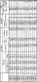
Fig. 7 is the table of expression fault testing fixture, fault kind and defect detection method;
Fig. 8 is that expression calculates the schematic diagram that will form the method for the line of cut position of distinguishing defective region and normal region on the blooming of supplying with;
Fig. 9 is that expression is for the process flow diagram of the method that calculates the position that will form line of cut on the blooming of supplying with;
Figure 10 is that expression is for the process flow diagram of the other method that calculates the position that will form line of cut on the blooming of supplying with;
Figure 11 is that expression is for the process flow diagram of the other method that calculates the position that will form line of cut on the blooming of supplying with;
Figure 12 is that the how to confirm line of cut forms the figure of positional information as utilizing method shown in Figure 9 to carry out the result of computing in expression;
Figure 13 is that the how to confirm line of cut forms the figure of positional information as utilizing method shown in Figure 10 to carry out the result of computing in expression;
Figure 14 is that the how to confirm line of cut forms the figure of positional information as utilizing method shown in Figure 11 to carry out the result of computing in expression;
Figure 15 is the schematic diagram that line of cut forms the position acknowledging device action in the apparatus for continously production of liquid crystal display cells of expression an embodiment of the present invention;
Figure 16 is identification or screen the schematic diagram of the bad diaphragm remover of bad diaphragm action in the apparatus for continously production of liquid crystal display cells of expression an embodiment of the present invention;
Figure 17 be utilize prealignment device, alignment device in the apparatus for continously production of liquid crystal display cells of expression an embodiment of the present invention, to conveying device and each device of liquid crystal panel edge detecting device of applying position and will be transported to by the liquid crystal panel of control attitude the schematic diagram of applying position;
Figure 18 is the figure of the laminating apparatus of normal diaphragm and liquid crystal panel in the apparatus for continously production of liquid crystal display cells of expression an embodiment of the present invention;
Figure 19 is that the recall rate of expression mark that blooming is applied is measured the schematic diagram that employed mark detects test unit;
Figure 20 is the tables by the different expression of shape recall rate of mark that blooming is applied.
Embodiment
In this manual; the film that the one side that fits to liquid crystal panel W of polarizer (polarizer) is formed with adhesive coating is called polarizing coating; described polarizer has diaphragm at single face or two laminateds, will be called " diaphragm of polarizing coating " or only be called " diaphragm " by the diaphragm that the polarizing coating that is commonly referred to as " polarization plates " is configured as rectangle.In addition; in situation about needing from surface protection film and carrier film shape all-in-one-piece polarizing coating shaping diaphragm the time this diaphragm and " diaphragm of polarizing coating " difference; be referred to as " diaphragm of blooming ", will be called " diaphragm of surface protection film " or " diaphragm of carrier film " from surface protection film or the diaphragm that is shaped of carrier film that is contained in wherein.
Below, the embodiment that present invention will be described in detail with reference to the accompanying.
1, the structure of the apparatus for continously production of liquid crystal display cells
Fig. 3 is the skeleton diagram of the apparatus for continously production 1 of expression liquid crystal display cells.Apparatus for continously production 1 comprises: blooming feedway 100, and it is mounted with according to fault (owing a little) information and has executed in advance the laminate roll of tagged blooming (hereinafter referred to as " having executed tagged blooming "); Liquid crystal panel conveying device 300, it will be fitted by the normal diaphragm of executing the polarizing coating that tagged blooming makes of the continuous band-shaped form of supplying with; And control device 400, the action of its control blooming feedway 100 and liquid crystal panel conveying device 300 integral body.Apparatus for continously production 1 comprises: the eliminating station C that gets rid of by the cut-out station A of the diaphragm of executing tagged blooming shaping polarizing coating, with the bad diaphragm of polarizing coating and the applying station B that the normal diaphragm of polarizing coating is fitted to liquid crystal panel.As described later, apparatus for continously production 1 also can and be got rid of station C repeated configuration with applying station B.
Blooming feedway 100 comprises: be used for loading the holder device 110 of having executed tagged optical film laminate reel 10 with rotating freely; Be used for reading the reading device 120 of mark; The film feedway 130 that comprises feed rolls; Be used for the speed adjusting device 140 that includes accumulation of energy roller (ア キ ュ one system ロ one ラ) with the certain speed delivery film; Shearing device 150, it forms line of cut at cut-out station A for blooming is cut; The line of cut that is used for the line of cut position of affirmation formation at same cut-out station A forms position acknowledging device 160; The film feedway 170 that comprises feed rolls; Be used for the speed adjusting device that includes the accumulation of energy roller 180 with the certain speed delivery film; Getting rid of station C for the bad diaphragm remover 190 of the bad diaphragm that will cut off from the carrier film eliminating; Laminating apparatus 200, it comprises a pair of doubling roller, liquid crystal panel is peeled off and fitted to described a pair of doubling roller at the normal diaphragm that applying station B is used for cutting off from carrier film; Batch drive unit 210 for the carrier film of batching carrier film; Edge detecting device 220, it is used for the front end of the normal diaphragm of affirmation polarizing coating at applying station B; And the straight carry detection device 230 of putting for detection of the straight carry of normal diaphragm.Fig. 4 is that expression utilizes that each operation is the process flow diagram of manufacturing step in the liquid crystal display cells manufacturing 1 that these devices carry out.
2, executed the manufacturing of tagged optical film laminate reel
The structure of<blooming 〉
Being installed in the tagged optical film laminate reel 10 of executing of blooming feedway 100 is the laminate rolls that batch flexible blooming, as shown in Figure 1, described flexible blooming comprises: polarizing coating 11, its lamination have on the face that fits to liquid crystal panel of polarizer of diaphragm and are formed with adhesive coating 12; Surface protection film 13, it is freely peeled off the ground lamination on the face that does not have adhesive coating 12 of described polarizing coating 11 and has a bonding plane; And carrier film 14, it freely peels off the ground lamination at the adhesive coating 12 of polarizing coating 11.Laminate roll 10 preferably has the long limit of the liquid crystal panel of being fitted with quilt or the roughly the same width of minor face.In addition, lamination is at the diaphragm on the single face of polarizer or two sides transparent protective film preferably.Carrier film 14 is mold release film, and it protects the adhesive coating 12 of polarizing coating 11 in the manufacturing process of liquid crystal display cells, and it is batched when blooming is peeled off the diaphragm of polarizing coating before fitting with liquid crystal panel or when fitting and removes.Because carrier film 14 has the function as carrier that the normal diaphragm of polarizing coating 11 is transported to applying station B, therefore referred to here as " carrier film ".
Polarizing coating 11 for example forms through following operation.At first, PVA (polyvinyl alcohol) film of 50~80 μ m thickness degree dyeed with iodine and carry out crosslinking Treatment, this PVA film is implemented orientation process to vertical or horizontal extension.Its result arranges iodo-complexes in the direction parallel with the bearing of trend of PVA film, and the polarized light that has vibration in this direction is absorbed, and its result is formed on the successive layers that the direction parallel with bearing of trend has the polarizer of absorption axes.In order to have the polarizer successive layers of superior optical characteristics on the basis that is produced on good homogeneity and precision, the bearing of trend of preferred PVA film is vertical or horizontal consistent with film.In general, polarizer successive layers or to comprise the absorption axes of blooming of polarizer successive layers parallel with the length direction of blooming, polarization axle become vertical with this length direction laterally.The thickness of the successive layers of polarizer is 20~30 μ m.Then, by the diaphragm of bonding agent at the two laminateds protection polarizer successive layers of the polarizer successive layers that forms.General transparent TAC (triacetyl cellulose class) films that use 40~80 μ m thickness degree of diaphragm more.From the viewpoint of liquid crystal display cells slimming, the situation at the one side applying diaphragm of polarizer successive layers is only arranged also.At last, there is the one side of the polarizer successive layers of diaphragm to form the adhesive coating 12 of the acrylic compounds of fitting with liquid crystal panel W in lamination.The thickness of adhesive coating is 10~30 μ m.In addition, the polarizer successive layers following also referred to as " polarizer ".The thickness of polarizing coating 11 is normally about 110~220 μ m.
A wherein side of the diaphragm of polarizing coating 11 can be replaced as the phase retardation film with optical compensation function that uses cycloolefin polymer or TAC base polymer etc.In addition, polarizing coating 11 can also form at the transparent base of TAC class etc. the polymeric materials such as polyesters or polyimide are coated with/be orientateds and immobilized layer.In addition, in the situation as the polarizing coating of fitting to the source backlight of liquid crystal display cells, also can fit to the source diaphragm backlight of polarizer and improve the brightness film and additional function.In addition, about the structure of polarizing coating 11, propose oriented polarizer one side applying TAC film and to various deformation programs such as another side applying PET films.
The polarizing coating that also is not formed for fitting to the adhesive coating of liquid crystal panel W at the single face of polarizer or two laminateds diaphragm being arranged forms one of method of this adhesive coating, but is the method that forms the carrier film 14 of adhesive coating to the laminated transfer printing that fits to liquid crystal panel W of polarizing coating.Concrete printing transferring method is as follows.At first, in the manufacturing process of carrier film 14, the one side of carrier film 14 is implemented the demoulding to be processed, described carrier film 14 laminations are in the face that fits to liquid crystal panel of polarizing coating, the solvent that comprises again bonding agent to the coated on one side of carrier film 14 forms adhesive coating by making this solvent seasoning in carrier film 14.Then, the carrier film that comprises adhesive coating 14 continuous wave outputs that for example will make by with its polarizing coating lamination to same output, and form adhesive coating 12 with the adhesive coating of carrier film 14 to the polarizing coating transfer printing.Also can replace the adhesive coating that forms like this, and the solvent that will comprise bonding agent forms adhesive coating 12 directly to the face coating of fitting with liquid crystal panel of polarizing coating and make its drying.
<executed the manufacturing of tagged laminate roll 〉
The manufacturing method and apparatus of executing tagged optical film laminate reel 10 is described with Fig. 5 and Fig. 6.
Fig. 5 is the schematic diagram of making the device 500 of executing tagged optical film laminate reel 10.Device 500 comprises: make the polarizer manufacturing line (hereinafter referred to as making line) 510 of polarizer successive layers, to the manufacturing line 520 of the diaphragm of polarizer lamination and make line 530; described manufacturing line 530 is by (this is the polarizing coating that does not also form adhesive coating to comprising lamination the polarizing coating of the polarizer of diaphragm being arranged; in order to distinguish with the polarizing coating 11 that is formed with adhesive coating; and be called " polarizing coating 110 ") lamination carrier film 14 and surface protection film 13, make the laminate roll 10 of blooming.Fig. 6 is that each manufacturing process of expression this device 500 is the process flow diagram of manufacturing step.
The manufacturing line 530 of polarizing coating comprises: utilize testing fixture 560 to check the inspection operation of the fault of polarizing coating 110 interior existence; be used for to be formed with the carrier film 14 of transferable adhesive coating 12 to the carrier film supply operation of polarizing coating 110 laminations; be used for across bonding plane surface protection film 13 being had to lamination the surface protection film of laminated of opposition side of the polarizing coating 110 of carrier film 14 to supply with operation; the mark of expression fault information is applied to polarizing coating 110; the marking procedures on surface protection film 13 or carrier film 14 surfaces; and batch the coiling process of executing tagged blooming and forming laminate roll.
Polarizer is made line 510 and is comprised following operation, namely, be mounted for the spool body of the PVA film of polarizer base material with rotating freely, utilize applying drive unit 540 or other not shown drive unit and will dye from the PVA film of spool body output, crosslinked, extend and make its dry operation after processing.Diaphragm is made line 520 and is comprised following operation; namely; be mounted for the spool body of the normally transparent TAC film of diaphragm base material with rotating freely; utilize applying drive unit 540 or other not shown drive unit, and will carry out making its dry operation after the basification from the transparent TAC film of spool body output.The manufacturing line 530 that diaphragm is made line 520 and polarizing coating 110 comprises following operation,, at the bonding agent of the interface of polarizer and diaphragm coating take polyvinyl alcohol resin as host, two films is carried out dry bonding operation with bonding agent that is.
The manufacturing line 530 of polarizing coating 110 has the applying drive unit 540 that comprises a pair of doubling roller.Applying drive unit 540 has measuring motion 550, and this measuring motion 550 will be assembled in arbitrary doubling roller for the scrambler of the output quantity of calculating polarizing coating 110 front ends of making.Doubling roller is crimping polarizer and diaphragm on one side, Yi Bian carry out lamination, makes polarizing coating 110.
In this device 500, after the fault of the surface that detects polarizing coating 110 and inside surface, must form adhesive coating 12 and finish polarizing coating 11 at polarizing coating 110.So this device 500 also comprises the carrier film feedway 570 of the spool body that the carrier film 14 with adhesive coating 12 is installed.Carrier film 14 forms PET (polyethylene terephthalate) film of 20~50 μ m thickness degree in the manufacturing line (not shown) of carrier film in advance as base material.In the one side of carrier film 14, normally after the one side of PET film is implemented demoulding processing, comprise the solvent of acrylic-based adhesives and make its drying to this face coating, make the transferable adhesive coating of 10~30 μ m thickness degree.And by can freely peel off with carrier film 14 come transfer printing to make to polarizing coating 110 laminations adhesive coating, and make the blooming that comprises the polarizing coating 11 that is formed with adhesive coating 12.
This device 500 can also comprise surface protection film feedway 640, and described surface protection film feedway 640 has across the bonding plane lamination surface protection film 13 face of opposition side of the face of carrier film 14 in the lamination of polarizing coating 110.This device 500 has generally included mark bringing device 630, and described mark bringing device 630 is used for after lamination surface protection film 13 and/or carrier film 14, applies mark to the surface of these films.This device 500 comprises that also blooming batches drive unit 580, and described blooming batches drive unit 580 after applying mark by mark bringing device 630, batches blooming.
In the situation of two laminated diaphragms of polarizer, this device 500 comprises that two of diaphragm are made lines 520,520 ' (omitted among Fig. 5 manufacturing line 520 ').Also can be attached to the manufacturing line 520 of diaphragm to polarizer lamination diaphragm and before diaphragm surface (non-lamination face) be applied hard conating processing, anti-dazzle processing or applies the processing processing line that anti-dazzle is processed.
According to the process flow diagram of Fig. 6, in step 1, utilize applying drive unit 540 to make polarizing coating 110 to the single face lamination diaphragm of polarizer.In step 2, Yi Bian the polarizing coating 110 of making is moved, Yi Bian detect the polarizing coating 110 inner faults that exist by testing fixture 560.In step 3, the spool body of carrier film 14 is installed at holder device 571 with rotating freely, in step 4, utilize mold release film to batch drive unit 572 and blooming batches drive unit 580, but the adhesive coating that forms on carrier film 14 transfer printings ground is exposed and from spool body output carrier film 14.In step 5, across adhesive coating and with carrier film 14 can freely peel off to polarizing coating 110 laminations, make the polarizing coating 11 that is formed with adhesive coating 12.
At this, represented and to have formed adhesive coating 12 and freely to peel off the structure that the long-pending carrier film 14 in stratum is carried out simultaneously to this adhesive coating 12 to polarizing coating 11, but also can form adhesive coating 12 to polarizing coating 11 in advance.In addition; particularly with diaphragm before the polarizer lamination; also can whether apply with the surface to diaphragm hard conating processing, non-glare treated or anti-dazzle processes irrelevant; and before step 7, the surface protection film 13 that utilizes the laminating apparatus 640 that arranges in addition will have bonding plane has the laminated of the face opposition side of carrier film 14 to the lamination of polarizing coating 11.Thus, the blooming of finishing just becomes the structure that carrier film 14 and surface protection film 13 are arranged at two laminateds of polarizing coating 11.
As shown in Figure 5 and Figure 6; in the manufacture method of executing tagged optical film laminate reel; with the manufacturing of polarizer and diaphragm as starting point; after the polarizing coating to fitted polarizer and diaphragm carries out the fault inspection; at polarizing coating applying carrier film and/or surface protection film and as blooming, apply mark to the surface of this blooming and batch.But the manufacture method of having executed tagged optical film laminate reel is not limited thereto.In executing other manufacture method of tagged optical film laminate reel; also can after the fault inspection of carrying out polarizing coating, apply mark in the surface (being the surface of diaphragm) to this polarizing coating; then, applying carrier film and/or surface protection film are made and are executed tagged blooming and batch.In executing another manufacture method of tagged optical film laminate reel; also can for example prepare in advance at polarizing coating laminate roll or the laminate roll of carrier film and surface protection film of freely having peeled off the ground lamination of carrier film of freely having peeled off the ground lamination, and with its starting point as manufacturing.In this case; carrier film or carrier film and surface protection film are temporarily peeled off polarizing coating is exposed and carries out after fault checks, again will be same that be stripped from or other carrier film or will be same that be stripped from or other carrier film and surface protection film freely peel off lamination arrive polarizing coating.
Applying of<mark 〉
As shown in Figure 5, this device 500 comprises mark bringing device 630, and described mark bringing device 630 will represent to be detected and be applied to for example carrier film 14 surfaces by the mark of the fault information such as the defect position of signal conditioning package 610 information processings, kind by fault testing fixture 560.Execute the coordinate of Width that tagged position can be set as the blooming that makes this position and length direction and fault and be same position or same position roughly, perhaps making the coordinate of length direction of blooming of this position and fault is same position or same position (namely from blooming laterally, be between defect position and blooming end a certain position) roughly.In addition, so-called " roughly same " refers to following situation, namely, length direction from blooming, execute the difference of position coordinates of the coordinate of tagged position (central portion of mark) and fault preferably in ± 200mm, more preferably in ± 100mm, further preferably in ± 50mm, most preferably in ± 10mm.Although preferably mark is applied to the carrier film 14 that blooming comprises, also can apply to surface protection film 13.
Method for continuous production and device that tagged optical film laminate reel 10 has used liquid crystal display cells of the present invention have been executed.The problem that will solve for the present invention, namely, for Product Precision and manufacturing speed in the continuous manufacturing of rapid raising liquid crystal display cells and the yield rate of significantly improving product, utilize the mark reading device 120 of apparatus for continously production accurately and in short time to detect the mark that is applied to laminate roll just of crucial importance.Therefore, must will have the mark that the mark that can improve mark reading device 120 detects the appropriate feature of precision and be applied to blooming.Detect precision in order to improve mark, can exemplify out shape, thickness, optical concentration, surfaceness of mark etc. as the feature of important mark.
In the present invention, so long as the detection of the mark that has applied can carry out in the apparatus for continously production of liquid crystal display cells reliably, then the shape of mark just without particular limitation of.Preferably mark adopts the mark that such as circle, ellipse, square, rectangle, Long Circle (being also referred to as the fillet rectangle), triangle etc. has simple geometric shape like this.Perhaps, mark also can be set other shape for as required, has like this mark of complicated shape such as aggregate of star or point etc.As described later, with utilizing from the light source irradiation to the mark and the light intensity difference of periphery when coming the mark reading device 120 of certification mark, in order to improve the precision that detects of mark, preferably mark adopts the shape of the circle of being smeared by printing ink, ellipse, square, rectangle, Long Circle, triangle etc.Particularly in order to improve the recall rate of mark, preferably the shape of the mark throughput direction angulation that adopts axle long in the different and described axis of symmetry of two axis of symmetry length of quadrature and blooming less than 45 ° have a symmetric shape of line, shapes such as rectangle, Long Circle, ellipse, wherein, most preferably rectangle, oblong shape.For example, by the ratio (aspect ratio) of suitable adjustment rectangle and oblong lengthwise degree (namely with axis of symmetry in the length of long axle parallel direction) and degree of the growing crosswise length of the short-and-medium axle parallel direction of axis of symmetry (namely with), just can improve the recall rate of mark.Preferably aspect ratio was greater than 1.0: 1, and more preferably aspect ratio was greater than 1.5: 1.In addition, preferably the throughput direction angulation of the axle of length and blooming is more preferably less than 5 ° less than 10 ° in the axis of symmetry of mark, most preferably is approximately 0 °.
Applied that laminate behind the mark is temporarily batched sometimes and as spool body.When the thickness of mark is large, when batching laminate, might produce the distortion that is caused by mark thickness at blooming, become new fault.Therefore, in order not produce this distortion, preferably the thickness of mark is more preferably below the 1.0 μ m below 1.5 μ m.In addition, at this said thickness, for example can utilize light interference type surfaceness meter to measure, be the value of thickness the best part in the digit synbol integral body.
The preferred optical concentration of mark that the present invention uses is more than 2.0.Optical concentration is the absorbance that becomes the wavelength of peak value in the absorbance of various wavelength in the marked region, can measure with small spectrophotometer.Be set in more than 2.0 by the optical concentration with mark, can improve with the light intensity difference of utilizing of the apparatus for continously production 1 that is arranged on liquid crystal display cells and come the mark of the mark reading device 120 of certification mark to detect precision.
Mark is such as applying with the method that is applied by marker, the known methods such as method that applied by ink-jetting style.The thickness of mark can be regulated with the injection pressure that contacts pressure, ink sprayer of blooming or the size of droplet of ink etc. by kind, the marker of marker or the employed printing ink of ink sprayer.
In order to improve the optical concentration of mark, employed ink type when needing suitably to select to apply mark particularly preferably uses the high printing ink of absorptivity.The absorption peak wavelength of mark so long as be arranged on the wavelength that the mark reading device 120 of the apparatus for continously production 1 of liquid crystal display cells can detect, does not just limit, and can be any of visible-range, ultraviolet ray range or infra-red range.In order to improve the precision that detects of mark, preferably the absorption peak wavelength of mark is present in the little wavelength coverage of absorptivity of polarizing coating or blooming.
The mark that is applied to blooming not only can be the information of expression defect position or coordinate, also can be according to kind or the size of fault, for example use by the shape that changes mark, the color that changes mark or the printing ink that the multiple inks that absorbing wavelength is different serves as a mark, and have the kind of fault or the various information relevant with fault such as size of fault so that be applied to the mark of blooming.
3, the continuous manufacturing of liquid crystal display cells
The installation of<laminate roll and output 〉
Above-mentioned such make execute the blooming feedway 100 that tagged optical film laminate reel 10 is installed in liquid crystal display cells apparatus for continously production 1 of the present invention, export as the blooming of continuous band-shaped form.Preferably the holder device 110 at blooming feedway 100 is provided with the scrambler (not shown) of surveying long data for calculating according to the output quantity of blooming, and the survey long data that utilizes this scrambler to calculate is stored in the memory storage 420 of control device 400.The calculating of the survey long data of blooming also can be undertaken by the measurement mechanism that is arranged in addition blooming feedway 100.
Detecting of<mark 〉
The mark that applies for the blooming from holder device 110 outputs is detected by mark reading device 120.As shown in Figure 3, in one embodiment of the present invention, mark reading device 120 comprises: be arranged on the light source 121 of the top or following either side of blooming, blooming is clipped in the middle and is arranged on video camera 122 and the controller 123 of light source 121 opposition sides.Light source 121 can adopt the light source of emission visible light, also can be emission beyond the visible light ultraviolet light or the light source of infrared light.Video camera 122 can possess the imaging apparatuss such as lens, CCD or CMOS, and it can catch according to the kind of light source 121 the light both sides beyond any or visible light and the visible light of light beyond visible light or the visible light.
From the irradiation of light source 121 emission on the mark that blooming is applied and on the blooming of mark periphery.The part of the light of irradiation is absorbed according to the optical concentration of mark, and a remaining part is not labeled absorption and incides video camera 122 through blooming.The light that incides video camera 122 is converted to the electric signal of respective light intensities by imaging apparatus, this information is that the image of mark and mark periphery is sent to controller 123.Controller 123 converts the information of the light intensity of correspondence markings and periphery thereof to for example black and white 256 gray scales.
Controller 123 computings are applied in gray scale and the mark periphery of mark part and namely do not execute the poor of tagged blooming gray scale partly.Execute tagged part on the blooming, owing to being labeled absorption from the light of light source 121, therefore, see through mark part and the light that incides video camera 122 dies down.On the other hand, the periphery of mark is not namely executed tagged part, because from most of transmission optics film of the light of light source 121, therefore sees through this part and the light ratio that incides video camera 122 sees through the light intensity of mark part.Owing to see through the poor of the light intensity be applied with mark part and the light intensity that sees through the mark periphery, so the generation of the gray scale of mark part and its periphery is poor, by the size of this difference judge have on the blooming unmarked.Controller 123 compares gray scale difference and the predefined threshold value of computing, in the situation that gray scale difference is larger than threshold value, judges that then the little part of transmitted intensity is exactly to execute tagged part.In the gray scale difference of the computing situation less than threshold value, then controller 123 is judged on blooming corresponding to the image section of obtaining with video camera 122 and is not applied mark.Threshold value can suitably be set according to the characteristic of mark and the characteristic of light source 121 and video camera 122.If it is too much that the value of threshold value is set, then the recall rate of mark reduces, if the value of threshold value is set too smallly, the mark recall rate that then optical concentration is low improves, but the possibility that the flase drop that causes owing to noise goes out uprises.
Represent in Fig. 3, the light source 121 of mark detecting apparatus 120 is positioned at the downside of blooming, and video camera 122 is positioned at the upside of blooming.But also light source 121 and video camera 122 can be configured the top or following same side that Chengdu are positioned at blooming.At this moment, incide that the light intensity of video camera 122 is poor just to become the poor of light from light source 121 light intensity that is applied in the mark part reflection and the light intensity that is not applied the mark part reflection, and the threshold value of this difference and regulation is compared.Controller 123 can consist of with video camera 122 one, also can constitute to be included in the control device 400.
<line of cut forms the computing of position 〉
When controller 123 is judged as when blooming corresponding to the image of obtaining with video camera 122 partly is applied in mark, then according to detected label information, that obtains the line of cut that applied at blooming by shearing device shown in Figure 3 150 should form the position.Line of cut formation position for example forms position arithmetic element 415 by the lines of cut in the signal conditioning package 410 that is assembled in control device 400 and comes computing.Line of cut forms position arithmetic element 415 according to the survey long data of detected mark position or coordinate and blooming, and as follows, computing is to the formation positional information of the film formed line of cut of optics.It is to specify the information that form the position of line of cut to blooming that line of cut forms positional information, the following formation of line of cut, namely, when making liquid crystal display cells, by the throughput direction edge horizontal degree of depth of from the opposition side of carrier film this blooming being cut and cut the face of the adhesive coating side that reach carrier film of shearing device 150 with respect to the blooming that is supplied to, and form line of cut.This cutting line forming method is also referred to as hemisect.The line of cut that generates forms positional information and is stored in memory storage 420.
Including in side this formed zone of line of cut of two of line of cut of leaving predetermined distance downstream by the line of cut of the upstream side of blooming with from this line of cut: the normal region of polarizing coating, the normal region of described polarizing coating have the given size length of being determined by the length on the limit of the liquid crystal panel of fitting and do not comprise fault; And the defective region of polarizing coating, the defective region of described polarizing coating is usually short than given size length and comprise fault.By the defective region of shearing device 150 by the formed polarizing coating 11 of two place's lines of cut, become the bad diaphragm X β that is got rid of from blooming (being carrier film 14 specifically) by bad diaphragm remover 190.Equally, the normal region is for being peeled off and fitted to by laminating apparatus 200 the normal diaphragm X α of liquid crystal panel one side from blooming (being carrier film 14 specifically).
Fig. 8 is that expression calculates the schematic diagram that will form the method for the line of cut position of distinguishing defective region and normal region at the blooming of supplying with.Fig. 9~Figure 11 is that expression is used for calculating the process flow diagram that will form the distinct methods of line of cut position on the blooming of supplying with.In addition, Figure 12~Figure 14 is that the how to confirm line of cut forms the figure of positional information as utilizing these distinct methods to carry out the result of computing in expression.
Below, illustrate that with Fig. 8~Figure 14 line of cut forms the operational method of positional information.At first, export blooming in the step 1 of Fig. 9.At this moment, the output quantity according to blooming obtains surveying long data.In step 2, detect the mark that blooming is applied by mark reading device 120.Signal conditioning package 410 calculates position or the coordinate of mark according to the survey long data of the mark that detects and blooming.The position of mark or the information of coordinate are stored in memory storage 420.In another embodiment of the present invention, the kind by changing the mark that blooming is applied, color etc. also can make mark self have the position of fault or the information beyond the coordinate, such as the kind of fault, the information such as size of fault.In this case, the label information that signal conditioning package 410 detects according to mark reading device 120 is not only obtained position or the coordinate information of fault, and obtains the information such as the kind of fault or size, and stores this information into memory storage 420.
Then, in step 3 and step 4, line of cut forms position arithmetic element 415 according to the mark position or the coordinate that detect, comes the length of diaphragm of comparison blooming and the length x α suitable with the normal region.At first, in step 3, line of cut form position arithmetic element 415 computings from a certain position of blooming (for example Fig. 8, the position that represents as A.Be that the first line of cut forms the position with this set positions) to the distance X of mark position.Then in step 4, line of cut forms position arithmetic element 415 computings and deducts the distance (X-x α) of the length x α suitable with the normal region=X ' from distance X.The length x α suitable with the normal region of blooming set and pre-stored at memory storage 420 by system operator according to the size of liquid crystal panel.Then, line of cut forms position arithmetic element 415 and judges the distance X that calculates ' larger or little at the length x α suitable with normal region blooming memory storage 420 than pre-stored.
When X ' shown in Figure 8>x α, then can guarantee the normal region X α of blooming.Therefore, line of cut formation position arithmetic element 415 forms position (the second line of cut forms the position) next definite (step 6) with the position B that the upstream side from position A (the first line of cut formation position) to blooming leaves x α as the next line of cut that is used to form the normal diaphragm X α suitable with the normal region of blooming.Equally, line of cut forms position arithmetic element 415 and calculates the length that deducts the length x α suitable with the normal region from the second line of cut formation position B, when this Length Ratio x α is large, the position C that then upstream side from the second line of cut formation position B to blooming is left x α forms the position as the 3rd line of cut and determines, and then similarly next position D is determined as the 4th line of cut formation position.
On the other hand, when X '≤x α, i.e. X shown in Figure 8 " '≤during x α, then can't guarantee the normal region X α of blooming.At this moment, line of cut forms 415 couples of X of position the arithmetic element " ' size x0 that adds regulation calculate the length suitable with defective region X β (X " '+X0)=x β.That is, to leave the position E of x β be that the line of cut that is used to form the bad diaphragm X β suitable with the defective region of blooming forms position (step 6) to the upstream side from position D to blooming.
In sum, line of cut forms position arithmetic element 415 and carries out following (a) and computing (b) according to the label information that is read by mark reading device 120 with by the survey long data that the blooming output quantity calculates, namely
(a) when X '>x α, to the distance that will form next line of cut position=x α
(b) when X '≤x α, to the distance that will form next line of cut position=(X '+x0)=x β, with this location positioning for forming the position (step 6 of Figure 10) of next line of cut.
Yet, when the result who is formed position arithmetic element 415 by line of cut and carry out computing is following situation, namely, the length suitable with defective region (X '+x0)=x β be the length x α suitable with the normal region equate value the time, namely (X '+x0)=during x α, signal conditioning package 410 None-identifieds or filter out normal region X α and defective region X β then.That is, owing to defective region can not be identified as defective region X β, therefore, think that it is that signal conditioning package 410 can not be judged this zone for which of normal region X α or defective region X β.With the supposition of this situation be, the situation of the position of the fault that exists in the blooming or the position that will form next line of cut of coordinate infinite approach blooming, or spread all over the situation of fault continuous distribution on the length x α suitable with the normal region.Therefore, (X '+x0)=during x α, preference information treating apparatus 410 carries out information processing according to following either method at least, can identify or filter out normal region X α and defective region X β.
In the situation that above-mentioned (b), though by line of cut form that position arithmetic element 415 calculates to the distance that will form next line of cut position (X '+x0) be the length x α suitable with the normal region, this zone neither normal region X α.In order to identify this situation, in one embodiment of the present invention, shown in the step 5 of Fig. 9, make the data that represent respectively normal region and defective region form positional information with line of cut and be associated.For example, become in the result that line of cut forms position arithmetic element 415 computings (X '+x0)=situation (namely having markd situation between two lines of cut) of x α under, as shown in figure 12, signal conditioning package 410 will represent that the value x γ of defective region=1 and this line of cut form position or its previous line of cut and form the some of position and be associated.On the other hand, be in the situation of X '>x α in addition situation, signal conditioning package 410 will represent that the value x γ of normal region=0 and this line of cut form position or its previous line of cut and form the some of position and be associated.In addition, in the situation that x β<x α, the value x γ of expression defective region=1 is associated with line of cut formation position.
In another embodiment of the present invention, calculate be the length x α suitable with the normal region to the distance that will form next line of cut position (X '+x 0) time, shown in the step 5 of Figure 10, line of cut forms position arithmetic element 415 and revises operation results to form the position of next line of cut become (X '+x 0 ') (x 0 '>x0).As shown in figure 13, the method is by calculating the x β different from x α=(X '+x 0 '), and length areas that can identify or filter out (X '+x 0 ') is defective region X β and normal region X α.
In another embodiment of the present invention, the distance to the position that will form next line of cut that calculates (X '+when x0) becoming the length x α suitable with the normal region, shown in the step 5 of Figure 11, line of cut forms position arithmetic element 415 and revises operation result, so that to form the position of next line of cut become (X '+x0)/m (m is more than 2, preferably 2 or 3).As shown in figure 14, the method by calculate the x β different from x α=(X '+x0)/m, and can identify or filter out (X '+x0)/length areas of m is defective region X β and normal region X α.
In sum, the present invention for example can use following either method as generating the method that is used for identification or filters out the information of defective region and normal region.
(1) as be used for identification or filter out (X '+method of the defective region X β of x0) length and the Information generation x γ of normal region X α
(2) generate different from the x α methods to the distance=X ' that will form next line of cut position+x0 ' (x 0 '>x α)
(3) generate different from x α to the distance that will form next line of cut position=(X '+x0)/method of m (m is more than 2)
Particularly in the situation of the method that adopts (2) or (3), (X '+x0)=x α, but by line of cut form result that position arithmetic element 415 revises be become (X '+x0 ') ≠ x α or (X '+x0)/m ≠ x α, therefore, these lines of cut that will form line of cut form positional information self as information (information that is equivalent to the x γ in (1) method) the performance function of expression normal region X α and the defective region X β that is identified or screens.
After having determined that line of cut forms the position, then in step 7, in the situation that (1), the length that forms the position to next line of cut that will be determined by signal conditioning package 410 is associated with information x γ and stores memory storage 420 into.In the situation that above-mentioned (2) or (3), will store memory storage 420 in the length that forms the position to next line of cut that step 6 is determined by signal conditioning package 410.
The formation of<line of cut 〉
After detecting mark by mark reading device 120, blooming is sent to and cuts off station A.Shearing device 150 bases of cutting off station A form the survey long data that arithmetic element 415 definite lines of cut in position form positional information and blooming by line of cut, form line of cut (that is, shearing device 150 is with the blooming hemisect) at blooming successively.As shearing device 150 such as using the known devices such as laser disconnecting device, cutting tool device.
<line of cut forms the affirmation of position 〉
In cutting off station A, shearing device 150 laterally successively forms line of cut at blooming with respect to its throughput direction edge according to the information that will form the line of cut position.If but the position of the line of cut that forms successively is inaccurate, then be difficult to improve the Product Precision of liquid crystal display cells.Therefore, in the apparatus for continously production and method of liquid crystal display cells, it is important that line of cut is formed on the blooming exactly.
Figure 15 is the schematic diagram that the expression line of cut forms position acknowledging device 160 actions.Line of cut forms position acknowledging device 160 and comprises affirmation: on the blooming with respect to its throughput direction along the physical location of the line of cut that laterally forms, and to form deviation between the line of cut position according to what mark was formed by line of cut that position arithmetic element 415 calculates.From the throughput direction of blooming, it is shearing device 150 is clipped in the middle and is arranged on upstream side and downstream that line of cut forms position acknowledging device 160.The more downstream that line of cut in the downstream forms position acknowledging device 160 is provided with the film feedway 170 that comprises feed rolls, utilizes this film feedway 170, makes the supply of the blooming that stops of short duration when forming line of cut begin to carry out again.On the other hand, the more upstream side that forms position acknowledging device 160 at the line of cut of upstream side is provided with the speed adjusting device 140 that comprises the accumulation of energy roller, utilize this speed adjusting device 140, even the conveying of blooming is temporarily stopped when forming line of cut, also can keep the supply of the blooming that is undertaken by the film feedway 130 that comprises feed rolls.
Affirmation with respect to the throughput direction of blooming along the line of cut position that laterally forms with whether formed the position that will form line of cut that position arithmetic element 415 calculates by line of cut consistent, flow direction (directions X) that can be by obtaining blooming and the accurate location of transverse direction (Y-direction) carry out.Preferably confirm following carrying out, that is, clip in front and back by measuring that line of cut forms the formation position of two actual lines of cut in position of position and (side end) position, blooming edge and the directions X between the datum line of position and the deviation of Y-direction are carried out above-mentioned affirmation separately.For example, utilizing the line of cut comprise ccd video camera to form marginal position that position acknowledging device 160 comes line of cut to blooming to form position and blooming takes and carries out image conversion.In coverage, set in advance datum line separately.Datum line is expression is formed the position that will form line of cut that position arithmetic element 415 calculates by line of cut line.The line of cut of blooming forms the interior poor contrast of image of the marginal position utilization shooting of position and blooming and judges.Then, calculate the distance (deviation) that predefined datum line and line of cut form the marginal position of position and blooming, revise position and the angle of shearing device 150 according to the distance that calculates (deviation).
Specifically, the inspection of the deviation between the position that will form line of cut definite with formed position arithmetic element 415 by line of cut, the line of cut position that confirm to form is undertaken by step shown below as an example.
(1) marginal position that utilizes the line of cut that comprises ccd video camera to form 160 pairs of lines of cut formation positions of position acknowledging device and two positions is taken, and utilizes the poor contrast in the image to obtain line of cut position X and marginal position Y1, Y2.
(2) in the line of cut of seeing upstream side from directions X forms the coverage of position acknowledging device 160 the predefined datum line that extends along Y-direction, form the centre position of the predefined datum line that extends along Y-direction in the coverage of position acknowledging device 160 with the line of cut of seeing the downstream from directions X, preset the line of cut that extends along Y-direction and form reference position 165, be stored in advance in memory storage 420 apart from γ between upstream side datum line and the downstream datum line.In addition, in the coverage of the line of cut formation position acknowledging device 160 of seeing the downstream from directions X, preset the datum line that extends along directions X.
(3) form position X and marginal position Y1, Y2 and said reference line according to the line of cut of obtaining, calculate line of cut and form the correction amount alpha of position and the correction δ of line of cut angulation.The correction amount alpha that line of cut forms the position is the departure α that measures, namely be line of cut form position X and downstream along the departure α between the datum line of Y-direction extension.The correction δ of line of cut angulation be according to apart from the departure at two positions of the Y-direction of the range observation of blooming marginal position namely between departure β 1, the β 2 of the downstream datum line that extends along directions X of distance and upstream side datum line and two datum lines apart from γ, and can utilize following formula to calculate.
[formula 1]
(4) according to the data that calculate, for consistent with the datum line of the line of cut formation position of extending along Y-direction, make the position correction of the α amount of the angle modification of δ amount and directions X become correction amount alpha and δ to shearing device 150 indications, and to memory storage 420 storages.
(5) shearing device 150 when forming next line of cut, according to making the line of cut mode consistent with datum line, carries out the correction angle modification horizontal with relative throughput direction of throughput direction according to correction amount alpha and the δ of storage.
(6) last, shearing device 150 carries out work and forms next line of cut at blooming.
The eliminating of<bad diaphragm 〉
After forming line of cut by shearing device 150, blooming is sent to gets rid of station C.Freely peeling off the ground lamination on the carrier film 14 that is sent to the blooming of getting rid of station C has normal diaphragm X α and the bad diaphragm X β of the polarizing coating 11 that is cut the line cut-out.Get rid of bad diaphragm remover 190 identifications of station C or filter out the bad diaphragm X β that blooming comprises, and it is peeled off eliminating from carrier film 14.Bad diaphragm remover 190 is according to the identifying information such as Fig. 9 and bad diaphragm shown in Figure 12, being different from normal diaphragm only identifies bad diaphragm X β or filter out, perhaps such as Figure 10, Figure 11, Figure 13, shown in Figure 14, according to the length of normal diaphragm X α and bad diaphragm X β, also can identify or filter out bad diaphragm X β.Figure 16 (1) and Figure 16 (2) expression identification or filter out bad diaphragm X β and the bad diaphragm remover 190 that moves.
The bad diaphragm remover 190 of Figure 16 (1) comprises: illusory film drive unit 191, and it has to paste freely peels off the ground lamination at the bad diaphragm X β of carrier film 14 and with its function of peeling off from carrier film 14; And mobile device 192, it moves when bad diaphragm X β arrives the eliminating starting point of blooming carrying path.Mobile device 192 is blooming is moved and engage the device that breaks away from the illusory film carrying path of illusory film drive unit 191.
The bad diaphragm remover 190 of Figure 16 (2) is at the device of applying station B with the laminating apparatus 200 interlocks action that comprises a pair of doubling roller, comprise: illusory film drive unit 191, it has pastes bad diaphragm X β and with its function of peeling off from carrier film 14; And mobile roller 192, it consists of the illusory film carrying path of this illusory film drive unit 191.The difference of the device of the device of Figure 16 (2) and Figure 16 (1) is, the device of Figure 16 (2) is in applying station B, makes a pair of doubling roller that comprises with laminating apparatus 200 approach the mobile roller 192 of the illusory film carrying path of formation that configures and the doubling roller interlock of laminating apparatus 200.Specifically, at applying station B, control device 400 arrives the carrying path terminal point of blooming when (namely getting rid of starting point) at bad diaphragm X β, a pair of doubling roller is broken away from, and then the mobile roller 192 that makes the illusory film carrying path of formation moves to the gap between the doubling roller that leaves, by with the mobile roller 192 roller displacement with a side of doubling roller, and make mobile roller 192 and the opposing party's of doubling roller roller interlock.At this moment, batch carrier film 14 owing to utilizing carrier film to batch drive unit 210, therefore, bad diaphragm X β is peeled off from carrier film 14, the bad diaphragm X β utilization that is stripped from is attached to illusory film carrying path with the mobile roller 192 of the opposing party's of doubling roller roller interlock, is excluded.
The conveying of<liquid crystal panel and with the applying of normal diaphragm
Shown in Figure 16 (1), be removed at the bad diaphragm X of eliminating station C β, next the blooming that only has normal diaphragm X α on carrier film 14 is sent to applying station B.In another embodiment of the remover that adopts Figure 16 (2), the blooming that is formed with normal diaphragm X α and bad diaphragm X β in carrier film 14 is sent to applying station B.At this, the former embodiment has illustrated the applying of liquid crystal panel and normal diaphragm X α, and the latter's embodiment is except getting rid of bad diaphragm X β at applying station B, then with the former embodiment identical.Figure 17 be expression utilize the included prealignment device 310 of liquid crystal panel conveying device 300, alignment device 320, to conveying device 330 and liquid crystal panel edge detecting device 340 each device of applying position, will have been controlled the figure that the liquid crystal panel W of attitude carries to the applying position.In addition, Figure 18 represents the laminating apparatus 200 of normal diaphragm X α and liquid crystal panel W, and it comprises: detect normal diaphragm X α front edge part edge detecting device 220, carrier film 14 is acutangulated the peel plate 211 of peeling off from normal diaphragm X α.
Liquid crystal panel W is taken out from the hopper of accommodating a plurality of liquid crystal panels one by one by feedway, through for example cleaning/grinding, as shown in figure 17, utilize conveying device 300 to be adjusted to certain intervals and certain speed, be transported to the laminating apparatus 200 of applying station B.As shown in figure 17, conveying device 300 comprises: by prealignment device 310, alignment device 320, to the conveying device 330 of applying position, detect the liquid crystal panel attitude-control device that the edge detecting device 340 of liquid crystal panel W front edge part consists of.When normal diaphragm X α was delivered to applying station B, the attitude of liquid crystal panel W was synchronously controlled in the conveying of conveying device 300 and normal diaphragm X α.
Preferably the normal diaphragm X α transporting velocity on the carrier film 14 is adjusted to the laminating apparatus 200 that necessarily is fed into applying station B.As shown in Figure 17 and Figure 18, at applying station B, peel off normal diaphragm X α by utilizing peel plate 211 to make carrier film 14 form acute angle.By making carrier film 14 form acute angles, and the adhesive coating of normal diaphragm X α is exposed gradually.Its result exposes the front edge part of normal diaphragm X α a little, easily carries out the marginal portion of front end and the front edge position alignment partly of liquid crystal panel W.
The front edge of normal diaphragm X α partly appears at the gap location of a pair of doubling roller when above-below direction breaks away from of laminating apparatus 200.Normal diaphragm X α is transferred with the state of lamination in carrier film 14, but becomes situation that 0 mode carries exactly seldom according to the angle θ of the throughput direction of the length direction of relative carrier film 14.So, by the ccd video camera that for example utilizes edge detecting device 220 and straight carry detection device 230 normal diaphragm X α is taken and image conversion, thus, use length direction apart from x, calculate the throughput direction of normal diaphragm X α and horizontal deviation with the distance y of the direction of length direction quadrature and the angle θ of relative length direction.
On the other hand, liquid crystal panel W is supplied with certain speed at certain intervals successively from conveying device, the liquid crystal panel W that is carried one by one controls attitude by liquid crystal panel conveying device 300 shown in Figure 17.With reference to Figure 17 this attitude control is described.
By prealignment device 310 with liquid crystal panel W in turn make its vertical and horizontal and the throughput direction of carrying path and with it the direction of quadrature align, substantially position.Then, liquid crystal panel W is transported to the alignment device 320 of the alignment tool 321 that comprises rotation.The front edge part that is loaded onto the liquid crystal panel W of alignment tool 321 is detected by edge detecting device 340.Being compared in the position of front edge part and the benchmark applying position of memory storage 420 storages, is exactly to compare with the x, the y that use the normal diaphragm X α attitude of expression, the data that θ calculates specifically.For example, use the alignment mark of liquid crystal panel W shown in Figure 2, measure the position deviation amount between its position and the benchmark applying position, computing deviation angle θ makes alignment tool 321 rotational angle θ.Then, alignment tool 321 is connected with conveying device 330 to applying station B.Liquid crystal panel W utilization is delivered to laminating apparatus 200 to the conveying device 330 of applying station B with the attitude of former state, make the front edge part of liquid crystal panel W overlapping with the front edge part position alignment of the normal diaphragm X α of polarizing coating.At last, normal diaphragm X α and the liquid crystal panel W of position alignment utilized a pair of doubling roller crimping, thereby finish liquid crystal display cells.
Method and apparatus of the present invention, because utilizing the blooming supplied with tensioning state, normal diaphragm x α is fed into laminating apparatus 200 with liquid crystal panel W with carrier film 14 with being integral, therefore, the circumferential edges of normal diaphragm x α is not flexible or sagging, therefore, normal diaphragm x α can not produce deflection or warpage.Therefore, easily make the attitude of liquid crystal panel W consistent with the normal diaphragm x α that is sent to applying station B, can make liquid crystal display cells make high speed and liquid crystal display cells high precision int.Such method and apparatus, in following situation, eventually can not adopt, namely, as monolithic type diaphragm manufacturing method and apparatus, after the monolithic type diaphragm peeled off barrier film one by one adhesive coating is exposed, and its absorption is transported to applying position with liquid crystal panel W, with liquid crystal panel W position alignment, overlap to fit and finish the situation of liquid crystal display cells.
4, embodiment
The embodiment of the mark recall rate that blooming is applied below is described.
<blooming 〉
The film that the employed blooming of the present embodiment uses is (Ri East Electricity worker Zhu formula Hui She System VEG1724DU: the VEG1724DU of Nitto Denko Corp's system) film; this film is by making polarizing coating by the transparent diaphragm of two laminateds of the polarizer that is consisted of by the polyvinyl alcohol film of iodine staining; one side at this polarizing coating arranges the acrylic compounds adhesive coating, and lamination is coated with the carrier film (barrier film) that is made of the polyethylene terephthalate film of silicon class remover on adhesive coating.
Applying of<mark 〉
Blooming with using the clamping driven roller to export with the transporting velocity of 10m/min or 20m/min from the stock reel that is wound with above-mentioned blooming is directed on the backing roll that arranges with the 200mm interval.At this moment, the mode passed through from the backing roll with its carrier film side of blooming is transferred.The face that does not have adhesive coating at the blooming that is transferred like this is to be applied with mark by marker on the diaphragm.Marker is by on the retainer that is arranged on the driver front end that is driven by servomotor, and it utilizes the action of driver and moves up and down.The surface that the front end of marker is adjusted to distance protection film when applying mark is-height of 5mm (, the front end by marker contact with diaphragm the difference of height and the height of the diaphragm that passes through from the backing roll periphery of the surperficial recessed point that makes diaphragm become-5mm).Marker and diaphragm surface angulation are adjusted to 60 °.Applying mark can carry out various changes with the ratio (aspect ratio) of its longitudinal length (with the length of the throughput direction parallel direction of blooming) and lateral length (length of the throughput direction transverse direction of relative blooming) and apply on blooming.The longitudinal length of the mark that applies, lateral length and aspect ratio are as shown in figure 20.
The employed marker of embodiment and comparative example has following three kinds, and aspect ratio and the print speed printing speed of the mark that is applied by various markers are illustrated in Figure 20.
A: ス テ Star De ラ one System (thinking platform Duola system) marker (trade name " one (deceiving) of Le モ カ ラ ": trade name " luminous colour (deceiving) ")
B: シ ャ チ ハ タ System (system is answered in lower its Kazakhstan) marker (trade name " profit core (deceiving) ": trade name " profit core (deceiving) ")
C: パ ィ ロ Star ト She System (pioneer company system) marker (trade name " V ス one パ one カ ラ one (deceiving) ": trade name " the super colour of V (deceiving) ")
The mensuration of<mark thickness 〉
From executing tagged blooming barrier film peeled off by above-mentioned A~C marker, with it via bonding agent and utilize the hand roller to paste the smooth glass (System of MATSUNAMI society: Song Bo company system), use light interference type surfaceness meter (System of Veeco society (Veeco company system) WYKO NT9800) to measure the surface configuration of mark of 50mm * 100mm.Condition determination is as follows.
Datum line: the label side surface that is set in blooming
Back Scan (from datum line to the higher limit of measuring height): 30 μ m
Scan Length (distance from the maximum height to the lower limit): 40 μ m
Modulation Threshold (catoptrical luminous sensitivity): 0.1%
Stitching (measurement range): X=25mm, Y=8mm
According to the surface configuration data that obtain obtain from the mid point of the long axis direction of mark by and with the area in the cross section of long axis direction quadrature, the serve as a mark thickness of central portion of the value that this area of section is removed with the base length in mark cross section.The thickness of various marks as shown in figure 20.
The mensuration of<optical concentration 〉
To execute tagged blooming by above-mentioned A~C marker utilizes masking tape (a day East Electricity worker strain formula can the System N0.7253 of society: the smooth glass (System of MATSUNAMI society: Song Bo company system) that day Dong Diangongshe N0.7253 processed) pastes 50mm * 100mm, use small spectrophotometer (Lambda Vision She System (company's system) LVmicro) to measure the absorption spectrum of the tiny area of mark, with the peak value of absorbance as optical concentration.Condition determination is as follows.
Light source: halogen heavy hydrogen light source
Pinhole size: φ 100 μ m
Sensor: Multidetector
Measurement pattern: transmissivity mode determination
The optical concentration of various marks as shown in figure 20.
The mensuration of<mark recall rate 〉
The recall rate of Figure 19 summary expressive notation is measured employed mark and is detected test unit.Mark detects test unit and comprises: install the laminate roll 2101 of executing tagged blooming F roller pallet 2102, be used for batching the roller pallet 2103 of the blooming F of output, for detection of the mark detecting apparatus 2104 of the mark that is applied in and a plurality of rollers 2105 of support of optical film.Mark detecting apparatus 2104 comprises: (Electricity leads to Chan Ye System FL48/800W85-DF to light source: the logical industry FL48/800W85-DF processed of electricity) 2104a, video camera (キ one worker ン ス System CV-200M: section is along silk CV-200M processed) 2104b, controller (キ one worker ン ス System CV-2000: section is along silk CV-2000 processed) 2104c.
Following the carrying out of detection test of mark.At first, prepare the above-mentioned blooming of width 400mm, length 200m, utilize above-mentioned A~C marker to apply mark to the diaphragm surface (that is the face that, does not have adhesive coating) that it exposes.Various marks shown in Figure 20, the quantity of mark are respectively 100.Execute tagged blooming F as laminate roll 2101 coilings and be installed to mark and detected test unit.To execute tagged laminate roll 2101 and apply tension force and be arranged between roller pallet 2102 and the roller pallet 2103, and divide with transporting velocity 5.0m/ blooming F is batched to roller pallet 2103 from roller pallet 2102.The mark that is applied to blooming F is detected by mark detecting apparatus 2104.Detected by video camera 2104b from the optical transmission light of light source 2104a emission, the intensity information that incides video camera is transformed into black and white 256 gray scales by controller 2104c.Controller 2104c will apply gray scale difference that the difference of the light intensity of the light intensity of mark part and transmission mark periphery produces and the threshold value of regulation compares owing to transmission, when difference is larger than threshold value, then judge to have applied mark.Threshold value is made as 150 in the present embodiment.
The recall rate that the mark that Figure 20 represents blooming is applied represents by the shape difference.In addition, Figure 20 also expresses owing to the bad generation quantity of scar that applies the blooming that mark causes.The following mensuration of the bad generation quantity of scar.At first, various marks shown in Figure 20 are applied for above-mentioned blooming (width 400mm * length 1100m) by every 2m, apply 100N tension force and batch and become reel while will execute tagged blooming.With this reel with 40% keeping of 23 ℃ of temperature, relative humidity after one month, cut into given size by the length of 700mm, take not execute 1000 in tagged sample, confirm the bad generation quantity of scar with visual.
(1) comparative example 1 and comparative example 2 are the results when changing the mark aspect ratio with respect to embodiment 1~embodiment 4.The mark of embodiment 1~embodiment 4 is vertical than laterally long rectangular shape, and with respect to this, the mark shape of comparative example 1 and comparative example 2 is roughly square.Can find out that foursquare mark compares with rectangular mark, then the recall rate of mark reduces.
(2) comparative example 3 and comparative example 4 are the results when changing the mark optical concentration with respect to embodiment 1~embodiment 4.Can find out from this result, even shape is rectangle, its recall rate of mark that optical concentration is low reduces.
(3) comparative example 5~comparative example 10 is the results when changing marker with respect to embodiment 1~embodiment 4.The mark of comparative example 5 and comparative example 6 has the rectangular shape same with the mark of embodiment 1~embodiment 4, and optical concentration is also high.Therefore, recall rate is 100%.But because the thickness of mark is larger, and the bad generation quantity of scar is very many, in the situation that use these marks, the yield rate of product significantly reduces.
(4) mark of comparative example 7~comparative example 10 has the rectangular shape same with the mark of embodiment 1~embodiment 4, but optical concentration is low.Therefore, the recall rate that can find out these marks reduces.
Result according to Figure 20, shape by suitable selected marker, and make optical concentration become the above labelling apparatus of appropriate value, can the continuous manufacturing of tremendous raising liquid crystal display cells in Product Precision and manufacturing speed, significantly improve the yield rate of product.
The present invention has put down in writing preferred embodiment, but to those skilled in the art, can know not break away from the scope of the invention and can carry out various changes, can replace associated mechanism by equivalent.Therefore, the present invention be not limited to for implement that the present invention considers as the disclosed specific implementations of preferred implementation, the meaning is to comprise all embodiments that belong to the technical scheme scope.
Claims (13)
1. the method for continuous production of a liquid crystal display cells, to fit and continuously manufacturing liquid crystal display element from blooming cuts out the polarizing coating of formation as the diaphragm of specified length diaphragm and liquid crystal panel, described blooming is the blooming of continuous band-shaped form, it comprises: comprise the polarizing coating of adhesive coating and the carrier film that lamination also can freely be peeled off at described adhesive coating, described blooming has the width corresponding with the long limit of liquid crystal panel or minor face, the method for continuous production of described liquid crystal display cells is characterised in that, comprises the steps:
Described blooming is exported to off-position continuously;
Measure the output quantity of described blooming, calculate the survey long data according to described output quantity;
Come certification mark while the position that described blooming was moved before arriving described off-position, described mark represents to be detected and be applied in advance by precheck the defect position of the described polarizing coating of described blooming;
According to detected described mark and described survey long data, come to determine to form with respect to the throughput direction of the described blooming position along the line of cut of the described blooming of right angle orientation crosscut;
According to the described position that will form described line of cut, in described off-position, form successively described line of cut from a side opposite with described carrier film according to the degree of depth of the face of the adhesive coating side that arrives described carrier film;
The diaphragm of the described polarizing coating that judgement is divided by described line of cut is applied with the bad diaphragm of described mark or does not apply the normal diaphragm of described mark;
The diaphragm that is judged as normal diaphragm at described determining step among the diaphragm of the described polarizing coating that will be divided by described line of cut is peeled off from described carrier film; And
According to the mode with the described normal diaphragm position alignment that is fed into the applying position liquid crystal panel is supplied to described applying position, described normal diaphragm and described liquid crystal panel are fitted.
2. the method for continuous production of liquid crystal display cells as claimed in claim 1 is characterized in that,
In the length of the throughput direction of described bad diaphragm with the described equal in length of described liquid crystal panel or in than the large situation of described length, according to the little mode of described length of the described liquid crystal panel of described Length Ratio that makes described bad diaphragm, form many lines of cut along right angle orientation at described bad diaphragm with respect to the throughput direction of described blooming.
3. such as the method for continuous production of claim 1 or liquid crystal display cells claimed in claim 2, it is characterized in that,
The position of throughput direction that is applied to the position of throughput direction of the described mark on the described blooming and described fault is roughly the same.
4. such as the method for continuous production of claim 1 or liquid crystal display cells claimed in claim 2, it is characterized in that,
The step that detects described mark comprises the steps, namely, by the transmitted light of obtaining, reflected light that being reflected by described mark among the light of the described blooming of light source directive enters optical detection device or the described mark of transmission enter described optical detection device, and the reflected light that is entered described optical detection device by the reflection of the part beyond the described mark among the light of the described blooming of described light source directive or transmitted light that the part beyond the described mark of transmission enters described optical detection device between light intensity poor, identify and have or not described mark.
5. the method for continuous production of liquid crystal display cells as claimed in claim 4 is characterized in that,
Described mark is to have the symmetric shape of line, and the length of two axis of symmetry of the quadrature of described mark is different, and the long axle among the described axis of symmetry and the throughput direction angulation of described blooming are less than 45 °.
6. such as the method for continuous production of claim 1 or liquid crystal display cells claimed in claim 2, it is characterized in that,
Also comprise the steps, that is, among the diaphragm of the described polarizing coating of being divided by the described line of cut that is formed at successively described blooming, the diaphragm that is judged as bad diaphragm is not fitted with liquid crystal panel.
7. the method for continuous production of liquid crystal display cells as claimed in claim 6 is characterized in that,
Following the carrying out of step that the diaphragm that is judged as bad diaphragm is not fitted with liquid crystal panel, namely, when the bad diaphragm arrival eliminating position that described blooming is divided, the part that comprises described bad diaphragm of described blooming is moved towards illusory film carrying path, described bad diaphragm is got rid of to described illusory film carrying path applying and with its carrying path from described blooming.
8. the method for continuous production of liquid crystal display cells as claimed in claim 6 is characterized in that,
Following the carrying out of step that the diaphragm that is judged as bad diaphragm is not fitted with liquid crystal panel, namely, when the bad diaphragm arrival applying position that described blooming is divided, illusory film carrying path is transported to described applying position, described bad diaphragm is got rid of to described illusory film carrying path applying and with its carrying path from described blooming.
9. the apparatus for continously production of a liquid crystal display cells, to fit and continuously manufacturing liquid crystal display element from blooming cuts out the polarizing coating of formation as the diaphragm of specified length diaphragm and liquid crystal panel, described blooming is the blooming of continuous band-shaped form, it comprises: comprise the polarizing coating of adhesive coating and the carrier film that lamination also can freely be peeled off at described adhesive coating, described blooming has the width corresponding with the long limit of liquid crystal panel or minor face, the apparatus for continously production of described liquid crystal display cells is characterised in that, comprising:
The blooming output unit, its blooming that will be wound into reel is exported to off-position continuously;
Measurement mechanism, it measures the output quantity of described blooming, and calculates the survey long data according to described output quantity;
Mark detecting apparatus, while it moves the position detection marks of described blooming before arriving described off-position, described mark represents to be detected and be applied in advance by precheck the defect position of the described polarizing coating of described blooming;
Line of cut forms the position arithmetic element, and it is according to detected described mark and described survey long data, determines to form with respect to the throughput direction of the described blooming position along the line of cut of the described blooming of right angle orientation crosscut;
Line of cut forms device, and it is according to the described position that will form described line of cut, in described off-position, forms successively described line of cut from the opposite side of described carrier film according to the degree of depth of the face of the adhesive coating side of the described carrier film of arrival;
Control module, it judges the normal diaphragm that the diaphragm of the described polarizing coating of being divided by described line of cut is applied with the bad diaphragm of described mark or does not apply described mark;
Stripping off device, the diaphragm that is judged as normal diaphragm by described control module among the diaphragm of the described polarizing coating that it will be divided by described line of cut is peeled off from described carrier film; And
Laminating apparatus, it supplies to the applying position according to the mode with described normal diaphragm position alignment with liquid crystal panel, and described normal diaphragm and described liquid crystal panel are fitted.
10. the apparatus for continously production of liquid crystal display cells as claimed in claim 9 is characterized in that,
In the length of the throughput direction of described bad diaphragm with the described equal in length of described liquid crystal panel or in than the large situation of described length, according to the little mode of described length of the described liquid crystal panel of described Length Ratio that makes described bad diaphragm, form many lines of cut along right angle orientation at described bad diaphragm with respect to the throughput direction of described blooming.
11. the apparatus for continously production such as claim 9 or liquid crystal display cells claimed in claim 10 is characterized in that,
The position of throughput direction that is applied to the position of throughput direction of the described mark on the described blooming and described fault is roughly the same.
12. the apparatus for continously production such as claim 9 or liquid crystal display cells claimed in claim 10 is characterized in that,
Described mark detecting apparatus comprises: the optical detection device of light source, a side identical with described light source that is configured in described blooming or a side opposite with described light source and receive control device from the information of described optical detection device,
Described control device, by the transmitted light of obtaining, reflected light that being reflected by described mark among the light of the described blooming of described light source directive enters described optical detection device or the described mark of transmission enter described optical detection device, and the reflected light that is entered described optical detection device by the reflection of the part beyond the described mark among the light of the described blooming of described light source directive or transmitted light that the part beyond the described mark of transmission enters described optical detection device between light intensity poor, identify and have or not described mark.
13. the apparatus for continously production of liquid crystal display cells as claimed in claim 12 is characterized in that,
Described mark is to have the symmetric shape of line, and the length of two axis of symmetry of the quadrature of described mark is different, and the throughput direction angulation of long axle and described blooming is less than 45 °.
Applications Claiming Priority (2)
| Application Number | Priority Date | Filing Date | Title |
|---|---|---|---|
| JP236088/09 | 2009-10-13 | ||
| JP2009236088A JP4503689B1 (en) | 2009-10-13 | 2009-10-13 | Method and apparatus for continuous production of liquid crystal display elements |
Publications (2)
| Publication Number | Publication Date |
|---|---|
| CN102043279A CN102043279A (en) | 2011-05-04 |
| CN102043279B true CN102043279B (en) | 2013-04-10 |
Family
ID=42575704
Family Applications (1)
| Application Number | Title | Priority Date | Filing Date |
|---|---|---|---|
| CN2010102295979A Active CN102043279B (en) | 2009-10-13 | 2010-07-09 | Method and apparatus for continuously manufacturing liquid crystal display elements |
Country Status (8)
| Country | Link |
|---|---|
| US (1) | US7976657B2 (en) |
| EP (1) | EP2325007B1 (en) |
| JP (1) | JP4503689B1 (en) |
| KR (1) | KR101011449B1 (en) |
| CN (1) | CN102043279B (en) |
| AT (1) | ATE533623T1 (en) |
| PL (1) | PL2325007T4 (en) |
| TW (1) | TW201113598A (en) |
Families Citing this family (28)
| Publication number | Priority date | Publication date | Assignee | Title |
|---|---|---|---|---|
| WO2009128115A1 (en) * | 2008-04-15 | 2009-10-22 | 日東電工株式会社 | Optical film layered roll and method and device for manufacturing the same |
| CN102782536A (en) * | 2010-02-24 | 2012-11-14 | 住友化学株式会社 | Method for manufacturing liquid crystal display device |
| JP5502023B2 (en) | 2010-09-03 | 2014-05-28 | 日東電工株式会社 | Method for producing optical film laminate roll having polarizing film |
| JP5701679B2 (en) | 2010-09-03 | 2015-04-15 | 日東電工株式会社 | Method and apparatus for sequentially attaching optical films having polarizing films on rectangular panels |
| JP5511730B2 (en) | 2010-09-03 | 2014-06-04 | 日東電工株式会社 | Continuous manufacturing method and apparatus for optical panel assembly |
| JP5478553B2 (en) | 2010-09-03 | 2014-04-23 | 日東電工株式会社 | Continuous web-like optical film laminate roll and method for producing the same |
| DE102010061559A1 (en) * | 2010-12-27 | 2012-06-28 | Dr. Schneider Kunststoffwerke Gmbh | Device for recognizing film web processing errors, has detection device that detects processing error based on film web error if film web and processing errors are determined for film web region |
| US8482713B2 (en) | 2011-02-04 | 2013-07-09 | Apple Inc. | Laser processing of display components for electronic devices |
| KR101829308B1 (en) * | 2011-04-22 | 2018-02-20 | 동우 화인켐 주식회사 | Controlling device for preventing snaking of patterns of patterned flims |
| JP5667522B2 (en) * | 2011-06-09 | 2015-02-12 | 住友化学株式会社 | Optical display device manufacturing system and optical display device manufacturing method |
| JP2014519458A (en) * | 2011-06-10 | 2014-08-14 | ビクソロン・ユーロップ・ゲーエムベーハー | Printer for printing on tape coated with adhesive on one side |
| JP5580842B2 (en) | 2012-02-29 | 2014-08-27 | 日東電工株式会社 | Optical display panel manufacturing method and optical display panel manufacturing system |
| CN104303110B (en) * | 2012-05-23 | 2016-11-16 | 株式会社尼康 | Shut-off mechanism, engaging mechanism, base plate processing system, substrate board treatment and substrate processing method using same |
| CN103507390A (en) * | 2012-06-20 | 2014-01-15 | 苏州工业园区赫光科技有限公司 | Optical clear adhesive (OCA) separation device |
| US9703139B2 (en) | 2012-09-20 | 2017-07-11 | Apple Inc. | Methods for trimming polarizers in displays |
| US8988636B2 (en) | 2012-09-20 | 2015-03-24 | Apple Inc. | Methods for trimming polarizers in displays |
| US9753317B2 (en) | 2012-12-21 | 2017-09-05 | Apple Inc. | Methods for trimming polarizers in displays using edge protection structures |
| CN104049404A (en) * | 2013-03-15 | 2014-09-17 | 京东方科技集团股份有限公司 | Advanced super dimension switch (ADS) liquid crystal display device and manufacturing method thereof |
| JP2015108663A (en) * | 2013-12-03 | 2015-06-11 | 住友化学株式会社 | Apparatus for manufacturing optical member laminate |
| CN105988952B (en) * | 2015-02-28 | 2019-03-08 | 华为技术有限公司 | The method and apparatus for distributing hardware-accelerated instruction for Memory Controller Hub |
| DE102015108553B4 (en) * | 2015-05-29 | 2019-02-14 | Schott Ag | Methods and devices for reducing the saberiness of thin glasses |
| KR20180031058A (en) | 2015-08-21 | 2018-03-27 | 쓰리엠 이노베이티브 프로퍼티즈 컴파니 | Optical film having optical axis and processing system and method |
| KR101748208B1 (en) * | 2016-03-07 | 2017-06-19 | 동우 화인켐 주식회사 | Polarizing and system and method for inspection of sheet-shaped product |
| JP2019210105A (en) * | 2018-06-05 | 2019-12-12 | 富士商工マシナリー株式会社 | Web bonding apparatus and web bonding method |
| US11279057B2 (en) * | 2019-12-18 | 2022-03-22 | The Boeing Company | Material removal apparatus, system, and method |
| CN114092382A (en) * | 2020-08-07 | 2022-02-25 | 富泰华工业(深圳)有限公司 | Product flaw marking device and method |
| CN113686867A (en) * | 2021-07-15 | 2021-11-23 | 昆山丘钛微电子科技股份有限公司 | Dispensing quality detection method and device, medium and camera focusing machine |
| KR102506025B1 (en) | 2022-01-04 | 2023-03-06 | 리얼룩앤컴퍼니 주식회사 | A manufacturing system for a 3d protective film with improved positioning precision and convenience during manufacturing and a method for attaching a protective film |
Citations (3)
| Publication number | Priority date | Publication date | Assignee | Title |
|---|---|---|---|---|
| EP1754210A2 (en) * | 2004-06-04 | 2007-02-21 | Fuji Photo Film Co., Ltd. | Adhesive label, adhesive label roll, photosensitive web unit, and apparatus for and method of manufacturing photosensitive laminated body |
| WO2008047712A1 (en) * | 2006-10-17 | 2008-04-24 | Nitto Denko Corporation | Optical member adhering method, and apparatus using the method |
| CN101434141A (en) * | 2008-11-24 | 2009-05-20 | 友达光电(苏州)有限公司 | Apparatus and method for separating film and plate |
Family Cites Families (23)
| Publication number | Priority date | Publication date | Assignee | Title |
|---|---|---|---|---|
| JPS5752017A (en) * | 1980-08-08 | 1982-03-27 | Sharp Corp | Tacky-polarizing-plate defective removing device automatic tacky-polarizing-plate sticking machine |
| JP3616866B2 (en) | 1997-09-19 | 2005-02-02 | 住友化学株式会社 | Manufacturing method of optical film bonded substrate |
| JP2002023151A (en) | 2000-07-12 | 2002-01-23 | Toshiba Corp | Method and device for manufacture of liquid crystal display device having polarizing plate |
| KR100400399B1 (en) * | 2001-11-23 | 2003-10-01 | 주식회사 엘지이아이 | Lighting apparatus for plasma lighting system |
| JP2003161935A (en) | 2001-11-27 | 2003-06-06 | Sharp Corp | Device for bonding polarizing plate |
| US20040095526A1 (en) * | 2001-11-27 | 2004-05-20 | Koji Yamabuchi | Liquid crystal panel, method and device for manufacturing liquid crystal panel, and polarizing plate stamping device |
| US7202923B2 (en) * | 2001-11-27 | 2007-04-10 | Sharp Kabushiki Kaisha | Liquid crystal display with polarizer with inclined edge portion |
| JP3974400B2 (en) * | 2002-01-07 | 2007-09-12 | 日東電工株式会社 | Test result recording method, test result recording system and roll-shaped molded product of sheet-shaped molded product |
| JP2003344302A (en) * | 2002-05-31 | 2003-12-03 | Sumitomo Chem Co Ltd | Method and equipment for inspecting polarization film |
| JP2004144913A (en) | 2002-10-23 | 2004-05-20 | Yodogawa Medekku Kk | Bonding device for polarizing plate |
| JP4371709B2 (en) | 2003-06-05 | 2009-11-25 | 富士フイルム株式会社 | Optical film sticking apparatus and method |
| JP2005062165A (en) * | 2003-07-28 | 2005-03-10 | Nitto Denko Corp | Inspection method for sheet-shaped product, inspection system, sheet-shaped product and image display apparatus |
| JP2005114624A (en) * | 2003-10-09 | 2005-04-28 | Nitto Denko Corp | Method for inspecting sheet-like product, system for inspecting the sheet-like product, the sheet-like product, and sheet object |
| JP4255433B2 (en) | 2004-03-15 | 2009-04-15 | 日東電工株式会社 | Single wafer laminating method and apparatus using the same |
| JP2006058411A (en) | 2004-08-18 | 2006-03-02 | Takatori Corp | Method and apparatus for bonding polarizing plate to liquid crystal panel |
| JP4807774B2 (en) * | 2005-10-20 | 2011-11-02 | 日東電工株式会社 | Liquid crystal panel and liquid crystal display device |
| JP4775948B2 (en) * | 2005-11-17 | 2011-09-21 | 日東電工株式会社 | Optical display device manufacturing system and manufacturing method thereof |
| JP4514059B2 (en) | 2006-12-11 | 2010-07-28 | 日東電工株式会社 | Inspection result recording method and inspection result recording system for sheet-like molded body |
| JP2008176280A (en) * | 2006-12-20 | 2008-07-31 | Nitto Denko Corp | Method for producing optical film laminate |
| WO2009025210A1 (en) * | 2007-08-23 | 2009-02-26 | Nitto Denko Corporation | Method and apparatus for inspecting defect of laminated film |
| JP2009069142A (en) * | 2007-08-23 | 2009-04-02 | Nitto Denko Corp | Method for inspecting defect of laminated film and its apparatus |
| DE102007043408A1 (en) * | 2007-09-12 | 2009-03-19 | Leonhard Kurz Gmbh & Co. Kg | Supporting film residue or supporting film defect detection method for use in application machine, involves determining whether areas of supporting film and/or area associated to areas of film is arranged for area including film residue |
| JP4307510B1 (en) * | 2007-12-27 | 2009-08-05 | 日東電工株式会社 | Optical display device manufacturing system and method |
-
2009
- 2009-10-13 JP JP2009236088A patent/JP4503689B1/en active Active
-
2010
- 2010-06-03 KR KR1020100052164A patent/KR101011449B1/en active IP Right Grant
- 2010-07-09 CN CN2010102295979A patent/CN102043279B/en active Active
- 2010-08-30 TW TW099129090A patent/TW201113598A/en unknown
- 2010-10-04 PL PL10186374T patent/PL2325007T4/en unknown
- 2010-10-04 EP EP10186374A patent/EP2325007B1/en active Active
- 2010-10-04 AT AT10186374T patent/ATE533623T1/en active
- 2010-10-13 US US12/903,906 patent/US7976657B2/en active Active
Patent Citations (3)
| Publication number | Priority date | Publication date | Assignee | Title |
|---|---|---|---|---|
| EP1754210A2 (en) * | 2004-06-04 | 2007-02-21 | Fuji Photo Film Co., Ltd. | Adhesive label, adhesive label roll, photosensitive web unit, and apparatus for and method of manufacturing photosensitive laminated body |
| WO2008047712A1 (en) * | 2006-10-17 | 2008-04-24 | Nitto Denko Corporation | Optical member adhering method, and apparatus using the method |
| CN101434141A (en) * | 2008-11-24 | 2009-05-20 | 友达光电(苏州)有限公司 | Apparatus and method for separating film and plate |
Also Published As
| Publication number | Publication date |
|---|---|
| TWI341416B (en) | 2011-05-01 |
| US7976657B2 (en) | 2011-07-12 |
| EP2325007A1 (en) | 2011-05-25 |
| JP2011085628A (en) | 2011-04-28 |
| EP2325007B1 (en) | 2011-11-16 |
| PL2325007T4 (en) | 2012-05-31 |
| KR101011449B1 (en) | 2011-01-28 |
| TW201113598A (en) | 2011-04-16 |
| ATE533623T1 (en) | 2011-12-15 |
| US20110083790A1 (en) | 2011-04-14 |
| CN102043279A (en) | 2011-05-04 |
| JP4503689B1 (en) | 2010-07-14 |
| PL2325007T3 (en) | 2012-04-30 |
Similar Documents
| Publication | Publication Date | Title |
|---|---|---|
| CN102043279B (en) | Method and apparatus for continuously manufacturing liquid crystal display elements | |
| CN102043280B (en) | Information storage/readout device, and method and system for producing the same | |
| CN102043182B (en) | Roll of continuous web of optical film laminate with slit lines and manufacturing method and manufacturing apparatus thereof | |
| CN102043278B (en) | Method and system for continuously manufacturing liquid-crystal display element | |
| CN102043277A (en) | Information storing, readout and calculation system and methods for producing the same | |
| US7471380B2 (en) | Rubbing angle-measuring equipment, and manufacturing methods of liquid crystal display device and optical film | |
| CN101925846B (en) | Laminate roll of optical film and process and apparatus for producing the same | |
| US8088463B2 (en) | Set of material rolls and method for production of material roll | |
| EP2270770A1 (en) | Optical display device manufacturing system and method for manufacturing optical display device | |
| KR101273170B1 (en) | method for fabricating polarizer | |
| CN101925944A (en) | Method of manufacturing optical display unit and manufacturing system of optical display unit | |
| CN102809842B (en) | Method of manufacturing image display device | |
| CN102713583A (en) | System and method for measuring irregularity of glass substrate | |
| WO2011149142A1 (en) | Method for manufacturing polarizing plate | |
| CN108957811A (en) | A kind of detection method of the orientation film thickness of 3D optical mode mother matrix |
Legal Events
| Date | Code | Title | Description |
|---|---|---|---|
| C06 | Publication | ||
| PB01 | Publication | ||
| C10 | Entry into substantive examination | ||
| SE01 | Entry into force of request for substantive examination | ||
| C14 | Grant of patent or utility model | ||
| GR01 | Patent grant |